electrosynthesis and characterization of semiconducting ... · electrosynthesis and...
TRANSCRIPT
Electrosynthesis and Characterization of Semiconducting Molecular
Materials in the Electrochemical Module of the Atomic Force Microscope
M. E. Sánchez-Vergara1, V. García-Montalvo
2, A. Moreno
2 and J. R. Alvarez-Bada
1
1 Facultad de Ingeniería, Universidad Anáhuac México Norte, Avenida Lomas Anáhuac 46, Colonia Lomas Anáhuac,
52786, Huixquilucan, Estado de México, México 2 Instituto de Química, Universidad Nacional Autónoma de México, Circuito Exterior, Ciudad Universitaria, 04510
México, D.F., México
The search of new materials for electronics and optoelectronics applications has been the subject of considerable research
effort. Early on, inorganic materials received most of the attention in this regard, whereas organic and organometallic
derivatives were in a state of relative neglect. Recently, however, these last materials have generated an increasing interest,
as some of them may behave as conductors or semiconductors and could potentially be used in diodes, solar cells,
transistors and electronic switches, among other devices. A common technique for preparing organic or organometallic
materials is electrocrystallization, which is based on the formation of radical ions by electrochemical oxidation or
reduction, and simultaneous crystallization of the derived salt with the inorganic counter-ion of the support electrolyte.
This process is normally carried out by electrosynthesis in conventional cells. An exciting alternative method uses the
electrochemical module of the atomic force microscope (AFM). This use of the AFM is proposed as a more efficient way
to generate molecular materials, as it permits thin-film synthesis to be monitored and manipulated before characterization.
The proposed method has several advantages when compared with the traditional method. One among these is the fact that
cyclical voltammetry studies can be performed while the material is being synthesized to determine the oxidation and
reduction potentials of the relevant species. A faster synthesis is another advantage of using the AFM module, as this
method requires only about three hours for this process, while the traditional method requires between one week and two
months. Another advantage is that the AFM-generated materials are directly deposited in thin-film form, while those
materials obtained from the traditional method are deposited in the cell’s anode and require an additional evaporation
process to produce a thin film. The AFM permits the analysis of samples made from conducting, insulating and
semiconducting materials and provides good topographic contrast and lateral resolution when imaging surfaces. In this
work, we make a comparative study between the traditional method for synthesizing and characterizing a new molecular
material and the method based on the use of the AFM electrochemical module.
Keywords Atomic Force Microscopy; electrosynthesis; molecular materials; thin films
1. Introduction
For a long time, organic compounds were considered prototypical ingredients in the preparation of materials with
insulating properties. The synthesis of organic compounds with electric characteristics similar to those of metals began
in 1911 [1, 2]. Historically, perylene bromide was the first organic material in which traces of conductivity were
observed in 1954; conductivity was reported to be 10-1
S.cm
-1 [3]. Nowadays, there are several organic materials that are
capable of conducting electricity. One class of organic conductors is known as molecular materials. Molecular materials
are formed by condensation and organization of molecular units that may be organic or organometallic species and are
individually characterized in their properties, such as chemical nature, redox potentials, higher orbitals occupied, and
lower orbitals unoccupied (HOMO, LUMO), dipolar or multi-polar character, and polarizability, among others.
Moreover, due to different molecular tailoring possibilities via chemical synthesis, organic and organometallic materials
present an infinite variety in functionality. The design of the molecular structures can be engineered to enhance
particular properties (solubility in different solvents, color of light emission, crystal packing).
It has also been well established that some of these solid molecular systems can be conductors or superconductors
and some of them even exhibit electronic and magnetic properties with potential technological applications. It is clear
that, in some cases, especially for technological applications, the films must exhibit a high degree of molecular
anisotropy contained in few thin layers. Therefore, some research work has been directed to the formation and study of
thin films of molecular conductors, such as the chemical vapor deposition (CVD) of (TTF)(TCNQ) (TTF =
tetrathiofulvalene, TCNQ = tetracyanoquinodimethane) [4, 5], and (organo-) aluminum compounds as thin films for
microelectronics [6]. On the other hand, research on molecular electronics involving transition metal complexes have
received increasing interest based on the fact that the oxidation states of transition metals can be varied to a great extent
and thus that many electron transfer processes can result [7, 8]. A lot of studies of material containing metallic
complexes have been reported to date [9-13]. Some important examples are the first superconductor with a
paramagnetic metal ion, (BEDT-TTF)4A[Fe(C2O4)3] (BEDT-TTF = bis(ethylenedithio)tetrathiafulvalene and A = K,
NH4, H2O) [11]; the first molecular metallic ferromagnet (BEDT-TTF)3[MnIICr
III(C2O4)3], which was formed by infinite
sheets of the magnetic coordination polymer interleaved with layers of conducting BEDT-TTF cations, and shown
ferromagnetism and metallic conductivity [13].
Microscopy: Science, Technology, Applications and Education A. Méndez-Vilas and J. Díaz (Eds.)
©FORMATEX 2010 1993
______________________________________________
The objective of this study is to evaluate the synthesize molecular materials with electric properties by two methods:
electrosynthesis by conventional electrocrystallization cells, and electrosynthesis in the electrochemical module of
AFM. Electrosynthesis is the process for synthesizing molecular materials which provides the best results, and is based
on the formation of the radical ion by electrochemical oxidation or reduction and the simultaneous crystallization of the
derived salt with the inorganic counter-ion of the supporting electrolyte. In this study, the electrochemical reaction in
the AFM permits the formation of a thin film over the surface of an electrode with the shape of a plate or disk, which is
the reason why the film acquires this morphology and allows the evaluation of the electric properties of the molecular
material [14]. To illustrate this work, the proposal is to use the acceptor-donor system of potassium trioxochromate
(III), K3[Cr(C2O4)3]·3H2O and species N-trifluoromethanesulfonyl-1-azahexa-1,3,5-triene compounds (Figure 1) [15],
which are highly functionalized pentamethine compounds with interesting physical and chemical properties [16]. These
compounds are especially interesting from a structural point of view for several reasons; in a neutral form, they show an
extensive electronic delocalization, which confers them a very particular chemical behavior. Furthermore, these
pentamethine compounds can behave as monodentate ligands or bidentate ligands, and even interact with metals
through π electrons [17].
2. Experimental
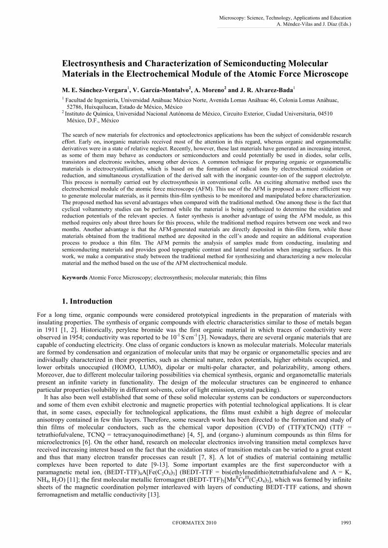
The following acceptor compounds were studied: (1) 1-trifluoromethanesulfonyl-6-phenylamine-1-azahexa-1,3,5-
triene, (2) 1-trifluoromethanesulfonyl-3-chloro-6-phenylamine-1-azahexa-1,3,5-triene, (3) 1-trifluoromethanesulfonyl-
3-[4’-(1’-trifluoromethanesulfonyl)-1’,4’-dihydropyridinyl]-6-allylamine)-1-azahexa-1,3,5-triene and (4) 1-
trifluoromethanesulfonyl–3-[2’(-(S)-(1’’-methyl) pyrrolidine)]-6-methylphenylamine-1-azahexa-1,3,5-triene (Figure 1).
The counter-ion used was potassium (III) trioxochromate, K3[Cr(C2O4)3]·3H2O.
N N SO2CF3
H X
SY N
R''
R
CF3O2
R'
1 X = H 2 X = Cl3 Y = CH, R = C5H4NSO2CF3, R' = H, R'' = CH2CHCH24 Y = N, R = C4H6NCH3, R' = CH3, R'' = Ph
Fig. 1. Chemical structure of pentamethine compounds
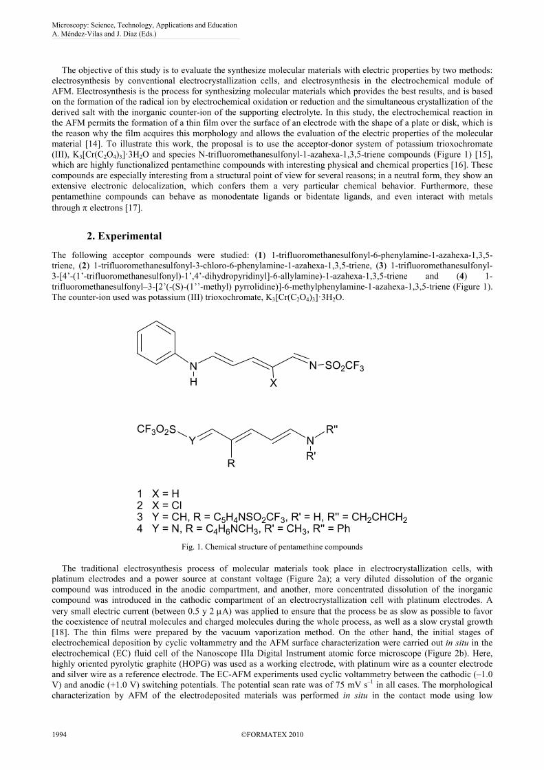
The traditional electrosynthesis process of molecular materials took place in electrocrystallization cells, with
platinum electrodes and a power source at constant voltage (Figure 2a); a very diluted dissolution of the organic
compound was introduced in the anodic compartment, and another, more concentrated dissolution of the inorganic
compound was introduced in the cathodic compartment of an electrocrystallization cell with platinum electrodes. A
very small electric current (between 0.5 y 2 µA) was applied to ensure that the process be as slow as possible to favor
the coexistence of neutral molecules and charged molecules during the whole process, as well as a slow crystal growth
[18]. The thin films were prepared by the vacuum vaporization method. On the other hand, the initial stages of
electrochemical deposition by cyclic voltammetry and the AFM surface characterization were carried out in situ in the
electrochemical (EC) fluid cell of the Nanoscope IIIa Digital Instrument atomic force microscope (Figure 2b). Here,
highly oriented pyrolytic graphite (HOPG) was used as a working electrode, with platinum wire as a counter electrode
and silver wire as a reference electrode. The EC-AFM experiments used cyclic voltammetry between the cathodic (–1.0
V) and anodic (+1.0 V) switching potentials. The potential scan rate was of 75 mV s–1
in all cases. The morphological
characterization by AFM of the electrodeposited materials was performed in situ in the contact mode using low
Microscopy: Science, Technology, Applications and Education A. Méndez-Vilas and J. Díaz (Eds.)
1994 ©FORMATEX 2010
______________________________________________
scanning forces (0.3 N.m
–2) at the open circuit mode. For this study, 0.1 M tetrabutylammonium tetrafluoroborate was
used as support electrolyte. The AFM characterization of the electrodeposited material was performed in the presence of
the aqueous electrolyte (50 µl). In order to compare the electrode surface modifications before and after deposition, the
HOPG was imaged before the electrochemical reactions and after different potential scan cycles (PSC).
Elemental analysis of the electrodeposited films was performed with a scanning electron microscope (SEM) Jeol
JSM5900 coupled to an energy-dispersive spectrophotometer (EDS) working at 20 keV. The acquisition of the EDS
data was stopped when it reached 5000 counts. The infrared spectra were obtained with an IR spectrophotometer Perkin
Elmer 282-B. The spectra were recorded by the KBr-pellet technique. Finally, the electric conductivity of the films was
studied by means of a four-point probe. For these measurements, the molecular films onto the HOPG substrates were
analyzed with four metallic strips that acted as electrodes for the electrical measurements. In order to get an ohmic
behavior between the deposited films and the metallic electrodes, four gold or silver strips were deposited by vacuum
thermal evaporation onto the glass slices. To prevent the strips from reaching the surface of the substrate, a
molybdenum boat with two grids was used as the evaporation source. The boat temperature was 473 °C during
evaporation, as measured with a chromel-alumel thermocouple. The electric current as a function of temperature was
measured with an applied voltage of 100 V in the ohmic regime by using a programmable voltage source Keithley 230
and a peak-ammeter Keithley 485 coupled to an HP3421 data collector.
(a)
(b)
Fig. 2. Electrosynthesis cell for (a) conventional electrosynthesis and (b) AFM electrosynthesis
The proposed method consisted of arranging the electrochemical module of the AFM as an electrosynthesis cell,
composed of a conducting, highly oriented pyrolytic graphite (HOPG) substrate, permitting the observation of changes
at the surface of the substrate. The graphite is mounted over a metallic disc by conducting glues that assure conductivity
between graphite and disc. At the center of the graphite substrate, a teflon sheave (washer) was placed containing the
electrolytic solution constituted by the donor and acceptor species (figure 2b). This electrochemical cell, unlike
conventional electrochemical cells (figure 2a), consists of three electrodes: the reference electrode and the counter-
electrode, consisting of thin wires, and the working, or task, electrode, where the deposition of synthesized material
occurs and which has a flat surface area larger than those of the other two electrodes. The AFM works by scanning a
high resolution tip over the surface under study -which in this case refers to the surface of the material formed in situ.
In this way, one can observe the growth of material as it settles on the surface layer. The pyramid-shaped tip is placed at
the end of a hoop or strip of a hundred microns length. The tip deflects as it closely traces the surface of the contour
Platinum electrode
Anodic compartment
Current source
Cathodiccompartment
Porous plate
Platinum electrode
Anodic compartment
Current source
Cathodiccompartment
Porous plate
Microscopy: Science, Technology, Applications and Education A. Méndez-Vilas and J. Díaz (Eds.)
©FORMATEX 2010 1995
______________________________________________
underneath, and the magnitude of the deflection is detected by an optic system coupled to an electronic mechanism that
provides the topographic information from the sample. The use of AFM for the synthesis of molecular materials permits
the study of the reduction-oxidation electrochemical processes occurring in the cell, with the aid of an electrochemical
module (potentiostat/galvanostat). The electrochemical modification of molecular materials as they synthesize and settle
over the task (graphite) electrode can thus be studied in real time.
3. Results and discussion
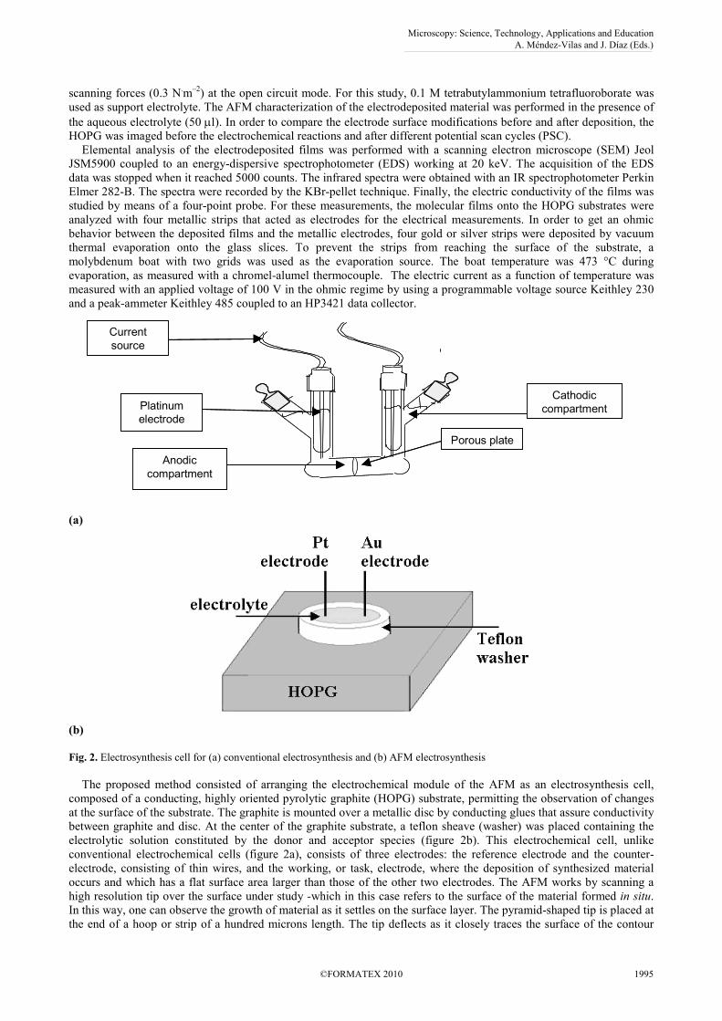
It is normally required to investigate the redox behavior of the starting compounds and to discard an independent
reaction of the solutions [19], a cyclic-voltammetry study on each of them was performed. Figure 3 shows the cyclic
voltammetry response of donor species 3 alone. The first positive scan shows an oxidation peak at +420 mV and a very
small reduction peak at +50 mV Vs Ag. After the first cycle, the voltammetric profile was considerably different, with
an important reduction in current density. The first advantage of using the AMF electro-synthesis module is found at
this point, as the redox study initially required in the molecular materials’ electro-synthesis can be performed in the
AFM as soon as the material is formed, while the conventional method requires two isolated steps (the redox study
followed by the electro-synthesis step.
Fig. 3. Cyclic voltammogram for the ethanol-water dissolution containing (a) only compound 3 after 5 PSC and (b) compound 3 and
K3[Cr(C2O4)3]·3H20 species (combined) after 10 PSC. The potential sweep rate was 75 mV s-1.
The electro-synthesis was carried out repeatedly, modifying operation parameters such as working temperature,
reagents’ concentration, electric current intensity, solvent used and type of electrodes. It is noteworthy that the time to
perform an electro-synthesis can go from one or two weeks to almost two months, considerably more than the
corresponding AFM crystallization and synthesis processes. Figure 4 shows AFM images of the electrode surface after
a) 0 (bare HOPG surface) and b) 30 potential scan cycles (PSC) when using DS1 and the [Cr(C2O4)3]3-
anion. The
electrodeposited material in this case is almost uniformly distributed on the electrode surface and the final film texture
is thin and grainy. From the vertical scale bar, it is clear that the size of the grains is very small. A root mean square
(RMS) roughness analysis of the surface, which is a quantitative measurement of the film texture, shows that the film
Microscopy: Science, Technology, Applications and Education A. Méndez-Vilas and J. Díaz (Eds.)
1996 ©FORMATEX 2010
______________________________________________
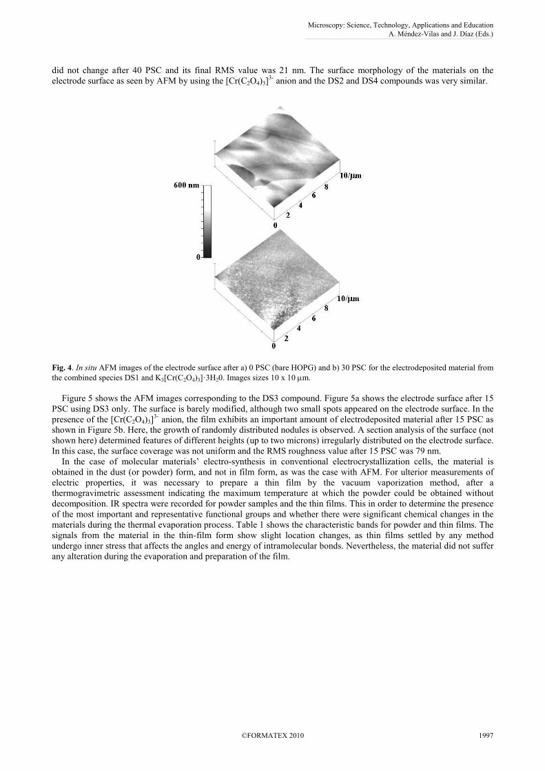
did not change after 40 PSC and its final RMS value was 21 nm. The surface morphology of the materials on the
electrode surface as seen by AFM by using the [Cr(C2O4)3]3-
anion and the DS2 and DS4 compounds was very similar.
Fig. 4. In situ AFM images of the electrode surface after a) 0 PSC (bare HOPG) and b) 30 PSC for the electrodeposited material from
the combined species DS1 and K3[Cr(C2O4)3]·3H20. Images sizes 10 x 10 µm.
Figure 5 shows the AFM images corresponding to the DS3 compound. Figure 5a shows the electrode surface after 15
PSC using DS3 only. The surface is barely modified, although two small spots appeared on the electrode surface. In the
presence of the [Cr(C2O4)3]3-
anion, the film exhibits an important amount of electrodeposited material after 15 PSC as
shown in Figure 5b. Here, the growth of randomly distributed nodules is observed. A section analysis of the surface (not
shown here) determined features of different heights (up to two microns) irregularly distributed on the electrode surface.
In this case, the surface coverage was not uniform and the RMS roughness value after 15 PSC was 79 nm.
In the case of molecular materials’ electro-synthesis in conventional electrocrystallization cells, the material is
obtained in the dust (or powder) form, and not in film form, as was the case with AFM. For ulterior measurements of
electric properties, it was necessary to prepare a thin film by the vacuum vaporization method, after a
thermogravimetric assessment indicating the maximum temperature at which the powder could be obtained without
decomposition. IR spectra were recorded for powder samples and the thin films. This in order to determine the presence
of the most important and representative functional groups and whether there were significant chemical changes in the
materials during the thermal evaporation process. Table 1 shows the characteristic bands for powder and thin films. The
signals from the material in the thin-film form show slight location changes, as thin films settled by any method
undergo inner stress that affects the angles and energy of intramolecular bonds. Nevertheless, the material did not suffer
any alteration during the evaporation and preparation of the film.
Microscopy: Science, Technology, Applications and Education A. Méndez-Vilas and J. Díaz (Eds.)
©FORMATEX 2010 1997
______________________________________________
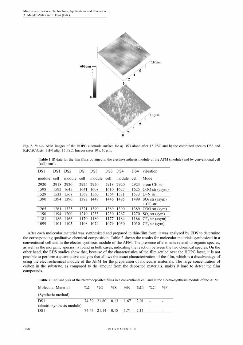
Fig. 5. In situ AFM images of the HOPG electrode surface for a) DS3 alone after 15 PSC and b) the combined species DS3 and
K3[Cr(C2O4)3]·3H20 after 15 PSC. Images sizes 10 x 10 µm.
Table 1 IR data for the thin films obtained in the electro-synthesis module of the AFM (module) and by conventional cell
(cell), cm-1.
DS1
module
DS1
cell
DS2
module
DS
cell
DS3
module
DS3
cell
DS4
module
DS4
cell
vibration
Mode
2920 2918 2920 2925 2920 2918 2920 2923 arom CH str
1598 1592 1645 1641 1608 1610 1627 1625 COO str (asym)
1529 1533 1568 1569 1560 1564 1531 1533 C=N str
1390 1394 1390 1388 1449 1446 1495 1499 SO2 str (asym)
+ CC str.
1265 1261 1325 1321 1390 1389 1390 1389 COO str (sym)
1190 1194 1200 1210 1233 1230 1267 1270 SO2 str (sym)
1181 1186 1166 1170 1180 1177 1184 1186 CF3 str (asym)
1099 1101 1105 1108 1074 1079 1030 1030 CF3 str (sym)
After each molecular material was synthesized and prepared in thin-film form, it was analyzed by EDS to determine
the corresponding qualitative chemical composition. Table 2 shows the results for molecular materials synthesized in a
conventional cell and in the electro-synthesis module of the AFM. The presence of elements related to organic species,
as well as the inorganic species, is found in both cases, indicating the reaction between the two chemical species. On the
other hand, the EDS studies show that, because of the characteristics of the film settled over the HOPG layer, it is not
possible to perform a quantitative analysis that allows the exact characterization of the film, which is a disadvantage of
using the electrochemical module of the AFM for the preparation of molecular materials. The large concentration of
carbon in the substrate, as compared to the amount from the deposited materials, makes it hard to detect the film
compounds.
Table 2 EDS analysis of the electrodeposited films in a conventional cell and in the electro-synthesis module of the AFM
Molecular Material
(Synthetic method)
%C %O %S %K %Cr %Cl %F
DS1
(electro-synthesis module)
74.39 21.80 0.13 1.67 2.01 - -
DS1 74.43 21.14 0.18 1.71 2.11 - -
Microscopy: Science, Technology, Applications and Education A. Méndez-Vilas and J. Díaz (Eds.)
1998 ©FORMATEX 2010
______________________________________________
(conventional cell)
DS2
electro-synthesis module
77.88 18.70 0.15 1.76 0.71 0.10 0.70
DS2
(conventional cell)
77.08 18.29 0.20 1.92 0.78 0.13 0.76
DS3
(electro-synthesis module)
76.42 17.38 0.23 3.99 1.40 - 0.58
DS3
(conventional cell)
76.44 17.41 0.19 4.03 1.44 - 0.61
DS4
(electro-synthesis module)
42.05 38.92 0.97 9.29 6.18 - 2.59
DS4
(conventional cell)
42.15 38.89 0.91 9.32 6.27 - 2.70
The electrical conductivity of each material was evaluated at 25°C. The results are presented in Table 3, which shows
that the thin film synthesized in the AFM is the one with the largest conductivity, possibly due to graphite’s conducting
nature and to better ordering in the synthesized material. The conductivity values at room temperature for both materials
are in the range of electric conductivities for semiconducting molecular materials (102 to 10
-6 S/m) [20]. This is
important because a molecular semiconductor is generally defined in terms of its conductivity at room temperature,
besides its structure, stacking form and orbital overlap. The presence of adhesive conductors between the substrate and
the metallic discs that hold the sample to the microscope may be a disadvantage of the AFM electrosynthesis process, as
they may interfere with the measurement of conductivity in the transversal direction with respect to the electrode.
Table 3 Electrical conductivity results for electrodeposited films in a conventional cell and in the electro-synthesis module
of the AFM (T = 25°C).
Molecular Material
(Synthetic method)
Electrical
conductivity
σ (Scm-1
);
DS1 (electro-synthesis module) 4.5 x 10⁴
DS1 (conventional cell) 2.3 x 10⁻⁶
DS2 (electro-synthesis module) 5.7 x 10⁴
DS2 (conventional cell) 2.5 x 10⁻⁶
DS3 (electro-synthesis module) 6.3 x 10⁴
DS3 (conventional cell) 6.2 x 10⁻⁶
DS4 (electro-synthesis module) 6.9 x 10⁴
DS4 (conventional cell) 6.3 E10-6
4. Conclusions
Electrosynthesis produces molecular materials with amorphous appearance in electrochemical cells, as well as in the
electro-crystallization module of the AFM. The traditional method is extremely slow compared to the alternative
procedure using the AFM, which could be the most recommendable method for thin-film manufacturing. The traditional
method, which generates molecular material in the powder form, requires an additional step of vacuum vaporization for
thin-film production.
On the other hand, a greater amount of molecular material is produced in the electrochemical cells, due to the cell
size, which is larger than the one used in the AFM electro-synthesis module. Nevertheless, from the structural and
chemical standpoints, both techniques lead to molecular materials formed by the electrochemical oxidation of neutral
molecules that give rise to compounds of mixed valence. In both cases, in order to get a salt derived from an electronic
donor, a much diluted dissolution of donor is introduced in the anodic compartment, as the solution of the basic salt is in
the cathodic compartment. The role of the basic salts in both electrocrystallizations is twofold: first, to ensure the
conductivity by acting as the supporting electrolyte, and then to provide the counter-ion for the ionic radical salt to
form.
The method here proposed has considerable advantages when compared with the traditional method: in first place,
the fact that the synthesis of material can be carried out at the same time as the cyclic voltammetry study permits the
determination of the reduction and oxidation potentials of the involved species, while the traditional method requireds
two different stages (namely, cyclic voltammetry followed by the electro-synthesis of the material). A second advantage
is the faster synthesis of materials, which requires about three hours in the AFM, while the traditional method takes
from one week to two months. Furthermore, the materials settle in film form when using the AFM, whereas those
Microscopy: Science, Technology, Applications and Education A. Méndez-Vilas and J. Díaz (Eds.)
©FORMATEX 2010 1999
______________________________________________
obtained by the traditional method settle as powder in the anode of the cell and must be vaporized before a thin film is
available. Some objections can be set at the AFM method proposed in this work, concerning some techniques that may
provide a better characterization of the synthesized materials: using conventional electro-synthesis, the material is
produced in powder form that is suitable for analysis with techniques such as IR spectroscopy, elemental analysis, and
X-ray diffraction, among others. The films obtained at the electro-synthesis module of the microscope, can only be
analyzed by techniques such as EDS, which does not provide enough information about the structural and chemical
composition of the materials. Moreover, from the information provided by the EDS, the material that is going to be used
as task electrode must be very carefully chosen in order to clearly discern between the chemical elements belonging to
the electrodeposited material and those that belong to the conductor substrate. The amount of material that is deposited
on the working electrode surface is limited by the small volume of electrolyte (50µl) that is introduced in the
electrochemical cell. The measurement of electric properties of materials synthesized in the electrochemical module of
the microscope is affected by the conducting graphite substrate over which they are deposited, so it was not possible to
evaluate the dependence of electric current on temperature, which was possible when working with films of molecular
materials prepared by the conventional method.
Acknowledgements The support by CONACYT (Mexico), project number 102401, is gratefully acknowledged.
References
[1] Saito G, Yoshida Y, Development of Conductive Organic Molecular Assemblies: Organic Metals, Superconductors, and Exotic
Functional Materials. Bull. Chem. Soc. Jpn. 2007, 80, 1-137.
[2] Wudl F.From Organic Metals to Superconductors: Managing Conduction Electrons in Organic Solids. Acc. Chem. Res., 1984,
17, 227
[3] Akamatu H, Inokuchi H, Matsunaga Y, Electrical Conductivity of the Perylene-Bromine complex. Nature, 1954, 173, 168-170.
[4] Caro J, Garelik S and Figeras A, Anisotropic Materials Prepared by OCVD: Organic Molecular Conductors. Chem. Vap.
Deposition, 1996, 2, 251-253.
[5] Figueras A, Garelik S., Caro J, Cifré J, Veciana J, Rovira C, Ribera E, Canadell E., Seffar A, Fontcuberta J, Preparation and
characterization of conducting thin films of molecular organic conductors (TTF-TCNQ)J. Cryst. Growth, 1996, 166, 798-803
[6] Stringfellow G B Organometallics Chemical Vapor Epitaxy: Theory and Practice. 1st ed. New York, Academic Press,1989.
[7] Astruc D, From Organotransition-Metal Chemistry toward Molecular Electronics: Electronic Communication between Ligand-
Bridged Metals. Acc. Chem. Res. 1997, 30, 383-391.
[8] Toma H E, Molecular Materials and Devices: Developing New Functional Systems Based on the Coordination Chemistry
Approach. J. Braz. Chem. Soc., 2003, 14, 845-869.
[9] Graham A W, Kurmoo M, Day P, β’’-(bedt-ttf)4[(H2O)Fe(C2O4)3]·PhCN: the first molecular superconductor containing
paramagnetic metal ions. J. Chem. Soc., Chem. Commun. 1995, 2061-2062.
[10] A. Rodríguez, M.E. Sánchez Vergara, V. García Montalvo, A. Ortiz, J.R. Alvarez, Thin Films of Molecular Materials
Synthesized from C32H20N10M (M= Co, Pb, Fe): Film Formation, Electrical and Optical Properties, Appl. Surf. Sci. 2010, 256,
3374.
[11] Coronado E, Galán-Mascarós J R, Gómez-García C J, Laukhin V, Coexistence of ferromagnetism and metallic conductivity in a
molecule-based layered compound. Nature 2000, 408, 447-449.
[12] Kurmoo M, Graham A W, Day P, Coles S J, Hurtshouse M B, Caulfield J L, Singleton J, Pratt F L, Hayes W, Ducasse L,
Guionneau P, Superconducting and Semiconducting Magnetic Charge Transfer Salts: (BEDT-
TTF)4AFe(C2O4)3.cntdot.C6H5CN (A = H2O, K, NH4). J. Am. Chem. Soc. 1995, 117, 12209-12217.
[13] Coronado E, Galán-Mascarós J R, Giménez-Saiz C, Gómez-García C J, Ruiz-Pérez C, Hybrid Organic/Inorganic Molecular
Materials Formed by Tetrathiafulvalene Radicals and Magnetic Trimeric Clusters of Dimetallic Oxalate-Bridged Complexes:
The Series (TTF)4{MII(H2O)2[MIII(ox)3]2}·nH2O (MII = Mn, Fe, Co, Ni, Cu and Zn; MIII = Cr and Fe; ox = C2O42-). Eur. J.
Inorg. Chem. 2003, 2290-2298.
[14] Sánchez Vergara ME, Ruíz Farfán M A, Ortiz A, Rivera M, Alvarez-Toledano C, Síntesis y caracterización de materiales
moleculares de ftalocianinas metálicas en el m´odulo electroquímico del microscopio de fuerza atómica. Rev. Mex. Fís. 2005,
51,535-541.
[15] Rivera M, Alvarez Toledano C, Moreno A, Sepúlveda Sánchez J D, Hernández Pérez T, Sánchez Vergara M E, Electrochemical
and Atomic Force Microscopy investigations of new materials from N-Trifluoromethanesulfonyl-1-azahexa-1,3,5-trienes
derivatives. J. Braz. Chem.Soc., 2005, 16, 3A, 316-321.
[16] Toscano R A, Rosas R, Hernández-Galindo M C, Alvarez-Toledano C, García-Mellado O, Synthesis and structural
characterization of tricarbonyl 1-azahexa-1,3,5-triene iron(0) complexes. Transit. Metal. Chem., 1998, 23, 113-116.
[17] Toscano R A, Hernández-Galindo M C, Rosas R, Garcia-Mellado O, Portilla FD, Amabile-Cuevas C, Alvarez-Toledano C,
Nucleophilic Reactions on 1-Trifluoromethanesulfonylpyridinium Trifluoromethanesulfonate (Triflypyridinium Triflate,
TPT).Ring-Opening and "Unexpected" 1, 4-Dihydropyridine Reaction Products. Chem. Pharm. Bull. 1997, 45, 957-961.
[18] Rivera M, Alvarez-Toledano C, Moreno A, Sepúlveda-Sánchez J D, Hernández-Pérez T, Sánchez-Vergara ME,
Electrochemical and Atomic Force Microscopy Investigations of New Materials from N-Trifluoromethanesulfonyl-1-azahexa-
1,3,5-trienes Derivatives. J. Braz. Chem. Soc. 2005, 16, 316-321.
[19] Saito G, Ferraris J P, requirements for an “organic metal”. Bull. Chem. Soc. Jpn. 1980, 26 2141-2145.
[20] Kiani M S; Mitchell G R, Structure property relationships in electrically conducting copolymers formed from pyrrole and N-methyl pyrrole.
Synth. Met. 1992, 46, 293
Microscopy: Science, Technology, Applications and Education A. Méndez-Vilas and J. Díaz (Eds.)
2000 ©FORMATEX 2010
______________________________________________