electronics- quartus-ii-creating-your-first-sopc-with
TRANSCRIPT

https://www.badprog.com/electronics-
quartus-ii-creating-your-first-sopc-with-
qsys-and-nios-ii-software
Electronics - Quartus II - Creating your
first SoPC with Qsys and Nios II software
Submitted by Mi-K on Sunday, April 6, 2014 - 4:47pm
Qsys is the new Altera SOPC Builder tool. So if you are using Quartus 13.0.x, you should
have it.
Then, don't be surprised not having, for example, the simple SOPC Builder tool in your
Quartus version.
It's just normal because Qsys is the new name of the SOPC Builder and its improvement.
That said, let's get started with this tutorial and let's create your first System on
Programmable Chip (SoPC) or System on Chip (SoC) with Qsys.
Explanation
For this tutorial, we will realize a system which lights two LEDs from two switchers.
We will use the Altera DE1 board and Quartus II 13.0sp1.
If you had the DE2, you would have only few things to change. So keep reading.
It’s not so easy to all understand first time, but at the end you will be proud to achieve this
really interesting tutorial.
This project is a mix between hardware and software.
We’re indeed going to choose which parts of hardware we want, realize the design and then
create a software library from this design. Then we will be able to create a program in C
language in order to upload this program into the DE1 board.
For that, the design hardware will be created with Qsys and a file will be generated, that’s
de1_blinker.sopcinfo.

With this file we will be able to create the BSP (Board Support Package) that it will be
compiled with our user application in C language.
The user application and the BSP will be created with SBT (Software Build Tools).
These tools are composed of:
GCC A special Nios II GNU library C
A HAL (Hardware Abstraction Layer)
SBT is a tool based on Eclipse, a well known open source IDE.
You don’t need to have Eclipse already installed because the Indigo version will be launched
for you when you will decide to create your BSP.
Indeed a hidden Eclipse was installed with your Quartus installation.
After the compilation and the linkage of the user application and the BSP, a new file will be
added: de1_blinker.elf.
At this point, we will send it to the board in order to program it.
Finally we will see the result directly on the board with red LEDs lit from switchers.
Creating a project from Quartus
We have first of all to create a new Quartus project.
From Quartus > File > New Project Wizard…
Project name: chip1
Project directory: C:\dev\fpga\altera\sys-on-prog-chip
Project top-level entity: chip1
Next > Next >
Family: Cyclone II
Package: FBGA
Pin count: 484
Speed grade: 7
Available devices: EP2C20F484C7
Next > Next > Finish
Creating an interaction between components with Qsys
From Quartus > Tools > Qsys

Qsys opens.
Click File > Save > the Save windows should open direct from the sys-on-prog-chip directory
> then enter the name de1_blinker in the input text > Save.
In your project directory you can now see a new file: de1_blinker.qsys.
Let’s back to Qsys.
On the right you could see the clk_0 clock in the System Contents tab.
Let’s rename it by clock_main.
You can check all tabs to see what they contain. Everything is by default correct, so don’t
modify anything.
Let’s now add a new component.
Adding a processor
From Component Library (on the left), select: Library > Embedded Processors > Nios II
Processor.
Double-click it or click the +Add… button in order to add on the System Contents.
The Nios II Processor’s module window opens.
On the Core Nios II tab > Select a Nios II Core > Nios II/e > Finish
The Nios II core is added on the System Contents with the name nios2_qsys_0, let’s rename it
by nios2_proc.
You can see that the data_master and instruction_master are already linked to
jtag_debug_module with a black line passing by a tiny black round.
At the bottom, in the Messages tab, there are 4 errors.
Don’t be afraid, we will fix it in a few moment.
Adding a memory
Let’s continue by adding a new module: a memory.
Click Library > Memories and Memory Controllers > On-Chip > On-Chip Memory
(RAM or ROM) > +Add…
The On-Chip Memory (RAM or ROM)’s module window appears and in the Size area >
Total memory size you could see 4096 bytes.
This size is a bit short for our first example, so let’s replace it by 16384.
Click Finish.
The onchip_memory2_0 is added to the System Contents.
Rename it by onchip_memory.
There are now 6 errors at the bottom and 1 warning.
Adding a first PIO (for switchers)
Let’s continue by adding the PIO (Parallel I/O) module inputs:
Click Library > Peripherals > Microcontroller Peripherals > PIO (Parallel I/O) > +
Add…
The PIO (Parallel I/O)’s module window appears.
In the Basic Settings > Width (1-32 bits) > there is already 8 written. Even if we need only 2
switchers, let it like that. It will allows us to show how to assign location to the pins, later.
Still from the Basic Settings tab > Direction > select Input > Finish.
The PIO (Parallel I/O) module input has just been added to the System Contents.
Rename it from pio_0 to switcher.
Now there are 8 errors and 2 warnings.
Adding a second PIO (for LEDs)
Let’s continue by adding the second PIO (Parallel I/O) module outputs:
Click Library > Peripherals > Microcontroller Peripherals > PIO (Parallel I/O) > +
Add…
The PIO (Parallel I/O)’s module window appears.
In the Basic Settings tab > Width (1-32 bits) > there is already 8 written. This time change it
by 2.
Still from Basic Settings tab > Direction > select Output > Finish.
The PIO (Parallel I/O) module output has just been added to the System Contents.
Rename it from pio_0 to led.
Now there are 10 errors and 3 warnings.
Adding a system ID peripheral

It’s time to add the final module: the System ID Peripheral.
This module acts as a manager between hardware and the BSP.
Click Library > Peripherals > Debug and Performance > System ID Peripheral > +
Add…
The System ID Peripheral’s module window appears.
In Parameters > 32 bit System ID > change 0x00000000 by 1337 (it will be automatically
transformed into 0x00001337).
This number is arbitrary and must be unique.
Click Finish.
The System ID Peripheral’s module has just been added to the System Contents.
Rename it from sysid_qsys_0 to sysid_1337.
There are now 12 errors and 6 warnings.
Correcting errors, part 1
Let’s correct these errors and warnings.
First of all, let’s connect all the clocks together.
For that it’s necessary to click rounds in front of each clock, that’s:
nios2_proc > clk
onchip_memory > clk1
switcher > clk
led > clk
sysid_1337 > clk
Errors are reduced to 7 and warnings are still 6.
The clock_main.clk_reset output must also be assigned to other modules reset_n inputs.
For that, let’s connect them all.
Let’s connect clock_main.clk_reset to
nios2_proc > reset_n
onchip_memory > reset1
switcher > reset
led > reset
sysid_1337 > reset

Errors are decreased to 2 and warnings are still 6.
Correcting errors, part 2
Let’s now connect Avalon Memories together.
Let’s click the following rounds in order to connect nios2_proc.data_master to:
nios2_proc > jtag_debug_module
onchip_memory > s1
switcher > s1
led > s1
sysid_1337 > control_slave
Then click the following rounds in order to connect nios2_proc.instruction_master to:
nios2_proc > jtag_debug_module
onchip_memory > s1
There are now 10 errors and 2 warnings.
Let’s assign base addresses.
From Qsys > System > Assign Base Addresses
Errors: 2.
Warnings: 2.
Let’s reopen the nios2_proc module window by double-clicking it.
In Reset Vector > Reset vector memory > select onchip_memory.s1.
In Exception Vector > Exception vector memory > select onchip_memory.s1.
Click Finish.
Then we must connect the clock_main.clk_in_reset to:
nios2_proc > reset_n
Correcting errors, part 3
To finish the system, we have to add connections to external connections.
As you can see the switcher.external_connection is in a not defined state.
To solve it let’s double-click in the Export column for the switcher > external_connection
(Conduit).
The new Export becomes switcher_external_connection.

Do the same for the led > external_connection in the Export column.
The new Export becomes led_external_connection.
Errors: 0.
Warnings: 0.
We are done for the clicking black rounds part.
Generating HDL code
Let’s generate the Verilog HDL code.
From Qsys > select the Generation tab on the right, then click Generate at the bottom.
The Generate window appears with plenty of generating lines.
At the end of the generation, if you check your sys-on-prog-chip directory, you should see a
new de1_blinker folder and 5 new files in addition to de1_blinker.sys:
de1_blinker.bsf
de1_blinker.cmp
de1_blinker.html
de1_blinker.sopcinfo
de1_blinker.generation.rpt
Inside the de1_blinker folder there is another folder called synthetis.
Inside the synthetis folder another called submodules with a lot of files.
Let’s back to Quartus.
Adding files, compilation and upload from Quartus
Adding files
From Quartus > Project > Add/Remove Files in Project… > the Settings window appears.
Click the ”…” button at the right of the File name text input.
Select the file that you can find there:
C:\dev\fpga\altera\sys-on-prog-chip\de1_blinker\synthesis\de1_blinker.v
Then click Add on the right.
The de1_blinker.v file is added.
Let’s continue by adding all other files.

Click the ”…” button at the right of the File name text input.
Select all 36 files in the following directory:
C:\dev\fpga\altera\sys-on-prog-chip\de1_blinker\synthesis\submodules
They are all added immediately (don’t need here to click Add).
Click OK.
In the Project Navigator click the Files tab.
In the list of files, select de1_blinker/synthesis/de1_blinker.v.
Right click > Set as Top-Level Entity.
Compilations
Let’s start a first compilation.
From Quartus > Processing > Start Compilation.
Normally the compilation ends with no errors (only warnings).
This first compilation was to tell Quartus which pins we would like to use.
Let’s now assign correct pins with correct location.
From Quartus > Assignments > Pin Planner.
At the bottom, in the All Pins area, you should see Node Name but without their Location
nor their I/O Bank and VREF Group.
To resolve this, we have to open the DE1_pin_assignments.csv, normally provided by
Altera.
Notice that this assignments is only for the DE1 board. For the another board use the specific
pin assignments CSV file.
Inside we can see that the CLOCK_50’s location is PIN_L1.
We have to add each location to each node.
So, in the Pin Planner, double-click the Location of clk_clk > select PIN_L1.
Automatically the I/O Bank and the VREF Group are added.
Notice: SW2 to SW7 are not used for this tutorial, so you don't have to assign them if you
don't want to.
Let’s do the same for other nodes:
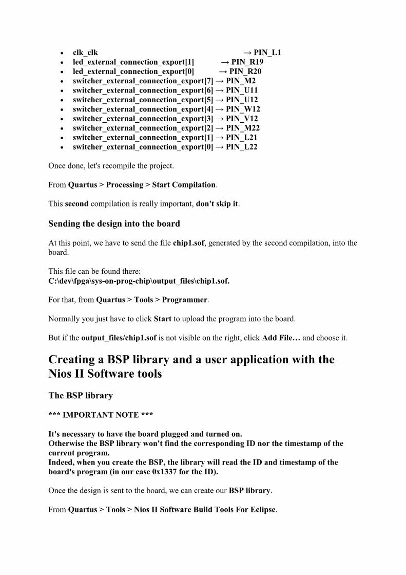
clk_clk → PIN_L1
led_external_connection_export[1] → PIN_R19
led_external_connection_export[0] → PIN_R20
switcher_external_connection_export[7] → PIN_M2
switcher_external_connection_export[6] → PIN_U11
switcher_external_connection_export[5] → PIN_U12
switcher_external_connection_export[4] → PIN_W12
switcher_external_connection_export[3] → PIN_V12
switcher_external_connection_export[2] → PIN_M22
switcher_external_connection_export[1] → PIN_L21
switcher_external_connection_export[0] → PIN_L22
Once done, let's recompile the project.
From Quartus > Processing > Start Compilation.
This second compilation is really important, don't skip it.
Sending the design into the board
At this point, we have to send the file chip1.sof, generated by the second compilation, into the
board.
This file can be found there:
C:\dev\fpga\sys-on-prog-chip\output_files\chip1.sof.
For that, from Quartus > Tools > Programmer.
Normally you just have to click Start to upload the program into the board.
But if the output_files/chip1.sof is not visible on the right, click Add File… and choose it.
Creating a BSP library and a user application with the
Nios II Software tools
The BSP library
*** IMPORTANT NOTE ***
It's necessary to have the board plugged and turned on.
Otherwise the BSP library won't find the corresponding ID nor the timestamp of the
current program.
Indeed, when you create the BSP, the library will read the ID and timestamp of the
board's program (in our case 0x1337 for the ID).
Once the design is sent to the board, we can create our BSP library.
From Quartus > Tools > Nios II Software Build Tools For Eclipse.

Eclipse Indigo launches then choose a workspace, for example:
C:\dev\fpga\eclipse
From Eclipse > File > New > Nios II Application and BSP from Template.
The Nios II Application and BSP from Template window appears.
In SOPC Information File name go to choose:
C:\dev\fpga\sys-on-prog-chip\de1_blinker.sopcinfo
Automatically in the CPU name part you can see nios2_proc appears in the drop-down
menu.
Add a name in the Project name part, for example blinker-lib.
In the Project template, let Hello World as template.
Click Next, you should see blinker-lib_bsp as BSP Project name.
Click Finish.
The compilation of the BSP library starts and you can find two new projects there:
C:\dev\fpga\sys-on-prog-chip\software
In the Project Explorer, there is then two new projects:
blinker-lib
blinker-lib_bsp
Let’s remove blinker-lib or just close it because we don’t need it at all.
A user application
It’s time now to create a user application.
From Eclipse > File > New > Nios II Application.
Let’s add a name in the Project name, for example app-to-board.
Then in the BSP location, choose blinker-lib_bsp.
Click Finish.
Let’s now create a C file.
From the Project Explorer > right-click app-to-board > New > Source File.
As Source file, type main.c.
As Template, choose Default C source template.
Click Finish.
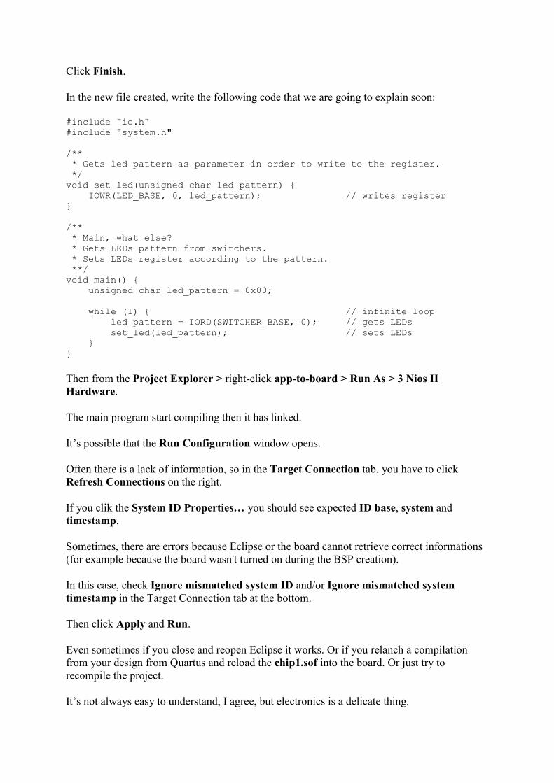
In the new file created, write the following code that we are going to explain soon:
#include "io.h"
#include "system.h"
/**
* Gets led_pattern as parameter in order to write to the register.
*/
void set_led(unsigned char led_pattern) {
IOWR(LED_BASE, 0, led_pattern); // writes register
}
/**
* Main, what else?
* Gets LEDs pattern from switchers.
* Sets LEDs register according to the pattern.
**/
void main() {
unsigned char led_pattern = 0x00;
while (1) { // infinite loop
led_pattern = IORD(SWITCHER_BASE, 0); // gets LEDs
set_led(led_pattern); // sets LEDs
}
}
Then from the Project Explorer > right-click app-to-board > Run As > 3 Nios II
Hardware.
The main program start compiling then it has linked.
It’s possible that the Run Configuration window opens.
Often there is a lack of information, so in the Target Connection tab, you have to click
Refresh Connections on the right.
If you clik the System ID Properties… you should see expected ID base, system and
timestamp.
Sometimes, there are errors because Eclipse or the board cannot retrieve correct informations
(for example because the board wasn't turned on during the BSP creation).
In this case, check Ignore mismatched system ID and/or Ignore mismatched system
timestamp in the Target Connection tab at the bottom.
Then click Apply and Run.
Even sometimes if you close and reopen Eclipse it works. Or if you relanch a compilation
from your design from Quartus and reload the chip1.sof into the board. Or just try to
recompile the project.
It’s not always easy to understand, I agree, but electronics is a delicate thing.

At the end of the process, you should see in the console, something like that:
Using cable "USB-Blaster [USB-0]", device 1, instance 0x00
Pausing target processor: not responding.
Resetting and trying again: OK
Reading System ID at address 0x00009020: verified
Initializing CPU cache (if present)
OK
Downloading 00004000 ( 0%)
Downloading 00004F0C (61%)
Downloaded 4KB in 0.0s
Verifying 00004000 ( 0%)
Verifying 00004F0C (61%)
Verified OK
Starting processor at address 0x00004020
If yes, then the program is into the board.
Try to push switchers SW0 and SW1 to high, you should see LEDR0 and LEDR1 light
respectively.
Explaining the code
IORD() is a define that can be found in the io.h file.
The first argument is the base, that we already created with Qsys.
Indeed the SWITCHER_BASE is a define that can be found in the system.h file.
With this base, we know which switcher is low or high.
IOWR() is also a define that can be found in the io.h file.
We specify the LED_BASE as first parameter, it can be found in the system.h file as well.
The second parameter is the offset register number (let it at 0).
The third parameter is the LEDs that we want to light.
So if we type:
IOWR(LED_BASE, 0, 0) → no one will be lit
IOWR(LED_BASE, 0, 1) → one will be lit (the LEDR0)
IOWR(LED_BASE, 0, 2) → one will be lit (the LEDR1)
IOWR(LED_BASE, 0, 3) → both will be lit (the LEDR0 and LEDR1)
Why?
Because in binary:
0 = 0000
1 = 0001
2 = 0010
3 = 0011
Each time there is a 1, a LED is lit.
Hence with 11, both LEDs are lit.
And according to our switchers, if:
SW0 is high, led_pattern is equal to 1 in decimal and 0000 0001 in binary.
SW1 is high, led_pattern is equal to 2 in decimal and 0000 0010 in binary.
SW0 and SW1 are high, led_pattern is equal to 3 in decimal and 0000 0011 in binary.
Conclusion
A huge step has been made.
You have successfully realized a system on programmable chip.
That means you successively used Qsys to realize interaction of hardware components and
generate the HDL design, used Quartus to compile the .SOF file in order to upload it into the
board with the Programmer tool.
After that you have generated a BSP library to combine with a user application so that create
an .ELF file and upload it into the board.
All that to light and turn off two LEDs with two switchers.
It can be a long way to achieve a tiny result, but it’s instead a giant step in your FPGA
comprehension.
Great job, you’ve made it.
‹ Electronics - Quartus II up Electronics - Quartus II - Installing ModelSim-Altera Starter
Edition ›
Comments
Dandy_Don (not verified)
Friday, December 5, 2014 - 12:11am
Permalink
AWESOME tutorial!! I have
Comment:
AWESOME tutorial!! I have been looking for something like this for a long time! You're
step-by-step instructions are just what I need!
THANKS!
reply
DJLinux (not verified)
Tuesday, June 2, 2015 - 5:08am
Permalink
Fantastic step by step
Comment:
Fantastic step by step tutorial thank you so much.
I got my first cheap FPGA chip a week ago.
Readed tons of PDFs data sheets, verilog versus VHDL and so.
I got my first blinking led very quickly but the NIOS II part was unclear.
But it's history now :-)
DJ
reply
andre_teprom (not verified)
Sunday, October 18, 2015 - 4:29pm
Permalink
Added to my favorites.
Comment:
Added to my favorites.
Just a question: Did you used the QuartusII subscribed version, or the Web version ?
Thanks
reply
Mi-K
Sunday, October 18, 2015 - 9:16pm
Permalink
Hello andre,
Comment:
Hello andre,

I used the Quartus II Web Edition.
reply
phd student (not verified)
Sunday, November 8, 2015 - 12:12am
Permalink
it doesn't work , elf file
Comment:
it doesn't work , elf file can not be created, pleeeease help
reply
corollary (not verified)
Saturday, February 27, 2016 - 10:05pm
Permalink
I had the same error, and
Comment:
I had the same error, and this fix worked for me:
Right-click on main.c in your app-to-board project, and select "Add to NIOSII build"
Then rebuild your bsp project, then try and run your app-to-board project again.
reply
hazemtn (not verified)
Thursday, March 3, 2016 - 3:54pm
Permalink
Downloading 00004000 ( 0%)
Comment:
Downloading 00004000 ( 0%)
Downloading 00004F0C (61%)
Downloaded 4KB in 0.0s

Verifying 00004000 ( 0%)
Verifying 00004F0C (61%)
Verified OK
Starting processor at address 0x00004020
dont but the when i click on switchers nothing happen !!!
reply
aleko (not verified)
Wednesday, March 23, 2016 - 10:04pm
Permalink
It does not work!!!! Project
Comment:
It does not work!!!! Project does not have an ELF file!!!!! I tried to do what corollary said and
my project was already added to NIOSII build. I have heard that this problem has to do with
the version of quartus, I am using quartus II version 13.0 web edition. I will appreciate some
help please.
Thanks in advance
reply
hesham1967 (not verified)
Sunday, April 15, 2018 - 4:08pm
Permalink
you must reconnect the
Comment:
you must reconnect the programmer
reply
Jaraqui (not verified)
Tuesday, September 6, 2016 - 11:31pm
Permalink
Unbelievable! This is
Comment:

Unbelievable! This is absolutely the most spetacular Nios tutorial I ever tried.
Here are some reasons:
1) It begins from scratch, i.e., no pre-filled files are used. Evertything has to be created;
2) The patience to write every step based on each event that is occurring produces me an
incredible feeling of safety to execute each one of them;
3) I executed this tutorial in an old EP2S60F672C5ES Nios Stratix II Development Kit
2004'board and, besides the .csv pin re-assignments, it was only necessary to assign the
PIN_J20 to receive a '1' constant level (which I did because the switcher inputs were leaved in
the default number, 8, but only two of them were used).
Thank you very much. I was stucked because my development board didn´t run new pre-filled
examples.
Excellent contribution.
reply
Mi-K
Wednesday, September 7, 2016 - 9:30pm
Permalink
:)
Comment:
Thank you for this comment Jaraqui.
reply
NightMare (not verified)
Friday, October 7, 2016 - 3:01pm
Permalink
thanks for sharing this...
Comment:
thanks for sharing this....its help me a lot
reply
Legend Lee (not verified)
Friday, November 11, 2016 - 7:35am
Permalink
Amazing NIOS II tutorial!
Comment:
Amazing NIOS II tutorial! Thanks al lot!!!
reply
Matt (not verified)
Monday, November 27, 2017 - 5:47am
Permalink
Not only do I have a "Project
Comment:
Not only do I have a "Project does not have an ELF file" but when I try to compile the main.c
as requested, I get an error that stops my compiling as "undefined reference to `main'" error
reply
Suryaa (not verified)
Monday, February 19, 2018 - 12:56pm
Permalink
Save the main.c file before
Comment:
Save the main.c file before building the project. Does away with the "project cannot find the
elf file" error.
reply
byambajav (not verified)
Friday, August 30, 2019 - 2:12pm
Permalink
Thanks, it helped me :)
Comment:

Thanks, it helped me :)
reply
Felipe Sarche (not verified)
Monday, July 2, 2018 - 4:54am
Permalink
Thanks, I was very usefull,
Comment:
Thanks, I was very usefull, can you explain me how to boot so it can run after power off
reply
David k. (not verified)
Saturday, September 22, 2018 - 3:35pm
Permalink
I did everything as
Comment:
I did everything as instructed but when i get to compilation i got errors : Error (12006): Node
instance "nios2_proc_instruction_master_translator" instantiates undefined entity
"de2_blinker_nios2_proc_instruction_master_translator"
no idea how to fix it....
reply
steve shepard (not verified)
Thursday, December 20, 2018 - 6:19am
Permalink
Hi, I'm really enjoying your
Comment:
Hi, I'm really enjoying your tutorial; just one little thing that I can't seem to get over; when I
compile I get the "top-level entity" not defined. I can't seem to find any module there (.v or
.vhd) that contains "ENTITY chip1 IS" to verify. Is possible to have access to some of your
source files so I can dig through? So much I'm trying to glean from your wisdom. Thanks!

reply
steve shepard (not verified)
Thursday, December 20, 2018 - 7:34am
Permalink
Solved! On my version of
Comment:
Solved! On my version of Quartus 13.1, the "best" way to set the proper module as top-level
entity:
Project ->set a top-level entity
No idea why my version is so different from yours, but it works! Thanks for slamming my
little brain forward!
reply
Hafiz (not verified)
Friday, December 6, 2019 - 1:49am
Permalink
Works perfectly....but canyou
Comment:
Works perfectly. But can you please tell me why we specifically used "1337" in system ID?
reply
Mi-K
Friday, December 6, 2019 - 2:51pm
Permalink
Hello Hafiz,
Comment:
Hello Hafiz,
"This number is arbitrary and must be unique."
