electronics quantities, ohm s law, series-parallel ... · electronics quantities, ohm’s law,...
TRANSCRIPT

2018/2019 – Semester 1 Page 2 1st edition – MJIIT (Sept. 2014) 2nd edition – KRS (Sept. 2015)
ELECTRONICS QUANTITIES, OHM’S LAW, SERIES-PARALLEL
RESISTIVE CIRCUITS AND POWER IN DC CIRCUIT
TOPICS:
1. ELECTRONIC QUANTITIES
2. OHM’S LAW
3. SERIES AND PARALLEL RESISTIVE CIRCUITS
4. POWER IN DC CIRCUIT
OBJECTIVES:
1. To measure voltage, current and resistance in a series DC circuit.
2. To demonstrate the relationship of resistance, current and voltage by using Ohm’s law
3. To obtain values for resistance, voltage and current in a series/parallel resistive circuit
by using Ohm’s law
4. To measure DC power in a resistive circuit
LIST OF INSTRUMENTS:
1. F.A.C.E.T Base Unit
2. DC Fundamental Circuit Board
3. OHM’S LAW circuit block
4. LINEAR/NONLINEAR VARIABLE RESISTOR circuit block
5. SERIES/PARALLEL CIRCUIT circuit block
6. POWER circuit block
7. Multimeter

2018/2019 – Semester 1 Page 3 1st edition – MJIIT (Sept. 2014) 2nd edition – KRS (Sept. 2015)
EXPERIMENT 1: ELECTRONIC QUANTITIES
Objective:
To measure voltage, current and resistance in a series DC circuit
Procedure:
1. Insert the DC FUNDAMENTALS circuit board into the base unit. Locate the OHM’S
LAW circuit block.
2. Record the color-coded bands for resistors R1 and R2. Determine the value and tolerance
of R1 and R2. Complete Table 1.1.
3. Measure and record the values of R1 and R2 using multimeter.
4. Insert a two-post connector between resistors R1 and R2.
5. Connect a voltmeter across the variable voltage source. Adjust the positive variable
voltage source on the base unit until the voltmeter indicates 0 V.
6. Remove the voltmeter from the circuit. Select dc miliamps on the multimeter. Connect
the ammeter between the two test points (between battery and R1). Record the current
reading in Table 1.2.
7. Adjust the positive variable voltage source until the ammeter indicates 1.0 mA. Measure
and record the voltage at the battery.
8. Adjust the positive variable voltage source to 5 V. Measure and record the current.
9. Adjust the positive variable voltage source from minimum to maximum. Record the
minimum and maximum currents and the applied voltage.
10. Switch off the power source. Remove the OHM’S LAW circuit block.
11. Locate the LINEAR/NONLINEAR VARIABLE RESISTOR circuit block on the DC
FUNDAMENTALS circuit board. Connect the circuit as shown in Figure 1.
Figure 1 Basic Circuit Connection
12. Connect the ohmmeter across R2 (use the test point at the bottom of R3 and the test point
at the top of R2).
13. Place switch S1 in the R2A position. Vary the R2A control from the extreme CCW
position to the extreme CW position. Record the minimum and maximum resistance of
R2A. Remove the ohmmeter from the circuit.

2018/2019 – Semester 1 Page 4 1st edition – MJIIT (Sept. 2014) 2nd edition – KRS (Sept. 2015)
14. Turn on the power source.
15. Set R2A to its maximum CW position. Measure and record the voltage at the battery test
points.
16. Connect the ammeter between the two test points. Measure and record the current flow
when resistor R2A is set at its maximum CW and CCW positions.
17. Turn off the power supply. Remove all circuit board connections.
Result:
Table 1.1
Resistor Color-coded band Value Tolerance Measured
Value
R1
R2
Table 1.2
Step Parameter / Quantity Measured Value
6 I
7 V
8 I
9 Imin & Vmin
9 Imax & Vmax
13 R2Amin & R2Amax
15 V
16 I (R2A - maximum CW)
16 I (R2A - maximum CCW)
Question:
1. Does the measured values of R1 and R2 is within the tolerance of the calculated values?
2. What is the relationship between current and voltage?
3. What is the relationship between resistance and voltage?

2018/2019 – Semester 1 Page 5 1st edition – MJIIT (Sept. 2014) 2nd edition – KRS (Sept. 2015)
EXPERIMENT 2: OHM’S LAW
Objective:
To demonstrate the relationship of resistance, current and voltage by using Ohm’s law
Procedure:
1. Place a two-post connector between R1 and R2 in the OHM’S LAW circuit block.
Measure and record the total resistance.
2. Turn on the power source.
3. Select the volts function of the multimeter. Connect the multimeter across the variable
voltage source in the OHM’S LAW circuit block. Adjust the positive supply to 10 V.
4. Connect the multimeter between the variable voltage source and resistor R1. Measure
and record the current.
5. Adjust the variable voltage source to the values stated in Table 2.1. For each value of
voltage, measure and record the current.
Result:
Table 2.1
Variable voltage source Measured Current
10 V
8 V
6 V
4 V
2 V
0 V
Question:
1. Plot a graph of voltage versus current. Calculate the total resistance.
2. Compare the total resistance obtain from the graph with the measured values.

2018/2019 – Semester 1 Page 6 1st edition – MJIIT (Sept. 2014) 2nd edition – KRS (Sept. 2015)
EXPERIMENT 3: SERIES-PARALLEL RESISTIVE CIRCUITS
Objective:
To obtain values for resistance, voltage and current in a series-parallel resistive circuit
Procedure:
1. Locate the SERIES-PARALLEL CIRCUIT circuit block. Connect the circuit shown in
Figure 2.
2. Measure and record the total resistance, RT, total current, IT, current through R2, IR2 and
current through R3, IR3.
3. Measure and record VR1 and VRE.
Figure 3 Series-parallel resistive circuit
Question:
1. Calculate total resistance, RT. Compare with the measured values.
2. Verify Kirchhoff Current Law (KVL).
3. Verify Kirchhoff Voltage Law (KVL).
4. In the long report, calculate total resistance, RT, total current, IT, current through R2, IR2
and current through R3, IR3. Compare with the measured values.
4. In the long report, calculate voltage drop across R1 (VR1) and voltage drop across
parallel resistors (VRE) using voltage divider rule. Compare with the measured value.

2018/2019 – Semester 1 Page 7 1st edition – MJIIT (Sept. 2014) 2nd edition – KRS (Sept. 2015)
EXPERIMENT 4: DC POWER
Objective:
To measure DC power in a resistive circuit
Procedure:
1. Locate the POWER circuit block. Connect the circuit shown in Figure 3. Place the
switch that is in the POWER circuit block in position A.
2. Record the color-coded bands for resistors R1, R2, R3 and R4. Determine the value and
the tolerance for each resistor.
3. Measure and record voltage drop across R1 and R2.
4. Measure and record current flow through R3.
5. Move the switch from position A to position B. Measure and record voltage across R4.
6. Turn off the power source.
Note: Produce your own Table to record all the measured values.
Figure 4 Series-parallel resistive circuit
Question:
1. Calculate power dissipated by R1, R2 and R3.
2. Calculate power supplied by the voltage source. Compare power dissipated in the circuit
and power supplied by the voltage source.
3. Calculate total power dissipated by the parallel branch of the circuit.
4. Calculate power dissipated by R4.

Page 1 2nd edition – SAMA (Sept. 2015)
Session 2015/16 Sem 1
MALAYSIA-JAPAN INTERNATIONAL INSTITUTE OF
TECHNOLOGY
ELECTRONIC ENGINEERING LABORATORY I
(SMJE 1062)
2018/2019 – SEMESTER 1
FUNDAMENTAL OF ELECTRICAL CIRCUITS
LABORATORY SHEET 2

Page 2 2nd edition – SAMA (Sept. 2015)
Session 2015/16 Sem 1
TOPICS
1. AC MEASUREMENT
2. INDUCTIVE
3. INDUCTIVE REACTANCE
OBJECTIVES:
1. To measure and obtain amplitude, frequency, and phase measurements of ac
waveforms by using an oscilloscope
2. To measure frequency and phase angle by using an oscilloscope
3. To describe the effect of inductance on a circuit
INSTRUMENTS REQUIRED:
1. F.A.C.E.T Base Unit
2. Virtual Oscilloscope
3. AC 1 Fundamental circuit board
4. Virtual Generator
5. Multimeter

Page 3 2nd edition – SAMA (Sept. 2015)
Session 2015/16 Sem 1
EXPERIMENT 1: AC MEASUREMENT
Objective:
To measure and obtain amplitude, frequency, and phase angle of ac waveforms by using an
oscilloscope
Procedure:
1. Turn off the power sources. Insert the AC 1 FUNDAMENTALS circuit board into
the base unit. Turn on the power sources.
2. Turn on virtual instruments and the computer provided at each station. Select and
open Multi Channel software at the desktop.
3. Locate the DC/AC waveforms circuit block. Use a two-post connector to connect the
generator source from the virtual instrument (V.I) to R1. Set frequency of V.I to 60
Hz (set at the generator of Multi Channel software).
4. Connect Channel 2 of the V.I across R1. Adjust the generator amplitude (from the
Multi Channel software) to produce a sine wave display of 6 divisions high. Complete
Table 1-1.
5. Disconnect the probe from the circuit. Measure VR1 with the multi-meter. Record your
result in Table 1-1.
6. Adjust the generator output so that VR1 is 10 Vpk-pk.
7. Set the time base control to 50 µs/div. Adjust the frequency of the generator for a
waveform cycle that is 8 divisions wide along the horizontal axis (time axis).
8. Record the period (T) and frequency of this waveform. Record the result in Table 1-2.
9. Locate the PHASE ANGLE circuit block. Connect the generator (from V.I) to the
PHASE ANGLE circuit block, and turn on the generator. Set the generator for sine
wave output. Turn potentiometer R2 fully clockwise (CW). Connect Channel 1 probe
to the input of the circuit block (generator source). Connect the channel 2 probe to the
output of the circuit block (across C1). Set both channel ground references to the
center graticule line.
10. Set the generator output for 6 Vpk-pk at 1 kHz using the oscilloscope. Record the phase
angle between the input and output waveforms in Table 1-3.
11. Slowly turn the potentiometer R2 completely counter clockwise (CCW). Observe the
phase shift.
12. Adjust the frequency so that one cycle of the waveform takes up exactly 8 divisions.
Record how many degrees each horizontal division represents in Table 1-3.
13. Turn off power sources to all equipment, and remove all circuit board connections.

Page 4 2nd edition – SAMA (Sept. 2015)
Session 2015/16 Sem 1
Result:
Table 1-1
Step
VR1
Peak-to-
Peak Peak RMS AVG Multimeter Display
4
Table 1-2
Step Parameter Value
8
Period, T
Frequency, f
Table 1-3
Step Description Value
10 Phase angle
11 Phase angle
12 How many degrees does each horizontal division represent?
Question:
1. Does a phase shift occur? Discuss.

Page 5 2nd edition – SAMA (Sept. 2015)
Session 2015/16 Sem 1
EXPERIMENT 2: SERIES RL
Objective:
To compare the effect of voltage induced through inductor (L) during the changes of
frequencies.
Procedure:
1. Locate the INDUCTANCE/INDUCTIVE REACTANCE circuit block. Use the
multimeter to measure and record the coil resistance of inductor L3 (RL3).
2. Connect the circuit shown in Figure 2-1 on the INDUCTANCE/INDUCTIVE
REACTANCE circuit block (be sure to short out current sensing resistor R2 with a
two-post connector). Turn on the power source and adjust the positive variable supply
to 8 Vdc.
3. Measure and record the circuit current (Idc) and the voltage drop across inductor L3
(VL3dc) with the multimeter. Record the result in Table 2-1.
4. Use your measured values of Idc and VL3dc to calculate the coil resistance of L3.
5. Connect the circuit in Figure 2-2. Adjust generator of Multi-Channel software for a
10 Vpk-pk, 20 kHz sine wave.
6. Measure and record the circuit current (Iac) using oscilloscope of Multi-Channel
software.
7. Measure and record the voltage of R2 using oscilloscope of Multi-Channel software.
Calculate the Iac using Iac=VR2/R2. Compare the measured and calculated results.
8. Measure and record the voltage induce across L3 (VL3ac) with the oscilloscope of
Multi Channel software.
9. Use the measured values of Iac and VL3ac to calculate and record the impedance of L3
(ZL3).
10. Compare the result of Step 9 and Step 8. Discuss.
11. Change the input frequency of generator of Multi-Channel software to 60 kHz sine
wave. Repeat steps 5 to 10.
Figure 2-1: Series RL Circuit (dc)

Page 6 2nd edition – SAMA (Sept. 2015)
Session 2015/16 Sem 1
Figure 2-2: Series RL Circuit (ac)
Result:
Table 2-1
Step Description Value Value
fs = 20 kHz fs = 60 kHz
1 Coil resistance, RL
3 Circuit current, Idc
Voltage , VL3dc
4 Calculated resistance of L3
6 Circuit current (Iac)
7 Voltage of R2 (VR2)
Calculated Iac
Comparison of Step 6 and 7
8 Voltage drop across L3 (VL3ac)
9 Impedance of L3 (ZL3)
Question:
1. Is there any difference of output voltage at L3 during the changes of fs? Discuss.
2. Discuss on relationship between impedance of inductor and frequency.

Page 7 2nd edition – SAMA (Sept. 2015)
Session 2015/16 Sem 1
EXPERIMENT 3: SERIES RL & PARALLEL RL
Objective:
To describe the effect of inductance on a circuit during series RL and parallel RL
Procedure:
1. Locate the INDUCTANCE/INDUCTIVE REACTANCE circuit block and connect
the circuit shown in Figure 3-1. Measure coil resistance of RL1, RL2 and total RL1 &
RL2. Record in Table 3-1.
2. Turn on the power source and adjust generator for a 60 kHz, 10 Vpk-pk sine wave
(remember to set frequency and amplitude using virtual generator of Multi-Channel
Software).
3. Measure the total circuit current (IT), voltage of VL1, VL2 and VL1 + VL2. Compare IT,
VL1, VL2 and VL1+VL2 with the calculated values. Record in Table 3-1.
4. Turn off the power source and connect the circuit shown in Figure 3-2. Measure coil
resistance of RL3, RL4 and total RL3 + RL4. Record in Table 3-2.
5. Use the existing input settings, turn on the power source. Measure current flowing
through L3 (IL3) and L4 (IL4) and voltage of VL3, VL4 and VL3//VL4. Compare IL3, IL4,
VL3, VL4 and VL3//VL4 with the calculated values. Record in Table 3-2.
Figure 3-1: Series RL Circuit

Page 8 2nd edition – SAMA (Sept. 2015)
Session 2015/16 Sem 1
Figure 3-2: Parallel RL Circuit
Results:
Table 3-1
Step Description Measured Value Calculated Value
1 RL1
RL2
RL1 + RL2
3 IT
VL1
VL2
VL1 + VL2
Page 9 2nd edition – SAMA (Sept. 2015)
Session 2015/16 Sem 1
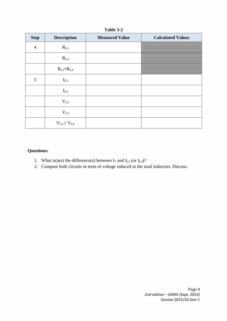
Table 3-2
Step Description Measured Value Calculated Values
4 RL3
RL4
RL3+RL4
5 IL3
IL4
VL3
VL4
VL3 // VL4
Questions:
1. What is(are) the difference(s) between IT and IL3 (or IL4)?
2. Compare both circuits in term of voltage induced at the total inductors. Discuss.

2018/2019 – Semester 1 Page 1
MALAYSIA-JAPAN INTERNATIONAL INSTITUTE OF
TECHNOLOGY
ELECTRONIC ENGINEERING LABORATORY I
(SMJE 1062)
2018/2019 – SEMESTER 1
LABORATORY SHEET
FUNDAMENTAL OF ELECTRICAL CIRCUITS
(UNIT 3)

2018/2019 – Semester 1 Page 2
FUNDAMENTAL OF ELECTRICAL CIRCUITS
LABORATORY SHEET 3
CAPACITANCE AND CAPACITIVE REACTANCE

2018/2019 – Semester 1 Page 3
TOPICS
1. CAPACITANCE
2. CAPACITIVE REACTANCE
OBJECTIVES:
1. To describe the effect a capacitor has on dc and ac circuits by using measured values
2. To determine the characteristics of resistive-capacitive (RC) circuits by using an
oscilloscope
3. To determine capacitive reactance (XC) by using calculated and measured values
MATERIALS REQUIRED:
1. F.A.C.E.T Base Unit
2. Virtual Oscilloscope
3. AC 1 Fundamental circuit board
4. RC TIME CONSTANTS circuit block
5. CAPACITANCE/CAPACITIVE REACTANCE circuit block
6. Virtual Generator
7. Power Supply, 15 Vdc
8. Multimeter

2018/2019 – Semester 1 Page 4
EXPERIMENT 1: CAPACITANCE
Objective:
To describe the effect a capacitor has on dc and ac circuits by using measured values
Procedure:
1. Turn off the power sources. Insert the AC 1 FUNDAMENTALS circuit board into the
base unit. Turn on the power sources.
2. Locate the RC TIME CONSTANTS circuit block, and connect the circuit shown in
Figure 1. Set up the oscilloscope for operation, and set the vertical coupling for
channels 1 and 2 to DC.
3. Switches S1 and S2, which are normally open, must be pushed and held in order to be
closed.
4. Use the multimeter to measure the voltage across capacitor C1. If you measure a
voltage, then C1 has a charge on it. Switch S2 provides a means of discharging C1
through R3. Press S2 for several seconds until 0 V is measured across C1.
5. Switch S1 applies the 15 Vdc to the circuit. While monitoring the oscilloscope for
voltage across capacitor C1, close (press) S1 and hold it closed. Does the capacitor
charge up to 15 V when the dc voltage is applied? Write down your observation in
Table 1.
6. Hold S1 closed for approximately 15 seconds. To remove the dc source from the
circuit, open (release) S1 while observing the voltage across C1. Does the charge on
capacitor C1 remain even after the dc source is removed? Is the charge is constant,
decreasing or increasing? Write down your observation in Table 1.
7. Discharge the capacitor by pressing S2 until the voltage across C1 is zero. Remove
the oscilloscope probe from the circuit.
8. Set the multimeter to read dc current. Replace the two-post connector between S1 and
R2 with the multimeter probes. Set the range of the multimeter to read microamps
(µA).
9. While monitoring the multimeter display, close S1 and hold it closed for about 15
seconds. Based on the reaction of the multimeter display, was current flowing while
capacitor C1 was charging? Write down your observation in Table 1. Discuss why the
current is flowing.
10. Based on the reaction of the multimeter display, observe whether the current flowing
or not after the capacitor became fully charged. Write down your observation in Table
1.
11. Locate the CAPACITANCE/CAPACITIVE REACTANCE circuit block, and connect
the circuit shown in Figure 2. Set the vertical coupling controls for both channels to
AC.
12. Use the oscilloscope to adjust VGEN for a 10 Vpk-pk, 1 kHz sine wave.
13. Measure and record circuit current (I) by using current-sensing resistor R2. Record
the result in Table 1.
14. Based on the result of Step 13, does the current flowing in the circuit indicate that
capacitor C3 is passing ac? Write down the discussion in Table 1.
15. Measure and record the voltage drop across C3 (VC3). Record the result in Table 1.
16. Using the value of I in Step 13 and the value of VC3 in Step 15, determine and record
the impedance of capacitor C3 (ZC3 = VC3/I). Record the value in Table 1.

2018/2019 – Semester 1 Page 5
17. Even though capacitor C3 is passing ac, is C3 presenting opposition to current flow?
Write down the discussion in Table 1.
18. Monitor the circuit current on the oscilloscope by observing the voltage across
current-sensing resistor R2. While observing the oscilloscope display, place CM
switch 10 in the ON position to increase the capacitance of C3 to 0.2 µF. Observe the
change in circuit current when the capacitance is increased. Write down in Table 1.
19. Return CM switch 10 to the OFF position. Increase the generator frequency while
observing the circuit current on the oscilloscope. Observe the change in current
current when the frequency is increased. Write down in Table 1
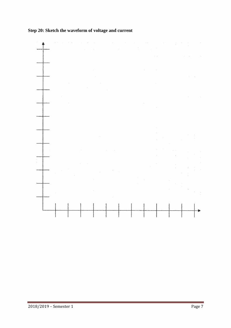
20. Readjust the generator frequency to 1 kHz. Connect the channel 1input of the
oscilloscope to measure VC3 and the channel 2 input to measure VR2 (circuit current
and VR2 have identical phase). Measure and record the phase angle ( ) between the
circuit current and VC3 (use VC3 as the reference). Does the circuit current lead or lag
the capacitor voltage? Sketch the waveform of voltage and current. Write down the
discussion in Table 1.
21. Turn off the power source.
Figure 1 Capacitor test circuit with dc source
Figure 2 Capacitor test circuit with ac applied

2018/2019 – Semester 1 Page 6
Result:
Table 1
No. Step Description Value/Answer
1 5 Does the capacitor charge up when the
dc voltage is applied?
YES/NO
2 6 Does the charge on capacitor C1
remain even after the dc source is
removed?
YES/NO
3 9 Was current flowing while capacitor
C1 was charging?
YES/NO
Discussion:
4 10 Current flowing
5 13 Circuit current (I)
6 14 Does the current flowing in the circuit
indicate that capacitor C3 is passing
ac?
YES/NO
Discussion:
7 15 Voltage drop across C3 (VC3)
8 16 Impedance of capacitor C3(ZC3)
9 17 Is C3 presenting opposition to current
flow YES/NO
Discussion:
10 18 Change in circuit current (Increased
Capacitance)
11 19 Change in circuit current (Increased
Frequency)
12 20 Phase angle ( )
13 20 Does the circuit current lead or lag the
capacitor voltage? Discussion:
2018/2019 – Semester 1 Page 7
Step 20: Sketch the waveform of voltage and current

2018/2019 – Semester 1 Page 8
EXPERIMENT 2: CAPACITIVE REACTANCE
Objective:
To determine the characteristics of resistive-capacitive (RC) circuits by using an
oscilloscope
To determine capacitive reactance (XC) by using calculated and measured values
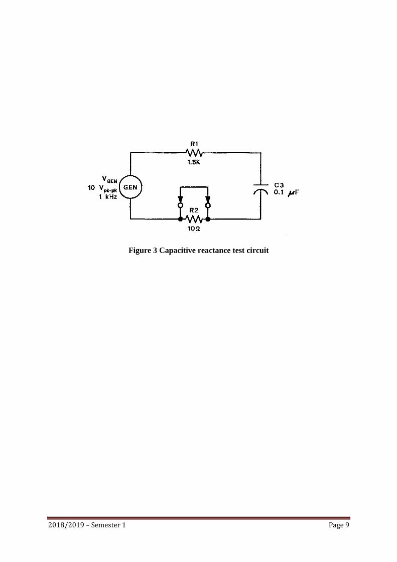
Procedure:
1. Turn off the power sources. Insert the AC 1 FUNDAMENTALS circuit board into the
base unit. Turn on the power sources.
2. Locate the CAPACITANCE/CAPACITIVE REACTANCE circuit block, and connect
the circuit shown in Figure 3. Adjust VGEN for a 10 Vok-pk. 1 kHz sine wave
(remember to set the frequency and amplitude with the oscilloscope). Calculate and
record the capacitive reactance of capacitor C3 (XC3 = 1/2 C).Record the value in
Table 2.
3. Measure and record the total circuit current (I) by using current sensing resistor R2 (I
= VR2/R2). Record the value in Table 2.
4. Measure and record the voltage drop across capacitor C3 (VC3). Record the value in
Table 2.
5. Use I and VC3 to determine the measured value of capacitive reactance XC3 (X C3
(measured) = VC3/I). Record your result in Table 2. Compare the measured value in
Step 4 with the calculated value in Step 2.
6. Place CM switch 9 in the ON position to decrease the value of C3 to 0.05 µF.
Readjust VGEN for 10 Vpk-pk if necessary. Calculate and record the new capacitive
reactance of C3 (XC3).
7. Measure I and VC3, and determine the new measured value of XC3.Record your result
in Table 2. Observe the change of capacitive resistance with decreasing capacitance.
Write down the discussion in Table 2.
8. Return CM switch 9 to the OFF position. Readjust VGEN for 10 Vpk.pk if necessary.
9. Decrease the frequency of the generator to 500 Hz. Remeasure I and VC3, and
determine the new measured value of XC3. Record your result in Table 2. Compare
this measurement with the initial XC3 measurement (Step 5). Write down the
discussion on the change of the capacitive reactance with decreasing frequency in
Table 2.
10. Readjust the generator frequency to 1 kHz. Decrease the amplitude of VGEN to 8
Vpk-pk. Measure I and VC3, and determine XC3. Record XC3 in Table 2.
11. Compare Step 10 with initial measurement (Step 5).Did XC3 increase, decrease, or
remain the same in relation to the initial value of XC3 measured? Write down your
observation and reason in Table 2.
12. Turn off the power source.
2018/2019 – Semester 1 Page 9
Figure 3 Capacitive reactance test circuit

2018/2019 – Semester 1 Page 10
Result:
Table 2
No Step Description Value/ Answer
1 2 XC3
(Calculated)
2 3 Total circuit current (I)
(Calculated)
3 4 Voltage drop across capacitor
C3 (VC3)
4 5 Measured XC3
(Initial Measurement)
5 5 Comparison of Step 2 and
Step 5
6 6 Calculated XC3
(Decreased Capacitance)
7 7 Measured XC3
(Decreased Capacitance)
I: VC3:
XC3
8 7 The change of capacitive
resistance with decreasing
capacitance
Discussion:
9 9 Measured XC3
(Decreased Frequency)
I: VC3:
XC3
10 9 Comparison of Step 9 and
Step 5
11 9 The change of the capacitive
reactance with decreasing
frequency
Discussion:
12 10 Measured XC3
(Decreased Amplitude)
I: VC3:
XC3
13 11 Observation on the change of
XC3
Reason/Discussion:
2018/2019 – Semester 1 Page 2 1st edition – MJIIT (Oct 2014) 2nd edition – KRS (Oct 2015)
MALAYSIA-JAPAN INTERNATIONAL INSTITUTE OF
TECHNOLOGY
FUNDAMENTAL OF ELECTRICAL CIRCUIT
(SMJE 1023)
2018/2019 – SEMESTER 1
FUNDAMENTAL OF ELECTRICAL CIRCUITS
LABORATORY SHEET 4
2018/2019 – Semester 1 Page 2 1st edition – MJIIT (Oct 2014) 2nd edition – KRS (Oct 2015)
SERIES AND PARALLEL RLC CIRCUITS
TOPICS
1. SERIES RLC CIRCUIT
2. PARALLEL RLC CIRCUIT
OBJECTIVES:
1. To measure current, voltage, total impedance, and phase angle in a series and parallel
RLC circuits
2. To observe and analyse voltage and current waveforms in series and parallel RLC
circuits
3. To observe the circuit behaviour with the change of capacitance and frequencies
LIST OF INSTRUMENTS:
1. F.A.C.E.T Base Unit
2. Virtual Oscilloscope
3. Virtual Generator
4. AC 2 Fundamental Circuit Board
5. Multimeter

2018/2019 – Semester 1 Page 2 1st edition – MJIIT (Oct 2014) 2nd edition – KRS (Oct 2015)
EXPERIMENT 1: SERIES RLC CIRCUIT
Objectives:
1. To measure current, voltage, and phase angle of a series RLC circuit
2. To observe voltage and current waveforms in a series RLC circuit
3. To observe the circuit behaviour with the change of frequencies
Procedure:
1. Insert the AC 2 FUNDAMENTALS circuit board into the base unit. Turn on the power
source.
2. Locate the RLC/RESONANCE/POWER circuit block. Connect the circuit shown in
Figure 1.
3. Adjust the sine wave generator frequency to 20 kHz and the voltage to 15 Vp-p.
4. Measure total circuit current (IT), VR2, VL1 and VC1. Record your results in Table 1.
5. Observe the waveform of the generator (VGEN) and total circuit current (IT). Sketch the
waveforms of VGEN and IT. Record the phase shift between VGEN and IT.
6. Adjust the generator frequency to 70 kHz.
7. Repeat Step 4 and 5.
8. Adjust the generator frequency to 20 kHz.
9. Varies the generator frequency until VGEN and IT are in phase. Record the frequency
value in Table 1.
10. Measure IT, VR2, VL1 and VC1. Record your results in Table 1.
11. Turn off the power source.
Figure 1 Series RLC Circuit

2018/2019 – Semester 1 Page 2 1st edition – MJIIT (Oct 2014) 2nd edition – KRS (Oct 2015)
Result:
Table 1
Step Description Measured Value
IT VR2 VL1 VC1
4 f = 20 kHz
5 Phase shift between VGEN and IT
7 f = 70 kHz
7 Phase shift between VGEN and IT
9 VGEN and IT are in phase Frequency, f =
10 VGEN and IT are in phase
Question (log book):
1. Discuss the effect of changing the frequency value on IT, VC1 and VL1 (Step 4 and 7)
2. Discuss the effect of changing the frequency value on phase shift between VGEN and IT.
3. Compare the current obtained in Step 4, 7 and 10. Discuss why the current is at
maximum when VGEN and IT are in phase.
Question (long report):
1. For each value of frequency, calculate IT, VR2, VL1 and VC1. Compare with the
measured values.
2. Compare the calculated values of phase shift between VGEN and IT with the measured
values.
3. Draw the phasor diagram for the measured values obtained in Step 5 and 7.
4. Compare the measured values of VGEN and VR2 when VGEN and IT are in phase. Discuss.
5. Compare the measured values of VL1 and VC1 when VGEN and IT are in phase. Discuss.
6. Calculate the frequency at which the reactance of inductor is equal to the reactance of
capacitor (XL = XC). Compare with the measured value.
7. Discuss why the current is at maximum when XL = XC.

2018/2019 – Semester 1 Page 2 1st edition – MJIIT (Oct 2014) 2nd edition – KRS (Oct 2015)
EXPERIMENT 2: PARALLEL RLC CIRCUIT
Objectives:
1. To measure current, voltage, and phase angle of a parallel RLC circuit.
2. To observe voltage and current waveforms in a parallel RLC circuit.
3. To observe the circuit behaviour with the change of frequencies
Procedure:
1. Connect the circuit shown in Figure 2. Turn on the power source.
2. Adjust the sine wave generator frequency to 20 kHz and the voltage to 15 Vp-p.
3. Measure IT, IR6, VR4 and VR5. Record your results in Table 2.
4. Calculate IC2 and IL2. Record your results in Table 2.
5. Observe the waveform of VGEN and IT. Sketch both waveforms. Record their phase
shift.
6. Adjust the frequency of the generator to 50 kHz.
7. Repeat Step 3, 4, and 5.
8. Adjust the generator frequency to 20 kHz.
9. Varies the generator frequency until VGEN and IT are in phase. Record the frequency
value in Table 2.
10. Measure IT, IR6, VR4 and VR5. Record your results in Table 2.
11. Calculate IC2 and IL2. Record your results in Table 2.
12. Turn off the power source.
Note: Current IC2 and IL2, can be found by measuring the voltage across R4 and R5
respectively.
Figure 1 Series RLC Circuit

2018/2019 – Semester 1 Page 2 1st edition – MJIIT (Oct 2014) 2nd edition – KRS (Oct 2015)
Result:
Table 2
Step Measured Value Calculated Value
IT IR6 VR4 VR5 IC2 IL2
3
4
5 Phase shift between VGEN and IT
7
7
7 Phase shift between VGEN and IT
9 Frequency when VGEN and IT are in phase
10
11
Question (log book):
1. Discuss the effect of changing the frequency value on IT, IR6, IC2 and IL2.
2. Discuss the effect of changing the frequency value on phase shift between VGEN and IT.
3. Compare the current IT obtained in Step 3, 7 and 10. Discuss why the current is at
minimum when VGEN and IT are in phase.
Question (long report):
1. For each value of frequency, calculate IL2, IC2, IR6 and IT. Compare with the measured
values.
2. Compare the calculated values of phase shift between VGEN and IT with the measured
values.
3. Draw the phasor diagram for the measured values obtained in Step 5 and 7.
4. Compare the values of IL2 and IC2 when VGEN and IT are in phase. Discuss.
5. Calculate the frequency at which the reactance of inductor is equal to the reactance of
capacitor (XL = XC). Compare with the measured value.
6. Discuss why the current is at minimum when XL = XC.

2018/2019 – Semester 1 Page 1 Edited by SAMA
MALAYSIA-JAPAN INTERNATIONAL INSTITUTE OF
TECHNOLOGY
ELECTRONIC ENGINEERING LABORATORY I
(SMJE 1062)
2018/2019 – SEMESTER 1
FUNDAMENTAL OF ELECTRICAL CIRCUITS
LABORATORY SHEET 5

2018/2019 – Semester 1 Page 2 Edited by SAMA
TOPICS
1. HIGH PASS FILTER
OBJECTIVES:
To demonstrate the operation of RC and RL high pass filters
To calculate and measure the cut-off frequencies and attenuation rates of RC and RL
high pass filters
To observe the relationship between cut-off frequencies and capacitance/inductance in
RC and RL high pass filters
MATERIALS REQUIRED:
1. F.A.C.E.T Base Unit (Power Supply, 15 Vdc)
2. Virtual Oscilloscope
3. Virtual Generator
4. AC 2 Fundamental circuit board
5. HIGH PASS FILTER circuit block

2018/2019 – Semester 1 Page 3 Edited by SAMA
EXPERIMENT 1: RC HIGH PASS FILTER
Procedure:
1. Insert the AC 2 FUNDAMENTALS circuit board into the base unit. Locate the HIGH
PASS FILTER circuit block on the AC 2 FUNDAMENTALS circuit board. Connect
the RC high pass circuit as shown in Figure 1. Turn on the power sources.
2. From the values given in Figure 1, calculate cut-off frequency, fCO [fCO= 1/(2πRC)].
Record the result in Table 1-1.
3. Set the generator for a 15 Vpk-pk, 100 kHz sine wave. Vary the generator frequency
over the 100 kHz to 100 Hz range while observing the filter output voltage across R2
(VR2). Repeat several times so that you can see how voltage changes with frequency.
Write down your observation on the change of VR2 with a decrease in frequency in
Table 1.
4. Complete Table 1 by adjusting the frequencies at the generator. Compute the dB
values from the expression dB = 20 log (VR2 at f / VR2 at 100 kHz). Record the value
in Table 1.
5. Calculate and record the output voltage level at the 3 dB down point.
(V-3dB = VR2 at 100 kHz × 0.707).
6. By varying the frequency of the generator, adjust your filter output voltage to the
V-3dB value that was obtained in step 5. This is the value of cut-off frequency, fCO.
Complete the missing values in Graph 1.
7. Refer to Graph 1; determine the attenuation difference (in dB/decade) obtained
between 500 Hz and 5 kHz. Record your answer in Table 1-2.
8. Repeat Step 3 to Step 7 by setting the CM switch 14 in the ON position to change the
value of C1 to 0.005 µF. Prepare your own table and graph for your answer.
9. Turn CM switch 14 to the OFF position. Switch off the power source.
Figure 1: RC high pass filter

2018/2019 – Semester 1 Page 4 Edited by SAMA
Results:
Table 1-1. Result for circuit with C = 0.01 µF
Step Description Value/Observation
2
Calculated cut-off
frequency, fCO
[fCO = 1/(2πRC)]
3
The change of VR2 with
decreasing frequencies
4 VR2 at each frequency
Table 1
FREQUENCY VOUT (VR2) dB DOWN
100 kHz
5 kHz
500 Hz
5
Output voltage level at the
3 dB down point.
(V-3dB = VR2 at 100 kHz ×
0.707)

2018/2019 – Semester 1 Page 5 Edited by SAMA
Table 1-2. Result for circuit with C = 0.01 µF
Step Description Value/Discussion
6
Graph 1 Response curve of an RC circuit
7 Attenuation difference (dB/decade):
Discussion:
1. Compare the attenuation difference value obtained in the experiment with the
theoretical value. Discuss.
2. What is the effect of changing the capacitor values in RC high pass filter circuit?
Discuss.

2018/2019 – Semester 1 Page 6 Edited by SAMA
EXPERIMENT 2: RL HIGH PASS FILTER
Procedure:
1. Locate the HIGH PASS FILTER circuit block on the AC 2 FUNDAMENTALS
circuit board. Connect the RL high pass circuit as shown in Figure 2. Turn on the
power sources.
2. From the values given in Figure 2, calculate fCO [fCO = R /(2πL)]. Record the result in
Table 2-1.
3. Set the generator for a 15 Vpk-pk , 100 kHz sine wave. Vary the generator frequency
over the 100 kHz to 1 kHz range while observing the filter output voltage across L1
(VL1). Write down your observation in Table 2-1.
4. Calculate the output voltage level at the 3 dB down point (V-3dB = VL1 at 100 kHz ×
0.707). Record the value in Table 2-1.
5. By varying the frequency of the generator, adjust your filter output (VL1) to the
computed value of V-3dB in Step 4. Measure the output period of the generator.
Convert this value to frequency to get fCO and record the value in Table 2-1.
6. By using the fCO measured value in step 5, determine in dB the amount of attenuation
(loss) of a frequency one octave lower than the cut-off frequency (fCO). Record the
value in Table 2-1.
7. Repeat Step 2 to Step 6 by setting the CM switch 15 in the ON position to change the
value of L1 to 20 mH. Prepare your own table and graph for your answer.
8. Turn CM switch 15 to the OFF position. Switch off the power source.
Figure 2: RL high pass filter

2018/2019 – Semester 1 Page 7 Edited by SAMA
Results:
Table 2-1. Result for circuit with L = 10 mH
Step Description Value/Observation
2
Calculated cut-off
frequency, fCO
[fCO = R/(2πL)]
3
The change of VL1
with decreasing
frequencies
4
Output voltage level
at the 3 dB down
point (V-3dB = VL1 at
100 kHz × 0.707)
5 Cut-off frequency, fCO
Output period:
Cut-off frequency:
6
The amount of
attenuation of a
frequency that is one
octave lower than the
cut-off frequency.
dB
Discussion:
1. Compare the attenuation difference value obtained in the experiment with the
theoretical value. Discuss.
2. What is the effect of changing the inductor in RL high pass filter circuit? Discuss.
3. What is the difference between using the RC high pass filter and the RL high pass
filter?