electronics lab manual - ucf...
TRANSCRIPT

A Manual explaining the basic Components, Devices and
Experimental Methods employed in an Electronic
Instrumentation Lab for Scientists.
MULTIMETER.
Digital Multi Meters (or DMMs abbreviated) and Digital Volt Meters (or DVMs
abbreviated) have replaced analog meters foe measuring voltages, currents and
resistances. The multi meters we are using have various input jacks that accept banana
plugs and one can connect the meter to the circuit under test using two banana plug leads.
Depending on how we configure the meter and its leads we can measure:
The voltage difference between the two leads.
The current flowing through the meter from one lead to the other
The resistance connected between its leads.
Multi meters usually have a selector knob, which allows us to select what is to be
measured and to set the full scale range of the display to handle inputs of various size.
To avoid damaging the circuit before you power up the circuit under test, set the meter at
its highest scale to avoid overflowing it.
THE BREADBOARD.
Breadboards are tools that help us build and test electric circuits. They include not only
sockets for plugging in components and connecting them together, power supplies, a
function generator, switches, logic displays etc.

Illustration showing many of the basic features of a breadboard with internal
connections shown for clarity. Note that each vertical column is broken into halves
with no built in connection between the top and the bottom.
The breadboard sockets contain spring contacts. If a wire is pushed inside a socket the
contacts press against it making an electrical connection. The sockets are internally
connected in groups of five (horizontal rows) or groups of twenty five (vertical columns).
Each power supply connects to a banana jack and also to a row of sockets running along
the to edge of the unit. The three supplies +5Volts (red jack in some breadboards), +15
Volts (yellow jack in some breadboards) and –15 Volts (blue jack in some breadboards)
have a common ground connection (black jack). The +15V and –15V supplies are
actually adjustable using the knobs provided, from less than 5V to greater than 15V.

MEASURING VOLTAGE
Voltage is always measured with respect to something usually a local ground (the
breadboard ground).
When connecting things is always a good idea to use color coding to help keep track of
which lead is connected to what. Use a black banana lead to connect to the “common”
input of the meter to the “ground” jack of the breadboard. Use a red banana plug with the
“V” input of the meter. Since the DMM is battery powered it is said to “float” with
respect to ground. It is therefore possible to measure the voltage drop across any circuit
element by simply connecting the DMM directly across the element.
Measuring Voltage. (a) An arbitrary circuit diagram is shown as an illustration on how
to use a voltmeter. Note that the meter measures the voltage drop across both the
resistor and the capacitor. (they have identical voltage drops since they are connected
in parallel). (b) A drawing of the same circuit showing how the leads of the DMM
should be connected when measuring voltage. Notice how the meter is connected in
parallel with the resistor.
When you operate the multi-meter always start from the scale with the highest
maximum reading and then you proceed to a finer scale according to your readings.
You never start measuring current from the finest scale unless you want to burn its
fuse.
MEASURING ELECTRIC CURRENT.
Current is measured by connecting a current meter (an ammeter or a DMM in its current
mode) in series with the circuit element through which the current flows. Ohm’s law
relates the current I, voltage V and resistance R according to V = IR. (Notice that this is
not a universal law of electric conduction since not ever material exhibits the property of
linearity between the electric current passing through it and the voltage applied across it.
Materials with such a linear relationship are being used to fabricate “resistors”.

Measuring current. (a) Schematic diagram of a series circuit consisting of a power
supply a 10k potensiometer and a multimeter. (Notice that in this diagram the center
tap of the potensiometer is left unconnected. If we accidentally connect it to the power
supply or to the ground excessive current could flow and burn out the pot). (b) A
drawing of the same circuit showing how the DMM leads should be configured to
measure current. The meter is connected in series with the resistor.
In order to measure current it is necessary to break the circuit in order to connect the
ammeter in series to the element the current through which we want to measure. We also
need to ensure ourselves that indeed the same current we want to measure passes through
the ammeter as well.
This is demonstrated in the following examples. Notice the way the circuit has been
broken in order for the Ammeter to be inserted.
EXAMPLE 1:
In the above circuit the Ammeter measures the current supplied by the battery. It DOES
NOT measure the current through R1, R2 or R3 resistors, but the sum of these three
currents.

EXAMPLE 2:
In the circuit below the circuit has been broken in various parts and Ammeters have been
inserted. What current is each Ammeter measuring?
1) Ammeter A1 is measuring the (total) current supplied by the 12 Volt battery. You can
calculate this current by dividing the 12 Volts voltage by the net resistance seen by the
battery (R1 through R4 in parallel).
2) Ammeter A2 is measuring the current passing through the resistance R1.
3) Ammeter A4 is measuring the current passing through the resistance R2.
4) Ammeter A6 is measuring the current passing through the resistance R3.
8) Ammeter A7 is measuring the current passing through the resistance R4.
9) Ammeter A3 is measuring the current flowing from node X to node Y. This is the sum
of the currents flowing through resistances R2, R3 and R4. Therefore the reading of A3
should be equal to the sum of the readings of A4 plus A6 plus A7 or the sum of the
readings A4 plus A5.
10) Ammeter A5 is measuring the current flowing from node Y to node Z. This is the
sum of the currents flowing through resistances R3 and R4. Therefore the reading of A5
should be equal to the sum of the readings of A6 plus A7.

EXAMPLE 3:
In the figure above we can see the implementation of the electronic schematic on the left
with actual components and measuring devices on the right. Notice how the circuit is
broken and the Ammeter inserted in series with the resistor. The current flowing through
the Ammeter (and measured by it) is the same current flowing through the resistor.
Caution: You need to be CAREFULL when you measure ELECTRIC CURRENT.
There is a fuse inside the instrument to protect it from being destroyed. The fuse will
burn itself if the multi-meter draws more current than the maximum allowed. Since the
resistance of the multi-meter in Current measuring mode (ammeter) is very small, if
the current you try to measure is larger than the maximum reading of the scale the
fuse will burned and you will not be able to use it until we change it. When you operate
the instrument as an ammeter always start from the scale with the highest maximum
current reading and then you proceed to a finer scale according to your readings. You
never start measuring current from the finest current measuring scale unless you want
to burn its fuse.

THE EXPERIMENTS THAT YOU WILL DO ARE NOT
DESIGNED TO PROTECT YOUR INSTRUMENTS
FROM OVERLOADING. PLEASE READ CAREFULLY
THE NEXT STATEMENTS.
WHEN YOU MEASURE AN ELECTRIC CURRENT
BEFORE YOU TURN THE POWER ON ENSURE
YOURSELVES THAT:
1. THE MULTIMETER IS SET AT THE (AC OR DC)
CURRENT MEASURING MODE AND THAT IS AT
THE LARGEST CURRENT SCALE. IF YOU
OVERLOAD THE INSTRUMENT THE FUSE WILL
BURN ITSELF OFF SINCE THE INTERNAL
RESISTANCE OF THE IDEAL AMMETER IS 0.
2. YOU HAVE CONNECTED THE AMMETER IN
SERIES WITH THE ELEMENT THE CURRENT
THROUGH WHICH YOU WANT TO MEASUER. IF
THE CONNECTION IS ACCIDENTALLY IN
PARALLEL THE FUSE OF THE INSTRUMENT WILL
BURN ITSELF OFF SINCE YOU WILL SHORT THE
ELEMENT BECAUSE OF THE LOW INTERNAL
RESISTANCE OF THE AMMETER.

MEASURING RESISTANCE.
Resistances usually are little cylinders of carbon, carbon film, metal film or wound up
wire encased in an insulating coating with wire leads striking out the ends. Often the
resistance is indicated by means of color stripes according to the resistor color code.
Resistors come in various sizes according to their power rating. The common sizes are
1/8 W, ¼ W, ½ W, 1 W and 2 W.
The resistance in Ohms is the sum of the values in columns 1 and 2 multiplied by the
value in column 3 plus or minus the tolerance in column 4. For example the color code
for an 1kΩΩΩΩ resistor would be “brown-black-red”, for a 51ΩΩΩΩ “green-brown-black”, for a
330ΩΩΩΩ “orange-orange-brown”, etc.

A potentiometer is a special type of resistor that has an adjustable “center-tap” or
“slider”, allowing electrical connections to be made not only at the two “ends”, but also
at an adjustable point along the resistive material. The voltage of this adjustable point
depends on the setting of the potentiometer’s knob. Warning: If you accidentally connect
power or ground to the potentiometer’s center tap, you can easily burn it out rendering it
useless. If in doubt have someone check your circuit before turning on the power.
MEASURING CURRENT WITH A VOLTMETER.
We can use a Voltmeter to measure the current passing through a resistance. First,
measure the resistance and then measure the voltage drop across the resistance with the
voltmeter. Finally use Ohm’s law to find out the current. This technique is very useful
when the ammeter fuse is burned and we cannot measure (especially small) currents
directly. We can use this technique only with resistances not with dynamic elements like
diodes or transistors.
CAPACITOR VALUE CODING
For some type of capacitors their value (and units) appear explicitly written on their
bodies. Other types of capacitors have their value encoded using color code.
Certain types of small capacitors (polyester, ceramic or mylar) capacitors have their
value written on them. On their body their written value is encrypted in a three digit
number . The first two digits indicate the first two most significant digits of their
numerical value. The third digit indicates the number of zeros after the two most
significant digits. The numerical value that appears this way is in pico Farads.
Example: Suppose you see the number
324 printed on the body of the capacitor.
The numerical value of the Capacitance
indicated is:
320000 pF or 320 nF or 0.32 µF
Next to the numerical value of the
capacitor a letter is usually printed
indicating the tolerance of the capacitor. Here are some tolerances and the corresponding
letters

%80%20%,50%20%,0%100
%20%,10%,5,5.0,25.0
+−=+−=−+=
±=±=±=±=±=
ZYP
MKJpFDpFC
THE PROBE
Oscilloscopes come with probes. Probes are cables that have a coaxial connector on one
end for connecting to the oscilloscope and a special tip on the other for connecting to any
desired point of the circuit to be tested. Top increase the scope’s input impedance and
affect the voltage to be measured as little as possible we can use a “10X” attenuating
probe which has circuitry inside that divides the signal voltage by 10. Some oscilloscopes
sense the nature of the probe and automatically correct for this factor of 10; other
oscilloscopes need to be told by the user which attenuation setting is in use. Note that a
probe has an alligator clip that connects to the shield of the coaxial cable (ground) which
is useful in reducing noise when probing high frequency or low voltage signals. Since it
is connected directly to the scope’s case, which is grounded via the third prong of the AC
power plug, it must be never allowed to touch any point of a circuit other than the
ground. Otherwise you will create a short circuit, which could damage circuit
components. This is no problem if you are measuring a voltage with respect to ground.
But if you want to measure a voltage drop between two points in the circuit neither of
which is at ground, first observe one point then observe the other. The difference between
the two measurements is the voltage drop across the element. During this process the
alligator clip of the probe should always be attached firmly to ground.
An attenuating probe can distort a signal. The manufacturer therefore provides a
“compensation adjustment” screw, which needs to be tuned for minimum distortion
An oscilloscope should have built in a calibration circuit that outputs a standard square
wave you can use to test a probe. Display the calibration square wave signal on the scope.
If the signal looks distorted carefully adjust the probe compensation using a small
screwdriver.

THE OSCILLOSCOPE
Illustration of a typical digital oscilloscope. The basic features to be used are shown.
Note the location of the AUTOSET button. When everything else fails try “autoset”.
Vertical controls.
There is a set of vertical controls for each oscilloscope channel. These adjust the
sensitivity (Volts per vertical division on the screen) and offset (the vertical position of
the beam on the screen when the input voltage is 0). The “CH1” and “CH2” menu
buttons can be used to turn the display of each channel on and off. They also select,
which control settings are programmed by the push buttons to the right of the screen.
Horizontal sweep.
To the right of the vertical controls there are the horizontal controls. Normally the scope
displays voltage on the vertical axis and time on the horizontal. The SC/DIV knob sets
the sensitivity of the horizontal axis (time per horizontal division on the screen). The
POSITION knob moves the image horizontally on the screen.
Triggering.
Triggering is the most complicated function performed by the scope. To create a stable
image of a waveform the scope must “trigger” its display at a particular voltage known as
the trigger “threshold”. The display is synchronized whenever the input signal “crosses”
that voltage, so that many images of the signal occurring one after another can be

superimposed on the same place on the screen. The LEVEL knob sets the threshold
voltage for triggering. One can select whether triggering occurs when the threshold
voltage is crossed from below (rising edge triggering) or from above (“falling-edge”
triggering) using the trigger menu (or for some scope models using trigger control knobs
and switches). You can also select the signal source for the triggering circuitry to be
channel 1, channel 2, an external trigger signal or the 120 V AC power line.
Setting up the trigger can be tricky, that is why some oscilloscope models provide an
automatic set-up feature (via the AUTOSET button) which can lock in on any repetitive
signal presented at the input and adjust the voltage, the time sensitivities and the
triggering for a stable display.
GROUNDING.
We must be very careful when we ground various instruments. Although it is not very
clear when we look at the schematics, the output (or input) lead of the instrument labeled
as ground is also connected to the instrument case (chassis) as well as to the ground of
the power outlet. In the long run do not forget that there should be only one ground.
When we connect two instruments together we must ensure ourselves that the grounds
are also connected properly. Let us look at the following figure below.
A technician is attempting to display the voltage drop across the element labeled X at an
oscilloscope. He connects the ground of the probe to point B but since the grounds of the
two instruments are connected together (via the outlet ground), he essentially shorts
element Y (points B and G are forced to be at 0 Volts). The technician should find a
different way to display the voltage drop across element X.

TESTING DIODES.
Diodes exhibit low resistance and allow current to flow through them when forward
biased. When diodes are reverse biased they do not allow electric current to flow through
then and exhibit very high (practically infinite) resistance. In order to test a diode with a
multimeter we have to test it separately in the forward conducting and in the reverse
blocking mode.
In order to test the diode in the conducting forward mode with the multimeter we connect
the positive lead of the meter to the anode and the negative lead to the cathode of the
diode. For a normal Silicon diode the multimeter should display a low voltage of about
0.7 Volts, or a low resistance (between 1 and 30 Ohms).
To check the diode in the blocking mode connect the positive lead of the meter to the
cathode and the negative lead to the anode of the diode. The multimeter should display a
very high resistance (a thousand times the low resistance or an out of range reading).
Some multimeters have a special setting for diode testing. The experimental setup is
shown below.
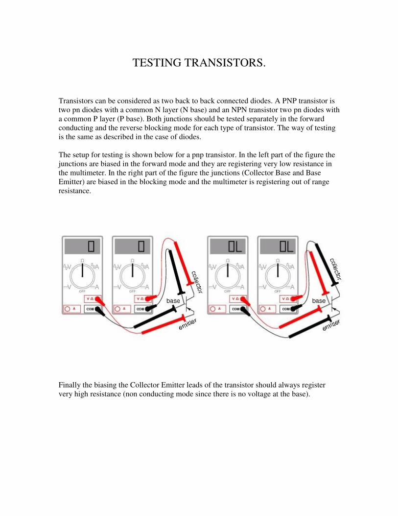
TESTING TRANSISTORS.
Transistors can be considered as two back to back connected diodes. A PNP transistor is
two pn diodes with a common N layer (N base) and an NPN transistor two pn diodes with
a common P layer (P base). Both junctions should be tested separately in the forward
conducting and the reverse blocking mode for each type of transistor. The way of testing
is the same as described in the case of diodes.
The setup for testing is shown below for a pnp transistor. In the left part of the figure the
junctions are biased in the forward mode and they are registering very low resistance in
the multimeter. In the right part of the figure the junctions (Collector Base and Base
Emitter) are biased in the blocking mode and the multimeter is registering out of range
resistance.
Finally the biasing the Collector Emitter leads of the transistor should always register
very high resistance (non conducting mode since there is no voltage at the base).

VOLTAGE SOURCES.
A voltage source (supply) is a device that forces a fixed voltage difference between the
leads of a load independent on the resistance of the load
RL. The current supplied by the voltage source is
calculated with the aid of Ohm’s Law and the resistance
of the load.
A practical Voltage Source has a small output
resistance r and can be approximated with an ideal
voltage source in series with the small output resistance
r of the non ideal supply.
A good voltage power supply must have an output
resistance much smaller than the load resistance in
order for the voltage appearing across the load to be
independent of the load itself.
Also a load that accepts an input signal in voltage form
must have a resistance much larger than the output
resistance of the signal source (voltage source).
Theoretically a voltage source must have zero output resistance and a load accepting a
signal in voltage form must have infinite resistance.
From the figure we can calculate the current delivered by the source and flowing through
the load:
Lout Rr
VI
+= and therefore the voltage across the load is:
VRr
RIRV
Lout
L
LL
+== a fraction of the voltage delivered by the source.
For 100% voltage delivery the load resistance RL must be much larger than the rout.
Ideally RL must be infinite and rout zero.

CURRENT SOURCES.
A current source (supply) is a device that delivers a fixed current difference at a load
independent on the resistance of the load RL.
The voltage appearing across the load (and
supplied by the current source) is calculated
with the aid of Ohm’s Law and the
resistance of the load.
A practical Current Source has a finite
output resistance Rout and can be
approximated with an ideal current source in
parallel with the output resistance Rout of the
non ideal supply.
A good current source must have an output
resistance much larger than the load
resistance in order for the current through
the load to be independent of the load itself
and to approach the current delivered by the
current source.
Moreover a load that accepts an input signal in current form must have a resistance much
smaller than the output resistance of the signal source (current source). Theoretically a
current source must have infinite output resistance and a load accepting a signal in
current form must have zero resistance.
From the figure we can calculate the voltage difference appearing between the leads A
and B of the load:
( )Lout
outL
LoutABRR
RIRRRIV
+== // and therefore the current flowing through the load is:
IRR
R
R
VI
Lout
out
L
AB
L
+== a fraction of the current delivered by the source.
For 100% current delivery on the load the load resistance RL must be much smaller than
the Rout. Ideally RL must be zero and Rout infinite.

VOLTAGE DIVIDERS.
A voltage divider is two resistors in series connected to a voltage source. Portion of the
voltage delivered by the source appears across
each resistance and therefore two resistances in
series constitute a practical way to supply to a
load a smaller voltage than the voltage delivered
by the source. The setup is illustrated at the
figure.
We can calculate the voltage difference between
points A and B by employing Kirchoff rules.
( )L
LRRR
VIRRRIV
////
21
21+
=⇒+=
and therefore the voltage delivered to the load is:
( )
+=⇒=
L
L
LLLRRR
RRVVRRIV
//
////
21
22
where L
LL
RR
RRRR
+=
2
22 //
We can see that the load resistance affects the operation of the voltage divider and
therefore the load voltage.

CURRENT DIVIDERS.
A current divider is two resistors in parallel connected to a current source. One of these
two resistors is the load. Only a portion of the current delivered by the source flows
through each resistance and therefore two
resistances in parallel constitute a practical
way to supply to a load a smaller current than
the one delivered by the source. The setup is
illustrated at the figure.
We can calculate the current flowing through
the load resistance RL by employing the rules
of Kirchoff. The voltage across the load is:
( )
+=⇒=
L
L
LLLRR
RRIVRRIV //
Therefore the current through the load is:
+=⇒=
L
L
L
L
LRR
RII
R
VI a fraction of the current delivered by the source. In practice
R contains the effects of the finite output resistance of the current source appearing in
parallel with any externally connected resistance to the source output.
THE THEVENIN EQUIVALENT CIRCUIT.
Consider an electronic device shown in the figure below. The device is shown as a “black
box” totally opaque to the user internally containing an unknown number and type of
electronic components. The complexity of the enclosed circuit is also unknown.
Terminals A and B interface the device with the external world and could serve either as
input or as output.
The Thevenin theorem states that the circuitry between terminals A and B internal to the
box can be replaced with the equivalent Thevenin circuit, a perfect voltage source
supplying a voltage called the Thevenin voltage (VTh) in series with a Resistance called
the Thevenin (sometimes called also the “input” or “output”) resistance depending on
weather terminals A and B serve as device input or output). The figure shows the
equivalent Thevenin circuit between terminals A and B replacing the internal components
of the device.

Rules for finding the Thevenin Voltage:
The Thevenin voltage (VTh) is the voltage difference between the terminals A and B
when they are open (and therefore no current flows into our out from the device).
Here are some basic procedures to find the Thevenin Resistance:
Method 1:
Short Terminals A and B and measure the current flowing through shorted terminals A
and B, Ishort. This current is also called the Norton current IN. The Thevenin Resistance is
the Thevenin Voltage divided by the current through the shorted terminals A and B
short
Th
ThI
VR =
Method 2:
Replace all Voltage Sources with a closed switch (short) and all Current Sources with an
open switch. The equivalent net resistance “seen” between terminals A and B is the
Thevenin Resistance.
Method 3:
Suppose you want to measure the input (or output) Resistance of a device. Ground the
output (or input if you are measuring the output resistance) and plug an ideal voltage or
current source at the terminal. Calculate the current supplied by the hypothetical ideal
voltage source or the voltage supplied by the hypothetical ideal current source if you
decide to go with a current source. Use Ohm’s law to calculate the resistance seen by the
source between the terminals.

Method 4:
Measure with a voltmeter the voltage between the terminals A and B. The voltmeter has
infinite resistance (it draws no current from the device) and therefore it registers the
Thevenin Voltage. Plug a load variable resistance RL between the terminals A and B (use
a potensiometer for this). With a voltmeter measure now the voltage drop across the load
resistor. With a screwdriver vary the value of the resistor until the voltmeter registers a
voltage drop across the load equal half the value of the already measured Thevenin
voltage. What is the relationship between the value of that load resistance and the
Thevenin Resistance between terminals A and B. Hint: The circuit is essentially a
voltage divider where the Thevenin Voltage is split on the Thevenin Resistance and on the
Load resistance.
THE NORTON EQUIVALENT CIRCUIT.
Consider the same electronic device shown in the figure below once more. The device is
again shown as a “black box” totally opaque to the user, internally containing an
unknown number and type of electronic components. The complexity of the enclosed
circuit is also unknown. Terminals A and B interface the device with the external world
and could serve either as input or as output.
The Norton theorem states that the circuitry between terminals A and B internal to the
box can be replaced with the equivalent Norton circuit, an ideal Current Source supplying
an electric current called the Norton (IN) in parallel with a Resistance called the Norton

(sometimes also called the “input” or “output”) resistance depending on weather
terminals A and B serve as device input or output.
The Norton Resistance RN is the same as the Thevenin Resistance discussed
above and therefore we already know how to find it (RN = RTh).
The figure shows the equivalent Norton circuit between terminals A and B
replacing the internal components of the device.
Rules for finding the Norton Current:
The Norton current is the current flowing through the terminals A and B if we short them.
(It is the Ishort current we used in the Thevenin theorem discussion to find the RTh).
USAGE OF NORTON AND THEVENIN CIRCUITS.
The Thevenin and Norton equivalent circuits are being used to determine how two
electrical or electronic components behave when they interact that is when they are
connected in such a way so that the output of the first becomes the input of the second.
Consider the situation shown in the figure below where device A (say a sensor or
detector) delivers its signal to device B (say an Amplifier). Device A is considered a
voltage source (the output information is supposed to be the voltage) and device B is a
voltage Amplifier (expects a voltage signal at its input). The output of device A (the
sensor) has been replaced with its equivalent Thevenin Circuit, there the Thevenin

voltage is the signal VS and the Thevenin Resistance is the output resistance of the
detector say Rd. The input of the amplifier has been replaced by its Thevenin rinput
Resistance say Rin. On the Amplifier input side there is no signal therefore there is no
Thevenin Voltage or Norton Current source.
We can recognize immediately the action of the voltage divider and the signal which
really appears at the input of the Amplifier and being Amplified is:
+ Din
in
SRR
RV
which is a fraction of the useful voltage delivered by the sensor.
For good “matching” of the two electronic devices we want this fraction to approach
100%, that is we need Rin to be much larger that RD. Ideally we want the voltage source
to have zero output resistance and the device accepting voltage signals to have infinite
input resistance.
Consider now the situation shown in the figure below where device A (say a sensor or
detector) delivers its signal to device B (say an Amplifier). However now device A is
considered a current source (the output information is supposed to be encoded in the form
of current) and device B is a current Amplifier (expects a current signal at its input). The
output of device A (the sensor) has been replaced with its equivalent Norton Circuit,
there the Norton Current is the signal IS and the Norton Resistance (same as the Thevenin
resistance) is the output resistance of the detector say Rd. The input of the amplifier has
been replaced by its Thevenin (or Norton) input Resistance say Rin. On the Amplifier

input side there is no signal therefore there is no Thevenin Voltage or Norton Current
source.
We can recognize immediately the action of the current divider and the signal which
really flows through Rin at the input of the Amplifier and therefore being Amplified is:
+ Din
D
SRR
RI
which is a fraction of the useful Current Signal delivered by the sensor.
For good “matching” of the two electronic devices we want this fraction to approach
100%, that is we need Rin to be much smaller that RD. Ideally we want the current source
to have infinite output resistance and the device accepting current signals to have zero
input resistance (effectively shorted inputs).
We see therefore that the practical usage of the Norton and Thevenin equivalent circuits
in electronics is to determine how two circuits interact when they are connected and
signals are propagating through them.
We can model the input and/or the output of a device either with its Norton or with its
Thevenin equivalent circuits. The Norton and the Thevenin resistances are the same ant
the Thevenin voltage is related to the Norton current via the formula:
ThNThNTh RRRIV ==
The results of our analysis will be the same and independent on our choice to model it
using the Thevenin or the Norton equivalent circuit.

However we need to decide if we will consider the output of a device a signal or a current
source based on the output resistance as well as we need to decide if the input of a device
is accepting signals in voltage or in current form base on its input resistance. It is the
responsibility of the experimentalist and the designer to make a good matching of the
components.
THE OPERATIONAL AMPLIFIER (Op Amp)
An Operational Amplifier (otherwise called op-amp) is a Differential Amplifier
incorporated in a chip as a linear integrated circuit. The Differential Amplifier is an
Amplifier which amplifies the
difference between two signals
applied to the two inputs it has. The
two inputs are indicated with the
symbols:
+ (plus) or the non inverting input or
υ+ and
-- (minus) or the inverting input or
υ--
The output signal can be written
as: ( )−+ −⋅= υυυ Aout
The gain A is a very large number
usually between 150,000 and
300,000.
In the figure we show the schematic diagram for an op amp as it appears in electronic
circuit designs.
The most widespread op-amp chip is the LM741
which incorporates a single amplifier per chip.
The experimentalist should always study the
data sheet of the LM741 chip for the correct
specifications and pin-out usage.
In order for the chip to work it needs to be
powered by a positive and a negative power
supply, indicated by +Vcc and –Vcc in the
figure. Their values need not be the same but for
most cases we select +12V and -12V (or +15V
and -15V). The pin out diagram appears in the
Figure. Pin NC is left unconnected. For basic lab experiments the OFFSET NULL pins
will be left unconnected too.

Note: The op-amp cannot deliver an output voltage outside the +Vcc and –Vcc
range. Also the op-amp cannot deliver an output current larger than a value
specified at its data sheet (15 mA or 20mA for the LM741 chip). The chip clips the
output voltage and the output current at their limit values.
The LM741 has been designed
to appear in linear Op-Amp
Circuits with negative
feedback. That is when we
design electronic circuits
involving the 741 op-amp a
portion of its output is fed at
the inverting input (negative
feedback), via passive elements
(usually Resistors and/or
Capacitors)
An example of such a circuit
appears in the figure.
In order to analyze such circuits we follow the following three Op-Amp rules:
Rule 1: The Op-Amp has infinite input impedance and no current is flowing into it.
Rule 2: The Op-Amp with a negative feedback at a linear electronic circuit works in such
a way so that, both inverting (minus) and non-inverting (plus) inputs are held at the same
voltage. For Example in the figure the inverting input is held at zero voltage (virtual
ground) by virtue of the non inverting input that is hardwired at the ground.
Rule 3: Rule number 2 does not hold if the output voltage or if the output current ar out
of their limits (their specs). They cannot be out of their limits. Simply the chip clips the
output voltage (or the output current) at their limiting values whatever the input voltages
at the inverting and non inverting inputs may be.
These rules allow us to analyze almost all linear circuits containing op amps and calculate
the output voltage as a function of the input (the gain for the circuit).