electronics digest 1980 winter - world radio history
TRANSCRIPT

DATA PIN OUTS • CHARACTERISTICS • INSTRUCTION SETS • GLOSSARY
SUBSCRIPT DICTIONARY • DATA SHEETS • COMPONENTS EXPLAINED EQUIVALENTS • TRUTH TABLES • CIRCUITS
•
,••••
•
VOL1 No 3 £1.50
•
—M,I
04.
a/
'41/11111111111111111t .'
'ir •
BO I( 100 Pages of invaluable info, for the electronics
and computing enthusiast.

INTRODUCTION Since we began publishing magazines in this country, over eight years ago, Modmags' aim has been to inform people who are interested in the ever-expand-ing field of electronics. Our first title, Electronics To-day International, with its vast range of constructional projects and up-to-date reports on the latest de-velopments in technology, was an incredible success. This led to the launching of two more magazines — Hobby Electronics, for the less experienced construc-tor and beginner in electronics; and Computing To-day, for people interested in home computing and small systems.
In all these magazines it has been our aim, not only to provide projects and programs for you to copy, but to help those who are more able and experienced to experiment for themselves. After all, that's half the fun of electronics! Our Electronic Circuit Design series covered the theoretical ground - now Electronics Digest No. 3 provides the information for those who want to get their hands dirty and their soldering irons tinned.
Transistors
The following tables provide all of the basic informa-tion that a designer requires when selecting tran-sistors for a specific application. Furthermore, the lead connections for each transistor are given in the table, to make life easier for people building up circuits with only a circuit diagram to work from. The transistors included in this table are virtually all
available from one or more of the major mail order companies. However, should any type prove difficult to obtain (or you need a transistor now and the shops are shut) then the information given here can be used as a guide to help you select a substitute. Bear in mind that this can only be an approximate guide, and you substitute at your own risk!
Computing This section is for the home computer enthusiast. Basic information is given on four of the most popular microprocessors, together with tables of their instruc-tion sets — conveniently laid out for the bewildered programmer. There are also brief surveys of each type of support chip, including RAMs, PROMs, dy-namic RAMs and I/O devices. The ASCII set is listed and there is a conversion table for hex to decimal and vice-versa.
General Information What are the different types of power supply circuit? How do I wire up an op-amp? What is an AND gate? Or an ALU? What does TTL stand for? Why aren't you looking up the answers in the glossaries and pages of data that we've collected together for you?
Components It may be possible to build projects without knowing anything about resistors and capacitors except that they're the little cylinders with wires sticking out of the ends, but it's not very satisfying. There are four articles in this issue which examtne different cate-gories of component and their construction. Perform-ance, cost and application are all considered, so that you can see why certain types are used in our circuits, and which ones you should use in yours.
Logic There are two main types of IC logic families, TTL and CMOS. They feature extensively in digital circuits and every home constructor should have access to pin-out tables. (Ever seen a circuit design you'd like to build, with no pin numbers marked? Frustrating, isn't it.) The tables also show the internal arrangement of the ICs to help you understand their function.
Data Sheet A selection of articles containing manufacturer's data on some popular ICs. Each IC has application circuits given, to be built as they stand or used as a basis for experiment. We've also included an article explaining the notation used in data sheets, as we've found that quite a lot of confusion exists as to what the data actually means (see the cautionary tale that starts off the article).
Digest No. 3 Whatever your interest in electronics, there's bound to be something in this magazine that you'll need to know sooner or later. If you still haver't decided to buy it, are you sure you're standing at the right rack in the newsagents?
2 Electronics Digest, Winter 1980/81

Editing and Production Ron Harris, B.Sc and Peter Green
Editorial Assistant Tina Boylan
Computing Consultant Henry Budgett
Group Art Editor Paul Wilson-Patterson
Drawing Office Manager Paul Edwards
Managing Director T. J. Connell
Distributed by: Argus Distribu-tion Ltd, 12-18 Paul Street, Lon-don. 01-247 8233. Printed by: QB Printers Ltd, Colchester. MODMAGS LTD 1980. All
material is subject to worldwide copyright protection. All reason-
able care is taken in the prepara-tion of the magazine, contents, but the publishers cannot be held responsible for errors legally. Where mistakes do occur, a cor-rection will normally be published as soon as possible afterwards. All prices and data contained in advertisements are accepted by us in good faith as correct at time of going to press. Neither the advertisers nor the publishers can be held respons-ible, however, for any variations affecting price or availability which may occur after the publi-cation has closed for press.
Audi Gener General pu General purpo
General purpo General purpo General purpo General purpo Audio, extra big
General purpo General purpo Audio, high General purpose General purpose
General pur-po General purpo RF, big Gener Audi
CONTENTS
INTRODUCTION Why you need this magazine 2
TRANSISTORS Pin connections 4
Electrical data 5
ABBREVIATIONS The short and the long of it 15
PROBLEMS? A few helpful hints 15
RESISTORS We couldn't resist this one 16
TTL Pinouts Make the logical connections 25
BASIC TRUTH TABLES Which gates do what 39
CMOS PINOUTS The same as TTL, only different 40
POTENTIOMETERS A turn for the better 44
OP-AMP CIRCUITS All the basic configurations 47
PSU CIRCUITS Transform your circuits 47
IC SURVEY See what's on offer 48
TL080 OP-AMP FAMILY A new generation 50
SN76477 Sound effects generator 52
DATA SHEETS EXPLAINED What do they really mean? 54
ICM 7217/7227 You can count on this 57
TDA 1008 Frequency divider for musicians 60
ICI 7106 One chip digital panel meter 62
ICL 8038 Waveform generator and VCO 64
CAPACITORS All you need to know 66
RF CHOKES Different styles and important parameters 74
8080 CPU 78
Z-80 CPU 80
6800 CPU 84
6502 CPU 86
AY-5-1013A A typical UART 88
MC14412 Versatile modem 90
STATIC RAM Information on the 2102, 2112, 2114 and 6810 92
DYNAMIC RAM The 4027 and 4116 ICs 93
PROMs We consider the 1702, 2704, 2708, and 2716 96
HEX CONVERSION Hex to decimal, and decimal to Hex 98
ASCII CODE SET For easy reference 98
MPU GLOSSARY Find out what we're talking about 99
Electronics Digest, Winter 1980 81 3

Explanation of Tables Type Manufacturer's code number. Pol/Mat Polarity of transistor and semiconductor material used. N is NPN; P is PNP; G is germanium; S is silicon. Case Style Refers to the lead connections shown be-low. Vcg (max) Maximum permissible collector-base voltage with the emitter open-circuit. VcE (max) Maximum permissible collector-emitter voltage with the base open-circuit. VEg (max) Maximum permissible emitter-base
voltage with the collector open-circuit. lc (max) Maximum permissible collector current — given in mA unless otherwise stated. PTOT (max) Maximum power dissipation of the device — given in mW unless otherwise stated. 11 FE (min) Minimum current gain of the device. As this depends to a large extent on the collector bias current at which measurements are made, the value is also listed (in mA unless otherwise stated). fr (min) Minimum frequency at which the common-emitter current gain will drop to unity — given in MHz. Application A guide (although necessarily limited) to the typical device application.
TO1 b
• e . TO1H b
. a e TO3
I c 0 lo , bo I 0 .
TO5
• e e
TO5a
a TO5F
lieeld>
TO7
C11)
TO12 b
e Illb
I
'
e
TO18 b
• ID e
T036 Locating pon
Il ° I ' b
1039 b
• lip c
'
1059 T060 T061 I T066 .—:---- i
0 •o , , 0
;
bo 1
Collector Connected to Base
° b 0 o •
0 0 b CI •be0
0
, T072 b
• diii, e s
' '
TO72a •
b e c s
T092
b . e b
TO92a • c b TO92b
e
•
TO92c
c
:II,
TO92d
cf • b
'
1092e
b •
C.
1) TO92f
b
c
si i
T098
c
e
b
10105 b
• e , TO105a
b . ge c TO106 b . e c
TO106a •
b 0 e
10126 e c b
7 0 t=t)
Mounting Surface
TOP3 b c e
TOP66 b c e
TOQ66 X01
a X 01a
<,,,, c. 0 ,
,.. , rczi t=1 :=1) ii=1Z) ,
Mounting Surface Mounting Surface C
X02
b e eo o
X03 e
I ito 1
l 0
bol i
X04 b
0 III) C
X09 b
X09a e
ia. 11.21.1à
I c
Élstl iià
b c
x10 •
C
X10a b
e
•
X11
b
•
X13
b e
111
X13a
idd:j.: e
X16
b e •
X17
rcle/ .1;i)
• b c
_
X27 c<ilu t.), =
• •
c
X37
• C=9=1 c Notes:
S= Shield (Case) Transistors are seen from be-
low
4 Electronics Digest, Winter 1980/81

TRANSISTORS
Type Pol Mat Case VCB VCE VEB 1c P10T h, (Tin) fr (min) Application Style (max) (max) (max) (max) (max) k (mA) MHz
V V V mA mW
AC107 PG X01 15 15 5 10 80 35 (à 300 1 Audio amplifier AC117 PG X04 32 18 10 1A 1W 40 (a 150 0.5 General purpose audio AC125 PG 7131 32 12 10 100 500 50 (a 2 1 Audio amplifier AC126 PG 701 32 12 10 100 500 100 (a 2 1 General purpose audio AC127 NG 701 32 12 10 500 340 SO (a 500 1.5 General purpose audio
AC128 PG 701 32 16 10 1A 267 45 ,, 1A 1 General purpose audio AC141 NG 701 32 18 10 1.2A 720 40 ,, 400 1 General purpose audio AC141K NG X04 32 18 10 1 2A 720 40 '' 400 0.5 General purpose audio AC142 PG 701 32 20 10 1 2A 720 40 a 400 1 General purpose audio AC142K PG X04 32 20 10 1 2A 860 40 (ii 400 0.5 General purpose audio
AC151 PG 701 32 24 10 200 900 30 (a 2 1 Audio amplifier AC152 PG 701 32 24 10 500 900 30 (a 100 1 General purpose audio AC153 PG 701 32 18 10 2A 1W 50 (a 300 1 General purpose audio AC176 NG 701 32 20 10 1A 220 52 (a 500 1 General purpose audio AC187 NG 701 25 15 10 2A 225 100 (a 300 1 General purpose audio
AC11,7K NG X04 25 15 10 2A 1W 100 (a 300 1 General purpose audio AC188 PG 701 25 15 10 2A 225 100 fa 300 1 General purpose audio ACI88K PG X04 25 15 10 2A 1W 100 ((( 300 1 General purpose audio ACY17 PG TOS 70 32 12 500 260 50 as 300 1 General purpose audio ACY18 PG 705 ' 50 30 12 500 260 40 (a 300 1 General purpose audio
ACY19 PG 705 50 30 12 500 260 80 (a 300 1 General purpose audio ACY20 PG TO5 40 20 12 500 260 50 (a 50 1 General purpose audio ACY21 PG TOS 40 20 12 500 260 90 (a 50 1 General purpose audio ACY22 PG 705 20 15 12 500 260 30 (a 300 1 General purpose audio ACY28 PG 701 40 15 30 200 200 45 (a 1 08 RF amplifier
ACY39 PG 705 110 40 25 500 260 50 (a 300 1 Audio, high voltage ACY40 PG 705 32 18 12 500 260 30 (a 300 1 General purpose audio ACY4I PG TOS 21 18 12 500 260 50 (a 300 1 General purpose audio ACY44 PG 705 50 30 12 500 260 40 (a 300 1 General purpose audio AD140 PG 703 55 55 10 3A 35W 30 (a 1A 0.2 General purpose audio
AD142 PG 703 80 50 10 10A 30W 30 (a 1A 0.45 Audio, high voltage AD149 PG TO3 50 30 20 3 5A 27W 30 ((i IA 0.2 General purpose audio AD150 PG 703 32 30 10 3 5A 27W 30 (a IA 0.45 General purpose audio AD161 NG X03 32 20 10 1A 4W 80 (a 500 I General purpose audio AD162 PG X03 32 20 10 1A 6W 50 (a 500 1 General purpose audio
AF106 PG 7072 20 15 0.3 10 60 25 (a 1 100 General purpose FM VHF AF109 PG 7072 25 18 0.3 12 60 20 (a 2 100 VHF amplifier AF114 PG 707 32 15 2 10 75 50 (a 1 75 RF amplifier AF118 PG 707 70 20 2 30 375 125 RF amplifier AF121 PG 701H 25 25 10 140 30 (a 3 270 VHF amplifier
AFI24 PG 7072a 32 15 2 10 75 50 (a 1 75 General purpose, RF AFI25 PG 7072a 32 15 2 10 75 50 (a 1 75 General purpose, RF AFI26 PG 7072a 32 15 2 10 75 50 (a 1 75 General purpose, RF AFI27 PG 7072a 32 15 2 10 75 50 (a 1 75 General purpose. RF AF139 PG 7072 20 15 0.3 10 60 10 (a 1.5 275 UHF amplifier
AF178 PG 7072 20 15 0.3 10 60 10 (à 1.5 275 UHF amplifier AFI80 PG 7012 25 25 25 156 10 .a 14 150 VHF amplifier AF186 PG 7012 25 0.5 15 100 20 a 1 50 FM VHF general purpose AF239 PG 7072 15 15 0.3 10 60 10 a 2 400 TV UHF oscillator AF279 PG X37 15 15 0.3 10 60 10 a 2 400 TV UHF gain controlled amplifier
AFZ11 PG 7072a 20 10 0.5 10 83 20 a 1 135 VHF amplifier ASY26 PG 705 30 15 20 200 150 30 ,i 100 4 RF switch ASY27 PG 705 25 15 20 200 150 30 , 100 6 RF switch ASY50 PG 701 20 10 20 200 200 15 ,, 5 04 RF amplifier ASY76 PG TO5 40 32 10 500 260 26 .a 300 1 General purpose audio
ASZ21 PG 7018 20 15 50 120 30 (a 10 300 VHF switch BC107 NS 7018 50 45 6 100 300 110 ai 2 150 General purpose audio BC107B NS 7018 50 45 6 100 300 200 (ii 2 150 General purpose audio BC107C NS 7018 50 45 6 100 300 450 (a 2 150 BC108 NS 7018 30 20 5 100 300 120 (u 2 150 General purpose audio
BC108B NS 7018 30 20 5 100 300 200 iii 2 150 General purpose audio BC108C NS 7018 30 20 5 100 300 420 (ii 2 150 General purpose audio BC109 NS 7018 30 20 5 100 300 180 (a 2 150 Audio, low noise BC109B NS 7018 30 20 5 100 300 200 (a 2 150 Audio, low noise BC109C NS 7018 30 20 5 100 300 420 (a 2 150 Audio, low noise
Bd 13 NS 10106 30 25 6 50 200 200 (a 1 60 Audio, low noise BC114 NS 70106 30 25 6 50 200 200 (a 1 60 Audio, low noise BCI15 NS 70105 40 30 5 100 300 80 (a 10 40 General purpose audio BCII6 PS 70105 45 40 5 100 300 35 (i'l 10 130 General purpose audio BC1I7 NS 70105 120 120 5 50 300 30 (a 30 60 Audio, high voltage
BC1I8 NS 70106 45 45 4 100 200 50 (a 5 200 General purpose audio BC119 NS 7039 60 30 5 1A 800 40 (a 150 40 General purpose audio BC123 NS X16 45 30 5 50 90 25 (a 250,A 20 Audio, low noise BCI32 NS 70106 30 25 6 200 200 60 (a 10 40 General purpose audio BC134 NS 70106 45 45 4 200 200 150 ai 10 200 General purpose audio
BC135 NS 70106 45 45 5 200 200 50 (a 10 200 General purpose audio BC136 NS 70105a 60 40 5 100 300 40 (a 10 60 General purpose audio BC137 PS 70105 40 40 4 600 300 40 (a 10 60 General purpose audio BC139 PS 7039 40 40 5 500 700 40 (a 100 100 General purpose audio BC140 NS 7039 80 40 7 1A 37W 40 a 100 50 General purpose audio
Electronics Digest, Winter 1980 ,81 5

Type Pol Mat Case VCB VCE VEB IC PTOT hr (min) fr (min) Application Style (max) (max) (max) (max) (max) qr lc (mA) MHz
V V V mA mW
BC141 NS TO39 100 60 7 1A 3.7W 40 @ 100 50 General purpose audio BC142 NS 1039 80 60 5 1A 800 20 @ 200 40 General purpose audio BC143 PS 1039 60 60 5 1A 800 20 @ 300 100 General purpose audio BC147 NS X09 50 45 6 200 250 110 @ 2 150 Audio amplifier BC147B NS X09 50 45 6 200 250 200 @ 2 150 Audio amplifier
BC148 NS X09 30 20 5 200 250 110 @ 2 150 Audio amplifier BC148B NS X09 30 20 5 200 250 200 @ 2 150 Audio amplifier BC148C NS X09 30 20 5 200 250 420 @ 2 150 Audio amplifier BC149 NS X09 30 20 5 200 250 200 @ 2 150 Audio, low noise BC149B NS X09 30 20 5 200 250 200 q 2 150 Audio, low noise
BC149C NS X09 30 20 5 200 250 420 @ 2 150 Audio, low noise BC153 NS 10106 40 40 5 100 200 50 @ 10 40 General purpose audio BC154 NS TO106 40 40 5 100 200 160 @ 10 40 Audio, low noise BC157 PS X09 50 45 5 100 300 70 @ 2 130 Audio amplifier BC158 PS X09 30 25 5 100 300 70 @ 2 100 Audio amplifier
BC159 PS X09 25 20 5 100 300 120 @ 2 100 Audio, low noise BC160 PS 1039 40 40 5 1A 3.2W 40 @ 100 50 General purpose audio BC161 PS T039 60 60 5 1A 3.2W 40 @ 100 50 General purpose audio BC167A NS 1092 45 45 6 100 300 120 @ 2 85 General purpose audio BC168C NS TO92 20 20 5 100 300 380 (a 2 85 General purpose audio
BC169C NS 1092 20 20 5 100 300 380 @ 2 85 Audio, low noise BC170 NS X10 20 20 5 100 300 35 @ 1 60 General purpose audio BC171 NS X10 45 45 6 100 300 125 (à 2 100 Audio, low noise BC172 NS X10 25 25 5 100 300 125 (à 2 100 General purpose audio BC173 NS X10 25 25 5 100 300 125 @ 2 150 Audio, low noise
BC177 PS 1018 45 45 5 100 300 70 @ 2 130 General purpose audio BC178 PS TO18 30 25 5 200 300 70 @ 2 100 General purpose audio BC179 PS TO18 25 20 5 50 300 70 @ 2 100 Audio amplifier BC181 PS X10a 40 25 5 200 300 60 @ 2 100 General purpose audio BC182 NS X10 60 50 5 20 300 120 @ 2 150 General purpose audio
BC182L NS 1092 60 50 5 200 300 120 (à 2 150 General purpose audio BC183 NS X10 45 30 5 200 300 120 (à 2 150 General purpose audio BC183L NS 1092 45 30 5 200 300 120 (a- 2 150 General purpose audio BC184 NS X10 45 30 5 200 300 240 (à 2 150 Audio, low noise BC184K NS X10 45 30 5 200 300 240 @ 2 150 Audio, low noise
BC184L NS 1092 45 30 5 200 300 240 @ 2 150 Audio, low noise BC186 PS TO18 40 25 5 100 300 40 @ 2 50 Audio amplifier BC187 PS 1018 30 25 5 100 300 100 @ 2 50 Audio amplifier BC205 PS 10106 20 20 5 100 300 75 @ 2 100 General purpose audio BC212 PS X10 60 50 5 200 300 60 (à 2 200 General purpose audio
BC212L PS 1092 60 50 5 200 300 50 à 2 200 General purpose audio BC213 PS X10 45 30 5 200 300 80 @ 2 200 Audio, low noise BC213L PS 1092 45 30 5 200 300 70 @ 2 200 General purpose audio BC214 PS X10 45 30 5 200 300 140 @ 2 200 General purpose audio BC214L PS 1092 45 30 5 200 300 125 (à,` 2 200 Audio, low noise
BC237 NS X10 50 45 6 100 300 110 @ 2 150 General purpose audio BC238B NS X10 30 20 5 100 300 200 @ 2 150 General purpose audio BC239 NS X10 30 20 5 100 300 200 @ 2 150 Audio, low noise BC250 PS X10 20 20 5 100 300 35 @ 1 100 General purpose audio BC251 PS 1092a 45 45 5 100 300 125 @ 1 100 General purpose audio
BC253 PS 1092a 20 20 5 100 300 125 @ 2 80 General purpose audio BC256 PS TO92a 64 64 5 100 300 125 @ 2 100 General purpose audio BC258 PS 1092 25 25 5 100 300 70 @ 2 130 General purpose audio BC260 PS 1018 20 20 5 100 300 35 @ 1 100 Audio amplifier BC261 PS 1018 45 45 5 100 300 125 (à 2 100 Audio amplifier
BC262 PS 1018 25 25 5 100 300 125 (a 2 100 Audio amplifier BC266 PS 1018 64 64 5 100 300 125 e 2 200 Audio amplifier BC266A PS TO18 64 64 5 100 300 125 (6' 2 200 Audio amplifier BC266B PS 1018 64 64 5 100 300 240 (a 2 200 Audio amplifier BC301 NS 1039 90 60 7 1A 850 40 (à 150 60 General purpose audio
BC302 NS T039 80 45 7 1A 850 40 (à 150 60 General purpose audio BC303 PS 1039 90 65 7 1A 850 40 (à 150 40 General purpose audio BC304 PS 1039 80 45 7 1A 850 40 (a 150 40 General purpose audio BC3078 PS X10 50 45 5 100 300 240 (a 2 130 General purpose audio BC308 PS X10 30 25 5 100 300 75 (a 2 100 General purpose audio
BC309 PS X10 25 20 5 100 300 125 (a 2 100 Audio, low noise BC317 NS 1092b 50 45 6 150 310 110 @ 2 100 Genera purpose audio BC318 NS TO92b 40 30 5 150 310 110 fa 2 100 Genera purpose audio BC327 PS X10 50 45 5 800 500 63 (a 100 60 Genera purpose audio BC328 PS X10 30 25 5 800 500 63 qi 100 60 Genera purpose audio
BC337 NS X10 50 45 5 800 360 100 (à 100 60 Genera purpose audio BC338 NS X10 30 20 5 800 360 100 (à 100 60 Genera purpose audio BC347 NS 1092b 50 45 5 100 300 40 (ii 2 125 Genera purpose audio BC350 PS 1092b 50 45 5 100 300 40 (a 2 125 Genera purpose audio BC382 NS X10 50 45 6 100 300 100 (a 2 150 Genera purpose audio
BC383 NS X10 45 30 6 100 300 100 (à 2 150 Genera purpose audio BC383C NS X10 45 30 6 100 450 450 (a 2 150 Audio, low noise BC384 NS X10 45 30 6 100 300 250 (a 2 150 Audio, low noise BC384C NS X10 45 30 6 100 300 450 (a 2 150 Audio, low noise BC414 NS X10 50 45 5 100 300 180 (a 2 250 General purpose audio
6 Electronics Digest, Winter 1980 81

TRANSISTORS Type Pol Mat Case VCB VCE VEB IC Pnyr hFE (min) ff (min) Application
Style (max) (max) (max) (max) (max) @ k ImAI MHz V v v mA mW
BC415 PS X10 45 35 5 100 300 120 (a 2 200 General purpose audio BC416 PS X10 50 45 5 100 300 120 (à 2 200 Audio, low noise BC441 NS 1039 75 60 5 24 1W 40 @ 500 50 General purpose audio BC447 NS 1092C 80 80 5 200 350 70 @ 10 100 Audio, high voltage BC461 PS TO39 75 60 5 2A 1W 40 @ 500 50 Audio, high voltage
BC516 PS X10 40 30 10 400 625 30,000 «,-% 20 150 Darlington, audio BC517 NS X10 40 30 10 400 625 30,000 e 20 120 Darlington, audio BC547 NS TO92a 50 45 6 100 500 110 ra 2 200 General purpose audio BC548 NS TO92a 30 30 6 100 500 110 (a 2 200 General purpose audio BC549C NS 1092e 30 30 6 100 500 420 @ 2 200 General purpose audio
BC557B PS TO92c 50 45 5 100 500 200 @ 2 75 General purpose audio BC55813 PS X10 30 25 5 100 500 240 @ 2 75 General purpose audio BC559C PS TO92c 30 25 5 100 500 420 @ 2 75 Audio, low noise BCY30 PS TOS 64 50 45 100 250 10 @, 20 025 Audio amplifier BCY31A PS 105 sa 64 45 100 600 15 @ 20 General purpose audio
BCY32A PS 105 64 sa 32 100 600 20 @ 20 General purpose audio BCY33A PS TOS 32 32 32 100 600 10 @, 20 General purpose audio BCY34 PS 105 32 25 16 100 250 15 @ 20 0.25 Audio amplifier BCY39 PS 1039 64 60 12 250 410 10 @ 150 045 Audio switch BCY40 PS 1039 32 24 12 250 410 15 ) 150 0.85 Audio switch
BCY42 NS 1018 40 25 5 200 300 45 @ 10 100 General purpose audio BCY43 NS 1018 40 25 5 200 300 75 @ 10 100 General purpose audio BCY54 PS 105 50 50 12 250 410 12 @ 150 0.45 Audio switch BCY58 NS 1018 32 32 7 200 1W 120 @ 2 125 General purpose audio BCY59 NS 1018 45 45 7 200 1W 120 @ 2 125 General purpose audio
BCY70 PS 1018 50 40 5 200 350 50 @ 10 250 General purpose audio BCY71 PS 1018 45 45 5 200 350 100 @ 10 300 Audio, low noise BCY72 PS 1018 25 25 5 200 350 50 @ 10 200 General purpose audio BCY78 PS TO18 32 32 5 200 1W 120 @ 2 180 General purpose audio BCY79 PS 1018 45 45 5 200 1W 120 et, 2 180 General purpose audio
BCZ11 PS X02 25 25 20 50 250 25 @ 1 04 Audio amplifier BD106A NS X03 36 36 5 2.5A 12W 50 @ 500 50 General purpose RF BD112 NS 103 80 60 5 124 20W 50 et 1A 30 General purpose audio BD115 NS 1039 245 180 5 150 6W 22 @ 50 80 RF, high voltage BD116 NS 103 80 60 5 34 10W 30 @ 1A General purpose audio
BD121 NS 103 60 35 6 5A 45W 30 @ IA 60 General purpose audio BD123 NS 103 90 60 6 5A 45W 30 @, IA 60 General purpose audio BD124 NS X03 70 45 2A 15W 35 @ 500 60 General purpose VHF BD131 NS 10126 70 45 6 34 11W 40 @ 500 60 General purpose audio BD132 PS 10126 45 45 4 34 11W 40 et 500 60 General purpose audio
BD133 NS 10126 90 60 6 3A 11W 40 @ 500 60 Audio, high voltage BD135 NS 10126 45 45 5 1A 12W 40 @ 150 50 General purpose audio BD136 PS 10126 45 45 5 IA 12W 40 @ 150 50 General purpose audio 130137 NS 10126 60 60 5 1A 12W 40 et, 150 50 General purpose audio BD138 PS 10126 60 60 5 1A 12W 40 @ 150 50 General purpose audio
BDI39 NS 10126 80 80 5 1A 12W 40 @ 150 50 Audio, high voltage 80140 PS 10126 80 80 5 1A 12W 40 @ 150 50 Audio, high voltage BD144 NS 103 400 400 5 250 8W 5 @ 5A 6 Audio, extra high voltage BD153 NS 10126 70 60 5 3A 25W 30 ei 1A Audio, high voltage BD158 NS 10126 325 300 5 500 20W 30 et. 150 Audio, extra high voltage
BD160 NS 103 250 5A 10W 5 @ 54 TV line output BD187 NS 10126 55 45 5 4A 40W 40 @ 500 2 General purpose audio 80201 NS TOP66 60 45 5 8A 55W 30 @ 34 3 General purpose audio BD203 NS TOP66 60 60 5 8A 55W 30 @ 2A 3 Audio, high voltage BD204 PS TOP66 60 60 5 8A 55W 30 @ 24 3 Audio, high voltage
BD205 NS TOP66 55 45 5 10A 90W 30 @ 24 1.5 General purpose audio BD206 PS TOP66 55 45 5 10A 90W 30 @ 24 1.5 General purpose audio BD222 NS TOP66 60 4A 36W 20 @ 1.5A 0.8 General purpose audio BD232 NS 10126 500 300 5 250 11W 25 @ 50 10 Audio, extra high voltage BD235 NS 10126 60 60 5 2A 25W 25 @ IA 3 General purpose audio
BD236 PS TO126 60 60 5 24 25W 25 @ 1A 3 General purpose audio BD239A NS TOP66 70 60 5 24 30W 15 et: IA 3 General purpose audio BD239C NS TOP66 115 100 5 2A 30W 15 @ IA 3 General purpose audio BD240A PS TOP66 70 60 5 2A 30W 15 @ IA 3 General purpose audio BD240C PS TOP66 115 100 5 24 30W 15 @ 1A 3 General purpose audio
BD241C NS TOP66 115 100 5 34 40W 25 et 1A 3 General purpose audio BD242A PS TOP66 70 60 5 3A 40W 25 e IA 3 General purpose audio BD242C PS TOP66 115 100 5 34 40W 25 e IA 3 General purpose audio BD243A NS TOP66 70 60 5 64 65W 30 e 300 3 General purpose audio BD244A PS TOP66 70 60 5 6A 65W 30 et 300 3 General purpose audio
BD244C PS TOP66 115 100 5 6A 65W 30 ,, 300 3 General purpose audio BD245 NS TOP3 55 45 5 15A 80W 40 ,i IA General purpose audio BD246A PS TOP3 70 60 5 15A 80W 40 ,, 1A General purpose audio BD246C PS TOP3 115 100 5 15A 80W 40 ,, 1A General purpose audio BD249A NS TOP3 70 60 5 404 125W 25 ,i 1.5A General purpose audio
BD250A PS TOP3 70 60 5 40A 125W 25 ,, 1.5A General purpose audio BD250C PS TOP3 115 100 5 404 125W 25 ,i 1.5A General purpose audio BD378 PS 10126 75 60 5 24 25W 30 ,, 500 Audio power amplifier 60434 PS 10126 22 22 5 4A 36W 50 ,, 24 3 General purpose audio BD437 NS TO126 45 45 5 44 36W 40 ,, 24 3 General purpose audio
Electronics Digest, Winter 1980 ,81 7

Type Pol Mat Case VCB VCE VEB 1c PT01 hFE (min) fi (min) Application Style (max) (max) (max) (max) (max) r, Ic (mA) MHz
V V V mA mW
BD441 NS TO126 80 80 5 4A 36W 15 r, 24 3 Audio, high voltage BD535 NS TOP66 60 60 5 44 40W 40 , 500 3 General purpose audio BD536 PS TOP66 60 60 5 44 40W 40 t, 500 3 General purpose audio BD537 NS TOP66 80 80 5 44 40W 40 (a 500 3 General purpose audio 60538 PS TOP66 80 80 5 4A 40W 40 (g) 500 3 General purpose audio
BD539 NS TOP66 40 40 5 5A 45W 30 @ 1A 3 General purpose audio 60540 PS TOP66 40 40 5 5A 45W 30 e 1A 3 General purpose audio 60675 NS 10126 45 45 5 44 40W 750 e 24 1 Darlington, audio 60676 PS 10126 45 45 5 44 40W 750 «z: 2A 1 Darlington, audio BD695A NS TOP66 45 45 5 84 70W 750 «t: 44 Darlington, audio
BD696A PS TOP66 45 45 5 84 70W 750 tit 44 Darlington, audio BDX18 PS TO3 100 60 7 154 117W 20 r, 44 4 Audio, high voltage BDX32 NS 703 1700 1700 44 40W 2 ,t 3.5A RF, extra high voltage BDY17 NS 103 80 60 7 154 115W 10 rt 104 1 General purpose audio BDY18 NS 103 120 70 7 154 115W 10 tu 10A 1 Audio, high voltage
BDY24 NS TO3 100 90 10 6A 87W 15 @ 24 10 RF, high voltage BDY25 NS TO3 200 140 10 64 87W 15 @ 2A 10 RF, extra high voltage BDY38 NS TO3 50 40 64 115W 30 e 2A 0.5 General purpose audio BDY54 NS TO3 180 120 7 124 60W 20 @ 2A 10 RF, extra high voltage BDY55 NS TO3 100 60 7 15A 115W 20 @ 44 10 RF, high voltage
13DY56 NS TO3 150 120 7 154 115W 20 @ 4A 10 RF, high voltage BDY57 NS 103 120 80 10 254 175W 20 (g) 10A 10 RF, high voltage BDY60 NS TO3 120 60 5 104 30W 45 @ 500 30 General purpose RF BDY61 NS TO3 100 60 5 104 30W 45 e 500 30 General purpose RF BDY62 NS 103 60 30 5 104 30W 45 @ 500 30 General purpose RF
BDY92 NS TO3 80 60 6 154 40W 30 @ 5A 35 RF, high voltage BF115 NS TO72a 50 30 5 30 145 45 @ 1 115 FM AM radio, general purpose 6E118 NS TOS 250 250 5 100 800 25 e 30 60 Audio, extra high voltage BF153 NS TO106 30 12 2 25 200 20 @ 3 300 FM AM radio, general purpose BF154 NS 70106 30 20 4 50 300 25 @ 10 200 TV IF amplifier, gain controlled
BF157 NS TO39 150 150 5 100 800 30 @ 30 30 TV video, extra high voltage BF158 NS TO106 30 12 2 50 200 20 @ 4 600 TV IF amplifier BF160 NS TO106 30 12 2 50 200 20 @ 3 400 FM AM radio, general purpose BF161 NS TO72 50 50 4 20 175 20 @ 3 400 TV, VHF oscillator BF166 NS TO72 40 40 3 25 175 20 @ 2 400 FM VHF general purpose
BF167 NS 7072a 40 30 4 25 150 30 @ 4 300 TV IF amplifier, gain controlled BF170 NS TOS 160 160 50 300 15 @ 2 50 TV video, extra high voltage BF173 NS TO72a 40 25 4 25 260 40 @ 7 350 TV IF amplifier BF177 NS 1039 100 60 5 50 600 20 @ 10 60 TV video output BF178 NS 1039 185 115 5 50 600 20 @ 15 60 TV video output
BF179 NS 1039 250 115 5 50 600 20 (g) 20 60 TV video output, high voltage BF180 NS 1072 30 20 3 20 150 13 (../ 2 335 TV UHF amplifier, gain controlled BF181 NS TO72 30 20 3 20 150 13 ,t 2 300 TV UHF oscillator 13F182 NS 7072 25 20 3 15 150 10 ,, 2 325 TV UHF mixer BF183 NS TO72 25 20 3 15 150 10 ,, 3 400 TV UHF oscillator
BF184 NS 7072a 30 20 5 30 145 75 (ª, 1 150 FM AM, general purpose high gain BF185 NS TO72a 30 20 5 30 145 34 @ 1 110 FM AM, general purpose medium gain BF194 NS X090 30 20 5 30 250 67 @ 1 130 FM AM, general purpose high gain BF195 NS X09a 30 20 5 30 250 36 @ 1 100 FM AM, general purpose medium gain BF196 NS X09a 40 30 4 25 250 27 @ 4 200 TV IF amplifier, gain controlled
BF197 NS X09a 40 20 4 25 250 38 (a 7 275 TV IF amplifier BF198 NS X10b 40 30 4 25 250 27 ,, 4 200 TV IF amplifier, gain controlled BF199 NS X10b 40 20 4 25 250 38 ,t 7 275 TV IF amplifier BF200 NS T072 30 20 3 20 150 15 ,t 2 325 FM VHF general purpose BF224 NS X10a 45 30 4 50 360 30 ,, 7 300 TV IF amplifier
BF2244 NS X10 45 30 4 50 360 300 TV IF amplifier BF232 NS 1072a 25 25 4 30 270 30 ,t 7 300 TV IF amplifier BF240B NS X13 40 40 25 250 110 ,t, 1 225 RF amplifier BF250 NS 1018 15 15 3 600 400 75 ,, 100,A 20 General purpose RF BF251 NS TO72a 30 30 4 25 150 30 ,t 4 300 TV IF amplifier, gain controlled
BF253 NS X10a 30 25 35 280 50 ,t 1 75 RF amplifier BF254 NS X10a 30 20 5 30 300 67 lei 1 130 FM AM, general purpose high gain BF255 NS X10a 30 20 5 30 300 36 (g 1 100 FM AM, general purpose medium gain BF257 NS TO39 160 160 5 100 500 25 e 30 55 TV video output, medium voltage 6E258 NS 1039 250 250 5 100 800 25 @ 30 55 TV video output, high voltage
BF259 NS 1039 300 300 5 100 500 25 trt 30 90 VHF, extra high voltage BF271 NS 1072 30 30 4 50 250 30 ,t 10 450 TV IF amplifier BF274 NS TO106a 25 25 4 50 200 70 ,, 1 400 TV IF amplifier BF324 PS X10 30 30 4 25 250 25 ,, 4 350 General purpose FM VHF BF336 NS 1039 185 180 5 100 800 20 ,t 30 80 TV video output, high voltage
BF337 NS 1039 300 225 100 800 20 ,, 30 80 TV video output, extra high voltage BF338 NS TO39 250 200 100 800 20 ,t 30 80 TV video output, high voltage BF355 NS 1039 300 225 5 100 800 16 tt 160 TV video output, high voltage BF394 NS TO92d 30 30 4 50 310 65 ,t 1 80 FM AM, general purpose high gain BF451 PS X10a 40 40 4 25 150 30 ,t 1 325 TV IF amplifier
BF457 NS 10126 160 160 5 100 6W 26 ,, 30 40 RF, extra high voltage BF458 NS 70126 250 250 5 100 6W 26 30 40 RF, extra high voltage BF459 NS TO126 300 300 5 100 6W 26 ,, 30 40 RF, extra high voltage BF594 NS 1092e 30 20 5 30 250 65 ,, 1 130 FM AM, general purpose high gain BF595 NS TO92e 30 20 5 30 250 35 ,t 1 130 FM AM, general purpose medium gain
8 Electronics Digest, Winter 1980 81

TRANSISTORS Type Pol Mat Case VCB VBE VE6 IC PTOT hFE (min) fT (mini Application
Style (maxi (maxi (max) (maxi (max) lc lmA) MHz V V V mA mW
BF597 NS TO92e 40 25 4 30 360 38 ,i 7 275 TV IF amplifier BFR39 NS TO92 90 80 2A 800 50 ii 100 100 Audio, high voltage BFR40 NS TO92 70 60 2A 800 75 ii 100 100 General purpose audio BFR41 NS TO92 60 50 5 1A 800 100 ii 100 100 General purpose audio BFR79 PS TO92 90 80 2A 800 50 ,i 100 100 Audio, high voltage
BFR80 PS T0921 70 50 2A 800 75 ii 100 100 General purpose audio BFR81 PS TO92 60 50 2A 800 100 ii 100 100 General purpose audio BFR98 NS TO39 40 20 35 360 35W 10 ,, 100 500 General purpose UHF BFX29 PS TOS 60 60 5 600 600 50 ii 10 100 General purpose RF BFX81 PS TO5 25 20 10 500 30 General purpose
BFX84 NS TOS 100 60 6 1A 800 30 ii 150 50 General purpose audio BFX85 NS TOS 100 60 6 1A 800 70 ii 150 50 Audio, high voltage BFX86 NS TO5 40 35 6 1A 800 70 ii 150 50 General purpose audio BFX87 PS TOS 50 50 5 600 600 40 ii 10 100 General purpose audio BFX88 PS TOS 40 40 5 600 600 40 ,i 10 100 General purpose audio
BFY18 NS TO18 60 40 3 100 300 30 ,i 10 200 General purpose RF BFY41 NS TO5 100 60 7 500 500 50 ,, 10 60 Audio, high voltage BFY50 NS TO5 80 35 6 lA 800 30 ,, 150 60 General purpose audio BFY51 NS TO5 60 30 6 1A 800 40 ,i 150 50 General purpose audio BFY52 NS TO5 40 20 6 1A 800 60 ii 150 50 General purpose audio
BFY53 NS TOS 40 20 6 1A 800 30 ,, 150 50 General purpose audio BFY55 NS TO5 80 35 7 1A 800 40 ii 150 60 General purpose audio BFY56 NS TO39 80 55 7 1A 800 30 ii 150 40 General purpose audio BFY64 PS TOS 40 40 5 700 80 ,i 10 200 General purpose RF BFY80 NS TO18 100 80 7 100 865 30 ii 2 50 Audio, high voltage
BFY90 NS T072 30 15 2 20 200 25 ii 2 1000 UHF amplifier BFY9OB NS TO72 28 15 2.5 20 100 20 ii 3 1000 UHF amplifier BSX19 NS TO18 40 15 5 500 360 20 ii 10 400 UHF switch BSX20 NS TO18 40 15 5 500 360 40 ,i 10 500 UHF switch BSX26 NS TO18 40 15 4 200 360 30 ,i 30 350 UHF switch
BSX29 PS TO18 12 12 4 200 360 30 ,i 30 VHF switch BSX78 NS TO18 40 20 5 100 300 80 ii 10 100 RF switch BSY24 NS TOS 40 20 6 500 600 15 ,i 20 40 General purpose audio BSY25 NS TOS 40 20 6 500 600 30 ii 20 60 General purpose audio BSY26 NS TO18 20 15 6 100 300 20 ii 10 200 RF switch
BSY28 NS TO18 15 12 3 100 300 20 ,, 10 150 RF switch BSY38 NS TO18 20 15 5 100 300 30 ,, 10 300 VHF switch BSY51 NS TO39 60 25 5 500 800 40 ir 150 100 General purpose audio BSY52 NS TO39 60 25 5 500 800 100 ,, 150 130 RF switch BSY53 NS TO39 75 30 5 750 800 40 ,, 150 100 RF switch
BSY54 NS T039 75 30 7 750 800 100 .ii 150 145 RF switch BSY68 NS TOS 120 100 5 50 300 10 ii 10 20 Audio, extra high voltage BSY78 NS T018 80 64 7 250 300 80 ri 1 90 General purpose audio BSY80 NS 1018 25 18 5 100 300 200 ,i 1 100 Audio, low noise BSY95A NS T018 20 15 5 200 300 50 ii 10 200 VHF switch
BU104 NS TO3 400 10 7A 85W 10 .,‘ 5A 5 TV line output, high voltage BU105 NS TO3 750 500 5 2.5A 10W 1 (a 2A 3 TV line output, extra high voltage BU109 NS TO3 330 10 7A 85W 5 (a 5A 5 TV line output, high voltage BU126 NS TO3 750 300 6A 30W 15 al 1A 4 RF switch BU204 NS TO3 1300 600 3A 10W 2 in 2A 4 TV line output, extra high voltage
BU205 NS 103 1500 700 3A 10W 2 (ii 2A 4 TV line output, extra high voltage BU206 NS 103 1700 800 3A 10W 2 (ii 2A 4 TV line output, extra high voltage
BU208 NS 103 1500 700 7 5A 12W 2 W 4.5A 3 TV line output, extra high voltage 20 (ii 10 ME1120 NS 10106 130 120 4 200 200 30 Audio, high voltage
ME4101 NS 10106 60 45 5 30 200 70 ii 1 150 Audio, low noise
ME4102 NS 10106 60 45 5 30 200 200 ,i 1 150 Audio, low noise ME6002 NS 10106 40 30 5 360 75 ,i 50 200 General purpose RF ME8001 NS TO105 40 30 5 400 30 ,i 150 100 General purpose audio MJ400 NS TO66 350 325 5 1A 2.5W 30 ii 50 15 TV video output, extra high voltage MJ480 NS TO3 40 40 5 4A 87W 10 ,, 3A 4 Audio power amplifier
MJ481 NS TO3 60 60 5 4A 87W 10 ,, 3A 4 Audio power amplifier MJ490 PS TO3 40 40 5 4A 87W 10 ri 3A 4 Audio power amplifier MJ491 PS TO3 60 60 5 4A 87W 10 ri 3A 4 Audio power amplifier MJ802 NS TO3 100 90 4 30A 200W 25 ii 7.5A 2 Audio power amplifier MJ901 PS 103 80 80 5 8A 90W 750 ii 4A Darlington, audio
MJ2500 PS 103 60 60 5 10A 150W 1000 (ii 5A Darlington, audio MJ2501 PS 103 80 80 5 10A 150W 1000 to 5A Darlington, audio MJ2955 PS 103 100 60 7 15A 150W 5 (ii 10A 4 General purpose audio MJ3000 NS 103 60 60 5 10A 150W 1000 r” 5A Darlington, audio MJ3001 NS 103 80 80 5 10A 150W 1000 i'i 5A Darlington, audio
MJ4502 PS TO3 100 90 4 30A 200W 25 ,, 7 5A 2 Audio power amplifier MJE170 PS TO126 40 40 7 3A 12W 50 ,, 100 50 General purpose audio MJE180 NS TO126 40 40 3A 12W 50 ,, 100 50 General purpose audio MJE340 NS TO126 300 300 3 500 20W 30 ii 50 10 Audio, extra high voltage MJE370 PS TO126 30 30 4 3A 25W 25 ii 1A General purpose audio
MJE371 PS 10126 40 40 4 4A 40W 40 ii 1A General purpose audio MJE520 NS 10126 30 30 4 3A 25W 25 ii 1A General purpose audio MJE521 NS 10126 40 40 4 4A 40W 40 ,i 1A General purpose audio MJE2955 PS TOP66 70 60 5 10A 90W 20 ,, 4A 2 Audio, high voltage MJE3054 NS TOP66 90 55 5 4A 40W 25 ,, 500 1 Audio, high voltage
Electronics Digest, Winter 1980/81 9

Type Pol Mat Case VCB VCE VEB IC Pue ¡IFE (mini fr (min) Application Style (max) (max) (max) (max) (max) @ k (mA) MHz
mA mW
MJE3055 NS TOP66 70 60 5 10A 90W 20 @ 4A 2 Audio, high voltage MPSA05 NS TO96b 60 60 4 500 500 50 @ 10 100 General purpose audio MPSA06 NS TO92b 80 80 4 500 500 50 @ 10 100 General purpose audio MPSA10 NS TO92b 40 40 4 100 310 40 @ 5 50 General purpose audio MPSA12 NS TO92b 20 20 10 300 310 20000 @ 10 125 Audio, low noise
MPSA14 NS TO92b 30 30 10 300 310 10000 ei 10 125 Audio, low noise MPSA16 NS TO92b 40 40 12 100 350 200 @ 5 100 General purpose audio MPSA55 PS TO92b 60 60 4 500 625 50 @ 10 50 General purpose audio MPSA56 PS TO92b 80 80 4 500 625 50 et 10 50 General purpose audio MPSA70 PS TO92b 40 40 4 100 310 40 @ 5 125 General purpose audio
MPSA92 PS TO92b 300 300 5 500 625 25 et 30 50 Audio, extra high voltage MPSUOI NS X17 30 30 1 5A 8W 50 @ IA 50 General purpose audio MPSUO2 NS X17 60 40 5 800 6W 50 @ 150 150 General purpose audio MPSUO5 NS X17 60 60 4 2A 10W 80 et." 50 75 General purpose audio MPSUO6 NS X17 80 80 4 2A 10W 80 @ 50 75 General purpose audio
MPSUO7 NS X17 100 100 4 2A 10W 60 @ 50 75 Audio, high voltage MPSU51 PS X17 30 30 1.5A 8W 50 et 1A 50 General purpose audio MPSU52 PS X17 60 40 5 800 6W 50 e 50 150 General purpose audio MPSU55 PS X17 60 60 4 2A 1W 80 ei 50 50 Audio, high voltage MPSU56 PS X17 80 80 4 2A 1W 80 ei 50 50 Audio, high voltage
MPSU57 PS X17 100 100 4 2A 1W 60 e 50 50 Audio, high voltage 0C23 PG TO3 55 24 12 1A 16W 50 et. 1A 2 General purpose RF 0C25 PG TO3 40 40 10 4A 23W 15 et 1A 0.2 General purpose audio 0C26 PG TO3 32 32 3.5A 13W 20 @ IA 0.2 General purpose audio 0C28 PG TO3 80 60 40 8A 30W 20 g IA 0.2 Audio, high voltage
0C35 PG TO3 60 32 20 8A 30W 25 @ IA 0.2 General purpose audio 0C36 PG TO3 80 32 40 8A 30W 30 @ 1A 0.2 General purpose audio 0C41 PG X01a 16 15 10 50 50 17 et; 50 4 RF switch 0C42 PG X01a 16 15 10 50 50 35 @ 50 7 RF switch 0C44 PG X01a 15 12 12 10 83 50 e 1 8 RF switch
0C45 PG X018 15 15 12 10 83 25 @ 1 4 RF amplifier 0C46 PG X01a 20 20 15 125 83 40 et. 3 2 RF amplifier 0070 PG X018 20 20 10 10 125 15 et 5 0.2 General purpose audio 0071 PG X01a 20 20 10 10 125 30 e 5 0.3 General purpose audio 0072 PG X02 16 16 10 125 165 30 @ 80 0.25 General purpose audio
0074 PG X02 20 20 6 300 550 40 @, 50 0.1 General purpose audio 0075 PG X01a 20 20 10 10 125 55 ei 10 0.1 General purpose audio 0076 PG X02 32 32 10 125 125 30 @ 80 0.1 General purpose audio 0077 PG X02 60 60 10 250 125 45 (à 10 0.25 Audio, high voltage 0081 PG X02 32 10 3 200 600 50 et. 100 1 General purpose audio
0082 PG X02 16 16 6 200 600 15 @ 3 0.4 General purpose audio 0083 PG TO1 32 20 3 500 600 40 @ 300 1 General purpose audio 0084 PG TO1 32 20 3 500 600 50 et 300 1 General purpose audio 0C170 PG TO7 20 20 1 10 80 75 e 1 60 RF amplifier 0C171 PG TO7 20 20 1 10 80 75 et 1 60 RF amplifier
0C200 PS X02 30 25 20 100 250 15 @ 1 045 Audio amplifier OC202 PS X02 15 10 10 100 250 40 (à 1 1 Audio amplifier 0C204 PS X02 32 32 12 250 300 10 et 150 0.45 Audio amplifier TIP29 NS TOP66 40 40 5 IA 30W 40 6.1 200 3 General purpose audio TIP29A NS TOP66 60 60 5 lA 30W 40 .ii 200 3 Audio, high voltage
TIP29B NS TOP66 80 80 5 IA 30W 40 a 200 3 Audio, high voltage TIP29C NS TOP66 100 100 5 1A 30W 40 a 200 3 Audio, high voltage TIP30 PS TOP66 40 40 5 1A 30W 40 a 200 3 General purpose audio TIP30A PS TOP66 60 60 5 1A 30W 40 ,ii 200 3 General purpose audio TIP3OB PS TOP66 80 80 5 1A 30W 40 «1 200 3 Audio, high voltage
TIP30C PS TOP66 100 100 5 1A 30W 40 @ 200 3 Audio, high voltage TIP31 NS TOP66 40 40 5 3A 40W 20 e 1A 3 General purpose audio TIP31A NS TOP66 60 60 5 3A 40W 20 e 1A 3 General purpose audio TIP31B NS TOP66 80 80 5 3A 40W 20 @ IA 3 Audio, high voltage TIP31C NS TOP66 100 100 5 3A 40W 20 @ IA 3 Audio, high voltage
TIP32 PS TOP66 40 40 5 3A 40W 20 (a 1A 3 General purpose audio TIP32A PS TOP66 60 60 5 3A 40W 20 ra 1A 3 General purpose audio TIP32B PS TOP66 80 80 5 3A 40W 20 a IA 3 Audio, high voltage TIP32C PS TOP66 100 100 5 3A 40W 20 (a 1A 3 Audio, high voltage TIP33 NS TOP3 40 40 5 10A 80W 20 @ 3A 3 General purpose audio
TIP33A NS TOP3 60 60 5 10A 80W 20 @ 3A 3 General purpose audio TIP33B NS TOP3 80 80 5 10A 80W 20 et 3A 3 Audio, high voltage TIP33C NS TOP3 100 100 5 10A 80W 20 (à 3A 3 Audio, high voltage TIP34 PS TOP3 40 40 5 10A 80W 20 (à 3A 3 General purpose audio TIP34A PS TOP3 60 60 5 10A 80W 20 e 3A 3 General purpose audio
TIP34B PS TOP3 80 80 5 10A 80W 20 (-1 3A 3 Audio, high voltage TIP34C PS TOP3 100 100 5 10A 80W 20 (a 3A 3 Audio, high voltage TIP35 NS TOP3 40 40 5 25A 90W 10 (à 15A 3 General purpose audio TIP35A NS TOP3 60 60 5 25A 90W 10 «1 15A 3 General purpose audio TIP3513 NS TOP3 80 80 5 25A 90W 10 (a 15A 3 Audio, high voltage
TIP35C NS TOP3 100 100 5 25A 90W 10 (a 15A 3 Audio, high voltage TIP36 PS TOP3 40 40 5 25A 90W 10 (à 15A 3 General purpose audio TIP36A PS TOP3 60 60 5 25A 90W 10 (a 15A 3 General purpose audio TIP36B PS TOP3 80 80 5 25A 90W 10 (a 15A 3 Audio, high voltage TIP36C PS TOP3 100 100 5 25A 90W 10 (a 15A 3 Audio, high voltage
10 Electronics Digest, Winter 1980/81

A massive new catalogue from Maplin that's bigger and better than ever before. If you ever buy electronic components this is the one catalogue you must not be without. Over 300 pages, its a comprehensive guide to electronic components with thousands of photographs and illustrations and page after page of invaluable data. We stock just about every useful component you can think of. In fact, well over 5000 different lines, many of them hard to get from anywhere else. Hundreds and hundreds of fascinating new lines, more data, more pictures and a new layout to help you find things more quickly.
newepuin Maplin Electronic Supplies Ltd All mail to PO Box 3. Rayleigh. Essex SS6 8LR Telephone Southend (0702) 554155 Sales (0702) 552911 Shops 159-161 King Street, Hammersmith, London W6 Telephone (0I) 748 0926 284 London Road, Westcliff-on-Sea. Essex Telephone Southend (0702) 554000 Both shops closed Mondays
Prices valid until 28/2/81
PLUS LOW PRICES
such as Resistors from 1W
Multimeters from £4.25 Ni-Cads from £1.15
Stereo Headphones from £3 49 Radios from £2.95 Over 300 Books
21 Different ranges of capacitors, etc.,
etc., etc.,
mommimmiumummimmoommimmmi Post this coupon now for your copy of our 1981
• catalogue price £1. Please send me a copy of your 320 page catalogue.
▪ I enclose £1 (Plus 25p p&p). If I am not completely ▪ satisfied I may return the catalogue to you and have ▪ my money refunded. If you live outside the UK send I £1.68 or 12 International Reply Coupons.
1.1 I enclose £1.25
I Name
I Address
MN MI CB MI MI

TRANSISTORS Type Pol Mat Case Vc8 VCE VE8 lc PTOT hFE (Min) fT (min) Application
Style (max) (max) (max) (max) (max) i lc (mA) MHz V V V mA mW
TIP41A NS TOP66 60 60 5 6A 2W 15 @ 3A 3 General purpose audio TIP41B NS TOP66 80 80 5 6A 2W 15 @ 3A 3 Audio, high voltage TIP41C NS TOP66 100 100 5 6A 2W 15 @ 3A 3 Audio, high voltage TIP42A PS TOP66 60 60 5 6A 2W 15 @ 3A 3 General purpose audio TIP42B PS TOP66 80 80 5 6A 2W 15 @ 3A 3 Audio, high voltage
TIP120 NS TOP66 60 60 5 5A 60W 1000 (a 3A Darlington, audio TIP121 NS TOP66 80 80 5 5A 60W 1000 (à- 3A Darlington, audio TIP122 NS TOP66 100 100 5 5A 60W 1000 (à, 3A Darlington, audio TIP141 NS TOP3 80 80 5 10A 125W 500 (à 10A Darlington, audio TIP142 NS TOP3 100 100 5 10A 125W 500 (à- 10A Darlington, audio
TIP147 PS TOP3 100 100 5 10A 125W 500 @ 10A Darlington, audio TIP2955 PS TOP3 100 60 7 15A 90W 20 @ 4A 3 Audio, high voltage TIP3055 NS TOP3 100 70 7 15A 90W 20 @ 4A 3 Audio, high voltage TIS44 NS 1092 25 3 50 250 20 @ 10 200 VHF switch TIS45 NS 1092 40 15 5 200 250 30 @ 10 300 RF switch
TIS46 NS 1092 40 15 5 200 250 30 @ 10 300 RF switch 11548 NS 1092 40 15 4.5 200 250 40 @ 10 500 VHF switch TIS49 NS 1092 40 15 4.5 200 250 40 @ 10 500 VHF switch TIS50 PS 1092 12 12 4 200 250 40 @ 30 400 VHF switch TIS60 NS 1092 40 25 5 400 300 100 (à 50 General purpose audio
TIS90 NS 1092 40 40 5 400 625 100 @ 50 General purpose audio TIS91 PS TO92 40 40 5 400 625 100 (à 50 General purpose audio TIS93 PS X10 40 40 5 400 625 100 (à 50 General purpose audio ZTX107 NS X11 60 45 5 100 300 125 et 2 150 General purpose audio ZTX108 NS X11 45 30 5 100 300 125 (à 2 150 General purpose audio
ZTX109 NS X11 45 30 5 100 300 240 @ 2 150 Audio, low noise ZTX212 PS X11 60 50 5 200 500 60 @ 2 200 General purpose audio ZTX300 NS X11 25 25 5 500 300 50 @ 10 150 General purpose audio ZTX301 NS X11 35 35 5 500 300 50 @ 10 150 General purpose audio ZTX302 NS X11 35 35 5 500 300 100 (ii 10 150 General purpose audio
ZTX303 NS X11 45 45 5 500 300 50 @ 10 150 General purpose audio ZTX304 NS X11 70 70 5 500 300 50 @ 10 150 Audio, high voltage ZTX311 NS X11 20 15 5 200 300 50 @ 10 200 RF switch ZTX314 NS X11 40 15 5 200 300 40 @ 10 500 VHF switch ZTX320 NS X11 30 15 3 50 250 20 @ 3 600 VHF amplifier
ZTX326 NS X11 30 15 2 50 200 25 @ 2 1000 UHF amplifier ZTX341 NS X11 100 100 5 100 300 30 @ 2 50 Audio, high voltage ZTX500 PS X11 25 25 5 500 300 50 @ 10 150 General purpose audio ZTX501 PS X11 35 35 5 500 300 50 @ 10 150 General purpose audio ZTX502 PS X11 35 35 5 500 300 100 (à 10 150 General purpose audio
ZTX503 PS X11 45 45 5 500 300 50 @ 10 150 General purpose audio ZTX504 PS X11 70 70 5 500 300 50 @ 10 150 Audio, high voltage ZTX531 PS X11 45 45 5 500 300 40 @ 100tA 30 Audio, low noise 2N388 NG 105 25 20 15 200 150 60 @ 30 7 RF switch 2N441 PG 1036 40 25 20 4A 50W 20 @ 5A General purpose audio
2N526 PG TOS 45 30 15 500 225 32 @ 1 1 General purpose audio 2N696 NS TO5 60 40 5 500 600 20 @ 150 40 General purpose audio 2N697 NS 105 60 40 5 500 600 40 @ 150 50 General purpose audio 2N698 NS 105 120 60 7 500 800 20 @ 150 40 General purpose audio 2N699 NS TOS 120 80 5 500 600 40 @ 150 50 Audio, high voltage
2N706A NS 1018 25 15 5 200 300 20 @ 10 200 RF switch 2N707 NS 1018 56 25 4 200 300 9 @ 10 200 General purpose RF 2N708 NS 1018 40 15 5 200 300 30 @ 10 300 RF switch 2N718 NS 1018 60 28 5 500 400 40 @ 150 50 General purpose audio 2N753 NS 1018 25 15 5 200 300 40 @ 10 200 RF switch
2N914 NS 1018 40 15 5 200 360 30 @ 10 300 RF switch 2N916 NS 1018 45 25 5 100 360 50 @ 10 300 General purpose RF 2N918 NS 1072 30 15 3 50 200 20 @ 3 600 VHF amplifier 2N919 NS 1018 25 15 5 220 360 20 @ 10 200 RF switch 2N920 NS TO18 25 15 5 220 360 40 (à 10 200 RF switch
2N930 NS 1018 45 45 5 30 300 100 ra 10A 30 Audio, low noise 2N961 PG T018 12 12 2 100 150 20 (q. 10 300 VHF switch 2N987 PG TO72a 40 40 1 10 86 40 @ 1 50 RF amplifier 2N1091 NG 105 25 15 20 400 120 40 @ 20 6 RF switch 2N1131 PS 105 50 35 5 600 600 20 @ 150 50 General purpose audio
2N1132 PS T039 50 35 5 600 600 30 @ 150 60 General purpose audio 2N1302 NG 105 25 25 25 300 150 20 @ 10 1 RF switch 2N1303 PG 105 30 25 25 300 150 20 @ 10 1 RF switch 2N1304 NG 105 25 20 25 300 150 40 @ 10 4 RF switch 2N1305 PG 105 30 20 25 300 150 40 @ 10 4 RF switch
2N1306 NG 105 25 15 25 300 150 60 @ 10 8 RF switch 2N1307 PG 105 30 15 25 300 150 60 @ 10 8 RF switch 2N1308 NG 105 25 15 25 300 150 80 @ 10 12 RF switch 2N1309 PG 105 30 15 25 300 150 80 @ 10 12 RF switch 2N1507 NS 105 60 30 5 1A 600 100 @ 150 50 General purpose audio
2N1613 NS 105 75 50 7 600 800 40 @ 150 80 General purpose audio 2N1637 PG 105 34 1 5 10 80 40 @ 1 20 General purpose RF 2N1638 PG TO1 34 1 10 80 37 @ 1 20 General purpose RF 2N1711 NS 105 75 50 7 600 800 100 @ 150 70 General purpose audio 2N1893 NS 105 120 80 7 500 800 40 @ 150 50 Audio, high voltage
Electronics Digest, Winter 1980 81 11

Type Pol Mat Case VoR VCE VEB Ic PTOT hFE (min) fr (min) Application Style (max) (max) (max) (max) (max) a, lc (met) MHz
V V V mA mW
2N1986 NS TOS 50 25 5 1A 600 60 (a. 150 40 General purpose audio 2N1990 NS 705 100 60 3 1A 600 20 @ 30 40 Audio, high voltage 2N1991 PS TO5 30 20 5 1A 600 15 @ 150 40 General purpose audio 2N2100 PG TO5 40 20 4 500 300 200 @ 400 1000 UHF switch 2N2102 NS TO5 120 60 7 IA 1W 40 @ 10 60 Audio, high voltage
2N2193 NS TOS 80 50 8 1 A 800 40 @ 150 50 General purpose audio 2N2193A NS TO5 80 50 8 IA 800 40 @ 150 50 General purpose audio 2N2194 NS TOS 60 40 5 1A 800 20 (a 150 50 Geoeral purpose audio 2N2217 NS TOS 60 30 5 800 800 20 ,(1 150 250 RF switch 2N2218 NS TOS 60 30 5 800 800 40 a 150 250 General purpose RF
2N2218A NS TO5 75 40 6 800 800 40 (r 150 250 General purpose RF 2N2219A NS TOS 75 50 6 800 800 100 (i/ 150 300 General purpose RF 2N2220A NS T018 75 40 6 800 500 20 «x 150 250 RF switch 2N2221 NS TO18 60 30 5 800 500 40 @ 150 250 General purpose RF 2N2221A NS 1018 75 40 6 800 500 40 (a 150 250 General purpose RF
2N2222 NS T018 60 30 5 800 500 100 a, 150 250 General purpose RF 2N2222A NS TO18 75 40 6 800 500 100 a 150 300 General purpose RF 2N2297 NS TO5 80 35 7 1A 800 40 a 150 60 General purpose audio 2N2303 PS TO5 50 35 5 500 600 75 a 150 60 General purpose audio 2N2368 NS TO18 40 15 4 500 360 400 UHF switch
2N2369A NS TO18 40 15 4 500 360 40 (a 10 500 UHF switch 2N2411 PS 7018 25 20 5 100 300 20 Ed) 10 140 General purpose audio 2N2476 NS TOS 60 20 5 500 600 20 @ 150 250 RF switch 2N2483 NS 1018 60 60 6 50 360 40 @ 10µA 50 Audio, low noise 2N2484 NS TO18 60 60 6 50 360 100 6-7 10u4 50 Audio, low noise
2N2714 NS 1098 18 18 5 100 200 80 a 2 General purpose audio 2N2846 NS TOS 60 30 5 500 800 30 a 150 250 RF switch 2N2848 NS TOS 60 20 5 500 800 40 a, 150 250 RF switch 2N2891 NS T039 100 800 5 2A 800 50 a 1A 30 General purpose audio 2N2892 NS TO59 100 80 5A 30W 30 , 1 A 30 RF, high voltage
2N2894 PS 7018 12 12 4 200 360 30 a 30 400 VHF switch 2N2904A PS TO5 60 60 5 600 600 40 ai 150 200 General purpose audio 2N2905 PS TOS 60 40 5 600 600 100 (a 150 200 General purpose audio 2N2905A PS 705 60 60 5 600 600 100 (a 150 200 General purpose audio 2N2906A PS TO18 60 40 5 600 400 40 (ii 150 200 General purpose audio
2N2907 PS TO18 60 40 5 600 400 100 ai 150 200 General purpose audio 2N2907A PS TO18 60 60 5 600 400 100 ai 150 200 General purpose audio 2N2922 NS 1098 25 25 5 100 360 55 a/ 2 100 General purpose audio 2N2923 NS 1098 25 25 5 100 360 90 a 2 100 General purpose audio 2N2926R NS TO98 25 25 5 100 200 55 a 2 100 General purpose audio
2N29260 NS TO98 25 25 5 100 200 90 a 2 100 General purpose audio 2N2926Y NS 1098 25 25 5 100 200 150 a 2 100 General purpose audio 2N2926G NS 1098 25 25 5 100 200 235 a 2 100 Audio, low noise 2N2959 NS TO5 60 20 5 600 600 100 a 150 250 General purpose RF 2N3011 NS 1018 30 12 5 200 360 30 a 10 400 VHF switch
2N3019 NS TOS 140 80 7 1A 800 100 a 150 100 Audio, high voltage 2N3020 NS TO5 140 80 7 1A 800 40 a 150 80 Audio, high voltage 2N3053 NS TO5 60 40 5 700 1W 50 a 150 100 General purpose audio 2N3054 NS 7066 90 60 7 44 25W 25 a 500 0.75 General purpose audio 2N3055 NS 703 100 60 7 15A 1I5W 20 a 4A 0.2 Audio, high voltage
2N3107 NS TO5 100 60 7 1A 800 100 a, 150 70 Audio, high voltage 2N3108 NS 105 100 60 7 1A 800 40 @ 150 60 Audio, high voltage 2N3109 NS TOS 80 40 7 1A 800 100 ai 150 70 General purpose audio 2N3121 PS 1018 45 45 4 500 360 30 ((I 50 130 General purpose audio 2N3133 PS TOS 50 35 4 600 600 40 ,,/ 150 200 General purpose audio
2N3135 PS 1018 50 35 4 600 400 40 a 150 200 General purpose RF 2N3232 NS 103 60 60 6 74 117W 18 a 3A 1 General purpose audio 2N3250 PS 1018 50 40 5 200 360 50 (ii 10 250 General purpose RF 2N3251 PS 1018 50 40 5 200 360 100 (ii 10 300 General purpose RF 2N3252 NS TOS 60 30 5 1A 1W 30 (a 500 200 RF switch
2N3295 NS TOS 60 5 250 800 20 (a 10 200 VHF power amplifier 2N3302 NS 7018 60 30 5 500 360 100 (Il 150 250 General purpose RF 2N3392 NS 7098 25 25 5 100 200 150 a, 2 70 Audio, low noise 2N3393 NS 1098 25 25 5 100 200 90 a, 2 70 General purpose audio 2N3394 NS 1098 25 25 5 100 200 55 a 2 70 General purpose audio
2N3397 NS 1098 25 25 5 100 200 55 a 2 60 General purpose audio 2N3415 NS 1098 25 25 5 500 360 180 a 2 60 General purpose audio 2N3420 NS TOS 85 60 8 34 1W 40 a 1A 40 General purpose audio 2N3439 NS TO5 450 350 7 1A 1W 40 a 40 15 Audio, extra high voltage 2N3440 NS TO5 300 250 7 171 1W 40 a 40 15 Audio, extra high voltage
2N3441 NS 1066 160 140 7 34 25W 25 a 500 02 Audio, high voltage 2N3442 NS 103 160 140 7 10A 117W 20 a 3A 05 Audio, high voltage 2N3478 NS TO72 30 15 2 50 200 25 a 2 750 VHF amplifier 2N3487 NS TO61 80 60 10 7A 117W 20 a 3A 10 General purpose RF 2N3553 NS TO39 65 40 4 IA 7W 10 (o 250 250 UHF power amplifier
2N3563 NS TO106 30 12 2 50 200 30 ((( 1 600 VHF amplifier 2N3565 NS TO106 30 25 6 50 200 70 (a 100.4 40 Audio, low noise 2N3566 NS 10105 40 30 5 200 300 150 fri 10 40 General purpose audio 2N3567 NS 10105 80 40 5 500 300 40 (a 150 60 General purpose audio 2N3568 NS 10105 80 60 5 500 300 40 na 150 60 General purpose audio
12 Electronics Digest, Winter 1980,81

TRANSISTORS Type Pol Mat Case VCB VcE VEB I c PTOT hFE (min) f1 (mini Application
Style (max) (max) (max) (max) (max) r( lc ImA) MHz V V V mA mW
2N3569 NS TO105 80 40 5 500 300 100 .r, 150 60 General purpose audio 2N3570 NS TO72 30 15 3 50 200 20 (g 5 1500 UHF amplifer 2N3571 NS TO72 25 15 3 50 200 20 @ 5 1200 UHF amplifier 2N3572 NS TO72 25 13 3 50 200 20 @ 2 1000 UHF amplifier 2N3606 NS 1098 18 14 5 200 200 30 @ 10 300 VHF switch
2N3607 NS 1098 18 14 5 200 200 30 @ 10 300 VHF switch 2N3614 PG 103 60 35 30 154 77W 60 @ 3A 0.3 General purpose audio 2N3615 PG 103 80 50 40 154 77W 30 @ 3A 0.3 Audio, high voltage 2N3638 PS 10105 25 25 4 500 300 30 @ 50 100 General purpose audio 2N3638A PS 10105 25 25 4 500 300 100 (a 10 150 General purpose RF
2N3642 NS 10105 60 45 5 500 350 40 @ 150 150 General purpose audio 2N3643 NS TO105 60 30 5 500 350 100 (a 150 250 General purpose RF 2N3646 NS 10106 40 15 5 200 200 30 (), 30 350 RF switch 2N3663 NS 1098 30 12 3 25 200 20 (r 8 700 VHF amplifer 2N3702 PS TO92 40 25 5 200 360 60 ,r 50 100 General purpose audio
2N3703 PS 1092 50 30 5 200 360 30 (r 50 100 General purpose audio 2N3704 NS TO92 50 30 5 800 360 300 (r 50 100 General purpose audio 2N3705 NS 1092 50 30 5 800 625 150 ,r 50 100 General purpose audio 2N3706 NS 1092 40 20 5 800 625 600 r( 50 100 General purpose audio 2N3707 NS TO92 30 30 6 30 360 100 ,r, 1004 100 Audio, low noise
2N3708 NS TO92 30 30 6 30 360 45 «,- 1 100 Audio, low noise 2N3709 NS 1092 30 30 6 30 360 45 @ 1 100 General purpose audio 2N3710 NS 1092 30 30 6 30 360 90 (if 1 100 Audio, low noise 2N3711 NS 1092 30 30 6 30 360 180 (a 1 100 Audio, low noise 2N3713 NS 103 80 60 7 104 150W 25 Or 1A 4 General purpose RF
2N3714 NS 103 100 80 7 10A 150W 25 Oi. 1A 4 General purpose RF 2N3715 NS TO3 80 60 7 10A 150W 50 Ci 1A 4 General purpose RF 2N37I6 NS 103 100 80 7 10A 150W 50 @ 1A 4 General purpose RF 2N3732 PG 103 100 10 0.5 3A 3W 35 @ 700 1 Audio, high voltage 2N3740 PS TO66 60 60 7 104 25W 30 (ri 250 4 General purpose RF
2N3741 PS 1066 80 80 7 10A 25W 30 (a 250 4 RF, high voltage 2N3771 NS 103 50 40 5 30A 150W 15 ,, 10A 0.2 Audio, high voltage 2N3772 NS 103 100 60 7 304 150W 15 ,r 10A 0.2 Audio, high voltage 2N3773 NS TO3 160 140 7 304 150W 15 ,r 84 0.2 Audio, high voltage 2N3789 PS TO3 60 60 7 10A 150W 25 ,r 1A 4 General purpose RF
2N3790 PS TO3 80 80 7 10A 150W 25 ,r 14 4 RF, high voltage 2N3791 PS TO3 60 60 7 10A 150W 50 (( 1A 4 General purpose RF 2N3792 PS 103 80 80 7 10A 150W 50 ,, 1A 4 RF, high voltage 2N3794 NS X13 40 20 5 500 250 35 ,,, 1 100 General purpose audio 2N3854A NS 1098 30 30 4 100 200 35 ,r 2 100 FM AM, general purpose medium gain
2N3856A NS 1098 30 30 4 100 200 100 (r 2 140 FM AM, general purpose high gain 2N3866 NS 1039 55 30 3.5 400 5W 10 (r 50 500 UHF power amplifier 2N3879 NS 1066 120 75 7 7A 35W 20 r( 4A 40 RF switch 2N3902 NS TO3 700 325 5 3.5A 100W 30 ., IA 2.8 General purpose RF 2N3903 NS TO92b 60 40 6 200 310 50 ,,, 10 250 General purpose audio
2N3904 NS TO92b 60 40 6 200 310 100 r( 10 250 Audio, low noise 2N3905 PS TO92b 40 40 5 200 310 50 (r 10 200 General purpose audio 2N3906 PS TO92b 40 40 5 200 310 100 (r 10 250 General purpose audio 2N3962 PS 1018 60 60 6 200 360 60 'r 11,A 40 Audio, low noise 2N4031 PS TOS 80 80 5 1A 800 40 'r 100 100 General purpose audio
2N4036 PS TO5 90 65 7 1A 1W 40 'r 150 60 Audio, high voltage 2N4037 PS TOS 60 40 7 1A 1W 50 'r 150 60 General purpose audio 2N4041 NS X27 65 40 4 500 18W 10 'ri 100 400 VHF power amplifier 2N4058 PS 1092 30 30 6 30 360 100 a 100A Audio, low noise 2N4059 PS 1092 30 30 6 30 360 45 @ 1 General purpose audio
2N4060 PS 1092 30 30 6 30 360 45 @ 1 General purpose audio 2N4061 PS 1092 30 30 6 30 360 90 (r 1 General purpose audio 2N4062 PS 1092 30 30 6 30 360 180 r( 1 Audio, low noise 2N4064 NS TO5F 300 250 7 1A 10W 40 ,r 20 15 RF, extra high voltage 2N4I23 NS TO92b 40 30 5 200 310 50 r 2 250 General purpose audio
2N4126 PS TO92b 25 25 4 200 310 120 ,,, 2 250 General purpose audio 2N4234 PS 105 40 40 7 3A 1W 30 ,r 250 3 General purpose RF 2N4236 PS 105 80 80 7 34 1W 30 ,r 250 3 RF, high voltage 2N4237 NS TOS 50 40 6 1A 5W 15 ,i lA 80 General purpose audio 2N4249 PS 10106 60 60 5 100 200 100 ,r 1 100 General purpose audio
2N4250 PS 10106 40 40 5 100 200 250 (r 1 100 Audio, low noise 2N4264 NS TO92b 30 15 6 200 310 40 (r 10 300 VHF switch 2N4284 PS X13a 25 25 35 50 250 35 (a 1 7 Audio amplifier 2N4286 NS X13 30 25 6 100 250 150 (a 1 40 Audio, low noise 2N4288 PS X13 30 25 6 100 250 100 (ri 100A 40 Audio, low noise
2N4289 PS X13 60 45 7 250 100 (a 100,A 40 Audio, low noise 2N4313 PS 10106 12 12 4 100 200 30 /I 10 700 VHF switch 2N4314 PS 1039 90 65 7 1W 50 ,, 150 60 General purpose audio 2N4400 NS TO92b 60 40 6 600 310 50 ,, 150 200 General purpose audio 2N4401 NS TO92b 60 40 6 600 310 100 ,r 150 250 General purpose audio
2N4410 NS TO92b 120 80 5 250 310 60 ,r 1 60 Audio, high voltage 2N4427 NS 1039 40 20 2 400 1W 10 r( 100 500 VHF power amplifier 2N4428 NS 1039 55 35 3.5 425 35W 20 ,r 50 700 UHF power amplifier 2N4896 NS 1039 120 60 6 5A 7W 100 ,r 24 80 General purpose audio 2N4898 PS 1066 40 40 5 4A 25W 20 ,r 500 3 General purpose RF
Electronics Digest, Winter 1980 81 13

TRANSISTORS Type Pol Mat Case VC B VCE VEB IC PTOT hFE (min) f (min) Application
Style (max) (max) (max) (max) (max) (à lc (mA) MHz V V V mA mW
2N4901 PS TO3 40 40 5 5A 87W 20 @ 1A 4 General purpose RF 2N4903 PS 103 80 80 5 5A 87W 20 @ 1A 4 RF, high voltage 2N4904 PS 103 40 40 5 5A 87W 25 @ 2.5A 4 General purpose RF 2N4905 PS 103 60 60 5 5A 87W 25 @ 2.5A 4 RF, high voltage 2N4906 PS 103 80 80 5 5A 87W 25 @ 2.5A 4 RF, high voltage
2N4907 PS 103 40 40 5 10A 150W 20 @ 4A 2 General purpose audio 2N4908 PS TO3 60 60 5 10A 150W 20 @ 4A 2 General purpose audio 2N4909 PS 103 80 80 5 10A 150W 20 @ 4A 2 General purpose audio 2N49I3 NS 103 40 40 5 5A 87W 25 @ 2.5A 4 General purpose RF 2N4915 NS 103 80 80 5 5A 87W 25 @ 2.5A 4 RF, high voltage
2N4920 PS TO126 80 80 5 3A 30W 20 @ 500 3 Audio, high voltage 2N4921 NS TO126 40 40 5 3A 30W 20 @ 500 3 General purpose audio 2N4922 NS TO126 60 60 5 3A 30W 20 @ 500 3 General purpose audio 2N4923 NS 10126 80 80 5 3A 30W 20 @ 500 3 Audio, high voltage 2N5030 NS 1098 30 12 4 200 320 30 @ 10 400 VHF switch
2N5039 NS 103 120 75 7 20A 140W 30 @ 2A 60 General purpose audio 2N5088 NS TO92b 35 30 3 50 310 300 (a 100iiA Audio, low noise 2N5089 NS TO92b 30 25 3 50 310 400 (à 100iiA Audio, low noise 2N5102 NS 1060 90 50 4 3.3A 70W 10 @ 500 150 VHF power amplifier 2N5129 NS 10106 15 12 3 500 300 35 @ 50 150 General purpose audio
2N5135 NS TO105 30 25 4 200 300 50 @ 10 40 General purpose audio 2N5136 NS 10105 30 20 3 500 220 20 @ 150 40 General purpose audio 2N5137 NS 10106 30 20 3 500 300 20 @ 150 40 General purpose audio 2N5138 PS TO106 30 30 5 100 200 50 @ 100iiA 40 Audio, low noise 2N5172 NS 1098 25 25 5 100 200 100 (à 10 General purpose audio
2N5I 79 NS TO72 20 12 25 50 200 25 @ 3 900 UHF amplifier 2N5180 NS TO72 30 15 2 50 180 20 @ 2 650 UHF amplifier 2N5189 NS T039 60 35 5 2A 1W 15 @ 1A 250 General purpose VHF 2N5I91 NS 10126 60 60 4 4A 40W 25 @ 1.5A 2 Audio, high voltage 2N5192 NS 10126 BO 80 4 4A 40W 20 @ 1.5A 2 Audio, high voltage
2N5194 PS 10126 60 60 4 4A 40W 25 @ 1.5W 2 Audio, high voltage 2N5209 NS TO92b 50 50 4 50 310 150 @ 1 30 General purpose audio 2N5220 NS TO92b 15 15 3 500 310 30 @ 50 100 General purpose audio 2N5222 NS 1092d 20 15 2 50 310 20 @ 4 450 UHF amplifier 2N5223 NS TO92b 25 20 3 100 310 50 @ 2 150 General purpose audio
2N5293 NS TOCt66 80 75 7 4A 36W 30 @ 500 0.8 Audio, high voltage 2N5294 NS TOP66 80 75 7 4A 36W 30 @ 500 0 8 Audio, high voltage 2N5296 NS TOP66 60 50 5 4A 36W 30 @ 1A 08 General purpose audio 2N5298 NS TOP66 80 70 5 4A 36W 20 @ 1.5A 0.8 General purpose audio 2N5301 NS 103 40 40 5 30A 200W 15 @ 15A 2 General purpose audio
2N5303 NS 103 80 80 5 20A 200W 15 @ 10A 2 Audio, high voltage 2N5305 NS 1098 25 25 12 300 400 2000 (à`, 2 60 Darlington, audio 2N5306 NS 1098 25 25 12 300 400 7000 0 2 60 Darlington, audio 2N5308 NS 1098 40 40 12 300 400 7000 Ca 2 60 Darlington, audio 2N5365 PS X13 40 40 4 500 360 40 €2. 50 General purpose audio
2N5401 PS TO92b 160 150 5 600 310 60 @ 10 100 RF, extra high voltage 2N5416 PS 1039 350 300 6 IA 10W 30 @ 50 15 RF, extra high voltage 2N5448 PS X10 50 30 5 200 360 30 @ 50 100 General purpose audio 2N5451 NS X10 40 20 5 800 360 30 @ 50 100 General purpose audio 2N5490 NS TOP66 60 50 5 7A 50W 20 @ 2A General purpose audio
2N5492 NS TOP66 75 65 5 7A 50W 20 @ 2.5A Audio, high voltage 2N5494 NS TOP66 60 50 5 7A 50W 20 @ 3A General purpose audio 2N5496 NS TOP66 90 80 5 7A 50W 20 @ 3.5A Audio, high voltage 2N566I NS TOP66 400 300 6 1A 20W 25 @ 500 20 Audio, extra high voltage 2N5758 NS 103 100 100 7 10A 150W 25 @ 3A 1 Audio, high voltage
2N5879 PS 103 60 60 5 15A 160W 20 @ 6A 4 General purpose audio 2N5885 NS 103 60 60 5 25A 200W 20 @ 10A 4 General purpose RF 2N6099 NS TOP66 70 60 8 10A 75W 20 @ 4A Audio, high voltage 2N6109 PS TOP66 60 50 5 7A 40W 30 @ 2A 0.5 General purpose audio 2N6I21 NS TOP66 45 45 5 4A 40W 25 @ 1.5A 2 General purpose audio
2N6I22 NS TOP66 60 60 5 4A 40W 25 @ 1.5A 2 Audio, high voltage 2N6123 NS TOP66 80 80 5 4A 40W 20 @ 1.5A 2 Audio, high voltage 2N6I24 PS TOP66 45 45 5 4A 40W 25 @ 1.5A 2 General purpose audio 2N6I25 PS TOP66 60 60 5 4A 40W 25 @ 1.5A 2 Audio, high voltage 2N6I26 PS TOP66 80 80 5 4A 40W 20 @ 1.5A 2 Audio, high voltage
2N6129 NS TOP66 40 40 5 7A 50W 20 @ 2.5A 2 General purpose audio 2N6130 NS TOP66 60 60 5 7A 50W 20 @ 2.5A 2 Audio, high voltage 2N6131 NS TOP66 80 80 5 7A 50W 20 @ 2.5A 2 Audio, high voltage 2N6133 PS TOP66 60 60 5 7A 50W 20 @ 2.5A 2 Audio, high voltage 2N6134 PS TOP66 80 80 5 7A 50W 20 @ 2.5A 2 Audio, high voltage
2N6230 PS 103 120 120 7 10A 150W 20 @ 3A 1 Audio, high voltage 2N6253 NS 103 55 40 5 15A 115W 20 @ 3A 0.8 General purpose audio 2N6258 NS 103 100 80 7 30A 250W 20 @ 15A 0.2 Audio, high voltage 2N6288 NS TOP66 40 40 5 7A 40W 30 ca 3A 0.5 General purpose audio 2N6388 NS TOP66 80 80 5 10A 40W 1000 ià 5A 20 Darlington, RF
2SD234 NS TOP66 60 50 10 3A 25W 40 ,i 500 0.5 General purpose audio 40251 NS TO3 50 40 5 15A 117W 15 ,à BA General purpose audio 40254 PG 103 32 5 5A 12W 38 ,, IA 0.15 General purpose audio 40310 NS TO66 35 25 4A 29W 20 ,i 1A General purpose audio 40311 NS 105 30 25 700 1W 75 .à 50 50 General purpose audio
14 Electronics Digest, Winter 1980/81

INFORMATION
COMMON ABBREVIATIONS A AC ACC Ae AF AFC ALC AM ANL ATU AVC
B&S BCD
CCD CCTV cgs Ck CMOS
CPU CW
d dB DC DF DIL DIN DNL DPDT DPST DTI. DX E ECL EHT EMF ERP
FET FM G
nd H HF
Ampere or Anode Alternating Current Automatic Chroma Control Aerial Audio Frequency Automatic Frequency Control Automatic Level Control Amplitude Modulation Automatic Noise Limiter Aerial Tuning Unit Automatic Volume Control Base of transistor Wire Gauge (US) Binary Coded Decimal Capacitor Collector Charge Coupled Device Closed Circuit Television Centimetre-Gramme-Second Clock Complementary Metal Oxide Semiconductor Central Processing Unit Continuous Wave Diode Drain of FET Decibel Direct Current Direction Finding Dual In Line German Standards Institute Dynamic Noise Limiter Double Pole Double Throw Double Pole Single Throw Diode Transistor Logic Long Distance Voltage Emitter Coupled Logic Extra High Tension Electro-Motive Force Effective Radiated Power Farad or Farenheit Frequency Field Effect Transistor Frequency Modulation Giga (10') Grid or Gate Ground Henry High Frequency
hfe HT Hz
2L /p
ips
LCD LDR LED LF Lin Log mA mH MHz MOSFET MPU MSI MOST
LS LSI
MPX mV mW
Ni -Cad NR NTSC
oc op Op-Amp
PA PAL PCB Pd PIL PIV PLL
Transistor gain High Tension Hertz Current Base Current (Transistor) Collector current Integrated Circuit Intermediate Frequency Integrated Injection Logic Input Inches per Second Kilo (10') or Cathode Inductance Liquid Crystal Display Light Dependent Resistor Light Emitting Diode Low Frequency Linear Logarithmic Milliamp Millihenry Megahertz Metal Oxide Semiconductor FET Microprocessing Unit Medium Scale Integration Metal Oxide Semiconductor Tran-sistor Loudspeaker Large Scale Integration Mega (1061 Milli (10 3) Multiplex Millivolt Milliwatt Nano (10 9) Nickel Cadmium Noise Reduction National Television Standards Committee Open Circuit Output Operational Amplifier Pico (10- 121 Power Amplifier or Public Address Phase Alternate Line Printed Circuit Board Potential Difference Precision In Line Peak Inverse Voltage Phase Locked Loop
PROM
Plot PU PUJT
RAM ROM RF RFC RMS RTL AX
s c SCR SHF SPDT SPST SSB SS' SWG SWL SWR TRF TTL TVI Tx uF UHF
WI
VA Vcc VCO Vdd VDR VDU VHF VLF VMOS
X Xtal
Programmable Read Only Memory Total Power Dissipation Pick Up Programmable Unijunction Tran-sistor Factor of Tuned Circuit Resistance Random Access Memory Read Only Memory Radio Frequency Radio Frequency Choke Root Mean Square Resistor Transistor Logic Receiver Source (FET) Short Circuit Silicon Controlled Rectifier Super High Frequency Single Pole Double Throw Single Pole Single Throw Single Side Band Small Scale Integration Standard Wire Gauge Short Wave Listener Standing Wave Ratio Tuned Radio Frequency Transistor Transistor Logic Television Interference Transmitter Micro Farad Ultra High Frequency Unijunction Transistor Volt Volt Amperes Supply Voltage (TTL) Voltage Controlled Oscillator Supply Voltage (CMOS) Voltage Dependent Resistor Video Display Unit Very High Frequency Very Low Frequency Vertical Metal Oxide Semiconduc-tor Watts Reactance Crystal Impedance
PROBLEMS? SUFFIXES k , m , M etc after component values indicate a numerical multiplier or divider — thus Multipliers k = X 1000 M = X 1000 000 G = X 1000 000 000 T = X 1000 000 000 000
Dividers m = ± 1000 u = ± 1000 000 n = 1000 000 000
1000 000 000 000
Where the numerical value includes a decimal point the traditional way of showing it was, for example, 4.7k. Experience showed that printing errors occurred due to accidental marks being mistaken for decimal points. The Standard now calls for the ex-suffix to be used in place of the
decimal point. Thus a 4.7 k resistor is now shown as 4k7. A 2.2 uF capacitor is now shown as 2u2 etc. Some confusion still exists with
capacitor markings. Capacitors used to be marked with multiples or sub-multiples of microfarads — thus 0.001 uF, 470 uF etc. Markings are now generally in sub-multiples of a Farad. Thus — 1 microfad (1u) --1x10 -6F 1 nanofarad (1n) = 1 x10 -12F 1 picofarad lip) = 1x10 12F OV on our circuits means the same
as —ve (an abbreviation for 'negative'). Unless otherwise specified all
components in our drawings are shown as seen from above — note however that component manufacturers often show them as seen looking into the pins.
Pin numbering of ICs — with the IC held so that the pins are facing away from you and with the small cut-out downwards pins are numbered anti-clockwise starting with pin number 1 at bottom right. The thin line on a battery schematic
drawing is positive — (+ve or just +). If a circuit won't work the most
probable causes of trouble in the most probable order of occurrence are:—
(a) Components inserted the wrong way round or in the wrong places.
(b) Faulty soldering. (c) Bridges of solder between tracks
(particularly with Veroboard) — breaks in Veroboard omitted — and/or whiskers of material bridging across Veroboard breaks.
(d) Faulty components.
Electronics Digest, Winter 1980 81 15

RESISTORS RESISTORS MUST BE THE MOST commonly used of electronic components — to the point where they tend to be taken for granted. Resistors are, however, made in a
variety of ways either for general use or because their particular characteristics suit certain areas of application. Modern resistors can be classified into four broad groups: (a) composition resistors (b) film resistors (c) wirewound resistors (d) semiconductor resistors There is a variety of construction styles in each group, each style having particular characteristics, advantages and disadvantages. General Characteristics — Resistors are not quite the passive components they are usually taken to be All the resistors vary in value with variations in temperature They also change value with applied voltage and with frequency. All resistors generate noise, and thus certain types are better suited to applications requiring low noise components, such as audio amplifier input circuits. Knowing what the various characteristics of a resistor mean in different situations enables you to make a proper selection for a particular application — or to make substitutes without introducing problems. There is a generally agreed convention on how the various resistor characteristics are expressed and these are explained below.
Temperature coefficient — With many resistors, the change in value of resistance is fairly linear across a large range of temperature. With such resistors the temperature coefficient is usually expressed in 'parts per million per degrees centigrade' or ppm/0C. It is also sometimes expressed in percent of value per degrees centigrade, or %/0C. Some resistors have a nonlinear temperature coefficient and this characteristic is usually referred to as the 'resistance-temperature' characteristic. Some types of resistor, particularly those in the semiconductor group, are manufactured to have a large, controlled resistance-ternperature characteristic. They are usually used for temperature sensing, compensation, or in measurement applications.
SERIES RESISTANCE OF INDUCTANCE COMPONENT ELEMENT
SHUNT CAPACITANCE
Fig.1. Equivalent circuit of practical resistor.
Voltage Coefficient — The nominal value of a resistance is not independent of the applied voltage, usually decreasing with increase in applied voltage. The voltage coefficient is usually expressed as a percentage of the change in resistance against variation in applied voltage from 10% of maximum working voltage to maximum working voltage. This is a characteristic that is only of importance with carbon composition resistors and some types of semiconductor resistors (i.e. voltage dependant resistors).
Frequency Effects — All resistors have an inherent small amount of inductance and capacitance and this affects the way they behave at high frequencies and above. The length of the actual resistance path in the resistor and the length of the leads contributes inductance in series with the apparent dc resistance. Capacitance, which may be distributed along the resistor body or through the resistance path, contributes capacitance which is effectively in parallel with the apparent dc resistance. This changes what should look like an ordinary resistor into a circuit like that in Fig. 1. The actual amount of series inductance and shunt capacitance depends largely on the type of resistor and its construction. Some styles of resistor are constructed to minimise these effects. Carbon composition and wirewound resistors are the most affected of any group. Generally, for values above 100 ohms or so, the apparent resistance will decrease as the frequency is increased. Thus low value resistors exhibit the least variation with increasing frequency while the apparent resistance of high
value resistors (i.e. about 100 k and above), rapidly decreases as the frequency increases.
Noise — All resistors generate 'noise' in the form of tiny voltage fluctuations which originate in the resistive element. Further noise is generated in the lead connections. The total noise voltage is contributed from a numb& of different sources. One form of noise that is present in all resistors is called 'Johnson Noise' and the magnitude of this depends on. the temperature and the value of the resistor. Some resistors (particularly carbon composition types)
produce extra noise caused by the current flowing through the component. Faults in the component also cause noise, i.e. for solid body types, minute cracks may add to the noise. Some styles of construction can contribute to noise, for example, those constructed with end caps connecting to the resistive element may become noisy (more noisy) when the end caps are subjected to tension and become slightly loose. For adjustable resistors, added noise may be caused by imperfect contact between the moving contact and the resistive element. The noise is worsened during the time the contact is moving. To obtain the lowest noise from a resistor it should be operated well below its wattage rating.
Carbon Resistors Carbon composition resistors have been used extensively in the manufac-ture of radio and television sets since the valve era but are being rapidly replaced in production by film resis-tors. These have superior characteris-tics and are becoming increasingly cost competitive.
Carbon resistors are manufactured in wattage ratings ranging from 0.1 watt to 2 watts and resistance values ranging from 10 ohms to 100 M. They are made to tolerances of ± 5% (E24 series, ± 10% (E12 series) and ± 20% (E6 series), although the latter is the more usual and least expensive.
16 Electronics Digest, Winter 1980/81

COMPONENTS
There are three basic types of carbon composition resistor:
(a) uninsulated (b) insulated (c) filament or filament-coated
Uninsulated type: In this type, the re-sistive element consists of tine carbon particles mixed with a refractory filling, which is non-conducting, bonded to-gether by a resin binder. The proportion of carbon particles to filler determines the resistance value. The mixture is compressed into shape, usually cylindrical, and fired in a kiln. The end connections are made by any one of a variety of methods. These are illustrated in Fig. 2. In the first method, Fig. 2(a), the ends of the composition rod are sprayed with metal, and wire leads soldered on to provide radial con-nections. The resistor is then painted and colour coded. This method was ex-tensively used with 1 W and 2 W resistors. A second method, much more widely used now, involves enlarging the ends of the connecting leads and moulding them directly into the carbon composition rod — Fig. 2(b). This method is used extensively as it is adaptable to all wattage ratings and sizes of the resistor body. A third method is also employed. Pressed metal caps, usually having integral leads, are forced onto the ends of the carbon rod —
PAIN IINC
Fig. 2(c). These caps have radial leads and are particularly suited to printed circuit board mounting as they may be plugged straight into mountina holes on the board without the necessity of preforming the leads as is required with axial lead components. These are also known as 'pluggable' types. Film resistors are also made in this style.
Uninsulated carbon composition resistors are generally smaller than the insulated types for a given wattage as their open construction permits good heat dissipation. There is the danger however, that short circuits may occur to adjacent components, and for this reason, the insulated type is preferred.
Insulated Type: This type has the composition element made in the same manner as just described, but it is then encapsulated in either a silicon lacquer, a thermoplastic moulding or epoxied into a ceramic tube. The first twc generally employ a resistance element having embedded connections, as illustrated in Fig. 3(a). The type having the element sealed in a ceramic tube generally have an element constructed as shown in Fig. 3(b). The ends of the element are sprayed with metal and an end-cap having an integral lead is force-fitted over them. This assembly is then put inside the ceramic tube and the ends sealed with an epoxy or other compound.
RESISTIVE CARIln^: COMPOSITION EL EMENT
Sol DER CONTACT
Fig.21a). Carbon composition resistor with the end connections made by spraying the ends with metal and the leads soldered.
RADIAL LEADS
PAIN I COATING
AXIAL LEAD
COMPOSITION ELEMENT
METAL END CAP AND LEAD
HORIZONTAL STYLE
VERTICAL STYLE
Filament or Filament-coated Type: With this type, carbon granules are dispersed, along with a filler, in a varnish which is then applied to the surface of a continuous glass or ceramic filament which is then baked. The resistance value depends on the length and mixture, the filament is cut into appropriate lengths and leads applied by one of the methods detailed above. It is usually encapsulated in an insulating compound as per the insulated style of resistor.
Carbon composition resistors have a large voltage coefficient. The value of this coefficient varies with the resistance of the component (being highest for high value resistors) and the size of the resistance element. Small resistors of a given value have less insulating filler in their composition and will have a lower voltage coefficient. Commonly avail-able composition resistors have quoted voltage coefficient between 0.02 and 0.035 for values up to 1M. Values above this have a coefficient of typic-ally 0.05. These values may cause a maximum change in resistance of 2% when used within their ratings. The voltage coefficient of the other types of resistors is considerably smaller than for composition types — typically 0.002% or less. -A large negative temperature co-
efficient is one of the disadvantages of composition resistors. It is typically
SILICON LACOUtH OR MOULDED THERMOPLASTIC COVI
RESISTIVE CARBON COMPOSITION ELEMENT
EMBEDDED CONNECTION WIRE
Fig.34). Insulated resistor construction.
carbon composition
Fig.2(c). Carbon composition resistor with pressed metal end-cap and lead connections for plugging into p.c. boards
the 'plug-gable' style. The end-caps are forced over the ends of the composition END SEALING CEMENT rod element.
F'. S1ÍIDFÍ r nF f t()IsJ RESISTIVE CARBON COMPOSITION FI f" , %"1'
Fig.21b). Carbon composition resistor with the connections made by embedding leads in the element
CERAMIC TUBE ENO CAP
ENDS OF ROD METAL SPRAYED RESISTIVE CARBON COMPOSITION ROD
Fig.3(13). Assembly of a ceramic tube type insulated carbon composition resistance.
Electronics Digest, Winter 1980 81 17

between 0.1% and 0.15% per uC 1000 ppm per °C or greater), across the whole resistance range. This means that a 1 M resistor will change its value by 1 k or more for each °C change in temperature. The curve of percentage resistance change versus temperature is not linear and may be positive over one portion of the temperature range and negative over another.
The amount of noise gene' cited by carbon composition resistors is a function of the materials used in the composition mix. Generally, the noise generated increases with increasing voltage, increasing resistance, and decreasing size, for a given mix of materials. The . noise due to current flowing through the resistor is generated by random changes in the material of the element, caused by the current flow. This noise decreases with increasing frequency and Johnson noise, which is frequency independent, becomes dominant above about 1 kHz. The current noise generated by composition resistors is a major limitation against using them at dc and low frequencies. They are not recommended for use in amplifier input stages or DC amplifiers for this reason. Microphony is also noticeable, caused by modulation of the noise voltage generated by the com-ponent. Composition resistors having values above about 1 M Johnson noise makes them unsuitable for use in high impedance amplifier inputs or other critical applications.
When subjected to overload, carbon composition resistors usually decrease in value owing to their large negative temperature coefficient. This causes the temperature to rise until the hotspot temperature is exceeded and failure occurs, usually by fracturing.
Film Resistors Film Resistors are manufactured by forming a deposit of an appropriate resistive material, usually carbon, car-bon-boron or some metallic oxide, on a ceramic former, usually a tube or rod. A helical groove is then cut in the film coating. The groove forms the resistive coating into a long contin-uous path resulting in a compact resis-tor that can have a value up to 100 megohms. Terminations are made in a variety of ways. Metal end caps may be forced over the ends of the ceramic rod, contacting the deposited film. Leads are attached to the caps by sol-dering or spot-welding. In some types, the ends of the coated ceramic rod are
metallized and leads are wrapped around the metallized portions and soldered. The component is then coated in a suitable lacquer for protec-tion.
Typical construction of a film resis-tor is illustrated in Figure 4.
s;.con lacquer coatng ceram.c rod
collod.at greon.te•,
sp,ranect track end cap force f.tted
Fig.4. Typical construction of a film resistor
Thick-film resistors are a special type of film resistor. They are generally con• structed by depositing the resistive material on a ceramic or aluminium-oxide substrate. A portion of the film coating is then removed, according to a predetermined pattern, to provide a long resistive path between the resistor
terminals. Typical construction of one style ot thick-film resistor is illustrated in Figure 5. This style is obtainable as a ' fusible' résistor. Wh?.n overloaded, the substrate cracks, ensuring an open circuit which reduces the possibility of further circuit damage, physical or electronic. These thick-film resistors occupy a minimum of space on a printed circuit board and can dissipate considerable power owing to their large surface area and high hot-spot temper-ature (150°C).
Thick film resistors are also made in appropriate groupings on a small sub-strate and encapsulated in a standard
27 4
159
254
—3 3 Dimensions in mm
3-6
1_524_1-
1 57
Fig.5. Example of fusible-type of thick-film resistor.
DI L IC package. Certain values of resistance are standard in digital circuitry and this style is used in such applications (for example, as the 'weighting' resistor network in a digital-to-analogue converter). Another applic-ation is for 'pull-up' resistors for open-collector logic gates. Thin film resistors are constructed in a similar fashion but on a considerably smaller scale. They are primarily used in IC manufacture. Some thin film resistor networks are available in standard DI L integrated circuit packages and these find application in digital circuitry.
There are four basic types of film resistor: --
(a) Carbon Film (b) Metal Film (c) Metal Oxide Film (d) Metal Glaze (Cermet)
Carbon Film Resistors These resistors are manufactured by a 'cracking' or pyrolytic process where a hydrocarbon vapour at high temper-ature is decomposed onto a special ceramic rod, producing a thin carbon film on the surface. These are some-times referred to as 'deposited-carbon' film resistors. Some types use a boron-carbon film; a boron containing gas is introduced during the cracking process. This results in a resistor that has a superior temperature coefficient over a limited range of values than the plain carbon film type.
Terminations may consist of metal end-caps forced over the ends of the element, and then axial or radial leads are attached. Some manufacturers metallize the ends of the element and solder leads to them. Sometimes a combination of the two techniques is used to improve reliability.
Protection for the element is pro-vided in a number of ways. Numerous layers of varnish may be applied fol-lowed by a final paint coating. Some modern types are completely sealed in a silicone resin base which is impervious to moisture as well as providing excel-lent mechanical and thermal protection. Other types may be encased in a plastic moulding or sealed in a ceramic or glass tube. The varnished types afford the least protection against mechanical damage (through handling etc) and moisture.
The voltage coefficient of carbon film resistors is very much less than that of carbon composition types, being usually less than 100 ppm/V and this rarely needs to be considered.
18 Electronics Digest, Winter 1980/81

COMPONENTS
-005
e e
0.04
g c,
- C.03
k - 002
Mal x
Mn
_00,L ,0 '00 1000 10h: 100K Resistance, ohms
Fig.6. Typical temperature-coefficient spread for deposited-carbon resistors.
Getting Heated Carbon film resistors exhibit temper-
ature characteristics which are superior to composition resistors, but not as good as metal film or wirewound types. Nevertheless, the temperature co-efficient of carbon film resistors is quite acceptable for a wide variety of appli-cations. Only those applications requir-ing a very good temperature character-istic warrant the use of the other, usually more expensive, film resistors.
As mentioned just previously, the temperature coefficient of boron-carbon film resistors is somewhat better than the deposited-carbon types. The latter may have a temperature coefficient between +350 and —550 ppm/°C for values under 100k, and between +350 and —800 ppm/°C for values under 100k. Generally though, the TC will be negative. The variation of TC with resistance value and the sort of spread' that can be expected for a particular batch of components is illustrated in Figure 6 for deposited carbon resistors. The temperature coefficient of boron-carbon resistors .is typically between +100 and —200 ppm/°C for values under 100k, and between —50 and
—400 ppm/°C for values over 100k. The variation of TC with resistance value and the spread that might be expected is illustrated in Figure 7.
The TC of carbon film resistors is also dependant on the wattage rating due to the thickness of the carbon film used in its construction.
Growing Old All resistors change their value per-
manently with age and use. Carbon composition resistors are the worst in this regard and may be expected to change as much as 20% Film and wire-wound resistors are considerably better. Carbon film resistors have a stability of better than 1% which is usually more
IM 10M
e -003r -o
G021 «z -é
-00 ._ a g
o
M,̂
Ave
lo 100 1K i0K Res,ssarce, ohms
100K 114
Fig.7. Typical temperature-coefficient spread for boron-carbon resistors.
than adequate for all but the most stringent applications.
The high frequency characteristic of carbon film resistors is one of its ad-vantages. Coated types are somewhat better than equivalent moulded or encased units. Generally speaking, the apparent value of the resistor decreases at high frequencies. Values below 1k will maintain their resistive value well beyond 500 MHz. Even relatively high values will not show a decrease of more than 10% until well into the VHF region. This is illustrated for typical coated 'MN deposited-carbon film re-sistors in Figure 8.
Noise The noise generated by carbon film
resistors is a function of the applied voltage, the thickness of the film and the length of the spiral track. Con-sequently, the lower value, higher wattage units generate the least noise. For values below 10k it is typically between .08 and .5 brV/V, and for values between 10k and 100k it may be as low as 0.2 µV/V and up to
pV/V. For values above 100k, the noise ranges from 0.5 µV/V to 1.5 siV/V.
Carbon film resistors are available in ratings from 0.1W to 2W and in values that range from 10 ohms to 15M for commonly available units and up to 100M on special order. They are manu-factured to tolerances of ± 0.5% (E192 series ± 1% (E96 series), ± 2% (E48 series) and ± 5% (E 24 series).
Carbon film resistors will withstand a short-term overload of twice to 2.5 times the rated maximum working
voltage. Failure is more common in the high value resistors. Irregularities in the spiral track and extremely thin film contribute to the failure of the com-ponent. The resistor may burst into flame when it fails due to a prolonged overload.
The excellent stability and low cost of carbon film resistors, along with other desirable features such as low noise, small TC and good high frequency characteristics have con-tributed to their increasing use in a wide range of electronic applications.
Metal Film Resistors These resistors are much the same in appearance and size to deposited-car-bon resistors. The resistive film is de-posited on a ceramic or glass former by evaporating a metal or alloy in a vacuum, the metal condenses on the surface of the former, forming a hard, dense film. Nickel-chrome alloys are most commonly used. Some manu-facturers use a chemical deposition process to coat a former with a nickel alloy. Packaging and protection for metal film resistors is similar to car-bon film resistors.
The temperature coefficient of these resistors is superior to most other types with the exception of precision wire-wound resistors. The TC is typically ± 100 ppm/°C but they are available with a TC as low as ± 20 ppm/°C. The construction of these resistors makes it possible to supply them in controlled values of temperature coefficient over a wide range of values. Typical TC ranges
1, ---,,T 'N ILI I i , i
2 10 20 50 Frequency megocycles
i00 200 400
330
1K
3K Fig.8. Approximate
io« frequency characteristics for 1/2 -watt deposited-carbon resistor.
Electronics Digest, Winter 1980 81 19

for such types are as follows:-
0 ± 50 (ppm/°C) O + 50 (ppm/°C) 0 ± 100 " 0 + 100 " 0 ± 150 " 0-50 " 0 ± 200 " 0 - 100 "
The thickness of the film establishes the resultant temperature coefficient. This is positive for thick fur's, the magnitude decreasing with decreasing film thickness, passing through zero and then turns negative for thin films.
The noise level of metal film resistors is very low, being typically 0.015 µV/V which is only rivalled by metal-glaze resistors. However, wirewound resistors are superior to all the others.
Stability of these resistors under ordinary use is generally better than 0.2% which is only bettered by pre-
cision wirewound resistors. As a con-sequence, metal film resistors are available in tolerances as low as ± 0.25% and ± 0.5%. Generally they are avail-able in tolerances of ± 1%, ± 2% and ± 5%.
200
I 00
-200 IX 10K 100K IM 10M 100M
Resistance, ohms
Fig.9. Range of temperature coefficients available for various values of metal film resistors having controlled TC characteristics.
Stable Companion In general, metal film resistors offer
all the advantages of deposited-carbon film, resistors as well as exhibiting much
superior stability and temperature co-efficient characteristics. They generate much lower noise in operation than most other types of resistors. Frequency characteristics are much the same as for carbon film resistors, the construction being largely the same. Metal filrr resistors are available in wattage ratings from 0.1W to 1W, generally, but higher power types are available.
Metal film resistors are mostly used in applications where reliability, close tolerance and high stability are required
Fig.10. Square section, 'ceramic boat' style medium power film.
or where controlled temperature characteristics are called for. They are generally somewhat more expensive than composition or deposited carbon film resistors but the price differential is decreasing as their use becomes more widespread.
Metal Oxide Film Resistors In this class of film resistor conducting oxides of tin and antimony are formed on a glass or ceramic rod which is at red heat. The chemical reaction produces hard, glass-like oxide on the surface of the former. The oxide film is conductive and is inert to common chemicals. The resistance value required is obtained by cutting a helical groove in the film, along the former, as explained in the last section. General construction and terminations are similar to the other film resistors. The resistive element is usually coated with a flame-proof epoxy material.
The noise and temperature co-efficient characteristics do not vary widely with resistance value, these resistors being superior in this respect than deposited-carbon film resistors. The noise is generally around 0 03 µV/V and may be as low as 0.02 µV/V. The TC of common types is generally ± 250 ppm/°C but may be as low as ± 50 ppm/°C. As the film is of a semi-conductive nature, the TC may be either positive or negative. The limits of precision in controlling the composition of the film produces resistors which have a positive TC over a certain range of values, and a negative TC over a different range of values.
Stability of metal oxide film resistors is better than 0.5% which is better than composition or carbon film resistors but not quite as good as metal film resistors. However, this is better than most commercial grade wirewound resistors. With a stability of the order quoted, metal oxide film resistors are availele in tolerances of ± 1%, ± 2%, and ± 5%
The general characteristics of metal oxide resistors are similar to deposited carbon film and metal film resisto is
Wirewound Resisters These resistors are made by winding a length of resistance wire on a bobbin (usually of ceramic or fibreglass), the ends being anchored to terminations on the ends of the bobbin. Bobbins are usually cylindrical-shaped or flat. The bobbin and element are generally en-capsulated in an impervious coat of vitreous enamel - some styles have the whole bobbin encapsulated in a square ceramic boat, having either axial or radial leads. These are generally the lower power types, up to 20 W.
There are two general types of coating applied to wirewound resistors. One is called Pyrosil D-Coat and consists of a combination of silicone resins and refactory material (which prevents oxidation) of the wire element) and is designed for high temperature operation. It is capable of withstanding temperatures corresponding to five times rated load. The other encapsula-tion material is known as Tropical C-Coat, another silicone compound and is designed to protect the element under extreme environmental conditions (particularly humidity). The power rating is different for similar resistors coated with different coatings. Resistors coated with tropical C-Coat can only operate at half the power of similar resistors encapsulated with Pyrosil D-Coat.
Terminations for wirewound resistors come in a wide variety of styles The smaller, low power, types (particular., the completely encapsulated types often have radial or axial leads and sometimes terminal lugs. High power types may have ferrules on each end - and are plugged into large clips; alternatively they may have terminal lugs, Edison screw threads or flying leads.
The resistance element usually consists of nickel - chromium alloy wire (nichrome). Precision wirewound resistors are usually wound with Eureka wire.
20 Electronics Digest, Winter 1980/81

COMPONENTS
end cap
tinned / lead
1L=.
ceramic former resistance winding
high temperature soldered connection between end cap
and wire
vitreous enamel coating
Fig.11. Typical construction of small, cylindrical style wirewound resistor.
Very high power types and some very low resistance types are sometimes wound with flat-tape element instead of wire. It is usually wound edge-on to the bobbin to improve heat dissipation from the element.
Wirewound resistors are made in wattage ratings to 250 W, commonly, and up to 1 kW or more for special applications. There are three basic cons-truction styles: cylindrical, flat and en-capsulated ceramic-boat style. The first two are also available as adjustable resistors, having portion of the element exposed and a moveable terminal in contact with it.
Temperature Wirewound resistors can have
excellent temperature characteristics — as low as 5 ppm/0C, but generally less than 200 ppm/0C for the common types.
These resistors exhibit good stability, usually better than 2%, precision types having stabilities better than 0.05%. Common types are available in toler-
Fig.12. Typical flat and cylindrical style wirewound resistors.
ances of ± 5% and ± 10% depending on construction style. Tolerance down to 1% can be obtained in precision types.
The noise level and voltage co-efficient of wirewound resistors is negligible.
Owing to their construction, wire-wound resistors are quite inductive and are generally only useful at low fre-quencies. Their inherent inductance can be decreased with special winding techniques — occasionally found in precision resistors, but as most wire-wound resistors are predominantly used in dc and/or low-frequency circuits where their high power rating is re-quired, this does not present much of a problem.
Mounting 8t Surrounding Care must be taken in the mounting
of wirewound resistors to prevent the high operating temperature affecting surrounding components. The cylindri-ca.I types usually have a hole through the middle through which heat may escape by convection. Mounting these vertically where possible is recom-mended to keep their operating temper-ature down. The flat style are mounted using formed 'leaves' which fit into the ends of the former (see Figure 12) — which is hollow, these conducting heat away through the mounting bolts. They are designed for either vertical or horizontal mounting, either singly or in stacks. This style is most suited to applications requiring a high power
resistor to be mounted in a limited space.
It is a wise precaution with the axial or radial-lead types to mount them so that they are clear of any other com-ponents, chassis, pc board, etc by at least their diameter or width, to provide sufficient ventilation and to prevent damage to other components.
Failure Wirewound resistors fail occasionally.
This may be due to one of the following reasons. In high value types, the resist-ance wire is very thin. The slightest blemish creates a weak point which may eventually cause the wire to break. In the coated types, expansion differences between the ceramic bobbin and the enamel coating may cause cracking of either the coating or the bobbin allow-ing moisture to penetrate and attack the resistance wire. The wire may corrode under constant dc load con-ditions due to chemical action. in the enamel coating of the component. This latter problem is rare.
Precision wirewound resistors are wound on special bobbins, generally using Manganin wire, and encapsulated or covered in an insulating coating. They are sometimes epoxy-moulded. Other styles are hermetically sealed in a ceramic container. Wire leads or solder lugs are used as terminations. Precision wirewound resistors are not generally designed to dissipate power. Power types are available however, generally consisting of a conventionally con-structed wirewound resistor wound to a tight tolerance or selected, and mounted in an extruded aluminium case. This assists heatsinking, allowing precision resistors to be rated up , to powers of 200 W.
Cermet Resistors These resistors are made by fusing a suspension of metal and glass parti-cles to a ceramic rod at temperatures between 750C and 930C. This forms a thick resistive film, fused with the sur-face of the ceramic former, resulting in a resistance element that is virtually impervious to environmental extremes of moisture, temperature, shock and vibration.
The fusion of the metal resistive material and the ceramic rod gives rise to the common name 'CE RM ET' resistor.
Electronics Digest, Winter 1980/81 21

The construction of cermet resistors is generally the same as for film resist-ors: the desired resistance is obtained by spiralling the resistive element. Owing to the high firing temperatures, these resistors may be rated for higher temperatures and loads than similar sized film resistors. Conduction of heat away from the resistance element is superior, owing to the better thermal contact possible between the resist-ance element on the rod and the metal end-caps. Body temperature rise is lower than for comparably-sized resistors of other types having similar ratings. As a
resúlt of these characteristics, cermet resistors are generally smaller than other resistors of the same rating.
The temperature coefficient of cermet resistors is generally compar-able with most metal-film and metal-oxide resistors, common types having a TC of ± 100 ppm/0C. Some types exhibit a •TC of +50 ppm/0C and may be as low as ±25 ppm/0C. This charac-teristic shows little variation with the value of the resistor.
Noise level for these resistors is generally higher than for other types, typically ranging from 0.4 µV/V to 1.0 µV/V, which is worse than other types but far below the level of carbon composition resistors. This level of noise is rarely a problem.
The voltage coefficient is generally better than 100 ppm/V, similar to most other film n resistors and is not a conside-ration in the majority of applications. Generally, the voltage coefficient is only a consideration with carbon composi-tion resistors.
As the construction• of cermet resistors is similar to the other types of film resistors they have similar frequency characteristics. Values below 10k show little variation in value well into the UHF region.
Cermet resistors have excellent stability owing to body temperature being low for the amount of power dis-sipated. Figures of 0.5 — 1.0% are common. Generally, cermet resistors are manufactured in standard tolerances of ± 2% and ± 5%. Tolerances of -±1% are available on special order.
Cermet resistors are generally avail-able in ratings from 0.1 W to 0.5 W, and some less common types up to 5 W. Cost is comparable to most types of film resistors which makes them very attractive where their small size and high power rating is required or in applications where they are likely to experience moisture and temperature extremes, etc. Trimpots are manufac-tured having cermet resistance elements
to take advantage of the ruggedness and resistance to environmental extremes that this type of' element offers.
Thermlstors Thiermistors belong to a group of resistors made from semiconductor materials and are thermally sensitive, having a controlled temperature co-efficient that may be positive (PTC thermistors) or negative (NTC thermistors).
Thermistors are widely used for temperature measurement and control, temperature stabilisation, current surge suppression, and a wide variety of other 'applications. They are non-reactive and non-polarised and are therefore suitable for use in either ac or dc cirtuits.
The resistive element consists of barium titanate in PTC thermistors and various metal oxides in NTC thermistors. The compounds are sintered into special shapes, depending on the re-quired application. They are formed into -small elements in a variety of shapes generally discs, rods, blocks or tubes. They may be encapsulated simply with a varnish or epoxy or inside a glass or metal tube. Some types are not encapsulated at all.
PTC thermistors are available in two basic characteristics. The 'A' character-istic type exhibits linear change of logarithmic resistance values against temperature. The 'B' characteristic exhibits abrupt increase of resistance when the temperature increases above a specified value, showing only small change in resistance below this temperature.
Some typical PTC thermistors are illustrated in Figure 13. Individual characteristics are best obtained from manufacturers' literature.
NTC thermistors are available cover-ing a wide range of values and temper-ature ranges.
Fig.13. Typical PTC thermistors (actual size).
Voltage Dependent Resistors These resistors are generally known as 'Varistors' and are another type of semiconductor resistor, They are principally used as voltage surge sup-pressors, some types being used in voltage stabiliser applications.
Fig.14. Varistor voltage-current characteristics.
The element generally consists of a sintered ceramic material, the most common types zinc oxide as the main ingredient. Other types employ ele-ments containing titanate Ceramic (sometimes known as 'variatite') or silicon carbide (SiC varistors). The common types are often referred to as ZNR varistors from Zinc Oxide Nonlinear Resistor.
1 Fig.15. Various types of varistor encapsulations for different applications.
The general characteristics of varistors is illustrated in Figure 14. They are available in a wide variety of encapsulations, some are illustrated in Figure 15. They are often found as 'spike' suppressors in solid state TV sets, as back-emf suppressors across relays, and in rectifier circuits protect-ing rectifiers from voltage surges.
22 Electronics Digest, Winter 1980/81

COMPONENTS
Resistor Codes The value and tolerance, and other pertinent characteristics, of resistors may be marked on the body of the component in one of three ways. Viz:
(1) By marking directly on the body. (2) By using a standard colour code
— coloured bands or dots, etc, read in sequence.
(3) By using an appropriate typo-graphic code, consisting of letters and numerals arranged according to a convention.
Which method is used depends on the type and physical size of the com-ponent to a large extent and also according to the manufacturer's pre-ference. The larger components, such as power resistors (particularly wire-wound types), usually have the value, tolerance and wattage rating marked directly on the body. Most common low power resistors, from 0.05 W to 2 W, use the standard resistor colour code. Some manufacturers use a typo-graphic code on their resistors, physical size allowing (usually radial-lead types having wattage ratings between 0.25 W and 10 WS The special resistors (PTC, NTC thermistors and Varistors) also may be marked with a colour code or typographic code to indicate their value and characteristics.
The Standard Colour Code The common axial-lead, composition and film-type resistors are marked with a series of coloured bands, as shown in Figure 16, which are read according to the standard colour code table in Table 1. The standard E24 (5%), E12 (10%) and E6 (20%) series components are marked with either three or four bands. Components below 10 ohms in the E6 series may have only two bands indicating the value. Resistor values in the E48 (2%) and E96 (1%) series are marked with five bands.
The bands are located on the com-ponent towards one end. If the resistor is oriented with that end towards the left, the bands are read from left to right as shown. The extreme left (or first) band colour indicates the value of the first digit of the component value; the next, or second, band indicates the second digit of the value and so on. If the bands are not clearly oriented towards one end of the resistor it is best sorted out by trying to locate the tolerance band first. As the most commonly used resistors these days are either E12 or E24 series, the tolerance
±5%, ±10%, ±20% Tol. Units 1st Band 1st Digit —
2nd Band - 2nd Digit
3rd Band • 3rd'Digit —
5th Band - Tolerance
4th Band Number of Zeroes or
Decimal Multiplier
1st Band • 1st Digit 4th Band - Tolerance
2nd Band 2nd Digit -- 1-3rd Band • Number of Zeroes or Decimal Multiplier
Fig.16. The standard resistor colour code marking.
TABLE 1. STANDARD RESISTOR COLOUR CODE
COLOUR DIGIT VALUE
BLACK BROWN RED ORANGE YELLOW GREEN BLUE VIOLET GREY WHITE GOLD SILVER none
MULTIPLIER (No. of zeroes)
0 1 1 2 3 4 5 6 7 8 9
lo 102 or loo 103 or 1k le or 10k 105 or 100k 106 or 1M 102 or 10M 108 or looto 108 or 1000M 0.1 or 10 —.1 0.01 or 10-2
TOLERANCE %
• High Stability (grade 1) resistors are distinguished by a salmon-pink fifth ring or body colour.
band is either silver or gold respectively. If still in doubt — resort to an ohmmeter.
The body colour of modern résistors is also used to indicate the resistor type.
Carbon film resistors have a very light tan body, and carbon composition resistors have a medium tan body — somewhat darker than the carbon film body colour. Metal film resistors have a brown body colour — quite distinguish-able from composition resistors and metal-glazed film resistors have a light blue body colour.
Manufacturer's Code
KA21 L: 2W5
1 .OK/
Wattage
Tolerance
Resistance
Fig.17. Resistor with characteristics and value marked directly on the body.
2
5 IO 20
High stability resistors (E48, E96, E192 series) are distinguished by salmon-pink 5th band or body colour.
Multiplier
SK6SC
ITolerance
Value MULTIPLIER TOLERANCE
R = x1 F = ±1% K = x1000 G = ±2% M = x1 000 000 J = ± 5%
K ±10% M = ±20%
*Position of the multiplier indicates the position of the decimal point in the value.
Tolerance Manufacturer's
Wattage Lit Code
I JK2 I.0K.2
Resistance
Fig.18. Typographic codes used on resistors.
Electronics Digest, Winter 1980/81 23

Whether you're a seasoned project builder of many summers or you've just unwrapped your first soldering iron, there's something in ETI for you. From month to month you can find constructional details of projects ranging from simple electronic games to the latest thing in music synthesisers and hi-fi ampli-fiers. Just pick the one that suits your needs, your pocket and your ability.
electronics today
-
ime
8111 ..II
ele leinesilcell a''..`• - IIIii:Z.1., MI q Li r r.
2e, tdb,„ di „la" alb ,
4 1mM%.
SEIKO OFF
There's more to ETI than projects, though. Keep up to date with what's going on in the world of electronics with the regular features - Dave Raven of Metac Electronics brings news from the electronics industry in Raven On ', while Ray Marston's 'Designer's Notebook' gives you the inside story on the problems of project design and development and Ron Harris keeps you abreast of the latest developments on the hi-fi front.
EVERY MONTH FEATURE . . Designer's Notebook 4. FEATURE Audiophile FEATURE Raven On FEATURE Microfile FEATURE Tech Tips FEATURE Digest
24 Electronics Digest, Winter 1980.81

LOGIC
TIT PI NOUTS 7401 74H01
Vcc 4Y 48 4A 3Y 38 3.4 VCC
7403
7406
7409
IY IA IS 7Y 24 28 ONO
vcc 48 4A 4Y 38 3A 3./
IA Is IV 2A 28 7, ON()
48 44 4Y
7400
vCC 48
IA 18 I Y 2A 28 21( ONO
7402 38 3A 3Y "CC
A 113 IV TA 211 re CIND
7404 7405
7407 7408
7410 7411
IC Iv IC 38 3V
IA 18 IV 2.0, 28 2% CoND IA IS 28 71 7C 7V CAD
44 41, 38
4Y 48 44 3Y
3A
38
re
3A
IV IA 18 2Y 24 211 ONO
IA 18 2,1 25 7C 2Y GN 0
Electronics Digest, Winter 1980/81 25

7412 7413 7414
7415 7416 cc IC 1Y X 311 34 3Y VCC 6.4 eV
IA
7420 vcc
7423
I X IA IS 1G IC STROSIE
ICI IV ONO
7427
vcc
70
IC
TC
I'4
NC
X
X 7Y ONO
211
3S
24 2v
34 3Y
7421
7425
7428
Ycx 20 X NC 711 74 7Y
STROSE TC 74 25 74 vcc 20
541 SY 44 dir
2.4
IA 15 10 IC SISCHIE
10 I Y ONO
7417
7422
vCC IA SY SA SY 44 dlY
7426
7430
IA IV 24 2.4 34 3Y 0440
vcc
YCC
20
NC
x NC
G
25
NC
2A
NC
VI
y
26 Electronics Digest, Winter 1980/81

LOGIC
7432
7438
A II IV 2A 28 2T GRO
VCC 45
7443
4A
4`1
AY
3e
ae
3.4
3A
IA is IT 3A ZS 7V ONO
vCCASCOOS
ODOCIDDEICI
7446
U C Lamp Re Re ID a GN0 Tilt out in
INPUTS put put INPUTS
7450
vcc Is
OUTPUTS
3V
3V
7433
vcc
7440
7444
3 4 9 8 ONO OUTs
7447
U C Lamp 148 Re 0 A GRO Test out at
INPUTS OUt Out INPUTS
7451
INT5 OUTPUTS VCCA5 C O • II 7
V
T IA 18 7V 2A 2 I GRO
vcc
AV
le
48
NC
44 3V
OUTPUTS
NC I CI
39 3A
IC IV
A 1A 28 7C 70 7T GRID
7437
I A le I y 24 28 2V ONO
7442 OUTPUTS
vcc A C D 9 7
2 3 4 I ONO OU ITV TS
7445
V
7448
C Uwe RU Re ID A GRO TOO Oul
INPUTS MO put INPUTS
INPUTS OUTPUTS
ONO
OUTPUTS I • b c d •
74LS51/74L51
A 1A 78 7C 70 VI GPM
Electronics Digest, Winter 1980/81 27

7452 7453 74H53 XCC I H G Vcc 5 C x u G cc II
74H55
F NC GN 0
74H54
vcc II NC NC
74LS55/74L55
7481 7462
vcc 3C 31 3A 3% IX 2%
IA Is IC 2A 25 2C GNO
7465 7470
vcc
vcc
11
1
G F
H
e
G
H
NC
e
Y
Y
X
74LS54/74L54
7464
74H71
vcc o
s
c
x
e
i
K
H
J
Vcc CK K28 K2A XII FIA
Y
Y
J1A JIB J2A .178 PR 0 GND
28 Electronics Digest, Winter 1980/81

LOGIC
74172
7474
vcc PR Cl 13 112
2 Yet CIA ID 7CK 2PR
NC CL1 SI 37 13 0 GT10
70 70
1 ID CLIK
ICI 1PP
7472
7475
NC CLI1 J1 13 o ONO
7478 74LS78
7481A
A0014ESS ITS SENSE
14 1 1 0
7484
ONO
WRITE ADDRESS
Y4 O
13 12 It Vcc YI Y7 Y3
ADDRESS ADORESS
WRITE SENSE WRITE ADDRESS
IUII 11111 1 0 GND 0141 0181 VI
XII 13 IQ XI Yoc Y I Y2 13
ADDRESS ADOPIESS
II 10 la ONO 7.1 20
CI 1PR 1J Vcc CLR WTI 21
7473
7476
7480
7482 7483
7485
DATA INPUTS
Vcc
113 Al A. 5A ,'SA•SA•11 GOD DATA INPUT CASCADING INPUTS oveurs
74L85
II 10 18 CIND 21 70 XS
ICI Ifft I tJ Voc XII 21 2 CLII CIA
INPUTS OUTPUTS INPUTS
I/cc A3 53 A » 11 A< 111 110 ALI SI
57 A2 Am I A , S Ace A•11 At CAD Our
MP. ITS CASCADING INPUTS
Electronics Digest, Winter 1980/81 29

7486
7488
8INARY SELECT ENABLE ...---"----•.OUTPLIT
VccGIOCOATII
2 YJ Y• to VI `17, fiND
011eUTS
7491
NC NC NC NC Vœ NC NC
74L86
vcc 48 IA 41Y 3`f 38 3.4
A 18 1Y 2Y 2.4 28 ONO
7487
VCC AI V4
7489 7490 SE LECT 8F4PuTS dim mew dim root
vcc ours y court
.1.0 nee. Noe Pm roue dote rota ONO .noto As—t•-•—• 'NM output Aloe output
ENAlliFn
7492 7493
74193 7494
INPUT A OA 00
74L95
ONO OC INPUT
08
O(21 NC TCC NC NC NC
OUTPUTS OUTPUTS pee 2 .nput L putt A OA Op ONO C 0 Dowd,
towel S C VΠO ,e04 Peen 1 onotot .oput ent..troiln to.N
INPUTS
PI A PIS PIC PI 0 Vœ PSI 1 Peen Input
7496
I NP.UT NC NC NC Vac NO111 Roo
OUTINJTS OUTPUTS tonal
Row OA os Oc ONO Clo OE .ttout
Poch A S C Vcc D E wort e•-mbée
PRESET PUSSIT
INtUl NO11/ NO121 NC Vcc NC NC
7495A
7497
INPUT A NC OA 00 ONO
NC A3
INPUT A NC I3A Oc, ONO Op
Y3
Intl, Now N0121 NC YCC SIII N8I21
I
Oc
OUTPUTS oeu itu?
vcc GA Gs Oc Go NovfilkA.”
RATE INPUTS ..yertembh
Vcc D C dw ammo* mono mob* Poe
E F 5 Z Y Neel* GNO
RATE INPUTS OUTPUTS
30 Electronics Digest, Winter 1980/81

LOGIC
74198 OUTPUTS
Deed rierd Vcc OA OA Oc 01 OD *se "Om
e Al 111 TO Cl 02 ONO
74H101
74104
VCC Ovs• 43 K3 K2 C.O.e It 0
74H107
74110
vcc coK K2s K2A Kts CIA
2 2 Vcc C1-11 CK 7K CIA 2CK 24
Vcc P11 CI1 K3 817 K I 0
74199
K OA OK 0010 OC 00 0 13 2
74H102
74100
11,1••
74H103
11 10 10 ONO it TG 20
CK I I K Vcc 2CK 2 24 CL! CL!
74105 74H106
vcc dc 13 K3 k 2 doe O 1K IU 10 ONO 2K 20 20 2
74H108
74111
2 Vcc TK 2P11 CLP1 U MI 26 20
It 1M T 11 ICK 10 10 ONO CL!
ICK 1M I CL!
Vcc 2CK 21,01 2 CL!
74109
1 14 CL!
1CK 1141 10 ICI ONO
74112 2
Vcc cotI cut 2CK 31C 24 IPM 20
14 IM lo
Electronics Digest, Winter 1980/81 31

74113
74118 VCC $6 06 06 38
1 01 02 W 03 53 NC GNO
74121
74124
04 54
%In/ Vcc P/C NC quo e.nt NC
«C øvrc 04.1 Gbatl
ne • t OU 1.11• e•IOVINC• C0101.10‘
74128 1/cc 4T 48 4A 3T 38 14
tv le ne ;», le 211 Cnn1/20
74114 ,cc
74119
cLa I1( 14 111% ICI 10 ONO
74122
CR 2* 34 7001 20 20
vcc C..1 PIC C.. NC R.nt
74116
I mm1"
.cc Pon. yon ICI KU in/ 303 Ka, in "Zriol
let .43 'DI 101 103 103 103 lei loi 10.1 0•00
74120
74123
INPUTS OUTPUTS VCC 241 2S2 251 2F1 2C 2T 2T
1 Rem/P 2 Tcc Ce.t 10 20 C1.41 2* 2*
74125 74126
Tcc IC 44 4Y X 3,4 3Y
74132 V cc IS 44 4Y 311 3A 3Y
Tcc IC 4A 4T 3C 3A e
IC IA 1Y 7C 24 2T ONO
74133
vcc K 1 1.1
• S C 0 E P G OPIO
32 Electronics Digest, Winter 1980/81

LOGIC
74134 output
Vcc control L
74138
A e C 02A 028 01 V7 ONO
SELECT (NAILS
74141 OUTPUTS OUTPUTS
0 I S • ONO 6 7 3
8 9 A D v
OUTPUTS INPUTS INPUTS
74144
rcc
74148
111C0 TO DECIMAL OECODEPUOPIIYER
imioNLAYC 0Yr1R111 1.10.. 00.010 0,1,••
K. , Z. "ern Op Or Op Op •
Pep row Oa,
OPP.. 00,..•14 ,1
i..._2119'4TL__,Oi.n. PUT
vcc SO GS 3 2 1 0 AO
4 6 6 1 A2 Al ONO
OUTPUTS INPZTS
74135
74139 SELECT DATA OUTPUTS
Vcc 30 TA 28 7V0 2V1 7T2 7T3
DDD 1211:1 -----
7G IA IS ITO IYI IY2 IY3 ONO PISCIS SELECT DATA OUTPUTS
74142 ciocki IcIl Dfli vER OUTPUTS app., ek, mote
VCC .000 0.1.1 9 8 0 1
44. 7 0 4 S 3 2 ONO
ORIVEPTPUTS
74145 INPUTS
VCC A
OUTPUTS
0 9 8 I
4 e ONO
74150
OUTPUTS
74136 Vcc 48 4A 4./ 31$
IA IS 114 2A ZS 2v ONO
74140
vcc
74143
20 7C NC 21
3.0
2A
3Y
2V
ry ,S ••.•••• 0.1.0••
.CC PP 00 00
74147
vcc
O
74151
KU' •••• •••• no, e • • o .0
OUTPUT ,OUTPUT NC 0 3 2 I 9 A
INPUTS OUTPUTS
DATA INPL$T1 _L1 CT
VCC 4 5 0 7 A U C
3 2 I 0, V Vd «ma. ONO
oariareurs
Electronics Digest, Winter 1980/81 33

74153 DATA INPUTS
strobe A Vcc 7G .1W cir
tttObt e cutout GM() I G tweet DATA INPUTS IV
74156 eetecl
ata WOO, .np. Vcc 2C 1G A 2V3 1v2 ?VI 7V0
at. .1,01» Woci 1V3 1Y2 IT1 ITO GND IC IC 'rya
OUTPuTs
74159
11E1 3 DOCIADOCIOEI
74162
OUTPUTS
111 El Ell El CI MCI 11:1 03 1:1 Ca
OUTPUTS outdo
Vcc ORIN, OA as OC 00 4.4
DATA INPUTS
74165 PARALLEL INPUTS
Clock tor tO Output Vcc .nntOt DC e A .nput
10.111 clock E F G Si GND
ic" PARAL. INPUTS
74154
74157
cle,./11
INPUTS
Vcc OMNI AA AS 4V 3.1, 31I
Outont
Wee IA 18 IT 2A 28 7V GNO `—••••••--" anew Output wines Isetrrs
74160 OUTPUTS
enable vcc output OA Os Oc T toed
der dock A IS C OocSI. GNO p
DATA 1NPuTS
74163 OUTPUTS
«ONO Vcc output o. os oc Q T wed
«. A El C Oic.bi. GRO p
DATA INPUTS
74166
A e C O clock (1.0 ONO .Avvs nn.t.
PARALLEL INPUTS
PARALLEL INPUTS ,,Put 001 001
H Ob, G F E cUot
74155 Olken
dete ttrabo «Non OCC 2C 1G A 2T3 7T2 2YI 2v0
74158
OUTPUTS
INPUTS INPUTS output
Vcc strobe AA 48 4,/ 3A 38 3T
mien IA 18 IV 2A 28 2T GNO aylpw output
INPUTS INPUTS
74161 OUTPUTS
enable VCC PeORt OA 0 0 Oc Go T lad
74164 OUTPUTS
cr. a., Oc Op OF Ogee <took
A B QA 0g Oç _ G
SERIAL INPUTS OUTPUTS
74167 RATE INPUP:,
tin,/ / onatthe VCC A 0.1.0, once, 'flout mob. CIOCIt
NC C O set Z T enable ONO
9 OL'77.07.—'ITS c'n"1 RATE INPUTS
34 Electronics Digest, Winter 1980/81

LOGIC
74168
er CLt A t tn." GM
et. »evil
74172
74175
vcc
74178
74181
0.1V,
-1*" ,..„
•••••••11 ••••••
.101,0•1 .011••••
eo
40 MO 40 30 30 30 clock
OeOut
• A 4414 OA doc• OA 0•Otpu• 0•ArAd
onisvw
74169
Caw
74173
CNIN , A 10.111
LOC. 1.+11t1 000
SAlA COCCI
051. ,n/Ans 0•14 .405
02 GI
14 N 10 20 30 40 docA GNO
.1(1•01 COnlroi outputs
74176
74179
M. Inputs
VC cleir O D •
cow./ 0C C A OA woe
i.111 input,
dock 1
ownswe Vcc C 0 0.M 60 OD had Oc
clew S A e. (IA dock outtie
W. oC ONO a.,
74182
VCC P2 62 C. C•1•184...
GI PI 00 PO G3 P3 P GRO
74170
WRITE SELECT ENAIILE OUTPUTS D.C.
v cc 01 A • oct. H•40 01 02
02 03 04 0 A 04 03 G1413
READ SELECT OUTPUTS DATA
74174
vcc 00 00 SO 50 40 40 woo.
cleir 10 10 20 20 20 20 0540
74177
74180
74183
vcc FEDC S A
G H Imen odd I M. Odd ONO fnOwl 615th coutem AvISAS
.nirads
...._2ne_2tUTPUT OUTPUT
Vœ 2A XI 2C., 70,, NC 21
IA NC ...A1 ........131, 4 ...,0410
goevr mumOUTPUTS
Electronics Digest, Winter 1980/81 35

74184 SSNAAVJILECT
cc GEOC.
3,2 Y3 YA Ye Ye Vscdtp otefuTs
74187 Awe eepes
VCC ME? IAEI Y I V2 v3
74190
de.• «WAS AMA,/ G
AN.A magus MOM
74193
VCC r00.1 Cler•
de» Oe OA cote. count Oc GND I down
Ave output. atasauti
74196
V4
date O
74185
74188
74191
SINARY SELECT 4.1ra
C A VCC
VI V2 v3 VA TS VS OLVACUTI
VCC A Poch = "nie D
A deed dorm/
"PO outdid dees eveds
74194
vcc
efor 0.01 _ C 0 iNft CND r reel U.S anal
'moot LLLLLLLL IMINJTS ANNA
74197
OA Oe Oc 00 dock SI
vCC low
DATA INPUTS 00 0 e
count/ Oc C A 0 doe GNO 2 oa'77Cir---dovrs
ID
74186
•DC %lc • e C rea • loll 0 •••• •••••• •••••••• •••••• •••70.:"•••••
74189 SELECT INPUTS DATA SENSE DATA SENSE
e OUTPUT ". OUTPUT e C D 4 4 3
SELECT MEd WRITE SENSE SENSE ONO INT.)/ OUTPUT OUTPUT
OATA I DATA 2 EN"--- INPuT I INPUT 2
74192 OV ID
ed IOW OM 04111 VCC A bar'Om Mr, v C
Melt MOM
Moe tnotAvAl OMAN,
74195
OUTP1JTS 61.411
VCC eld
GNO SERIAL INPUTS PARALLEL INPUTS
74198
36 Electronics Digest, Winter 1980/81

LOGIC
74199
74221
74248
• ma. ••
wouTil
74253
MANN .tares control A In• .
Vrc 2G W ort ,r
e metre, W on cl•t• noun, 1G
ave. ONO
74260
74200 ailree
"en ale •••11. VCC Woe Noe»
74246
.W8 •N1 vu1 •••••It
74249
.0
74257
heel 14,2 D PA
ONIN/11
III, out •• • t .
awes A,' A, »outl
tng•As wipes 0•ANA output
I./cc .e,1•01 IA N 4T IA II ir
aye IA II I T 2A 23 2T ONO
74289
mewl
OUTPUT OUTPUT C 0 4
start' MEN 'MITE SENSE ONO INPUT ournn OUTPUT
ENAILIS F'AT Pr 24111; 22
74206 1141111•• .NAIN
4 «al in4311,
10N0IIN .011011
DDDDDioD III
'
rÇL 1100131313110 oldrana inputs
74247
74251
Vcc
Arab. ONO
DATA INPUTS OUTPUTS
74258
••••e IA 13 IT 2A TO 2T ONO Putout ang•A
.ftgan• .AINA1
74290
14 2 14 out D pLA
DATA INPUTS
O
DATA SELECT
Vœn0171 .0i,, Or er 0 A 0
Electronics Digest, Winter 1980/81 37

LOGIC 74293 74295 74298
74365
74368
NC NC NC Oc oe NC ONO
°Neu%
G2 SA 44 4r
IA Iv M 2r IA 3V ONO
74386
74393 2 OUTPUTS
vcc IA CLEAR 20. 70 20c 20u
38
IA I 10A 108 10c 100 ONO CLEAR I.-- Ouipurs
74366
74370
OUT Putout
Vcc 0A Os Oc Clo clack control
ARNO A II C Drew» ONO AMA iOntrel
INPUTS
2 BA CY GA SY 44 4
IA IT M 2Y 3A TV 080
SELECT INPUTS DATA OUTPUTS meta
vcc EN Y1 Y2 YI Y4
D
\ SELECT INPUTS
74S387 SELECT ENABLE DATA DuTPuTS
V, CS? CSI r, v2 r3 y4
SELECT INPUTS
74490 OATAW L5 SELECT ENABLE OUTPUTS
V „ DI A B WRITE READ 01 02
02 03 04 B A 04 03 ONO
----Nr-- - \ \ --N. DATA READ SELECT WT.:TS
OUTPUTS dms *ANN Alpo
CC OA Os Oc o doe, letee CI
74367
74371
SULICT •sJYS EN LUS DATA PUTS
HL ICY A.M.VT5 DATA a/nun
74390
2 OUTPUT 2A CLEAR 20A 28 20 20C
'O A 18 108 IOC 100 ONO
CLEAR OUTPUT OUTPUTS
74670 2 20A 2
CLOCK 2 OUT SET e- .OuTPUTS vCc CLEAR pin 109 208 20C 200
I IDA 108 10c IOD ONO CLOCK cLEARIe SET OUTPUTS"
Electronics Digest, Winter 1980/81

INFORMATION
BASIC TRUTH TABLES .
BUFFER IN
INPUT OUTPUT A
,
AND GATE INPUT OUTPUT
B C
c A C A
A B C
0 0 0
A C A C 1 0 0
0 0 0 1 0 1 0
1 1 1 0 1 1 1
,
GATE EXCLUSIVE NOR GATE NOR GATE
A A 1-__—yANcD
A 1Dll)-- C C
a B
A B ' C A B C A B C
n 0 1 0 0 1 0 0 1
1 0 1 1 0 0 1 0 0
0 1 1 0 1 0 0 1 0
1 1 0 1 1 1 1 1 0
i
EXCLUSIVE OR GATE
A OR GATE LAWS OF BOOLEAN ALGEBRA C
B A+0=A A.A=A
B A+1=1 A+W=1
A.0=0 Aii= 0
A B C A B C A + A = A A.1 = A
0 0 0 0 0 0 A.B + A.0 = A(B + C)
1 0 1 1 0 1 A + B.0 = (A + MIA + Cl
0 1 1 0 1 —
1 A.B.C=A+B+C
1 1 0 1 1 1 A-ift.é.=A+B+C
J.K. Flip Flop
CLR INPUTS OUTPUTS _n_ -HIGH LEVEL PULSE, DATA IS TRANSFERRED ON FALL-
CLR CLK J K 0 CI ING EDGE OF PULSE. _JL_
J— a — 0 x x x 0 1 Clo -THE LEVEL OF O BEFORE INDICATED INPUT CON-
K.— .0 1 .11. 0 0 Qo Qo DITIONS WHERE ESTAB-LISHED.
1 0 1 0 ..-..r. 1 _fl TOGGLE -EACH OUTPUT CHANGES TO
CLK 1 _n_ 0 1 0 1 ITS COMPLEMENT ON EACH ACTIVE TRANSIENT (PULSE
1 _R. 1 1 TOGGLE OF CLOCK).
Electronics Digest, Winter 1980/81 39

CMOS PING TS 4001
4007
VDDHGML
A BJ KCDVss
D
4010/4050
y00 L
4013
40
F NC K
OUTPUT u 0 _j
VDD Q2 02 o
QI
OUTPUT
Vss
O
F E
VSS
E J
4002
4008
4011
4014
VDD K G E NC
tr SUM OUTPUTS È-c ŒI 5 r"---/\---Ne. cce. Car
VDD VO '4 '3 '2 'I uz
AA B3 A3 B2 A2 Bi A1 VSS
'NPuTS
VDD H G
A
ML FE
PARALLEL INPUTS
dDD 7 6 5 07 z
06 08
D
4 3 2 Vss
PARALLEL IN
4000
H Vss
4006
4009
4012
4015
VDDFEDKLG
NC NC A 13 C
crecre + +
— eC',VDD 0 0 0 0
Dl NC D2 D3 04 Vss
O _1 (.1
VDD K H
e o Ce)
G F E NC
A B C D NC V55
a L.-I I— fl co oi —
VDD oco cc. 0 0 O
ct)
O
O
O
O (.1 00 0 _1 (-)
Kt Cu 0
4 V55 F- < tC'4 4(
là1 cc
Electronics Digest, Winter 1980 81

LOGIC
4016/4066
4019
vss
4024
84 A3 83 A2 B2 AI Bi Vss
4027
VDD
r-O
SIG D SIG C
D D - D =D • b- 1.-
0 0 (D 0 z Z 0 0
SIGA SIG B
VDD NC DI 02 NC 03 NC
OUTPUT Lu- INPUT
VDD 01 cc KI JI SET
02 aàc - K2 J2 SET Vss U r,
OUTPUT 2 r, ul ▪ INPUT cc u
4030 VDD H G M L
A BJ K C D vss
Electronics Digest, Winter 1980/81
4017
g al-Lj voD d3 LI° -9" 4" "8"
R CI C E. C.O. 9 4
DECADE COUNTER
OUTPUTS
4022
VS S
4025
4028
u 4
'3" Vss
7
CI C E. C.0 "4"'7" DIVIDE BY 8 COUNTER
—\/--OUTPUTS
BCD INPUTS
VDO33 016 CD A 08
04 02 00 07 09 05 06, Vss
DECIMAL OUTPUTS
4041 VD° D N
NC
4018 r-
VDD cc
i/P
d OS 5.• 0 4
CI CZ •'5
5 STAGE COUNTER
2 0-3 3 V s s - I/P I/P I/P
4023 vDD G
ABDEFKvss
4026 •
1- 1-;2 DECODED OUTPUTS
VDD D t--u'-'1-"--\c e a d
SS 8 î 8
z 3 w OUTPUTS DECODED u
4029
8 VDD
Ë'n 03 a
ultN
02
41

LOGIC
4043
VDD R4 54 NC 53 R3 03 02
04 01 RI SI 52 R2 VSS
4068
VDD J H
4075
4082
4511
N/C A B C D N/C VSS
Vs s
VDD
G F E N/C
NC
NC Vss
OUTPUTS 7\
VDO g a b c
\f---/
IN PUTS aw
›,c Z
_JCL CD
\-/—/ Vss INPUTS
u)
O CD
a
4044
4071
4077
4096
4516
VDD 54 R4 01 R3 53 03 02
04 NC S1 RI R2 S2 v55 -J
tal
vss
Vss
K INPUTS 0
vDD SET d KI K2 173
C RESET.» J2 J Q VSS
O
VDD
J INPuTS
PRESET INPUTS
/—A--\ DO 03 P3 P2 02 n
I- Li)
W Œz O. ul
04 P4 PI » 01 > VSS CC '-
PRESET Cr < 0
INPUTS (.4)
4047
4081
4510
4528
V ss
VDD
vss
O
VDO U
PRESET INPUTS Z e-
a: e oW /—A—", D 0 w
03 P3 P2 02 0 a
04 P4 PI > 01
w < PRESET cc z INPUTS 3 a ,....,
EXTERNAL TRIGGER COMPONENTS INPUTS
OUTPUTS
xx é-VDD w Qua cr 4- I 02 02
c
EXTERNALΠCOMPONENTS
a a 01 T vss
\--„,--+1 OUTPUTS
TRIGGER
42 Electronics Digest, W inter 1980/81

Electronics Digest, Winter 1980 81 43

POTENTIOMETERS POTENTIOMETERS ARE MADE in such a bewildering array of sizes, shapes, styles, and combinations that it is diffi-cult to sort out what best suits a part-icular situation and what alternatives there may be. Apart from that, they come in a variety of wattage ratings, voltage ratings, resistance variation 'laws', etc — and how are you going to sort through that lot?
Potentiometers perform some con-trol function by varying a resistance element or by tapping off a voltage from a fixed resistance. The variable resistor may need to be varied con-tinuously so that some control function is performed, or it may be a 'preset' control which is only required for some calibrating or 'trimming' function. Pre-set potentiometers are generally called 'trimpots'.
Types There are five basic types of potentio-meter, classified according to the type of resistance element employed.
Carbon composition pots have a composition element moulded to the required size and shape and generally employ a metallic spring-wiper. They are generally quite inexpensive but have the disadvantage that they be-come noisy after use. Carbon film pots consist of a resistive film that is sprayed or screened onto a phenolic former of the required size and shape. A metallic spring-wiper is also generally used in this type of pot, and the element will with-stand many more rotations than a com-position type before noise problems. Carbon film pots are also inexpensive and are the commonest types in use, along with Hot Moulded Carbon types. Carbon film pots have a good degree of resolution whereas the composition types are poor in this respect.
Hot Moulded Carbon potentiometers are manufactured by a process wherein the resistive element, insulating base, and terminations are moulded into one integral part. A carbon wiper contact is usually employed. They have a high wattage rating on a size-to-size basis and a high degree of conformity between units. This factor, together with their very high resolution, has led them to be increasingly used as precision controls. They exhibit low noise levels in operation compared with carbon film and wirewound types.
Fig. 1. The common, basic style of potentiometer. It has a threaded bushing and nut for panel mounting through a single hole and standard solder lug terminals.
Cermet potentiometers find wide application in precision controls, as trimpots and in many stringent appli-cations (the element is rugged, exhibits low noise levels in use, and has good resolution). Wattage ratings are similar to those for hot moulded carbon pots of a similar size. They are generally some-what more expensive. A metallic wiper is usually employed.
Wirewound potentiometers consist of a resistance wire would on a former with a metallic wiper, although a graphite wiper contact is sometimes used on low value, high wattage types. They have the disadvantage of being
noisy, the resistance changes in small 'steps' as the wiper passes over the turns of wire, and they are usually more bulky than other types of equivalent value. However, they can be made in very low resistance values and they are able to dissipate much more power than other types of equivalent value.
Styles The most common, basic style of potentiometer is illustrated in Figure 1.
In some applications, 'Tandem' or 'Ganged' potentiometers are required (for example for stereo tone and balance controls). They consist of several potentiometers all connected to the one shaft and stacked one behind the other, as illustrated in Figure 2. 'Dual-Concentric' potentiometers
appear similar to the dual-ganged pot on the left in Figure 2. However, in this case, each pot is separately controlled by means of two concentric shafts. Dual-concentric pots are often used where there is limited space (e.g., for the RF and audio gain controls on a communications receiver).
Switches are often mounted on the rear of potentiometer assemblies and connected (mechanically) to the control shaft so that the one control knob may serve several functions. There are three basic types of switches generally used: the rotary type, the push-pull type and push-push type. A rotary style of switch is often employed as a mains-power switch on a control, such as a volume control. It has the advantage that when the switch is moved to the ON position the control is at minimum. But, it has the dis-advantage that anything up to the first 15% or 20% of the control cannot be used. On many controls this is of little consequence. Push-Push and push-pull switches have the advantage that the control may be left in a certain position and switch operation does not dis-turb it. With a volume control however, this may be disastrous as the equipment may be turned on while the volume control is at a high setting, or worse still, full on!
While solder-lug terminals are com-monly found, potentiometers are also manufactured with terminals suitable for printed circuit board mounting,
Power Ratings With the exception of wirewound types the majority of standard potentiometers are obtainable in ratings of 0.1, 0.2, 0.25, 0.5 and 1 watt. Potentiometers are derated in much the same manner as fixed resistors. If this information is de-sired it is best to consult the manu-facturer's literature.
Wirewound potentiometers are obtainable in ratings up to 100 watts (!!) but more usually they are available in ratings (depending somewhat on their resistance value) of 0.5, 1, 2, 5, 10, 15 and 20 watts. The higher power ones are usually quite bulky. Cermet and hot moulded carbon types are generally the smallest size for a given rating.
Resistance Law The resistance 'law' of a potentio-
meter refers to the manner in which the resistance changes (as measured between as end terminal and the wiper terminal) with rotation of the shaft. There are a considerable number of different 'laws' in common use. The main ones however are: linear, logarithmic, and 'S' law. These are illustrated in Figure 3. Note that various log laws are used, the 20% log law is the more common one how-ever. The laws for both clockwise (CW)
44 Electronics Digest, Winter 1980/81

COMPONENTS
Fig. 2. 'Tandem' or 'ganged' potentiometers consist of several potentiometers controlled by one shaft. 'Dual-concentric' types are minder to the one on the left except that they are separately controlled by concentric shafts one inside the other - the inner shaft controlling the 'back' pot and the outer shaft controlling the 'front' pot.
and counter-clockwise (CCW) log are illustrated, as the potentiometer may be connected to operate in reverse fashion if desired. The various common laws are given a letter code which is stamped or marked on the body of the assembly along with the resistance value. The code is quite straightforward, as follows:
A = linear law B = logarithmic law C = reverse logarithmic (or anti-
log) S = 'S' law.
A pot may be marked 25kA, which is a 25k ohm, linear law potentiometer. Another may be marked 1M/C, which is a one megohm, reverse logarithmic pot.
The linear law control varies resistance in direct proportion to the rotation of the shaft. This type of pot is commonly used in voltage control applications, on tone controls and other applications which require a straight-forward resistance variation.
With a log law control, the resistance increases very gradually during the initial rotation of the shaft, most of the resistance change occurring in the last 20-30% of the rotation. This type of law approximates the natural sensation of loudness as our ears follow a logarithmic law in their sensitivity to sound amplitude. Consequently, such controls are frequently used as volume controls so that they produce an apparent linear increase in sourd output as the shaft is rotated. If a linear control were used, the greatest change in perceived volume would occur within the first 10-20° of shaft rotation.
Anti-log laws provide the reverse the greatest change in resistance takes place in the early portion of the shaft rotation, the least change occurs in the last 30-40% of shaft rotation.
The 'S' law provides only a small change in resistance for the initial and final 20% of shaft rotation and provides a linear variation between these extremes.
Other laws include semi-log and linear-tapered. These have curves that lie between the log and linear curves on the graph in Figure 4.. The semi-log law provides a somewhat greater change of resistance-versus rotation over the first 40% of shaft rotation than with the log curve. The linear-taper provides a nearly logarithmic variation over the first 50% of shaft rotation and a linear variation thereafter.
80—
.7 60-
o
‘7, 40- •
e 10% LOG
20 -
o 0 20 40 60 80
(WIthout Tap)
Eflect.ve Rotat.on(%) Clockw.se %tabor, Counterciockw.se Rotat.ce
100
Fig. 3. The common resistance-versus-rotation 'laws' as 'tapers' for potentiometers.
Resistance Ranges Most types of carbon element potentio-meters are made in values ranging from 50 ohms up to 2 M. Some older types were made in values as high as 500 M. Cermet potentiometers are made in values ranging from 10 ohms to 10 M.
Some manufacturers make their pots to values in the standard E6 (20%) series (i.e.: 47 ohms to 2 M for carbon types). However, many pots are made with values according to the following decade series: 10,15,20,25,50 & 100. i.e: 2 k5, 5 k, 10 k, 15 k, 20 k, 25 k, 50 k, 100 k etc ... Some (typically of US make) include 75 in the value range.
VVirewound potentiometers are made in values ranging from 10 S2 to 100 k.
Slide Pots
These are pots having a linear element rather than a circular element as in standard pots. They are available generally with a carbon element having slider ranges of typically 50 mm, 75 mm, and 100 mm in the various laws as previously illustrated.
Slide pots have particular advantages of their own. One being that it is easier to see the proportional position of the control at a glance than with standard potentiometers. In some circumstances the slide pot provides a much more convenient form of control, for example in multi-channel audio mixer applications.
Trimpots
Trimpots are usually 'preset' controls. That is, they are only adjusted occasion-ally to set certain circuit parameters or conditions, for calibration purposes etc. Consequently they are generally adjust-able by means of a screwdriver slot on the control shaft, although some have an integral knob to, allow finger adjustment.
Trimpots are made in a wide variety of styles and sizes, as illustrated in Figure 4. Some types are enclosed to prevent the ingress of dust etc which can cause the control to become noisy in operation. Many types are only single-turn controls with the wiper covering only 180° in some cases, while others cover the more conventional 270-280° of rotation. Other trimpots are made for more critical applications and have a multi-turn control which allows a much finer and more accurate adjustment.
Manufacturers make trimpots in values ranging from 50 ohms to 5 M for carbon element types, and typically up to 30 M for Cermet types.
Electronics Digest, Winter 1980/81 45

COMPONENTS
VERTICAL
MOUNT
Open Style Circular Trimpots
4-
HORIZONTAL MOUNT
Enclosed Types
%11 I pilie
VERTICAL MOUNT HORIZONTAL MOUNT
Fig. 4. Examples of various styles of trimpots.
Wirewound types are made in values typically ranging from 100 ohms to 5 k. Wattage ratings for the various types are typically 0.1, 0.2, 0.25, 0.5 up to 1 W. Trimpots are available in the same range of laws as are standard potentiometers, although most common styles have a linear law. Other characteristics are the same as for the type of element employed.
Connecting Potentiometers One thing that baffles electronic project constructors is the 'correct' way to connect a potentiometer.
The best way to illustrate how to do it is by example. The most common application of a potentiometer is that where it is required to vary a quantity (signal, voltage, etc) so that an increase occurs when the control shaft is rotated clockwise. The best example of this is a volume control.
In Figure 5 a pot is illustrated typ-ically as you would see it when you come to make the connections. The arrow indicates the direction in which the control shaft will be turned to increase the output. THE TERMINAL IN THE CENTRE IS ALWAYS THE WIPER CONNECTION. So, terminal 1 (on the left as you view it to wire it up),
HORIZONTAL MOUNT WITH INTEGRAL KNOB
MULTI-TURN TRIMPOT
• INPUT
--11--a VARIABLE OUTPUT
INCREASING 3 WITH
CLOCKWISE ROTATION
Fig. 5. Connecting a pot as a simple 'increase clockwise' control (e.g. volume).
Fig. 6. Pots in some applications require only a variation in resistance. Which terminals are connected together depends on the circuit effect.
connects to 'ground' or minimum. Terminal 2 (the wiper) connects to the output (in some cases it can also be the input terminal; operation of the pot still remains the same). Terminal 3 (the one on the right) connects to the input (or the output if the input is connected to the wiper).
Try it out for yourself. Get a 1 k (linear is best) pot and a battery (any-thing from 1.5 V to 9 V will do), hook up the battery with the positive to terminal 3, and the negative, to terminal 1. Connect a voltmeter with the negative to terminal 1 and the positive lead to terminal 2. Commence with the control shaft at the fully anti-clockwise position (hard left!). As you slowly rotate the shaft clockwise, the reading on the voltmeter will rise. True! It's easier to do it than it is to read about it. The wiper, in this case, commences at terminal 1 and moves towards terminal 3.
Some applications require the pot to work in the reverse fashion. For ex-ample, as a frequency or pulse rate control in an oscillator or multivibrator. In such cases, an increasing effect occurs as the wiper traverses towards the 'minimum resistance' end of the con-trol. The pot is simply connected so that terminal 1 is the 'maximum resist-ance' end of the control and terminal 3 the minimum.
In some applications the circuit shows that the wiper is shorted to one of the 'end' terminals. But which one? Terminal 1, or 3? In such cases it depends on whether the 'maximum effect' occurs at minimum or maximum resistance. Look at Figure 6. The circuit shows that as the wiper traverses the element it shorts out the section of the track it has just traversed, decreasing the resistance as it moves towards the terminal which is not connected to the wiper. Leaving one 'end' terminal un-connected achieves the same purpose.
If the maximum effect (from the circuit in which the pot is to be con-nected) occurs at minimum resistance then terminals 1 and 2 are connected together. Maximum resistance (and thus minimum effect) occur at fully anti-clockwise rotation (hard left!). The effect increases as the control is rotated clockwise.
On the other hand, if the maximum effect occurs at maximum resistance then terminals 2 and 3 are connected together. Thus, as the control is rotated clockwise from the fully anti-clockwise position the resistance, and thus the effect. increases. •
46 Electronics Digest, Winter 1980/81

INFORMATION
OP AMP CIRCUITS Non-Inverting Buffer
Non-Inverting AC Amplifier
cc
•
Difference Amplifier R2
ci a 8,
a R
=.
• OH
e R2
_ e2
C2 a
•20..i •
•:.-
*a *( .1 )2• 1! 14•N
IF R1 • 113•
.. • Z I.2-
• la I
R4
114 . al
AND
ell
Ft Ill
Rz • Re THEN
1
al
A. • 1
flea • RI
4 t ii ell t .
Definitions As-Closed loop AC Gain to-Low frequency -3dB Corner Rin = Input Impedance
At •
Rot
I . '
III
CI
RI , •R-1
• RE
1 I 2•112 CI 1•111 Si 2.111 CI 2•013 • RIP CS
II3 • Re FOR MINIMAL OFFSET ERROR
r
Inverting Buffer Inverting AC Amplifier
R2
Inverting Summing Amplifier
0— I .i ci Nt
OH
RA
CI e
''., CO R
.2 CI A2
• • •
•• OH f•-•"/Vlo--I Et, R•
n • "(A",
IF II, • R2 •
RA N • - n, 1.t
• A
-
• ;23
•
• rz •
.
• • 4. )
FIN THEN
• .n1
R
="
Av • -I
Roo • RI
E.
°
F:ICI
R
•:.-
F.• •
N,,'.
4 .
Fla - ¡I
• RI
1• .111 CO
THE SUPPLY CONNECTIONS HAVE BEEN OMITTED IN THE ABOVE CONFIGURATIONS FOR THE SAKE OF CLARITY.
PSU CIRCUITS FULL-WAVE BRIDGE -
CAPACITIVE INPUT FILTER
FULL-WAVE BRIDGE -
RESISTIVE LOAD
I 0 c
HALF CAPACITIVE -WAVE -
INPUT FILTER
V dc I tic .4. V dc , • V dc
+
V I
V dc =1 41.V ac I dc =0 62.1a c
dc -0 90. 1.! a c dc =0 90.1a c
V d c.=1 41 ,V ac I d C =028.1 a c
FULL-WAVE
CAPACITIVE
I
-
INPUT FILTER
V dc I 1 , ---,a—ay
FULL
RESISTIVE
• li
a .
_
-WAVE - LOAD
V dc - idsi +
•
HALF RESISTIVE
•- •-• Ë
• I
_
-WAVE - LOAD
V dc I +
•
I' >>
, Vac I 144.--- 1...
é
V d c =0 71 •V a.c dc =1 O. I a c
V dc =0 45.1/ a c
I d c =1 27.1a c V dc , 0 45.V a c dc .064.1 a c
Electronics Digest, Winter 1980 81 47

IC SURVEY THERE ARE VERY many ICs available on the market today, and new devices seem to appear daily (probably hourly). This barrage of technology can be rather daunting, particularly to the newcomer to electronics. The following article tries to untangle some of the confusion by surveying IC technology in four groups of devices; Op Amps, audio amplifiers, multipliers, and oscillators.
Operational Amplifiers (Op Amps)
There are many different types of OP Amp and they are manufac-tured by several different companies. Most of these companies produce standard Op Amp devices but they put their own part number on them.
In recent years, the trend has been to develop IC's with more than one Op Amp inside. This has resulted in a range of dual and quad Op Amp packages. Texas have brought out a range of Bifet Op Amps. These are pin for pin compatible with standard types, but they are different in that they have FET inputs, giving them a very high input impedance. Chart 1 shows comparative performance for several standard Op
Amp types. The parameters chosen are the most important ones when selecting Op Amps.
Audio Amplifiers Several manufacturers produce monolithic medium power amplifiers for audio use. This makes the design of small audie
amplifier sections relatively easy. There are some pitfalls to watch out for. IC amplifiers can easily destroy themselves if the power rails are high or if insufficient heat sinking is provided. There are now quite a wide range of devices, some of which are shown in Chart 2.
Multipliers 1 he range of multiplier ICs has never been very large, but recently a few more have been added to the list partly inspired by the needs of telephone compansion systems. These systems produce a better signal to noise ratio over the line. Another and very common noise reducer (a special multiplier) is the Dolby B chip. This unfortun-ately is only obtainable under license.
Oscillators I here art, mans oscillator ICs that can provide waveforms with periods of several hours to tens of nano seconds. For high frequency work there is the SN74SI24 at 85 MHz and the LM375 at 200 MHz-. These are TTL devices. they are not linear and are intended for use in feedback circuits. The Teledyne 9400 is a well known linear VCO. Teledyne also make a wide range of 'CO modules. The NM5837 and the S2688 are the same device. They are both pseudo random oscillators, that is, they oscillate but the waveform is so complex that the resultant output just sounds like noise Chart 3 details the most common types.
CHART 1 OP AMP — ABRIDGED PERFORMANCE s = Single D = Dual Q = Quad
OP amp Input type offset
voltage mV
709 2
307 2
301 2
741 2
Input
bias current nA
Type of Input structure
Band-width MHz
Slew rate V/ NS
Voltage gain gain dB
300 NPN 1 0.25 90
70 NPN 1 0.25 100
70 NPN 10 0.5 100
80 NPN 1 0.5 106
748 1 120 NPN 10 0.5 103
308 2 1 5 NPN 3 0.5 110
318 4 150 NPN 15 50 106
747
1458
4136
3900 3401
324
2
1
0. 5
Current inputs
2
80 NPN 1 0.5
80 NPN 1 0.8
40 PNP 3 1.0
30 Current 2.5 0.5 sinks 20
45 PNP 1 0.5
3403 2 150 PNP 1 1,2
348 1 30 NPN 1 0.5
106
103
110
70
100
100
Maximum supply voltage V
±18
±18
±18
±18
CMRR 01y
dB
90
90
90
90
±22 90
± 18 100 S
±20 100 S
-±18
±18
±18
±18
90 n
90 D
100 D
+30 70 Q
+36 90 Q
103 ± 18 90 Q
Comments
• Needs frequency compensation
S Internal frequency compensation
S Needs frequency compensation
S Internal frequency compensation
S A decompensated 741
Low supply current drain 0.3mA Needs frequency compensation Very low differential input voltage range
Very low differential input voltage range. Sometimes needs frequency compensation
Internal frequency compensation
Internal frequency compensation
Low noise
Current balancing amplifier
Ground sensing inputs Output voltage can go to ground Low power. 0.8mA drain per IC
Ground sensing inputs Class AB output Output voltage can go to ground Low power 3mA drain per IC
Low power 2.4mA drain per IC Class .48 output
48 Electronics Digest, Winter 1980i81

DATA SHEETS CHART 2
MONOLITHIC PREAMPLIFIER AND
POWER AMPLIFIER SURVEY
Part Number FAIRCHILD
nA 739 nA 706
MOTOROLA MC 1306
Low noise stereo preamplifier 5 watt audio amplifier Low
voltage
0 5 watt audio amplifier 12V operation
NATIONAL SEMICONDUCTOR
LM 370 LM 377 LM 378 LM 379
LM 380 LM 381 LM 382 LM 384 LM 386 LM 387 LM 388 LM 389
LM 390 LM 1303
RAYTHEON RC 4136 RC 4739
SIGNETICS NE 540 NE 542
RCA CA 3052 CA 3134
AGC 'squelch amplifier Dual 2 watt amplifier Dual 4 watt amplifier Dual 6 watt amplifier 2 5 watt mono amplifier Dual low noise preamplifier Dual low noise preamplifier 5 watt mono amplifier
Low noise dual preamplifier 1 5 watt mono amplifier 0 35 watt mono amplifier plus
npn transistor array 1 0 watt low voltage amplifier Stereo preamplifier
Quad low noise op amp Low noise stereo preamplifier
- Power drive op amp Dual low noise preamp
Stereo preamp TV sound IF and audio
output (3 watts)
Manufacturer
TEXAS EXAR
Teledyne EXAR
EXAR
EXAR
EXAR
Raytheon Intersil Signetics
Signetics Signetics National Semi Conductor
National Semi Conductor National Semi Conductor AMI
Motorola Motorola
Motorola
Motorola
Motorola
Part No.
745124 XR2209
9400 XR2206C
XR2205C
XR2207C
XR2209C
RC4151 8038 NE555
NE556 NE566
LM3909
LM375
NM5837
S2688
MC14412 MC14410
MC14450
MC14451
MC1451
CHART 3
Description
Dual VCO LIN VCO dow costl LIN VCO LIN ICO + AM+ FSK LIN ICO + AM ICO
LIN VCO
LIN VCO VCO Timer, Oscillator Dual 555 LIN VCO
Led Flasher
VCO + TTL Buffer
Pseudo Random Oscillator Pseudo Random Oscillator FSK Modem 2 out of 8 tone ENCODER OSC + 2' r divider
OSC + 2" to 2" dividers Programmable Oscillator
OSCILLATOR SURVEY
Package
16 pin OIL 8 pin DIE
14 pin OIL 16 pin OIL
16 pin DIE
14 pin OIL
8 pin OIL
8 pin OIL 14 pin OIL 8 pin OIL
14 pin Ill 8 pin OIL
8 pin OIL
14 Pin OIL
8 pin DIL
8 pin OIL 16 pin OIL
16 pin OIL
6 pin
16 pin OIL
Frequency range
0 12Hz to 85MHz 0 01Hz to 1MHz 1000 1 sweep range 10Hz to 100kHz 2000 1 sweep range 0 01Hz to 1 MHz 7 1 sweep up to 4MHz 1000 1 sweep range 0 01Hz to 1MHz 1000 1 sweep range 0 01Hz to 1MHz 0 -10kHz 001 to 1MHz Up to 100kHz
Up to 100kHz 10 1 sweep 1MHz max
Up to 1 kHz
Up to 200MHz
Audio
For fixed frequency operation - as in watches
Up to 100kHz
TTL
'. and
Pulse and
Low distortion 'VIA. or Plus
Pulse
LED or Loudspeaker drive
TTL
Pseudo random NOISE
random NOISE Synthesised sinewave Telephone 2 tone sinewaves
ABSREVIATIONS LIN- Linear VCO -Voltage Controlled Oscillator '0 Current Controlled 0,, • •
AM-Amplitude Modulation FSK-Frequency Shift Keying DIL- Dual ln Une
Op amp type offset
voltage mV
RC4739 2
uA739 1
Input bias current nA
Type of input structure
40 PNP
300 NPN
Band-width MHz
OP AMP — ABRIDGED PERFORMANCE
Slew Voltage Maximum rate gain supply V ,LiS gain dB voltage
CMAR Qty IC dB
3 1 110 ± 18 100 D
10 1 86 -±18 90 D
LM381 Not Not NPN 15 applicable applicable
CA3130 H 0.005 MOSFET 15
CA3140 8 0 010 MOSFET 45
CA3160 6 0.005 MOSFET 4
400 NPN 10 NE531 RC4531
CA3080 0 4
Comments
Raytheon device only Low noise audio amplifier
Fairchild device only
Low noise audio amplifier Needs frequency compensation
- 112 ± 20 D Low noise amplifier Internally compensated
10 110 +16 90 S
9 100 +36 90 S
10 110 +15 90 S
35 96 ±22 100 S
lAec NPN 2 50 100
CA3094 0.4 ABC NPN 30 50 300
TL080 15
TL081 15
TL082 15
TL083 15 TL084 1 5
0.4 JFET
O4 JFET
O4 JFET
0.4 JFET O4 JFET
- ± 18 110 S
±- 12
3 13 83 -±18
3 13 83 ±18
3 13 83 -± 18
3 13 83 -±18 3 13 83 ± 18
110 S
70
70
70
70
70
S
S
D
D
Ground sensing inputs Very high input impedance Needs frequency compensation
Ground sensing inputs Very high input impedence
Ground sensing inputs Very high / input impedence
Very fast op amp Needs frequency compensation
OTA device Programmable gain Current output
OTA device Programmable power switch/ amplifier
JFET input op amps, with
fast slew rate and wide bandwidth [TEXAS]
Pin for pin replacement for
748
741
1458
747
324
Electronics Digest, Winter 1980 81 49

-11080 OP-AMP FAMILY The TL080 family of BIFET operational amplifiers, provides an ideal combination of high-impedance JFET inputs with a low-distortion bipolar output circuit. Quality performance in the TL080 family is achieved without complex circuitry.
TL080 family circuit description
The following sections should be read in conjunction with Fig 1, the basic schematic for one channel.
Bias circuits
F ET Q16. zener D2. transistors 014 / Q15 and resistor R6 establish the bias currents for the input differential amplifier and the second gain stage. Epitaxial FET Q16 provides a fixed current to 02 establishing 5.2V on the base of QI 5. The resulting 317uA collector current of Q15 flows through Q14 and sets the current levels in Q1 and Q9
Resistor R1 causes 196uA current in Q1 that is divided between the input stage JFETs Q2 and Q3. The second-gain-stage bias current, about 600u.A. is derived from 09.
Input circuit
Input JFETs Q2 and Q3 operate into the active load circuit consisting of 04. Q6, and Ca. Current imbalance and input offset voltages may be adjusted on the TL081 and 11083 through connections to the emitters of Q6 and Q7. External offset controls for the TL080 connect to the collectors of Q6 and 07. The C I compensation capacitor is internal on the TL080, TL082 and TL083, and TL084 For the TL080 connections for external compensation are provided which allow user adjustment of AC characteristics.
Ion-implanted input devices provide very high input impedance, controlled pinch-off voltage for maximum common-mode input range, and matched characteristics for control of the input offset voltage. JFET inputs also allow adequate drive to the second stage resulting in maximum output peak-to-peak capability and wide power band widths.
Output stage
Q10 and Q11 provide Class AB bias to the output transistors Q12 and Q13 This allows near zero crossover distortion and produces a low total harmonic distortion at the output The simplicity of the output circuit results in minimum silicon area requirements keeping manufacturing cost down while maintaining quality performance R2 R3 and R4 form the output short-circuit protection network
NZ
o-111 /COMP
N1
117 el.
-V
et ya oom, CoNigo, ymo SUN I,C41 ARIO il01130efir COL /iC'flRLiiR'M'I C0.0145.4hON uSID*Ito. It 00 pm
Fig 1. Schematic diagram for TL080 family.
Second stage
Drive from the input stage is single-ended from the collector of Q7. D1 provides a clamping action across Q5 and Q8 preventing saturation
33K
of Q8 and excessive current in 05. 05 and 08 form the high-gain second stage. The second stage output, collector of Q8, drives the output stage consisting of bias transistors 010 and Q1 1, and output drivers Q12 and Q1 3.
Icy Road Warning Indicator
ADJUST FOR LED ON AT 32 F
V, • 12V
THERMISTOR 15K
150K
3M
22µF
'« 10M 10M
M.A,r3OK
+12V
4
LED
470
50 Electronics Digest, Winter 1980/81

DATA SHEETS
Peek Detector
Vcc
10K
RESET
Tone Control
HIGH INPUT LOW OUTPUT Z LOW DRIFT
2210
FEATURES
e HIGH INPUT IMPEDANCE
e HIGH SLEW RATE
e LOW DISTORTION
e CONTINUOUS SHORT CIRCUIT PROTECTION
e LOW POWER CONSUMPTION
2N929
181
SASS
10X 10011 101(
O VO
03..F 03..F
lflo
3 31I
100
UK
ADVANTAGES
Minimum loading effects allow efficient use with high impedance transducers.
Provides the desired response characteristics required in audio frequency active filters and quality sound systems.
Minimized crossover distortion yields very low total harmonic distortion for maximum performance in critical music systems
No damage resulting from accidental shorts or operation into low impedance loads
Only 2.8 mA per operational amplifier. Less system power required and battery operation is practicable.
absolute maximum ratings TI..08_C
TL08_AC
TL08_8C
Supply voltage, Vcc (see Note 1) 18 V
Supply voltage, Vcc (see Note 1) —18 V
Differential input voltage (see Note 2) ± 30 V
Input voltage (see Notes 1 and 3) .15 V
Duration of output short circuit (see Note 4) Unlimited
Continuous total dissipation at 25°C free-air
temperature
J,JG,N, or P Package 680
L Package mW
625
Operating free-air temperature range 0 to 70°C
Cow rec.
7 . 7
tiret OW Mt PIII es
s
1 7 3 SNOUT No NON Oct - Wit IWO, et COW Wu,
OUT est NC rec. NI et
, •
3, 0181.11 Nri NON Va - Will MI MI ut est
PIN OUTS
TL080
NCC
4 11 etttCtesAL WIWI MIN MI OW
The TL082 NCC •
:1 11
'Sit NiuIlCtM CONTNC wt. MI CAW
The 11083
't iliNto
appui WWI OUT
rct. UT
UMW' NO
WWI OUT ott
NC PUT ICC• ONT
r;1
2 _11-111-41.5_ rat NON OMIT locc OM, NON MI «NO Nu Net mat um Neut
Wu! II) n42 Wu,
AWIMUI No m1%01111 NO
Neal WIII&I) elitIMINt II COMIC MI
The TL084
owokil NO U NINPLWIN 3
Not NON tOIT Nit Nit IN WI ONT-PUT NMI WNW Itc. es, MI WI
OUT OW 111111 Vco• IOW IW PUT NNW NW INV NNW OW
NNW WWI
ego NO IMPLIMI Ile t
NOTES 1. All voltage values, except differential voltages, are with respect to the zero reference level (ground) of the supply voltages where
the zero reference level is the midpoint between Vcc. and Vcc
2. Differential voltages are at the noninverting input terminal with respect to the inverting input terminal.
3. The magnitude of the input voltage must never exceed the magnitude of the supply voltage or 15 volts, whichever is less.
4. The output may be shorted to ground or to either supply. Temperature and/or supply' voltages must be limited to ensure that the
dissipation rating is not exceeded.
Electronics Digest, Winter 1980/81 51

SN76477 THE SN76477 is a bipolar I device that provides a noise source. VCO, low frequency oscillator, envelope generator, plus various mixing and control logic on a single 28 pin DIL package. By the connection of appropriate external components and application of logic level control signals a wide variety of complex sounds can be synthesized. The design of the SN76477 allows for maximum user flexibility and the device should prove useful in applications requiring audio feedback to an operator (home video games. toys. timers. alarms, etc.).
SLF (Super Low Frequency Oscillator) The SLF can be operated in the range 0.1-30 Hz, the specific frequency is determined by a control resistor connected to pin 20. and a capacitor connected to pin 21 The frequency being given by the following equation
0.64 F ste• Hz
Csig
VCO (Voltage Controlled Oscillator) The VCO provides an output whose frequency is dependent upon a voltage fed to its input, the higher the voltage the lower the frequency The control voltage may be either the SLF output, or an external voltage applied to pin 16, the SLF output being selected when the voltage applied to pin 22 is a logic .1., and the external source when pin 22 is at logic
The "range'• of the VCO is internally set at a ratio of 10 1 The minimum VCO frequency is determined by a control resistor connected to pin 18 and a capacitor to pin 17 This minimum frequency is given by the equation
0 64 F Hz
R C,c,,
The "pitch .' of the VCO's output is changed by varying the duty cycle of the output This is
achieved by adjusting the ratio of the voltages at pins 16 and 19 The duty cycle is given by the following equation
V pin 161 VCO Duty Cycle= 0 5
V pin 19
leaving pin 19 high produces an output with 50% duty cycle
Noise Oscillator The noise oscillator" supplies random frequencies for the "noise generator" . The noise oscillator requires a 43 k resistor to ground at pin 4 The "noise oscillator .. controls the rate of the "noise generatdr" An external noise oscillator may be used to provide this control. The external source is applied to pin 3 and provides an automatic override of pin 4
Noise Generator/hlter The output of the -noise generator" feeds
an internai noise filter. This "rounds off" the generator's output, reducing the HF content of the noise The upper 3 dB point is given by
1 28
where R,,,, and C are external components connected to pins 5 and 6 respectively
Mixer The "mixer" logic selects one. or a combination, of the inputs from the SLF. VCO, and noise generator Selection is according to
Table 1.
System Enable Logic The "system enable" input provides an enable/ inhibit for the system output The output is inhibited when the voltage at pin 9 is a logic "1" and enabled when logic '0'.
One Shot Logic The "one shot .. logic can be used to provide sounds of a short duration. The duration of the "one-shot - is given by the following equation
MIXER
SELECT
C
MIXER
SELECT
B
MIXER
SELECT
A
MIXER
OUTPUT
PIN 27 PIN 25 PIN 26
0 0 0 VCO
0 0 1 SLF
0 1 0 NOISE
0 1 1 VCO/NOISE
1 0 0 SLF/NOISE
1 0 1 SLF/VCO/NOISE
1 1 0 SLF/VCO
1 1 1 INHIBIT
TABLE 1
ABSOLUTE MAXIMUM RATINGS AT TA 25' C (Unless otherwise specified)
SUPPLY VOLTAGE, Vcc (1) PIN 15 6 OV
SUPPLY VOLTAGE, Vcc (2), PIN 14 12.0V
INPUT VOLTAGE APPLIED TO ANY DEVICE TERMINAL 6.0V
STORAGE TEMPERATURE
—65 Cto +150"C
OPERATING TEMPERATURE RANGE —55' C to +120^ C
LEAD TEMPERATURE 1/16 INCH FROM CASE FOR 10 SECONDS + 26(r C
RECOMMENDED OPERATING CONDITIONS
MIN TYP MAX UNITS
SUPPLY VOLTAGE. Vcci
PIN 15 45 SUPPLY VOLTAGE, Vccz,
PIN 14 57 OPERATING FREE-AIR TEMPERATURE 0
50 5.5 V
90 \,
25 70 'C
OPERATING CHARACTERISTICS AT TA.25 C AND Vcci =5.0V
Fig. 1. Showing the various envelopes that the SN 76477 circuitry can produce.
ONE SHOT ENVELOPE
AT TACK
ATTACK
ATTACK
- MIXER OUTPUT
DECAY
DECAY
DECAY
52 Electronics Digest, Winter 1980'81

DATA SHEETS
Fig. 2. Block diagram
SLF CONTROL
01 20
o
NOISE I 4 OSCILLATOR 0
CONTROL
EXTERNAL NOISE OSC. D (OVERIDE)
SUPER LOW FREQ. OSC
(SLF)
VCO SELECT V
EXTERNAL VCO CONTROL
o 22
EXTERNAL VCO OR SLF SELECT
16
PITCH CONTROL
o 19
VCO
NOISE OSCILLATOR
SYSTEM I 9 ENABLE
ONE SHOT CONTROL
TABLE 2
SYSTEM ENABLE LOGIC
ONE SHOT
CIRCUIT
NOISE GENERATOR
18
17
NOISE FILTER
MIXER
ATTAf DEC LOGI
ENVELOPE GENERATOR
AND MODULATOR
o
o
VCO CONTROL
NOISE FILTER CONTROL
15 VCC i (5V)
14 VC,C., 5V1
21 GROUND
12
AMP
11, 281 26 25 27 81 71_ 11
A
13
ATTACK A B C ATTACK ATTACK DECAY AMPLITUDE DECAY DE CAY CONTROL CONTROL CONTROL SELECT MIXER TIMING Y
SELECT CAP
ADL
SELECT 1
ADL
SELECT 2 OUTPUT
PIN 1 PIN 28
0 0 VCO
0 1 MIXER ONLY
1 0 ONE-SHOT
1 1 VCO WITH FLIP-FLOP
T05=0 8 Ros Cos
where R ()s and Cos are external components connected to pins 24 and 23 respectively The . maximum duration of the -one-shot is about two seconds
The "one-shot logic is triggered by the trailing edge of the system enable logic control signal
ADL (Attack/ Decay Logic) The ADL determines the envelope for the mixer s output The envelope selected is
determined by the ADL control inputs to pins 1 and 28 the output selected being shown in Table 2
Envelope Generator and Modulator The attack/ delay characteristics of the output are determined by the components connected to pins 7.8 and 10
The attack and delay times are given by the following
T,,,TfAcK RA Ci °secs
TDE,„,= R D CA D secs
ATTACK/DECAY SELECT 1 (INPUT)
GROUND
EXTERNAL NOISE OSCILLATOR (INPUT)
NOISE OSCILLATOR RESISTOR (INPUT)
NOISE FILTER CONTROL RESISTOR (INPUT)
NOISE FILTER CONTROL CAPACITOR (INPUT)
DECAY CONTROL RESISTOR (INPUT)
ATTACK/DECAY TIMING CAPACITOR (INPUT)
SYSTEM ENABLE INPUT
ATTACK CONTROL RESISTOR (INPUT)
AMPLITUDE CONTROL RESISTOR (INPUT)
EXTERNAL SUMMING INPUT (RESISTOR)
EXTERNAL SUMMING OUTPUT IRESISTORI/SYSTEM OUTkUT
VCC2 (GREATER THAN 5 VI IINPUTI
EXTERNAL SUMMING RESISTOR
where C„, is the attack delay capacitor connected to pin 8 and R A and Roare resistors connected to pins 7 and 10
Output Amplifier The output amplifier provides a low
impedance output The peak output voltage is determined by the following equation
34 Rs V
RG
where R s is a summing resistor connected to pins 12 and 13 (set equal to 10 k) and R o is a gain resistor connected to pin 11
Notes: 1 Supplies greater than 5V0 may be used,
in which case they should be connected to pin 14 to allow the internal regulator to supply the internal circuit requirements 2 For dedicated sound logic inputs (pins 1,
9 22.25 26.27 and 28) may be hard-wired to high or low logic levels
ATTACK/DECAY SELECT 2 (INPUT)
MIXER SELECT C (INPUT)
MIXER SELECT A (INPUT)
MIXER SELECT B (INPUT)
ONE-SHOT CONTROL RESISTOR (INPUT)
ONE-SHOT CONTROL CAPACITOR (INPUT)
VCOSELECT (INPUT)
SUPER LOW FREQUENCY OSC. CONTROL CAPACITOR (INPUT)
SUPER LOW FREQUENCY OSC. CONTROL RESISTOR (INPUT)
PITCH CONTROL RESISTOR IINPUTI
VCO CONTROL RESISTOR IINPUT)
VCO CONTROL CAPACITOR (INPUT)
EXTERNAL VCOCONTROL RESISTORIINPUT)
VCC I (5 V) (INPUT)
Electronics Digest, Winter 1980 81 53

DATA SHEETS EXPLAINED The data sheets which we publish regularly are very popular, but from time to time we receive requests for a fairly simple explanation of the terms and abbreviations which one finds in semiconductor device data sheets, and so here it is!
THE INFORMATION contained in semiconductor device data sheets is often grossly misunderstood Great care must be taken to ensure that the exact meaning of a term or abbreviation is clear As an example. we can quote the following conversation which actually occurred between two people who should both have known better A representative of a semiconductor distributor was showing data
on a new power device to a lecturer The lecturer said that the device data was wrong, since the maximum collector current was quoted as 12A and the maximum collector-emitter voltage as 80V; this is a power level of 12 x 80 = 960W, but the maximum permissible dissipation quoted in the data sheet is only 90W. The representative could provide no answer!
The data was. of course, perfectly correct The problem arose because neither of the people concerned had appreciated the exact meaning of VcEo which signifies the collector-emitter voltage with the base open circuited Under these conditions (with zero base current) the collector current will be very small and the power dissipation in the transistor will also be quite small. Thus there is a great deal of difference between Vcr (the collector-emitter voltage under any conditions) and Vuo (the collector-emitter voltage with the base open circuited) If still more information is required, one must look into the SOAR (Safe Operating ARea) graph to ascertain the regions of the collector voltage/collector current curve where the device can be safely operated for limited or unlimited times
This is a very simple example of the pitfalls one can encounter if one does not really understand the exact meanings of the terms and abbreviations used in data sheets Such misunderstandings are very common, but not (we hope!) amongst the devices covered in our data sheets, since it is equally important that our readers understand the exact meanings of abbreviations used in data sheets on relatively simple devices such as ordinary diodes and transistors.
Letter Symbols
Three of the most important symbols used in semi-conductor device data sheets are V. I and P for voltage, current and power respectively. Various subscripts are added to these three letters to indicate the electrode(s) to which the symbol is being applied and -.nssibly certain circuit conditions Some of the most commonly uset _Jbscripts are listed below
A AV
BO BR
D E
G Fl
O
54
anode average base breakover breakdown collector drain or delay emitter forward gate holding input junction cathode peak value of a quantity open circuit or output
reverse or repetitive S source, short circuit, series or shield
in the on state (that is, triggered) W working X specified circuit
impedance
Order of subscripts
In most case; more than one subscript is needed; the subscripts are usually placed in a definite order governed by the following rules The first subscript indicates the electrode at which the current or voltage is measured. The second subscript denotes the reference terminal or circuit mode. (This subscript is often omitted if it is felt no ambiguity will arise.)
Thus if is the instantaneous value of the total emitter current, i, the instantaneous value of the alternating component of the emitter current, and 1€,Av, the average (DC) value of the total emitter current. Other subscripts can be used in a similar way, I being the forward DC current with no signal, if the instantaneous forward current and the peak forward current.
The letter 0 may be used as a third subscript to show that the electrode not indicated by any previous subscript is open circuited Similarly the letter S can be used as a third subscript to show the third electrode is shorted to the reference electrode of the second subscript, whilst the letter R as a third subscript indicates that a specified resistance is connected between the third electrode and the reference electrode. The supply voltage to a collector is indicated as Vcc, the second suffix
being a repetition of the first in the case of supply voltages. Similarly, one often meets the symbol Voo for the positive supply to a CMOS (or COS / MOS) device, this being the supply to the drain. The negative supply to CMOS devices is normally represented by the symbol Vss.
It should now be clear why Vuo is the steady collector emitter voltage with the base open circuited. Similarly IcEA is the collector cut off current with a specified resistance between the base and emitter. It is current with the base and emitter joined, since either the base or emitter can be used as the reference electrode without any change when they are joined
The parameters of individual devices vary from one device to another of the same type number. The typical value of a parameter such as transistor current gain is often quoted in data sheets by the abbreviation 'typ' after the quantity, but minimum and maximum values are also often quoted. In economical devices no maximum and minimum values may be quoted In the case of breakdown voltages the minimum value applicable to any device of that type number is usually quoted so that the circuit designer knows that he can apply that value of voltage without danger of the device junction breaking down.
The above discussion gives the general principles of the way in which the symbols for various parameters are chosen. It is not complete, since we have not yet covered such items as current gain of a transistor or thermal characteristics of a device However, these and other quantities will be covered in the following tables.
Electronics Digest, Winter 1980/81

DATA SHEETS
Thermal characteristics
The symbols used for the following thermal quantities apply to all types of semiconductor device Pen„ total power dissipated within the device T,„„,„ ambient temperature T1 temperature of the case of the device Ti temperature of the junction in the semiconductor material T..* temperature of the mounting base of the device (= T,)
1:,.19 storage temperature oh thermal resistance of heat sink. (Units. C iVV) 01 contact thermal resistance between the case of the
device and the heat sink °)-xxcs Junction to ambient thermal resistance l),-c Junction to case thermal resistance
Symbols used mainly with diodes
c,, diode capacitance with reverse bias C, diode capacitance with forward bias c, capacitance of the junction itself c minimum capacitance (which occurs at the rated
breakdown voltage) C, diode capacitance at zero bias fe., cut off frequency of a varactor diode
total dc forward current ¡A instantaneous forward current
average forward current I„A peak forward current I„,A repetitive peak forward current IzziA non-repetitive peak forward current occurring under
surge conditions I„ continuous reverse leakage current ¡A instantaneous reverse leakage current
repetitive peak reverse current Aski non-repetitive peak reverse current lz zener diode continuous operating current
zener diode peak current turn on time turn off time
t, rise time t reverse recovery time t, storage time V, steady forward voltage
instantaneous forward voltage V, steady reverse voltage v„ instantaneous value of the reverse voltage VA., peak reverse voltage VRAM repetitive peak reverse voltage V„ sA, non-repetitive peak reverse voltage (on surges) V, zener diode working voltage
Symbols used mainly with transistors
c„,
c‘,.
fy
h„ (h„,,
h1c) h1• the increase in collector current divided by the small
increase in the base current which produces it (Small I„, lc signal current gain ) or IL the steady base collector or emitter current
1E01V ), IC MO or current
ICEX I„ :ollector cut-off current in a specified circuit
OF 11,A
transistor output capacitance in the grounded base circuit transistor output capacitance in the grounded emitter circuit transition frequency or gain-bandwidth product in common emitter circuit current gain in the grounded emitter circuit (or in the grounded base or grounded collector circuit)
the average value of the base collector or emitter
peak value of collector, base or emitter current
1,, I, rms value of the alternating component of the current or
peak value of the alternating component of the current or
or i„ or i„
1C $0
IC SS or Icis
¡CEO
I CfR
1E50
instantaneous value of the total current
instantaneous value of the alternating component of the current collector cut off current with the emitter open circuited
collector cut off current with emitter shorted to the base collector cut off current with the base open circuited
collector cut off current with a specified value of resistance between the base and the emitter emitter cut off current with the collector open circuited
Vs) SAT) base-emitter saturation voltage V1.„, breakdown voltage VA,,,coo collector to base breakdown voltage with emitter open
circuited V(xx)cto collector to emitter breakdown voltage with base open
circuited collector-base voltage collector to base voltage with emitter open circuited collector supply voltage collector to emitter voltage collector to emitter voltage with base open circuited
cc. collector to emitter rms voltage VCE(SAT) collector to emitter saturation voltage VER emitter-base voltage V150 emitter-base voltage with collector open circuited V. emitter-base rms voltage
VC. Vcso
Vcc
V„
VcE0 V
IGO
IGT
'GO
IA
IRG
IRRNI
Issu
Po t., .rt
vlsoi Vo V 1s
VGT
V R
Symbols used mainly with FETS
steady value of the drain current steady value of the drain current with the gate connected to the source peak drain current steady gate current steady source current drain to source (or channel) resistance steady drain to source voltage steady gate to source voltage
Symbols used mainly with thyristors
repetitive peak forward current non-repetitive peak (surge) current gate current which does not trigger the device gate trigger current gate turn off current holding current required to maintain conduction steady reverse leakage current reverse gate current repetitive peak reverse current non-repetitive peak reverse current (in surge condi-tions) steady anode-cathode 'ON state current gate power gate controlled turn-on time gate controlled turn-off time breakover voltage continuous off state voltage forward gate voltage gate trigger voltage steady reverse voltage
Operational amplifier terms
Bandwidth, U. The frequency at which the gain falls by a factor of 0 7 relative to the gain at low frequencies Common mode rejection ratio, CMMR. The gain when a signal is applied to one of the inputs of the amplifier divided by the gain when the signal is applied to both the inverting and non-inverting inputs It is usually expressed in dB
Electronics Digest, Winter 1980,81 55

DATA SHEETS
Frequency compensation. An operational amplifier requires a capacitor to enable it to be used in circuits which are stable over a wide frequency range Internally compensated operational amplifiers have this capacitor fabricated on the silicon chip but an external capacitor must be used with other types of operational amplifier which do not contain an internal capacitor
Input bias current, 1,1„,„. The mean value of the currents at the two inputs of an operational amplifier Input offset current, 10,. The difference in the two currents to the inputs of an operational amplifier Normally much smaller than the input bias current Input offset voltage, 1/05. The voltage which must be applied between the two input terminals to obtain zero voltage at the output Open loop voltage gain, AvoL. The amplifier gain with no feedback applied Output resistance, Ro. The small signal resistance seen at the output when the output voltage is near zero
Voltage regulator terms
Dropout voltage, V00. When the difference between the input and output voltages falls down below the dropout voltage the device ceases to provide regulation Foldback current limiting. In regulators with foldback current limiting, the current will fold back to a fairly small value when the output is shorted Line regulation. The change in the output voltage for a specified change in the input voltage Load regulation. The change in output voltage for a change in the load current at a constant chip temperature
Quiescent current, lo. The current taken by the regulator device when it is not delivering any output current Ripple rejection. The ratio of the peak-to-peak ripple at the input of the regulator to that at the output Normally expressed in dB
Monolithic timer terms
Comparator input current. The mean current flowing in the comparator input connection during a timing cycle Timing capacitor, C,. This capacitor is normally connected between the comparator input and ground The time taken for it to charge controls the delay time Timing resistor, R,. This is the resistor through which the timing capacitor charges Trigger current. The current flowing in the trigger input connection at the specified trigger voltage Trigger voltage. The voltage required at the trigger pin to initiate a timing cycle
Conclusions
Data sheets must be used intelligently and with much thought Information on the conditions under which an entry in the data sheet is applicable is often stated in small print but is of great importance Data should always be thoroughly studied before a device is used for the first time only then will you be able to fully understand the potential applications of the device
WOULD WE LIE TO YOU? No, we wouldn't. Electronics is easy -- unless you're trying to learn about it from some dry-as-dust textbook containing page after page of equations. What is needed is a comprehen-sive and simply-written guide which explains the theory — and the practice - of electronics step by step. So we've provided such a guide, by collecting together our popular series Electronics — It's Easy. Originally published in three parts, the demand was so great that we have reprinted it as a single volume.
Electronics It's Easy looks clearly and logically at the whole of this far-ranging subject, starting with the basic concepts and working through to the how and why of today's technology. You can obtain your copy by sending a cheque or postal order (payable to Modmags Ltd) for £3.60 plus 80p postage and packing to: Sales Office (Specials), Modmags Ltd., 145 Charing Cross Road, London WC2H OLE. Please write your name and address on the back of your remittance.
56 Electronics Digest, Winter 1980,81

DATA SHEETS
ICM7217/7227 The ICM 7217 and ¡CM 7227 are four digit, presetable up/down counters with an onboard presetable register continuously compared to the counter. The ¡CM 7217 versions are intended for use in hardwired applications where thumbwheel switches are used for loading data and simple SPDT switches are used for chip control. The ICM 7227 versions are intended for use in processor-based systems where presetting and control functions are per-formed under processor control. These circuits provide multiplexed seven segment LED display
outputs, with common anode or common cathode configurations available. Digit and segment drivers are provided to dirrectly drive displays of up to 250mm character height et a 25% duty cycle. The frequency of the onboard oscillator (and thus the multiplex frequency) may be controlled with a single capacitor, or the oscillator may be allowed to free run. Leading zeroes are blanked, and the display drivers may be disabled allowing the display to be used for other purposes. The data appearing at the seven segment and BCD outputs is latched; the content of the counter is transferred into the latches under external control by means of the Store pin. The ICM7217/7227 (common anode) and ICM1721A/7227A
(common cathode) versions are decade counters, providing a maximum count of 9999, while the ¡CM 7217B, 7227B (common anode) and ICM7217C /7227C (common cathode) are intended for timing purposes, providing a maximum count of 5959. These circuits provide three main outputs; a carry/borrow
output which allows for direct cascading of counters, a zero output which indicates when the count is zero, and an equal output which indicates when the count is equal -to the value contained in the register. Data is multiplexed into and out of the device by means of a tri-state BCD I/O port, which acts as a high impedence input when loading, and provides a multiplexed BCD output. The carry/borrow, equal, and zero outputs, and the BCD port func-tioning as an output, will drive one standard TTL load.
In order to permit operation in noisly environments and to prevent multiple triggering with slowly changing inputs, the count input is provided with a Schmitt trigger.
FEATURES Four decade, presetable up-down counter with parallel zero detect.
Setable register with contents continuously compared to counter.
Directly drives multiplexed seven segment common anode or common cathode LED displays.
On-board multiplex scan oscillator.
Schmitt trigger on count input.
TTL compatible BCD I/O port, carry/borrow, equal and zero outputs.
Display blank control for low power operation; quiescent power dissipation less than 5mW.
Display off control to allow use of display for other purposes.
7217 numbers refer to hardwired control versions of the device, while 7227 numbers refer to the processor control versions.
The carry/borrow output is a positive going signal occurring typically 500nS after the positive going edge of the count input advancing the counter from 9999 to 0000 counting up and from 0000 to 9999 counting down. This output allows direct cascading of counters. The equal output assumes a negative level when the contents of
the counter and register are equal (i.e., for the duration of one period of the count input until the count is changed by a positive going edge on the count input). The zero output assumes a negative level when the content of
the counter is 0000. The digit and segment drivers provide a decoded seven segment
display system, capable of directly driving common anode LED displays at typical peak currents of 40mA per seg. This corresponds to average current of 10mA /seg with the 25% multiplex duty cycle. For the common cathode versions peak segment currents are I2.5mA, corresponding to average segment currents of 3.1mA. The display control pin controls the display output using three level logic. The pin is self-biased to a voltage approximately half way between rails which corresponds to normal operation. When this pin is connected to V +, the segments are inhibited, thus disabling the display and reducing power. When this pin is connected to V the leading zero blanking feature is inhibited. For normal operation (display on with leading zero blanking) the pin may be left open. The display may be controlled with a 3 position SPDT switch as in the test circuits. The BCD input/output port provides a means of transferring
data into and out of the device in BCD format. The ICI 7217 versions self-multiplex data into the counter or register via thumbwheel switches in response to inputs at the load counter or load register pins, while in the ICI 7227 versions input/output control and timing must be provided externally. When functioning as outputs, the BCD I/O pins will also drive one standard TTL load. The onboard Multiplex scan oscillator has a nominal free-
running frequency of 10kHz. This may be reduced by the addition of a single capacitor between the Scan pin and the positive supply, or the oscillator may be directly overdriven to about 20kHz.
City/Memo
Wei
MaT
lital I/0 re
Mele We re
11/11 re
WO J. S's
Gm. 1.11,ee
Yeellegoe
lieleadle/
Wfdir"*"
Erar
C0104011 ANODE
Ceageberreet
1.3à 1/11
r•
1/11 l••
10) 1.•
CM. laçai
Ite/euee.
eaters Cie I 11C/
ilia Code
egMi l'Mar
Cazeyilleeeene
M71
I/0 re
KO I/0 •••
I/11 re
l/e l'e
Cefte1
Oral
Upfeeme.
ere--War
°MOM CA111001
I021, 23111
bleerler
W.
uSia 611
Oyes eel
SW.. SI
Electronics Digest, Winter 1980/81 57

The Store pin of the 7217 will allow the output latches to be updated only if it is held low. The device will count up if the Up/Down pin is high and down if low. The Reset pin will allow normal operation when high, resetting the device when taken low. The Load Counter pin has three states. When high the counter is loaded with BCD data, when floating normal operation is selected and when the pin is low the BCD port is forced to a high impedance. The Load Register pin also has three states. High loads the register with BCD data, floating allows normal operation while low disables the display drivers. The three state Display Control disables the segment drivers when high, allows normal operation when floating and inhibits the leading zero blanking when low. The 7227 pin configurations are somewhat different. The Data
Transfer pin will allow normal operation when high, and when pulsed low will cause a transfer of data as directed by the select code set up on pins Select Code Bits 1 and 2. If these ire set to 00 there will be no data transfer, 01 will latch the output data, 10 will preset the counter while 11 will preset the register. The Control Word Stobe will allow normal operation when high .and when pulsed low will cause the control word set up on the Store and Up/Down pins to be written to the control latches. The Store pin will update the latches if high during CWS's active period, not allowing updates if low. The counter will count up if Up/Down is high, down if low. The display control is a three state input, blanking if low and allowing normal operation if left floating. blanking if low and allowing normal operation of left floating. The 1CM 7217/7227 series provides in one easy to interface circuit
(1) a high speed four decade up/down counter with carry out and parallel zero detext) (2) setable register and comparator; (3) output latches for (4) a multiplexed LED display decoder /driver system and (5) multiplexed (or directly addressed in the 1CM7227) BCD outputs. These five subsystems can be used together or separately to provide a large number of circuit configurations. A few possible applications are shown below.
TIMER
ICM7217 ICM7217A ICM7217B ICM7217C ICM7227 ICM7227A ICM7227B ICM7227C
DISPLAY COUNTER /
Common Anode Decade / 9999 Common Cathode Decade /9999 Common Anode Timer/5959 Common Cathode Timer /5959 Common Anode Decade / 9999 Common Cathode Decade /9999 Common Anode Timer /5959 Common Cathode Timer/5959
Fig. 1, The 7217 (common anode) version. The display and power connections are the same for the 7217B, 7227 and 7227B.
CANAT •--, 2111N00---- a
• 11C0
OUTPUT •- CM
7217A • COUNT INPUT
V •MM
—1— V —• leur 1,1 16-11
IMOMENTS
COMMON-CAT1•0019 LAO OMPLAY
• •V
gtrevi& • ALMA NOMMA
MININIFT LIA •V
/
UNIT COUNTER WITH BCD OUTPUT The simplest application of the ICM 217 is as a four digit unit
counter. All that is required is an ICM 7217, a power supply and a four digit display. Add a momentary switch for reset and an SPOT centre-off switch to blank the display or view leading zeroes. One more SPOT gives up /down.
LCD DISPLAY
nnnn nrinn 211 SEGMENTS
AND BACKPLANE
V. 360 36 V 350SC
O F411
37-40
2-26
34D4
3303
3202
3101
30W -
294 2117 277
+4. 390p7
C!i:34001
COUNT
srditT UP ON -
11 E5E1
✓ SV
✓ E1V
es 4 24V 44 5
2.6 20 0 C
1 7 19 V
1CM7217A
• is DO 17 01
10 16 02 Io ISO,
LCD DISPLAY INTERFACE The low-power operation of the ICM7217 makes an LCD
interface desirable. The Siliconix DF411 four digit BCD to LCD display driver easily interfaces to the IC M 7217A with one CD4000-series package to provide a total system power con-sumption of less than SmW. The common-cathode devices should be used since in these versions the digit drivers are CMOS, while in the common-anode devices the digit drivers are NPN devices and will not provide full logic swing.
slowameab-Call.I•
• OB OMIS a.
Conall 11.1.0
ID•D Q 0 •: 05 Dl 1.„ ... .6-
Ca••••••••--.
111—
k
NummmumeN
111
r018.2711 CIENTIZIC
Il
IS
17 is IO
r mur, orloo
t.• I o.
Fig. 2. The 72274 (common cathode) version. The display and power connections are the same for the 7227C, 72174 and 7217C.

DATA SHEETS
Mur
1:•••1•1. r 8.11.11 NM.
Rd, RCM QOM
NOVI
REEL SWITCH CLOSED ONCE REV
V -0
STOP
0047
• Ow
Cralarna.didebl.• 0.1.1,••
06.101
LOGIC TO GENERATE
RECORDER CONTROL SIGNALS
THUSABWHEEL SWITCHES
✓ rosyrAati
✓ 'drown) ° NO,
• N (b.._ SET PT _O
RESET
TAPE RECORDER POSITION INDICATOR/CONTROLLER This circuit shows an application which uses the up down counting feature of the ICM7217 to keep track of tape position on a tape recorder. This circuit is representative of the many applications of up/down counting in monitoring dimensional position.
PRECISION FREQUENCY COUNTER/TACHOMETER This circuit is a simple implementation of a four digit
frequency counter, using an ICM7207A to provide the one second gating window and the store and reset signals. In this configuration, the display reads hertz directly. With Pin 11 of the ICM7207A connected to V. the gating time will be 0.1 second which will give tens of hertz in the least significant digit. For shorter gating times an ICM7207 may be used (with a 6.5536 MHZ crystal), giving a 0.01 second gating with Pin 11 con-nected to V+ and a 0.1 second gating with Pin 11 open.
To implement a four digit tachometer, the ICM7207A with a one second gating should be used. In order to get the display to read directly in RPM, the rotational frequency of the object to be measured must be multiplied by 60 (or 600 using a 0.1 second gating for faster update). This can be done electronically using a phase-locked loop or mechanically by using a disc rotating with the object with the appropriate number of holes drilled around its edge to interrupt the light from an LED to a photo-dector.
CCAOPON-CATF10011 LED DISPLAY
7 SEGMENTS
/14 DIGITS
In the tape recorder application, the preset register, equal and zero outputs can be used to control the recorder. To make the recorder stop at a particular point on the tape, the register can be set with the stop point and the equal output used to stop the recorder (either on fast forward, play or rewind).
FANCY A QUICK RUB-DOWN? With our panel transfers, of course. To look really professional a project needs a neat front panel, which until now has been impossible to do at home. Now Modmags comes to the rescue with panel transfers containing letters, num-bers, useful words and control scales for both rotary and slider pots. Simply clean the surface to be used (meths is a good idea) and rub down the appro-priate transfer with a soft pencil. (but make sure you've removed the backing paper — some people forget!).
Each sheet measures 180 mm x 240 mm and contains enough symbols for dozens of projects. Send £2.00 (includes VAT and postage) for the two sheet set to : Sales Office (Panel Trans-fers), Modmags Ltd., 145 Charing Cross Road, London WC2H OEE. Please use No.1 for black lettering and No.2 for white lettering, and make cheques/ postal orders payable to Modmags Ltd.
RcIP4e a PANEL.
Electronics Digest, Winter 1980 ,81 59

TDA 1008
Introduction The TDA1008 integrated circuit provides frequency-dividing and gating functions for tone signal generation in electronic organs and other electronic musical instruments. An increasing variety of electronic organs has become available in recent years. their popularity having been enhanced by the rapid expansion of the home entertainments mar-ket. To provide effects such as sustain, per-cussion, and fifth coupling, the organ de-signer has usually needed to add special electronic circuits to the basic organ design, increasing overall cost. However, in a system based on TDA1008 ICs, these and many other effects can be easily provided without significantly adding to circuit complexity. The reduction in component count and number of key contacts compared with conventional systems results in a significant saving in cost, greater reliability, and easier servicing With simplified circuits and fewer components, organ designs using TDA1008 ICs are also ideal for the home constructor.
The main features of the TDA1008 are given below.
The IC is a monolithic bipolar device using 121_ logic, and therefore requires no special handling techniques.
Only a single set of contacts is required for each key, because the TDA1008 provides five octave-related output signals when each of five key inputs is activated. Thus, in a typical system, only one busbar is required for each manual.
An outstanding feature of the TDA1008 is that the tone-output signals are symmetrical about a fixed DC level, and so no DC jump occurs in the outputs when the keys are operated. Thus 'plopping and scratching' sounds are eliminated from the audio output without the need for the usual additional suppression components.
The amplitudes of the five output signals from the IC are proportional to the DC voltage applied to each key input, and because the nominal impedance of these inputs is high, sustain and percussion effects can be added by using simple RC networks in conjunction with the key circuits.
The rate of attack and decay can be ad-justed simply by varying a DC voltage applied to a 'sustain control' pin on the IC.
Description of TDA1008 The circuit of the TDA1008 IC with basic peripheral components is shown in Fig. 1. The IC comprises eight divide-by-two circuits and a matrix of gate circuits.
As shown in Fig. 1, the TDA1008 can be driven directly from a top-octave synthesiser. because only one input signal applied to pin 15 is required to produce nine octave-related notes within the IC. The minimum impedance at pin 15 is 28 k ohm
Up to five keys can be connected to pins 8 to 12. When a DC voltage is applied to one of these inputs, five of the nine octave-related
Fig. 1. TDA1008 and basic peripheral circuit.
notes are routed by the matrix circuit to the five tone outputs, as shown in the truth table. Although the maximum input frequency of the TDA1008 is 100 kHz, as can be seen from the truth table the frequency chosen would normally be within the audio range to give the full range of audible tones. If more than one key input is activated, then the signal from each tone output will comprise the sum of all the tones for the activated inputs.
The signal amplitude at each tone output (pins 2 to 6) is proportional to the DC voltage applied to each key input. Sustain and per-cussion effects can, therefore, be obtained by connecting simple RC networks to the key inputs. Some practical networks are de-scribed later. The networks shown in Fig. 1 (resistors 13 7 to R, and capacitors C, to CO provide a simple sustain effect. The imped-ance of the key inputs, and hence the rate of discharge of C, to C5, is determined by the DC voltage applied to pin 7 of the IC. With pin 7 at 0 V. the impedance of each key input is greater than 8 M ohms. When this voltage is increased towards 2 5 V DC. the impedance of each input falls accordingly. Thus the decay of the output waveforms at pins 2 to 6 can be adjusted continuously by simply varying the sustain control voltage at pin 7. The impedance of the tone outputs is deter-
mined mainly by the values of the load resis tors R7 to R„ (1 k ohms in the circuit shown).
The ungated output from the last divider stage is provided at pin 14. This output is used when the IC is tested during manufac-ture, but it can also be used by the organ manufacturer for a quick operational check of each TDA1008. (An output signal from pin 14 when an input signal is applied to pin 15 indicates that all the divider stages are operating correctly.) During normal opera-tion, pin 14 should be connected through a resistor to the +6 V supply so that a current of 20 p A is drawn. In a practical circuit, this can be achieved by connecting a 330 k ohms resistor (R, in Fig. 4) between pins 14 and 13.
It is possible to derive a low-frequency output signal for a pedal board from pin 14. Provided that the current drain of 20 FA is maintained, a transistor can be used to amplify the low-frequency signal from this pin
Practical Circuits for Organs Using TDA1008 ICs The number of TDA1008 ICs required for a particular system depends on the number of octaves required by the organ designer. Normally, a minimum of twelve of these ICs
60 Electronics Digest, Winter 1980/81

DATA SHEETS 0 12 V
would be required for subdivision of the twelve top-octave notes. For example, a master oscillator, a top-octave synthesiser IC, and twelve TDA1008 ICs would be required for a five-octave single-manual organ. All the ICs, together with the peripheral components, can be mounted on a single compact printed-wiring board. A brief description of a variety of practical
circuits for use with TDA1008 ICs is given below. The five-octave organ has been chosen as a practical example of a system using these circuits.
Master oscillator The Hartley oscillator is a popular choice for electronic organs because of its inherent high stability. The sinewave output signal from this oscillator must be shaped by a Schmitt trigger to provide a squarewave with the correct slew rate for driving the TOS, as shown in Fig. 2. For TOS circuits that require two input signals of opposite phase, these can be provided as shown.
However, because the TDA1008 IC requires a stabilised supply, use can be made of this supply to simplify the oscillator circuit greatly, as shown in Fig. 3. Only four NAND gates contained in a single HEF4011P IC, three resistors (one variable), and a capacitor, are required to produce an output signal of the correct shape for the TOS. One of the gates can be used as shown to provide an output signal of opposite phase.
Switching and envelope-shaping circuits The TDA1008 IC can be connected as shown in Fig. 4, and will provide five octave-related tones at pins 2 to 6 by operation of a single key contact connected to each key input (pins 8 to 12). The signal obtained from each output, relative to the three supply voltages, is shown in Fig. 5. The amplitude of this signal is dependent on the voltage applied to the key inputs. If any of the output pins remain unused, these pins should be con-nected to the +9 V supply to avoid intermo-dulation between the output signals.
0,•}1v
*" Fig. 4. Simplified connection diagram for TDA1008.
Ri
Vibrato input
fl R2 tOkfl
LI C3 2.2 nF
C2 470pF
TRI BC548
[P3 4700
R4 4 71.111
CS nF
IV
'iOnF 4.7140 mC4 R5
IC1
3
I Output signals
I to TOS
2
HEF 093P
Fig. 2. Hartley oscillator and Ways- Shaping circuit.
icio icie iCIc
5
CI 27 pF
ICI - d HEF40111. V00 . 12v
Fig. 3. Master oscillator using NAND gates.
Sustain The sustain effect, the continuation of a note or notes for a predetermined period after a key has been released, can be easily obtained in an organ system using TDA1008 ICs.
To apply sustain to the five tone-output signals simultaneously, it is only necessary to connect a capacitor between each key input of the TDA1008 and earth, as shown in Fig. 6. With pin 7 either open-circuit or at a low DC voltage, the impedance of each key input is high (>8M ohms). This impedance, com-
+12V
+" 4 6V
OV
}Output Iron, pa, 2. 3. 4. 5.0,6
Fig. 5. Output signal from pin 2, 3, 4, 5 or 6.
Cid
00V
tr,t1e4Ons
Output to TOS
I to • 4.33111Hz I
bined with capacitor C,, provides a time-constant which gives the maximum sustain period (about 4s with the value shown for C,). Resistor R, is included to reduce this maxi-mum period to a practical value, determined mainly by the time-constant of R, and C,. The time-constant is given by:
t=C1R2, where t is in seconds.
For more details of the device contact Mullard Ltd, at: Mullard House, Torrington Place, London WC1E 7HD.
RI Key
+6v
O 47uF
Fig. 6. Sustain circuit.
Cl •R2 2 tmr)
Pin 6 of TOA1000
Tone output pin 8 9
Key input pin 10 11 12
2
3
4
5
6
fin
in /2
fin/4
fin/8
fin/2
fin/4
fin/8
fin/16
fin/16 fin/32
fin/4
fin/8
fin /16
fin/32
fin /64
fin/8 fin/16
fin/16 fin/32
fin/64
fin/64 fin/128
fin/128 fin/256
tin /32
TDA1008 Truth Table.
1167/
Electronics Digest, Winter 1980/81 61

ICI_ 7106/7107 THE ICL7106 and 7107 are high performance, low power, CMOS 31/2 digit A/D converters that contain all the necessary active devices on a single monolithic IC. Each has parallel seven-segment outputs which are ideal for use in a digital panel meter. The ICL7106 will directly drive a liquid crystal display including the backplane drive. The ICL7107 will directly drive instrument size LEDs without buffering. With seven passive components, display and power supply, the system forms a complete digital voltmeter with automatic zero connection and polarity . (see figs 1 and 3).
Both ICs use the time-proven dual slope integration technique with all its advantages, i.e. non-critical components, high noise rejection, non-critical clock frequency and almost perfect differential linearity. Both the ICL7106 and 7107 can be used not only with its internal' reference, but true ratiometric reading applications may also be accomplished over a full scale input range of 199.9 mV to 1.999 V.
The accuracy of conversion is guaranteed to plus or minus 1 count over the entire plus or minus 2000 counts and the auto-zero facility provides a guaranteed zero reading for 0 volts input. However, the chip does provide, a true polarity output at low voltages for null detection. Both chips have an on-board clock and reference circuitry, as well as overrange detection.
The Clock The chip carries the active parts of an RC oscillator which runs at about 48 kHz and is divided by 4 for use as the system clock. The integration period (1000 clock pulses) is therefore 83.3 ms. Each conversion requires 4,000 clock pulses, i.e. 3 readings per second. For optimum 50 Hz line frequency rejection, the clock should be set to a multiple of 50 Hz, e.g. 50 kHz.
Fig. 4. Pinouts
( • I SUPPLY D (UNITS) C (UNITS) • (UNITS) A (UNITS) F (UNITS)
G (UNITS) E (UNITE (;) (TENS)
C (TENS) ig ¡TENS(
A (TENS) F (TENS) E (TENS)
D (I03 1) e (1000) • (100 11 E (100.)
As (1000)
POLARITY (MINUS)
CISC 1 OSC 2 OSC 3 TEST • REF • REF • REF CAP • REF CAP COMMON INPUT HI INPUT LO AUTO-ZERO SUFFER INTEGRATOR (•) SUPPLY G (TENS) C I 100 a) A (1000
(100•) SACRPtAN/EDIGi T AL ONO g 00 (7107)
• 5V
TP5
O
TP1 TP2
C 1101..F
01 R,
.ç5V
rd né
T▪ P4
F
Re TO
— "V\A"— •• DECIMAL POINT
_L
moult
INTERS1L 7107
> •
ANALOG COMMON
INPUT LO
9V
TPS
9
A
TP1 TP2 0
OisPi.AV
_sonn g I I,
Fig. 1 LED Digital Panel Meter using ICI 7107
R, RS 241(11 10AII
TP3 0
CS
.01
C,
o
Cl R2
C)
1,1
TP4
il
OUTPUT OF
COMPARATOR
Fig. 2 Block diagram
of the analogue section.
0lOrtaY
1NTERSIL 7106
••••• 1;[14 H
MiliPter Fig. 3 LCD Digital Panel Meter using IC L 7106
_ I Cl CI CI I I I. f
62 Electronics Digest, Winter 1980/81

DATA SHEETS
Displays and DPs The additional components required to build a DPM are a display (either LCD or LED), 4 resistors, 4 capacitors, and an input filter if required. Liquid crystal displays become polarised and damaged if a DC voltage is continuously applied to them, so they must be driven with an AC signal. To turn on a segment, a waveform 180 degrees out of phase with the backplane drive (but of equal amplitude) is applied to that segment. The 7106 generates the segment drive waveform for all digits internally, but does not generate segment drive for the decimal point. This must be done using an inverter or exclusive-OR logic (see fig. 5 below). For use with LED displays the 7107 pull-down FETs will sink about 8 mA per segment, which produces a bright display suitable for almost any indoor application. A fixed decimal point can be turned on by tying the appropriate cathode to ground through a 150 ohm resistor.
Fig. 5. LCD invertor
TO LCD DECIMAL POINT
TO LCD BACK PLANE
The Reference For 200.0 mV full scale, the voltage applied between REF Hi and REF Lo should be set at 100.0 mV. For 2.000 V full scale, this should be 1.000 V. The reference inputs are floating, and the only restriction on the applied voltage is that it should lie in the range V— to V+. Fig. 6. External reference y
(a)
6 8 VOLT ZENER
For many applications, the internal reference of 2.8 V between V+ and COMMON is adequate, but power dissipation in the 7107 LED version can wreck this. However, an external refer-ence can be added as shown in Fig 6
Electrical Specifications @ +25 C unless otherwise specified
Full Scale Voltage Range
Full Scale Digital Range Common Mode Voltage Range Accuracy 10 C to 50 C with external reference Noise referred to Input Zero width Turnover Input circuit Input Bias Current Input Impedance Polarity Reference (Internal)
Reference (External)
Recommended External Components 200mV Full Scale C = lot Cap 220n C = AZ Cap 470n C = Ref Cap 100n C:= Clock Cap 100p R = Int Res 47k R =Clock Res 100k R = Short
Clock Frequency
Display Outputs I.LED ICL7107)
Display Outputs (LCD ICL7106)
LED (7107) current @ + 5 OV Power Requirements
Power supply configuration (7107)
Digital input Signals (7106)
Read Rate
200mv (5 OV min V+ to V—) 2 OV (6 OV min V+ to V—) 2000 Counts
V+ minus 0 5V to V—. plus 1V <1 /2 Count
l5iiV typical 0-1 transition at 7 to 9 counts < 1 Count Differential 2pA -> 10 ohm Automatic with neg sign displayed Internal 2 8V. referenced to V+ Temperature Coefficient 100ppm/ C typical External reference must be in the range V+ to V-
2V Full Scale C ,= Int Cap 220n C.+ AZ Cap 47n C ,= Ref Cap 100n C .= Clock Cap 100p R.,= Int Res 470k R ,= Clock Res 100k R = Short 48kHz divided by 4 An internal divide by 4 counter is provided to count external oscillators down to 12k Hz. the internal dual slope clock 22 Current limited segment drives plus one current limited neg sign drive plus LED common Note The 2 die in the 1k bit are in parallel 22 segment drives plus one neg sign drive plus LCD back plane drive 5 5 to 8 Orna LCD Ima @ 4 5 — 6V LED lma @ 4 5 — 6V. plus LED current Dual +4 5 to +6V and —3 to —6V e lma Note for inputs that remain within the CM voltage range only a single supply is required Test Single 5 to 12V A high on the test input turns on all segments and the minus sign 3 Readings per second with 12kHz inter-nal clock (48kHz external clock) Accurate from 1 to 15 reading per second
Fig. 7. Deriving a negative supply
Power Supplies The 7106 will run from a single 5 to 12 V supply. If INPUT Lo is shorted to COMMON, this will cause V+ to sit 2.8 V positive with respect to INPUT Lo, and V— at 6.2 V negative with
respect to INPUT Lo. The 7107 requires dual supplies,
+4.5 to +6 V and —3 to —6 V at 1 mA. A negative supply may be derived from +5 V using the circuit given in Fig 7.
Electronics Digest, Winter 1980/81 63,

10.8038 The 8038 has been around for about 5 years — which is a long time in electronics. In fact it has reached the position of becoming an 'Industry Standard' on a par with the 741. An inherently versatile device it has its drawbacks like most chips — but overall has a lot going for it, Intersil even produced a very honest application bulletin (A013) called 'Everything you always wanted to know about the 8038, which explained how to get the best out of this device and admitted its defects — an uncommon èvent with most manufacturers! Some of the data from A013 has been included in this data sheet,
Description
The 8038 • Waveform Generator is a monolithic integrated circuit, capable of producing sine, square, triangular, sawtooth and pulse waveforms of high accuracy. The frequency (or repetition rate) can be selected externally over a range of less than 1 / 1000 Hz to more than 1 MHz and is highly stable over a wide temperature and supply voltage range. Frequency modulation and sweeping can be accomplished with an external voltage and the frequency can be programmed digitally through the use of either resistors or capacitors. The WaveforT Generator utilizes advanced monolithic technology, such as thin film resistors and Schottky-barrier diodes.
Theory of operation
A block-diagram of the waveform generator is shown in Figure 1. An external capacitor C is charged and discharged by two current sources. Current source st 2 is switched on and off by a flip-flop, while current source =1 is on continuously. Assuming that the flip-flop is in a state such that current source =2 is off, then the capacitor is charged with a current I. Thus the voltage across the capacitor rises Imeanly with time When this voltage reaches the level of comparator st 1 set at 2/3 of the supply voltage), the flip-flop is triggered, changes states, and releases current source =2. This current source normally carries a current 21, thus the capacitor is discharged with a net-current 1 and the voltage across it drops linearly with time When it has reached the level of comparator =2 (set at 1/3 of the supply voltage), the flip-flop is triggered into its original state and the cycle starts anew
Four waveforms are readily obtainable from this basic generator circuit With the current sources set at 1 and 21 respectively, the charge and discharge times are equal. Thus a triangle waveform is created across the capacitor and the flip-flop produces a square-wave. Both waveforms are fed to
SINE WAVE ADJUST
SINE WAVE OUT
TRIANGLE OUT
DUTY CYCLE
FREQUENCY ADJUST
LINEARITY
.VCC
FM BIAS
01
001
1001-1z I Iskz 10I.H., I 00k Hz TRIANGULAR
2 4
5 6 8038
14 3 12 10 9 e
NC
NC
SINE WAVE ADJUST VCC GND
TIMING CAPACITOR
SQUARE WAVE OUT
FM SWEEP INPUT
NORMALIZED FREQUENCY
I 03 I 02 1 DI I 00 099 098 30v 20V 10V
10 20V «.81C3OVC
12 10 8 o á 6 o
o 10H, 101)Ht 11TH, 1E11,11, 1004‘19, 1MH, SINEWAVE
- 50 -75 0 25 5 STABILITY 125 C li
UNADJUSTED \ ADJUST ED
CURRENT SOURCE
CURRENT
SOURCE .2
9
21
4—
ro
IC 1 COMPARATOR
..1
COMPARATOR T2
FE IP PLOP
BUFFER
6
O "CC
()I V n, CND
SINE CONVERTER
fig 1. BLOCK-DIAGRAM OF WAVEFORM GENERATOR
84 Electronics Digest, Winter 1980/81

DATA SHEETS
buffer stages and are available at pins 3 and 9
The levels of the current sources can, however, be selected over a wide range with two external resistors Therefore, with the two currents set at values different from I and 21. an asymmetrical sawtooth appears at terminal 3 and pulses with a duty cycle from less than 1% to greater than 99% are available at terminal 9
The sine-wave is created by feeding the triangle-wave into a non-linear network :sine-converter) This network provides a decreasing shunt-impedance as the potential of the triangle moves toward the two extremes
Power Supply
The waveform generator can be operated either from a single power supply :10 to 30 Volts) or a dual power supply ;± 5 to ± 15 Volts) With a single power supply the average levels of the triangle and sine-wave are at exactly one-half of the supply voltage while the square wave alternates between +V and ground A split power supply has the advantage that all waveforms move symme-trically about ground
Also notice that the square wave output is not committed The load resistor can be connected to a different power supply , as long as the applied voltage remains within the breakdown capability of the waveform generator 30 V) In this way, for example the square-wave output be made TTL compatible load resistor connected to + 5 Volts) while the waveform generator itself is powered from a much higher voltage
Purity
The symmetry of all waveforms can be adjusted with the external timing resistors To minimize sine-wave distortion the resistors between pins 11 and 12 are best made variable ones With this arrangement distortion of less than 1% is achievable To reduce this even further , two potentiometers can be connected as shown This configura-tion allows a reduction of sinewave distortion close to 0 5%
Both the sine-wave and triangular outputs are only useful up to about 20kHz if
a reasonably pure signal is required A perusal of the graphs will show why
Strobe
With a dual supply voltage e g ± 15V) the external capacitor pin 10) can be shorted to ground so that the sine wave and triangle wave always begin at a zero crossing point Random switching has a 50 / 50 chance of starting on a positive or negative slope A simple AND gate using pin 9 will allow the strobe to act only on one slope or the other
Using only a single supply , the capacitor pin 10) can be switched either to V+ or ground to force the comparator to set in either the charge or discharge mode The disadvantage of this technique is that the beginning cycle of the next burst will be 30% longer than the normal cycle
F.M. and Sweeping
—o GNC
The frequency of the waveform generator is a direct function of the DC voltage at terminal 8 ;measured from +VCC) Thus by altering this voltage frequency modulation is achieved
For small deviations i e ± 10%) the modulating signal can be applied directly to pin 8 merely providing dc decoupling with a capacitor An external resistor between pins 7 and 8 is not necessary, but it can be used to increase input impedance Without it ;Le terminals 7 and 8 connected together). the input impedance ts 8k with it, this impedance increases to .R +8k)
SWEEP VOLTAGE
-0
0038
12
•VCC
ru-t
For larger FM deviations or for frequency sweeping the modulating signal is applied between the positive supply voltage and pin 8 In this way the entire bias for the current sources is created by the modulating signal
and a very large ,e g 1000 1) sweep range is created ;1 = 0 at V. = 0) Care must be taken however, to regulate the supply voltage, in this configuration the charge current is no longer a function of the supply voltage ;yet the trigger thresholds still are) and thus the frequency becomes dependent on the supply voltage The potential on pin 8 may be swept from V„ to about 2 /3 Vcc
Buffering o ,V0c
The sine wave output has a relatively high output impedance ,1K Typ) The circuit provides buffering, gain and amplitude adjustment A simple op amp follower could also be used
If the available outputs are all fed through a buffer, extra resistors can be inserted in series with the signal before a switch Values of 47k ,square wave), 15k :triangular) and 10k sine wave) will ensure equal amplitude signals
Audio Oscillator
10k FREOUENCY
To obtain a 1000 1 Sweep flange on the 8038 the voltage across external resistors RA and RB must decrease to nearly zero This requires that the highest voltage on control Pin 8 exceed the voltage at the top of RA and RB by a few hundred millivolts
The Circuit achieves this by using a diode to lower the effective supply voltage on the 8038 The large resistor on pin 5 helps reduce duty cycle variations with sweep The range of this circuit is 20Hz to 20 kHz. output buffer can be added to make a general purpose bench unit
Points to Note!
The 8038 runs hot to touch this is normal and is due to the resistive nature of the sinewave shaping network
The optimum supply voltage, for mini-mum temperature drift is 20V, this can be seen in the stability graph
Electronics Digest, Winter 1980,81 65

CAPACITORS MODERN FIXED CAPACITORS can be placed in three general classes according to the characteristics of their dielectric. (A) Low loss, high stability e.g. mica,
low-K ceramic, polystyrene. (B) Medium loss, medium stability e.g.
paper, plastic film, high-K ceramic. (C) Polarised capacitors e.g.
electrolytic, tantalum.
Mica Capacitors Mica capacitors have low RF losses
right through to UHF and very good capacitance stability. They are suitable for use in RF circuits up to 500 MHz and are recommended for use in oscillators and filters where their stability characteristics are almost unrivalled. Mica capacitors of appropriate size can handle large RF currents and high voltages and are often used in transmitting applications.
Moulded Mica or "Postage Stamp" — the most common form is the "Postage stamp" style, so named because of its size and shape. Often cheaper than real postage stamps and taste better when licked! General purpose mica capacitors have good stability and can be obtained
700 0
( 0 0 0
MOULDED OR POSTAGE STAMP MICA
MICA
. FOIL
GENERAL CONSTRUCTION OF MICA CAPACITOR
Fig. 1. Typical mica capacitors
with high voltage and high RF current ratings. They are constructed of layers of foil interleaved with mica (referred to as "stacked mica") or layers of metallized mica. Obtainable in values between 10 pF and 0.1 µF. They may be marked 'M.S.' to indicate Stacked Mica. Silvered Mit..ci — usually labelled with an S.M. marking, not to be confused with Stacked Mica capacitors. These have very high stability and are recommended for use in oscillators, filters and other critical applications requiring highly stable capacitance. Tolerance is also very good, usually specified to ± 5% but in practice often better. Generally obtainable in values from 4.7 pF to 3300 pF.
Metal-Clad Mica — a square or rectangular-shaped capacitor having a metal clamp holding the stack of interleaved plates of foil and mica. This form of construction has low lead inductance and can handle high RF currents. It is used for dc blocking and bypassing in RF circuits.
Button Mica — named after their shape. Very good RF bypasses. Made in standoff and feedthrough styles. They
TERMINAL
METAL CLAD MICA
SILVERED MICA
STANDOFF
MICA DIPPED STANDOFF FEEDTHROUGH
have very low inductance connections and are used for RF bypass, filter, and tuned circuit applications up to UHF.
The feedthrough style provides a bypassed. connection through a chassis while the standoff style provides a direct bypass or bypassed tie point. Obtainable in values between 5 pF and 10 000 pF.
Dipped Mica — this style is encapsulated by dipping in resinous material below atmospheric pressure. They have improved electrical characteristics and higher reliability than moulded types. Obtainable in values from 10 pF to 0.1 pF.
Ceramic Capacitors There are two basic types of ceramic
capacitors — low permittivity Low- K") and high permittivity
("High-K"). They have widely different characteristics. Low-K ceramics have low loss and
exhibit small, linear changes of capacitance with temperature. They are useful up to 1000 MHz and are made for both low voltage and high voltage applications. High-K ceramics provide large
capacitance values in small space. Their losses are dependent on applied ac and dc fields. They exhibit large, non-linear changes in capacitance against temperature. As a consequence they find application as decoupling and bypass capacitors (discussed later).
Low-K Ceramic Capacitors. Low-K ceramic capacitors are manufactured in a range of temperature characteristics. They are sometimes referred to as "temperature compensating" capacitors as they can be used to compensate for temperature changes in other circuit components. This property is particularly useful in RF oscillators and filters. The temperature characteristic or
coefficient, is quoted in parts per million per 0C (ppm/0C), either positive or negative e.g. a capacitor marked 100 pF/P100 will increase its capacitance by 100 ppm for each degree centigrade increase in temperature. For a temperature rise of 100C it will increase its capacitance by 0.1 pF. As a further example, a 1000 pF capacitor
66 Electronics Digest, Winter 1980/81

COMPONENTS
k_ Silver Termmated Monobloc Chtp Capacrtor
Soldered Termination
DISC CERAMICS
=rarer 4'111'., 111VIP
CERAMIC FEED THRU
Fig. 2. Ceramic capacitors.
will decrease its capacitance by 1500 ppm for each degree centigrade rise in temperature. For a temperature rise uf 100C, its capacitance will drop by 15 pF. Low-K capacitors are also produced
having an extremely small temperature characteristic. These are known as NPO ceramics ("Negative-Positive Zero"). Their stability rivals that of silvered mica capacitors. The graphs in Fig. 3 indicate the range
of standard characteristics manu-factured. The nominal value of ceramic capacitors is specified at 250C. It should be noted that the change in capacitance is not strictly linear, having
60
20
20
o
1 I 1 ' 4t
14-1 .
Temperature CoeflIcient
71"--T-T-1 1 e
Glass Filled Epoxede Resrn Transfer Moulding
Resrliant Epoxrde Resin Protective Undercoat
Solder Coated Oxygen Free - Copper Wire Leads Dia 0 64mm 005
Soldered Terrnmatron
Solder Coated Wife \
PLATE OR SQUARE CERAMIC
a small curvature, at low temperatures it becomes more negative. The tolerance on the temperature characteristic ranges from ± 30 ppm for NPO capacitors, to 1000 ppm for N5600. Below values of
10 pF stray capacitances begin to have a !narked effect on the temperature characteristic and the tolerances are widened. The temperature coefficient of silvered
mica capacitors is usually about +20 ppm/0C but may be as low as +5 ppm/0C which is somewhat better than NPO ceramics.
Low -K ceramic capacitors are made in disc, square and tubular forms. They are obtainable in a range of working
i 1 , é- f
to t. — t 9 -t
•
. •
t -4 —t- -; —f-
t - -•-
40 F-
20
30
so 55 45 35 25 15 5 5 15 25 35 45 55 65 75 85 95 105 115 125
Temperature °C 55 45 35 25 15 5 5 15 25 35 45 55 65 75
Temperature *C
TOLERANCÉ
Polymenc Resm Dip Coating
Save. Terminated Monobloc Chop Capacrtor
CAPACITANCEIP
DIELECTRIC
TUBULAR CERAMIC
voltages from 50 V to 15 kV. They are useful in RF circuits up to three or four hundred megahertz. Above this frequency, leadless unencapsulated "chip" capacitors are used.
Polystyrene Capacitors Polystrene capacitors are one type of
plastic film capacitor. They are constructed usually by interleaving strips of foil and polystyrene film, the alternate strips of foil being staggered to provide connections. The assembly is then rolled up to form a tubular shaped capacitor. See Fig. 4. They exhibit low loss and good stability and are manufactured in a range of working
Fig. 3. Characteristics of ceramic capaci-tors
-1
—4 .1- Tern perature Coefficient
ii _1 1- _4- -1 4 .4-.. Capacitance Chang• n Temperature
Erie Ceramicone
es 95 los its 125

inijl,On•eS.11arti-
, .0 mego(rn,1
l'e 19•••1"C•
T.,,rnpv.11.e4 ,anle4 "C'
Pope Polyestof
rneal./..1 1.00 10. 1
3.10 7.10 -1
10
30 lu 100
00,9 ,
001 0 001 In 100 to 100
250 630 750 630 500 5060
300 300
30 Ice 100
Loge
f.„
01 01
'CV 0,011uCt ni .0.1C.I.ince a1•91 touage
mr..1. 1«1 1•10, 10,,
5.1D, 10,
S. 55 to 125
small
0 001 to 10
63 400 100 1500
55 to 125
'mall
14. 1
100 09
10 0 01 m7
90 160 160 400
400 400 Inon lor1119 ,/
P0199•0,004111
10.1,1,1011 1.1 10 '0. 1
5.10 1 Iv
55 le 125
small
,..„ 0 001
IDO
40 250 63 1000
150
55 to 175
9,11
5 oF 1000 14'
63 160 100 400
50 to 100
PulyomovIere
meaktril 111,0110,1
105 5.10'
7 5
4010 85 40 to 100
1,0 911
0 001 to 100
9,‘C•11•01
100 139
to 0 47mi
250 440 63 500 750 1000 100 1500
170 120
01
Polys1v,4114
,o.
0 625",
40 to 70
teqe
tr•cellem
1000 to 0 6 be
63 1000
150
Capacitor Comparison Chart.
Ceramic
esc ,tobe 1,01,01.0.0
104
10".
55 to 125
Small
5 oF to le
63 250 63 10 COO 63. 450
2e. - 55 io 125
smaii
0 001 to 10
non Idle.' p0s,Ilve IC
1000 'leg
10 100
Mico alectrolyte alorn.n.um tantalum 1,1 10.1 sote 6 *et
lot '4,____ .0 e --",
05
55 to 125
1,0a11
4.<1111,,
5 e to 0 01 e
63 - 630
100
1 0
191160411y
1 22 000
10
40 to 125
smal ,
wiry 9000
1 1000
5
40 to 150
e' tallent
3500 ,ne.
6 3 500 6 3 300 iSO
1500 1000 200 1000 'non 1.n0...1
005 0 01
voltages from 100 volts to 630 volts. They exhibit a small negative temperature characteristic of about 150 ppm/0C and are sometimes used as temperature compensating capacitors. 'Their main application is in tuned circuits and as coupling capacitors up to about 100 MHz. The higher values (0.01 pF and above) are sometimes used in bypass and decoupling applications. Polystyrene capacitors are affected by
heat, greases and solvents. Care must be taken whet, using them to keep them away from heat sources (e.g. power resistors). Exercise care when soldering. Flux solvents and other chemical solvents will dissolve the capacitor, with disastrous effects.
Paper Capacitors Paper capacitors are medium loss,
medium stability capacitors that were once widely used. They have been largely replaced by plastic film types for most purposes but are unsurpassed in high voltage dc and low frequency ac power applications There are two basic types of
construction, the metal foil type and the metallized type. The metal foil type is constructed by winding together interleaved layers of foil and impregnated paper similar to plastic film capacitors, see Fig. 4. This type is best for high voltage and high current applications, a common form being the paper "block" capacitor. See Fig. 5. They are available in voltage ratings up to 4000 V and will withstand considerable charge-discharge currents. The metalized type has the impregnated paper dielectric coated with a thin layer of aluminium or zinc. This form of construction results in a capacitor of relatively smaller physical size. The paper dielectric is impregnated
with another dielectric substance to replace the water content inherent in paper and to prevent the absorption of
PLASTIC FILM DIELECTRIC
Fig. 4. made
LEAD
MÉTAL FOIL.
ENTIRE EDGE OF FOIL SOLDERED TOGETHER ALSO TO LEAD
How polystyrene capacitors
Fig. 5. Paper block capacitors
are
moisture. A variety of natural oils or waxes, or synthetic chemicals, is used. Encapsulation of the capacitor
assembly is usually by moulding in resin or encasing in hermatically sealed metal cans as is done with block capacitors.
Plastic Film Capacitors Plastic films are widely used in
capacitor manufacture due to their high reliability and low cost. They have medium loss and medium stability characteristics except for polystyrene capacitors which have already been discussed. Many types of plastic film are used but these fall into three general groups:— polystyrene, polyester and pol ycarbonate. The common torm of construction
uses strips of aluminium foil interleaved with the plastic film dielectric, alternate layers of foil being staggered to provide
mid
Fig. 6. Resin dipped polyester capacitors.
68 Electronics Digest, Winter 1980/81

COMPONENTS
1(1 ¡A100050Y0 111)- J )
RADIAI. LEAD
A 273J R125V
Typical polystyrene capacitors
Fig. 7. Plastic film capacitors
Metallized Polyester Capacitors
lead connections. The assembly is then rolled-up to form a tubular-shaped capacitor. Some types are wound flat to form a flat rectangular-shaped capacitor which enables it to be packed more densely on a printed circuit board. They are referred to as 'flat film' capacitors. Metallized film construction is also
extensively used with plastic film capacitors, resulting in physically small dimensions. These capacitors have largely replaced paper capacitors in most low voltage applications owing to their superior electrical characteristics and considerably smaller size. Plastic film capacitors are generally
encapsulated in a tough, impervious plastic or resin or in a metal case.
The polyester films used are generally of the polyethylene type (Mylar, Melinex etc) or polypropylene, and for most purposes they have similar properties to polycarbonate films. The latter though, has less loss and exhibits less change in capacitance with temperature. Polyester capacitors are available in ratings up to 100 Vdc (or 250 V rms ac), Polycarbonate capacitors are usually only available in ratings up to 400 Vdc. A small defect, such as a hole, in the
dielectric ot a capacitor will allow an arc between the electrodes when a sufficiently high voltage is present. In foil capacitors, the arc usually destroys more of the surrounding dielectric, resulting in catastrophic failure — usually a short circuit. This disadvantage does not occur in
metallized capacitors. The heat generated by the arc rapidly vaporizes
oommiumummi‘ 1 22INA 1 ; . A V
A t, t
11'7 e• 3 C v
r111)
\ AXIAL LEAD
the electrode section, clearing the short. A very short pulse of current occurs and the voltage across the capacitor drops and then rises again in a few microseconds. Usually, no further damage results. The process is illustrated in Fig. 8.
High-K Ceramic Capacitors High-K ceramic capacitors provide
large values of capacitance in a very
BURNT OUT AREAS
METALIZED ELECTRODE
ereofmasr
/' //' irmkklme Aged:
DIELECTRIC
BURNT OUT AREA
METALL ZED ELECTRODE
BREAKDOWN POINT
BREAKDOWN POINT
10 20 TIME 14./SI
Fig. 8. Process of self healing of a metalized dielectric capacitor. The voltage trace is typical during the process.
small space. Owing to their method of manufacture they have appreciable loss and show large non-linear changes in capacitance with temperature. Primarily for these reasons they largely find application in bypassing and dc blocking. They change capacitance with applied dc and ac voltage, showing a decrease in capacitance with increasing dc voltage which ranges from 14% for the relatively low permittivity high-K ceramics to 80% for the higher permittivity ceramics. Ac voltage effects are the reverse of dc, giving an increase in capacitance with increasing voltage. This may be only 2% for the lower permittivity ceramic or up to 80% with the higher permittivity types. High-K ceramic capacitors also change
capacitance with frequency. The change is primarily dependent on the particular ceramic used, rather than high or low permittivity. They decrease in capacitance with increasing frequency, Most high-K capacitors only show a decrease of 5% between 1 kHz and 10 MHz, but others can drop 20% over the same range. These characteristics are usually of little consequence in most applications. However, care should be exercised in using them as bypass and decoupling capacitors around oscillator circuits. Plastic film capacitors or low-k disc ceramics are to be preferred.
In general, high-K ceramic capacitors have less internal inductance than plastic film or paper capacitors, as well as smaller size and are preferred in bypass applications. Disc or plate style ceramic capacitors are suitable for bypass applications from 10 MHz to 100 MHz. High-K ceramic capacitors are also made in button feedthrough and bypass styles for bypass applications to 1000 MHz. The tubular style is suitable in bypass applications to 50 MHz while the ceramic feedthrough is useful to 500 MHz.. See Fig. 2 for illustrations. The large value (1000 pF — 0.47 ;IF) 'chip' or 'block' style, which has very low lead inductance, is very useful for bypassing in digital circuitry.
Electrolytic Capacitors Electrolytic capacitors consist
basically of two aluminium foils interleaved with an absorbent paper and wound tightly into a cylinder. Contacts are provided by tabs of aluminium attached to the foils. The winding is impregnated with electrolyte and housed in a suitable container, usually an aluminium can, which is hermetically sealed (Fig. 9).
Electronics Digest, Winter 1980/81 69

WOUND FOIL SECTION
(PAPER IMPREGNATED) WITH ELECTROLYTE.)
CATHODE LEAD
ALUMINIUM FOIL AND WIRES
WOUND SECTION
ALUMINIUM CAN
Fig. 9. Construction of typical electrolytic capacitor.
A dielectric layer of aluminium oxide is 'formed' electrolytically on the surface of one aluminium foil which acts as the positive plate, or anode, of the capacitor. The electrolyte serves as the second plate of the capacitor and also to repair any flaws in the oxide film when the electrolyte is polarised. The second foil, usually called the cathode foil, provides contact to the electrolyte. Since this film will have a thin oxide film, due to natural oxidation, it will also possess very high capacitance. The thinness of the oxide films, and their high breakdown potential, is responsible for the very high capictance values per unit volume and high working voltages of electrolytic capacitors. As a result of their construction, these
capacitors are polarised and require the anode terminal to be at a positive potential to the cathode terminal. Most types will only withstand a reverse voltage of 1 V or 2 V for short periods and about 1.5 V peak-to-peak ac without a depolarising voltage. There are two types of electrolytic
capacitor, the plain foil type and the etched foil type. The plain foil construction is described above. The etched foil type is constructed similarly to the plain foil except that the
Fig. 10. A selection of electrolytic capacitors.
HERMETIC SEAL (RUBBER OR RESIN)
aluminium oxide on the anode and cathode foils has been chemically etched to increase its surface area and permittivity. It results in a capacitor which is physically smaller than a plain foil type of equivalent value but has the disadvantage of not being able to withstand high ac currents, compared with the plain foil type. Etched foil electrolytics are best used
in coupling, dc blocking and bypass applications. Plain foil types are better suited as reservoir capacitors in power suppl ies.
Tolerances Electrolytic capacitors are usually
manufactured to a tolerance of —20 +100% or —50 +100% (they really are!). The capacitance value and leakage
current both increase with temperature. The leakage current increases with applied dc voltage, this increase becoming more rapid at voltages in excess of the rated working value. This' can lead to increased heat dissipation in the capacitor which will, in turn, increase the leakage current, leading ultimately to destruction
Most electrolytics are rated to withstand a short voltage surge about
15-20% greater than the rated working voltage. e.g: a capacitor rated at 450 V may be marked 450 VWdc (volts, working, dc), 525 V surge. Electrolytics can be used below their
rated voltage. There may be a slight increase of capacitance with time. Leakage current is usually considerably reduced, resulting in an increased service life. In manufacture, the internal negative
connection may be taken directly to the case or to a tag on the insulated end disc. In this case the capacitor winding is inserted in the case without surrounding insulation so that, even though the negative tag is not directly connected to the case, it is not deliberately insulated from it and leakage current can flow between the case and negative terminal. These capacitors are usually covered in shrunk-on plastic sleeve to insulate the can. Electrolytic capacitors are made in a
range of voltage ratings from 10 V to 600 V.
Non-Polarised Electrelyfics These capacitors are constructed using
several foils in one winding and connected 'back-to-back'. They are usually larger than polarised capacitors of equivalent value. Since double the foil area than is normally required is used they have increased leakage current. Ac voltage without a dc polarising voltage is permissible, the value depending on ripple current ratings and the frequency. These capacitors are used as speaker
coupling and crossover network capacitors. They are obtainable in values from 1 pF to 100 pF.
s•'•'• Fig. 11. PCB-mounting electrolytics allow greater component density.
70 Electronics Digest, Winter 1980/81

COMPONENTS
Fig. 12. Miniature tantalum capacitors have a small size and large capacity, but usually have a low working voltage.
Tantalum Capacitors These capacitors use tantalum oxide as a dielectric. This has a much greater permittivity than aluminium oxide resulting in high value capacitance in relatively small space. Owing to their construction, they are also used as polarised capacitors. There are three different types of
tantalum capacitors, each having different construction. These are the tantalum foil type, the solid tantalum, and the wet-sintered tantalum. The tantalum foil type is similar in construction to electrolytic capacitors but the electrolyte and anode and cathode terminals use different materials.
Solid tantalum capacitors use solid maganese dioxide (,vhich is a semiconductor) as the electrolyte, and a tantalum anode. The cathode connection is formed by coating the electrolyte with graphite and silver. These capacitors may be encapsulated in capacitors may be encapsulated in epoxy resin, polyester sleeve with epoxy seals, or a can with epoxy seals. Tantalum capacitors are rated at much
lower voltages than electrolytic capacitors. Their small size makes them very suitable for use in transistor circuits. Low leakage current and better capacitance stability than electrolytics are two features which make them suitable for timing applications.
Tantalum capacitors are generally available in values between 0.1 i'.¡F and 100 µF. Tolerance is usually +50% - 20%. Solid tantalum capacitors are available in voltage ratings from 3 V to 100 V. Wet sintered tantalums are available up to 125 V rating and foil tantalums up to 450 V.
Variable Capacitors Variable capacitors can be divided into two basic groups: continuously variable types, generally called tuning capacitors, and preset types, generally called trimmers. Tuning capacitors have a set of fixed
plates and a set of moving plates that mesh with the fixed plates. The position of the moving plates with respect to the fixed plates determines the capacitance. Capacitance is maximum when the plates are fully meshed. The dielectric may be air, mica or plastic film. Various tuning capacitors are shown in Fig. 1.3. Most tuning capacitors have air as the dielectric. Miniature tuning capacitors such as those used in portable transistor radios, have a plastic film dielectric. As this has a greater permittivity than air, a considerable reduction in size is achieved. Precision tuning capacitors such as those used in instruments and communications receivers have precision ball-race bearings at each end of the
Fig. 13. Different types of variable capacitor used where the circuit requires continual readjustment.
\\*4' l'70•
Low capacitance, single section air dielectric variable capacitor.
shaft and a heavy, rigid frame to provide stability and reset accuracy. Tuning capacitors are available in
various sizes and values for different applications. Those for receiver applications generally have small, closely-spaced plates, several units being "ganged" together in one frame so that several circuits may be tuned simultaneously. Two and three gang capacitors are quite common. The plates are often semi-circular or specially shaped to produce the desired tuning scale or "law". This is done to obtain linear or logarithmic dial calibrations for example. There are four basic tuning
characteristics. Linear Capacitance For each degree of rotation there is an equal change in capacitance. For example, a capacitor may change by 2 pF for each degree of rotation. This produces a square-law dial scale. Linear Frequency Each degree of rotation causes an equal change in frequency. This produces a linear dial scale. This characterisation is very useful in tuners and communication receivers. Log Frequency Each degree of rotation produces a constant percentage change in frequency, e.g. a 1% change in frequency for each degree of rotation. This produces a logarithmic dial scale which is sometimes seen on AM tuners and broadcast receivers. It is often used in measuring instruments and signal generators. Square Law The variation in capacitance is proportional to the square of the angle of rotation. This is also used in measuring instruments. Typical dial calibrations and capacitor tuning law curves are shown in Fig. 15. Multi ple-gang capacitors are
commonly used in superhet receivers, particularly AM and FM broadcast receivers, where the RF, Mixer and
Combined tuning gang for AM/FM receiver.
Electronics Digest, Winter 1980/81 71

oscillator circuits are ganged to tune a range of frequencies. Usually, each section of a gang covers the same capacitance range and has the same tuning law. As the oscillator circuit covers a different frequency range from the RF and mixer, one section of a gang may have less plates and thus a different capacitance range or a slightly different tuning law. This is done so that the oscillator can correctly "track" the RF and mixer circuit with an almost cobstant frequency difference (the intermediate frequency). 'Maximum and minimum capacitance
values used for tuning the AM broadcast band and in general coverage HF receivers are:-
3 — 120 pF 10 — 240 pF 4 — 250 pF 6 — 340 pF 10 — 365 pF 11 — 415 pF
For the 88-108 MHz FM broadcast band, common values are:-
0.9 — 19 pF 1 — 22 pF 2-32 pF 7-40 pF
Some gangs may have each section fitted with trimmers so that the effect of stray capacitance may be compensated for and to provide alignment tor the high frequency end of the tuning range.
Fig. 14. Types of trimmers.
Chassis mount style
OM. -1
011;0"pre "
PC mount styles
^q
Stator' termInal
Rotor
term.nal
CERAMIC TRIMMERS
Tuning capacitors for use in transmitters usually have large, widely-spaced plates to withstand high voltages, and special connections to reduce inductance and to conduct high RF currents. Semi-circular plates are commonly used. For push-pull tuned circuits, requiring two sets of fixed plates and common moving plates, 'butterfly' capacitors are used. See Fig. 14. The construction permits 90° rotation only. 'Split-Stator' capacitors are also used in this application: these have two sets of semi-circular rotor plates on opposite sides of a common shaft and two sets of stator plates with separate connections. These turn a full 180°.
Trimmers Trimming capacitors are available in a
wide variety of constructions and adjustment methods. The most common dielectrics are air, mica and ceramic, although glass and quartz are also used for their superior temperature stability. A representative selection is illustrated in Fig. 14. Vane Trimmers These trimmers have solid metal plates that may be silver-soldered to a rigid frame or the plates and frame milled from a single piece of specially shaped metal. The latter have better mechanical and electrical stability. The capacitor assembly is usually fixed to a ceramic mounting plate. This type of trimmer is
t
I‘eï: „s•N ,̀
•
Panel mounted Chassis mounted
Tubular ceremic
'RP 41à4d 7
COMOINitTiON INTE/INAL TOOTH LOCHWASHER à GposmomO TCHWP111.,
UNASSCIdelt0
Tubular teflon
TUBULAR TRIMMERS
Butterfly style
usually more costly than other types but has superior electrical characteristics. Vane trimmers are available in a wide variety of values and sizes, with breakdown voltage ratings from 100 V to 1500 V, depending on the air gap between the fixed and moving plates. Butterfly and split-stator types can also be obtained.
Concentric or 'Beehive' Trimmers The fixed and moving plates of these trimmers are constructed from short sections of different diameter aluminium cylinders, nested inside each other and mounted concentrically around a central shaft. The diameters of the moving plates are such that they mesh between the fixed plates with a small air gap. The central shaft is threaded and a hexagonal boss on top of the moving plates enables capacitance to be adjusted by using a simple plastic tool. These trimmers are cheap and have a wide variety of applications. They are made in several values, the most common being 3-30 pF and 5-60 pF. Their breakdown voltage is usually above 250 V, although it is not recommended that they be operated at high voltages. The threaded centre shaft imparts a vernier action which makes adjustment easy and accurate.
Compression Trimmers These consist of several thin plates of springy metal interleaved with a mica or plastic film
VANE TRIMMERS
PC mounted
A compression trimmer
Plastic film trimmer The concentric or 'Beehive' trimmer
72 Electronics Digest, Winter 1980/81

COMPONENTS
dielectric. An insulated screw is passed through the centre of the plates and threaded into a phenolic, plastic or ceramic mounting compressing the springy plates. The further the screw is turned in, the more compression is applied to the plates, thus increasing the capacitance. Trimmers of this type are usually quite inexpensive. Their stability is not very good but is nevertheless adequate for many applications, but they drift appreciably with time necessitating frequent realignment. Mi ca co mpression trimmers are
generally constructed on a ceramic mount. They have the best characteristics of all the compression trimmers and find application in solid state transmitters as they can withstand appreciable RF currents. Some types are manufactured especially for this application. The other styles having a phenolic or plastic mount are used mostly in receiver or non-critical instrument applications. Compression trimmers are capable of
quite a wide adjustment range — an advantage over other trimmers, although the adjustment may be coarse and quite non-linear. Typical minimum and maximum values are:-
2 — 25 pF 3-30 pF
2.5 — 40 pF 3-55 pF 10 — 80 pF 30 — 150 pF 20 — 220 pF
Compression trimmers have a large, and not really predictable temperature co-efficient that varies appreciably over their range. Their breakdown voltage is in the order of 100 V to 300 V. Plastic Film Trimmers. These are constructed in a way similar to vane trimmers and generally have semi-circular fixed and moving plates with a plastic film dielectric. Consequently they are smaller in size for similar values. These trimmers are relatively inexpensive and are a good alternative to air di-electric trimmers. They generally have a negative temperature coefficient of about 200 porn/ 0C (decrease capacitance with increasing tem-perature). They are generally manu-factured for p.c. board mounting although chassis-mounting styles are available. Typical minimum and maximum values are:-
1 — 5 pF 1.8 — 10 pF 2 — 18 pF
1.5 — 20 pF 4 — 40 pF 5-60 pF 7 — 100 pF
10 20 30 40 50 60 70 80 90
87/109 IMHzI
100
9. 80
70
CI 60
g So
30
20
lo
o
5.3 AM LOG SCALE I 1650/515 KHz) '
A
E
44- % ROTATION
5.3 6 7 AM LINEAR SCALE I I 1650/515 (KHz)
Capacitance Variation Graph.
A CAPACITANCE LINEAR B LINEAR FREQUENCY OF FM SECTION C LOG D LINEAR FREQUENCY OF AM OSC SECTION E LINEAR FREQUENCY OF AM RF SECTION
NOTES I CAPACITANCE AT 100% ROT. - 100% VARIABLE COEFF. 2 180. • 100% ROT
100
6 7 8 10 12 14 16
IX 100 KHz
1 I 10 12 14
88 90 92 94 96 98 100 102 104 106 108
16
X 100 KHz
FM LINEAR I MHz
100 90 80 70 60
Fig. 15. The standard dial formats.
Film dielectric trimmers generally have a breakdown voltage of 100 V. Ceramic Trimmers. These consist of a ceramic body with a semi-circular metal film deposited on it as the fixed plate. The moving plate is a ceramic disc with a semi-circular film (the same size as the fixed plate) deposited on it, and pivoted over the fixed plate by a metal screw which is soldered to the metal film. The screw passes through a nut in the ceramic body, the moving plate connection being made to this nut. Ceramic trimmers are available having a variety of temperature characteristics ranging from P 100 to N 500, the more common values having negative temperature coefficients. Typical maximum and minimum values and temperature coefficients are:-
2 — 4 pF/P100 3 — 9 pF/N033 or N0759 3 — 12 pF/N 470 4 — 20 pF/N 470 or N 750* 7-35 pF/N 1500
10 — 60 pF/N 1500 * Characteristic depends on size, the subminiature ones having the smaller coefficient. Ceramic trimmers are obtainable in pc board or chassis mounting styles and may be operated at voltages of at least 200 V or greater. Tubular Trimmers. Tubular trimmers are also known as 'piston' trimmers.
50 3;)
20 10 0 1
They consist of a tube of dielectric material which has a metal band or metal film around one end forming the fixed plate and a threaded metal cap on the other, through which passes a screw; this latter assembly forms the moving plate. The dielectric material may be ceramic, glass, PT F E (Teflon), polypropylene or quartz. Tubular trimmers are very stable but are used only in VHF/UHF receiver applications (i.e. TV tuners, VHF converters as their particular construction limits the maximum capacitance obtainable. However, ceramic, glass and quartz types can withstand considerable RF currents and voltages, so find some applications in transmitters. Typical working voltages are 250 Vdc to 600 Vdc. Tubular trimmers with a plastic dielectric are generally cheapest, the more costly styles being ceramic, glass and quartz. Typical maximum and minimum values are:-
0.25 — 1.5 pF 0.7 — 3 pF 0.8 — 8.5 pF 1.8 — 10 pF 0.8 — 12 pF 0.8 — 23 pF 0.8 — 38 pF 2 — 60 pF
Both printed circuit and chassis mounting styles are available. •
Electronics Digest, Winter 1980/81 73

RF CHOKES
RADIO FREQUENCY chokes are used to prevent the passage of radio energy (hence the term 'choke') while allowing direct current or lower-frequency signals (eg, audio) to pass. This sort of application is principally one of decoupling; that is, isolating the RF — carrying portions of a circuit by providing a high RF impedance be-tween two portions of the circuit. The principle also applies in RF interference suppression applications. For example, in reducing RF 'hash' from SCR or Triac motor speed controllers, light dimmers, etc.
RF chokes are also used widely in a variety of filter applications,eg, low-pass and high-pass filters. They are also used in pulse-forming networks and as frequency compensation componann in wideband amplifiers (eg, video amplifiers).
RF chokes are also referred to as 'minichokes', 'microchokes' and 'video peaking chokes'.
Construction The general range of construction styles employed are illustrated in Fig. 1. The .different winding styles have parti-cular advantages and characteristics on which wr wiih laborateshortly. RF chokes are generally made in values according to the preferred serieg E6, E12, and E24, in tolerances of 5%, 10% and 20%.
Regardless of the form of the winding or the encapsulation, RF chokes are wound on bobbins con-sisting either of a phe, olic or plastic material (non-magnetic), powdered iron or ferrite material. The last two materials, because of their high permea bility increase the inductance of the winding effecting a decrease in the number of turns required as well as in fluencing the other characteristics of the choke.
The bobbin generally has integral pigtail leads moulded into the material to which the winding is terminated. Axial leads are the most common form although radial-lead RF chokes are ob-
tamable -- principally intended for printed-circuit mounting. A form of construction that reduces
the external magnetic field of the choke to negliaible plopol tions is illustiated in Fig. 2. This foi ni of construction completely encloses the winding with the result that it has a very weak stray field, reducing ciosstalk', or coupling,
-
pr°c'e
Fig.l. General range of constructor styles of RF chokes. The particular style employed depends on the required or allowable component size, the inductance, the application and the required characteristics.
between the choke and adjacent com-ponents. In fact, two chokes can be mounted so that they touch each other over the full length of the bobbin — and crosstalk attenuation is quoted as 60 dB.
Low inductance RF chokes are usually 'solen'oid' wound, whereby a single layer of wire is closewound on the bobbin. Chokes in the range 0.1 pH to 200 pH are generally solenoid-wound. The very low inductance types below 10 pH are generally wound on a non-magnetic bobbin. Powdered iron bob-bins are generally used for chokes be-tween about 5 pH and 100 µH, fer-rite for the higher inductances to 200 pH or so.
Higher inductance chokes are ob-tained by overlapping several close-wound layers on the bobbin. There is a limitation to this as the self-capacitance of the winding increases, deci easing the frequency range over which the choke is effective. This is discussed later. Chokes in the range 20 pH to 10 mH are often multi-layer wound, generally on powdered iron or ferrite bobbins.
The Philips series of 'micro-chokes' cover the inductance range from 0.1 pH to 100 mH and employ solenoid or multilayer windings on the en-closed • ferrite bobbins as illustrated in Fig 2.
WINDING ON BOBBIN
ENCLOSING t FERRITE SLEEVE
FERRITE BOBBIN WITH AXIAL LEADS
Fig.2. Construction of fully enclosed style of RF choke.
74 Electronics Digest, Winter 1980,81

COMPONENTS
RF chokes from around 47 pH through to 100 mH are often 'pie-wound'. This is a form of winding where the wire is zig-zagged around the circumference of the bobbin and built up ii many layers. The individual turns are not colinear — lying alongside the adjacent turns — but the wires cross at an angle due to the zig-zag winding, thus reducing the total self-capacitance of the coil. A multilayer winding wound in this way is termed a 'pie', the method of winding is also referred to as 'uni-versal' winding.
Pie-wound RF chokes may have 1, 2, 3 or as many as 5 or 6, pies making up the inductance. Generally the pies are of the same width, diameter and number of turns but some types for special applications, or where special characteristics are required, are wound with a number of pies, each having a smaller diameter but a greater width than the preceding pie. This achieves a more uniform impedance characteristic over the desired fre-quency range. A variation on the pie winding is the
'progressive lateral' type where the zig-zag winding is progressively moved along the bobbin rather than building a high, multilayer pie. This technique re-duces the inherent self-capacitance of the winding and provides a more uni-form impedance characteristic across the required frequency range.
Encapsulated chokes are generally of solenoid or multilayer construction, and are encapsulated in an epoxy or other suitable material. Pie-wound chokes are sometimes encapsulated although they are more usually wax-impregnated. Heat-shrink tubing is also used to enclose and protect RF chokes.
Characteristics RF chokes are an inductance that is required to have a high value of im-pedance over a wide range of fre-quencies.
In practic.:, an RF choke has in-
ductance, distributed capacitance, and resistance. At low frequencies, the dis-tributed capacitance has negligible effect and the electrical equivalent of the choke will be as shown in Fig. 3(a). With increasing frequency the effect of the distributed capacitance be comes more evident until at some parti-cular frequency it becomes a parallel resonant circuit. The equivalent cir-cuit at and around this frequency is
illustrated in Fig. 3(b). At frequencies beyond this the overall reactance of the choke becomes capacitive and event-
LOW FREQUENCIES
i\AM-19fr
D.C. resistance and RF resistance of winding
PARALLEL RESONANCE
Rs
(b)
(distributed capacitance of winding)
SERIES RESONANCE
AAAA__rts-er II (c) C
C (capacitive reactance of choke above series resonant frequency)
Fig.3. Equivalent circuits of an RF choke over a wide frequency range.
ually the choke becomes a series re-sonant circuit, as shown in Fig. 3(c).
The cycles of parallel resonance-reactance, series resonance, etc, re-peat with increasing frequency, the over-all impedance of the choke rapidly be-
2.0 Choke
Impedance
IM ohms) 1.5
0.5
0.1
coming lower past the initial cycles. This sort of characteristic is illustrated in Fig. 4.
The lower the self capacitance of a particular style of winding, the higher will be the series resonant frequency (also referred to as the self-resonant frequency), thus allowing the choke to operate over a wide frequency range. Special windings, such as the progressive lateral, have extremely low distributed capacitance as well as less variation in impedance across the fre-quency range, compared to other styles. The variation in self resonant fre-quency versus choke inductance for three different bobbins and winding styles is illustrated in Fig. 5.
The equivalent series resistance of a choke is made up of the actual dc resist-ance of the winding plus the RF resis-tance of the wire used due to 'skin effect'. The actual dc resistance of the choke may need to be taken into account in a circuit, particularly in high current circuits or with high inductance chokes. The latter may have dc resis-tances up to 500 or 600 ohms.
The equivalent series resistance (also called the 'apparent resistance') varies with frequency, reaching a peak before decreasing due to the shunting effect of the distributed capacitance of the winding. The variation of Rs with frequency for a range of inductances is illustrated in Fig. 6.
Naturally enough, RF chokes have a limit to the amount of dc current they can carry without either over-
heating or effecting a change in the inductance outside the specified tolerance limits. Manufacturers specify a maximum dc current for their chokes.
First parallel resonance
35 40 10 15 20 25 30
(MHz)
series resonance
45
Fig.4. Typical behaviour of two RF chokes (A= around 10 uK, B= around 40 pH) over a range of frequencies.
Electronics Digest, Winter 1980/81 75

COMPONENTS
io3
102 N
z o
10
1,0 10 102 01
60
40
20
O
Inductance (w H)
Frequency (Hz)
Fig.5. Typical variation of self-resonant (or series-resonant) frequency against choke inductance for three different styles of choke construction. A = non-magnetic bobbin = solenoid wound (single
layer) chokes on powdered iron and ferrite bobbins C = Multilayer choke on powdered iron and ferrite bobbins.
' Fig.6. Typical variation or 109 equivalent serves
resistance of a range of RF chokes against frequency.
L 3.6pM
L 7.5pH
L 22pH
Type CLA III 1 1
Frequency (MHz)
60
40
20
O
RF chokes are generally low Q com-ponents. The actual Q specified by a manufacturer is generally the minimum 0, measured at a particular frequency, generally in the manner illustrated for several values and two sizes in Figure 7.
Markings RF chokes are marked with their value and tolerance with the standard colour code or typographic code, in much the same way that resistors and some cap-acitors are marked.
The nominal inductance value is always indicated in microhenries (µH).
Where a typographic code is employed it is generally of a quite sim-ple form, similar to that used on resis-tors. The nominal inductance value, again, is always expressed in micro-henries (pH). The value is identified as follows:—
Nominal inductance values less than 100 pH are identified with three (3) numbers representing the significant figures, the letter R being used to de-signate the decimal point.
eg, 0.68 p H R680 4.7 pH 4R70 33 pH 33R0
Nominal inductance values of 100 pH and above are identified by a four digit number. The first three (3) digits represent the significant figures of the value and the last digit specifies the number of the following zeroes,
eq. 680 pH = 6800 4700 pH 4701 (4.7 mH)
33000 pH 3302 (33 mH)
In addition, a single letter may be added to indicate the tolerance, as follows:
J = ± 5% K = ± 10% M - ± 20%
L=11pH
L 68µH
L-24pH 1
Type CL-1 lilt
Frequency (MHz)
Fig.7. Typical Q values versus frequency for several values of two different sizes of moulded RF chokes (From IRH). CLA = 6.4 mm dia. x 78 mm long. CL1 = 6.4 mm dia. x 27 mm long.
•
76 Electronics Digest, Winter 1980 81

Twenty-five projects at only 5p each!
£1.25
AUDIO PROJE s Drill Speed Controller Tantrum Digibell Audio Mixer Casanova's Candle Rumble Scratch Filter FOR THE MOTORIST Constant Volume Amplifier LED Tachometer Graphic Equaliser Parking Meter Timer •Envelope Generator MUSIC, GAMES TEST GEAR Hobbytune Linear Scale Ohmmetér Touch Switch Analogue Frequency Meter Push-Button Dice White Noise Generator Photon Phone Transistor Tester Starburst FOR THE HOME Photographic Timer Digital Clock Shark Ultrasonic Switch Multi-Option Siren
Send El 254- 30p (P&P) to Sales Office (Specials) Hobby Electronics 145 Charing Cross d. London WC2H OEE
SPECIALS FROM MODMAGS Send your orders to Sales Office (Specials), Modmags Ltd, 145 Charing Cross Road, London VVC2H OEE
Ell CIRCUITS Books I & 2 Each volume contains over ISO circuits. mainly drawn from the best of our Tech-Tips. The circuits are indexed for rapid selection and an additional section is included which gives transistor specs. and plenty of other useful data. Sales of this pbublication have been phenomenal — hardly surprising when the circuits cost under 1p each £1.50+ 30p P&P each
ELECTRONICS TOMORROW C omprised entirely of new material, the edition covers such dis erse topics as Star Wars and Hi -Fi' The magazine contains projects for everyone — none of which have appeared in ETI — and a look at the future of ISIPUs, audio, calculators and video. How can you not read it? 75p + 30p P&P
TOP PROJECTS Book I +2 SOLD OUT! Book 3: SOLD OUT! Book 4: £1.00 + 30p P&P. Book 5: £1.00 +30p P&P. Book 6: £1.00 + 30p P&P
TOP PROJECTS F R II loudspeaker, CC IF phaser. 3-channel tone control. bass enhancer, continuity tester, bench suppl}. it D digital multirneter. laical frequency meter. wide range oscillator. Ell wet, egg timer, house »Wm, porch light, torch finder, light dimmer, IB metal locator, electronic bongos, puzzle of the drunken sailor, race track, ultrasonic switch, tic-tac radio, rev counter, Transcendent 2000. spirit level. Book 7: £1.25 + 30p P&P
ELECTRONICS — IT'S EASY This very successful beginners' series has now been reprinted in one volume. The book covers just about every aspect of electronic theory and is ideal for anyone just starting out in this fascinating hobby. £3.60 + 80p P&P
INTO ELECTRONICS PLUS The complete series of Ian Sinciair's series into I lectronics Plus a selection of some of the most popular and informative articles from HE. Everything from Home Computing lo making sour own PCBs. £1.00+ 30p P&P
Electronic Circuit Design Selected Reprints from electrincadja £1.25 + 30p EACH
BUY ALL THREE
These three specials reprint the best 2504- pages of the almost 1500 ETI pages that have explained how to design your own electronic circuits. Take a look at the contents — together the three volumes from a comprehensive guide to most of the circuits
you're likely to need
555S 50e 0100 0.t
CSM.C. >SO JS,SC,
4 0
0% POS,CS ODO
t PO,
,gbe
,o4se
coese "(of.
Ce 3
•••-•
e 50,
:P.es1"SC:'
Modmags Ltd
Send £1 25 + 30p (P&P) for each volume
required to Sales Office (Specials) 145 Charing Cross Road London. VVC2 HOEE
77

8080 CPU The 8080 is a complete 8-bit parallel, central proces-
sor unit (CPU) for use in general purpose digital com-puter systems. It is fabricated on a single LSI chip using the N-channel silicon gate MOS process. The 8080 transfers data and internal state information via an 8-bit, bidirectional 3-state Data Bus (D0-D7). Memory and peripheral device addresses are transmitted over a separate 16-bit 3-state Address Bus (A0-A 15 ). The 8080 has six timing and control outputs (SYNC, DBIN, WAIT, VVR, HLDA and INTE); and four control inputs (READY, HOLD, (NT and RESET), four power inputs (+12V, +5V, —5V, and GND) and two clock inputs and (1)21.
Instructions for the 8080 require from one to five machine cycles for complete execution. The 8080 sends out 8 bits of status information on the data bus at the beginning of each machine cycle (during SYNC time). The following table defines the status informa-tion.
Status Information Definition Data Bus
Symbols Bit Definition INTA• Do Acknowledge signal for IN-
TERRUPT request. Signal should be used to gate a restart instruction onto the data bus when DBIN is ac-tive.
D1 Indicates that the operation in the current machine cycle will be a WRITE memory or OUTPUT func-tion (WU — 0). Otherwise, a READ memory or INPUT operation will be executed.
STACK D2 Indicates that the address bus holds the pushdown stack address from the Stack Pointer.
HLTA D3 Acknowledge signal for HALT in-struction.
OUT D4 Indicates that the address bus con-tains the address of an output de-vice and the data bus will contain the output data when WR is active.
D5 Provides a signal to indicate that the CPU is in the fetch cycle for the first byte of an instruction.
INP* D6 Indicates that the address bus con-tains the address of an input device and the input data should be placed on the data bus when DBIN is ac-tive.
MEMR* D7 Designates that the data bus will be used for memory read data.
•These three status bits can be used to control the flow of data onto the 8080 data bus.
M1
A10 C
GNDC
D4 C
D5 C
D6 C
D7C
D3C
D2 C
D1C
DOC
—5VC
RESET C
HOLD C
INT
02C
INTE C
DBIN C
VVR C
SYNC C
+5V C
) All
)A14
)A13
) Al2
) Al5
) A9
)A8
)A7
>A6
)A5
)A4
)A3
) +12V
)A2
)A1
D AO
WAIT
) READY
)01
HLDA
Fig. 1. 8080 microprocessor.
The 8080 Instruction Set
The 8080 instruction set contains five different types of instructions: Data Transfer Group move data between registers or between memory and registers Arithmetic Group add, subtract, increment or decrement data in registers or in memory Logical Group — AND, OR, EXCLUSIVE-OR, compare, rotate or complement data in registers or in memory Branch Group — conditional and unconditional jump instructions, subroutine call instructions and return instructions Stack, I 0 and Machine Control Group - includes I/O instructions, as well as instructions for maintaining the stack and internal control flags.
78 Electronics Digest, Winter 1980/81

COMPUTING
Summary of Processor Instructions In Alphabetical Order
Mnemonic Description
AdI ADC M
ADC r
ADD M ADD r ADI ANA M ANA r ANI
CALL CC CM CMA CMC CMP M
CMP r
CNC
CNZ CP
CPE CPI CPO CZ DAA DAD B DAD D DAD H DAD SP OCR M OCR r DCX B DCX D DCX H
DCX SP DI El HLT
N NR M NR r NO NX D NX H NX SP JC JM JMP
JNC JNZ JP JPE JPO JZ LOA
LOAS B LDAX D LHLD 0(1 B
LXI D
Add irnmediate to A with carry Add memory to A with carry
Add register to A with carry Add memory to A Add register to A
Add immediate lo A And memory with A And register with A And immediate with A
Call unconditional Call on carry Call on minus Compliment A Compliment carry
Compare memory with A Compare register with A
Call on no carry Call on no zero
Call on positiva Call on parity even Compare immediate with A Call on parity odd Call on zero Decimal adiust A Add El & C to H & L Add D dr E to H & L Add H & L to H & L Add stack pointer to H & L
Decrement memory Decrement register Decrement B & C Decrement D & E Decrement H & L Decrement stack pointer Disable Interrupt Enable Interrupts Halt
put
crement memory crement register crement B & C registers crement D & E registers
crement H & L registers crement stack pointer
Jump on carry
Jump on minus Jump unconditional
Jump on no carry Jump on no zero Jump on positive Jump on parity even
Jumo on parity odd Jump on zero Load A direct Load A indirect
Load A indirect Load H & L direct Load immediate register Pair B & C
Load immediate register Pair D & E
Table 1. Status word
chart for the 8080.
Instruction Coda Ill Cite* 121 07 Dg Dy De 03 07 DI Do Cyekié
o o
o o o o o O O
o o o o o
o o 1 1 1 O 1 1 1 1
1 1
O 1 0 O 0 0 1 1 O 1 0 1 1 1 1
1 0 0 O 0 1 1 0 0 O 0 1 O 1 1 1 0 1 1 1 1 1 I O
OD D O 0 1 O 1 1 1 O 1 1 1 1 1 1 O 1 1 1 1 1 0 O 1 1 1 1 0
D D D O 0 0 O 1 0 1 O O 1 1 0 O 1 1 1 1 1
O O O O 1 O O O O 1 1 O 1 O 1 1 0 0 O 0 1 1 1 1
O O 1 O 1 1 1 O 1 O 0 0
o o o o o o o o o o
00010
o oS
o o
0 1
0 1
7 7
4 7 4 7 7 4 7 17 11/17
11/17 4 4 7 4
11/17 11/17 11/17 11/17
7 11/17 11/17 4
10 10 10 10 10
5 5 5 5 4
7 10 10
5 5 5 5 5 10 10 10 10 10 10 10 10
10 13 7 7
16 10
Mnemonic Description
LXI H
LXI SP MVI M MVI r MOV M,r MOV r.M MOV rl.r2 NOP ORA M ORA r
ORI OUT
PCHL POP B
POP D
POP H POP PSW
PUSH 8 PUSH D
PUSH H PUSH PSW RAL EAR
RC RET
RLC AM RNC RNZ RP RPE RPO
ARC EST AZ
S88 M SB8 r SBI
SHLD SPHL STA STAX B STAX D SIC SUB M SUB r SUI XCHG XFIA M XRA r SRI /MIL
Load immediate register Pair H & L Load immediate stock pointer Move immediate memory Move immediate register Move regostar to memory Move memory to register
Move regostar to register No-operation Or memory with A
Or regostar with A Or immediate with A
Output H & L to program counter Pop register pa, 8 & C off stack Pop register pair D di E off stack POP register pairH& L off stack Pop A and Flags off stack
Push register Pair B & C on stack Push register Pair D & E on stack Push register Pair H dr L on stack Push A and Flags on stack
Rotate A left through carry Rotate A right through carry
Return on carry Return Rotate A left Return on minus Return on no carry Return on no zero Return on positiva Return on parity even Return on parity odd Rotate A right
Restart Return on zero Subtract memory from A with borrowl Subtract register from A with borrowl Subtract immediate from A with borrow
Store H di L direct H & L to stock pointer Store A direct Store A indirect Store A indirect Set carry Subtract memory from A
Subtract register from A Subtract immediate from A Exchange D & E. H & L Registers Exclusive Or memory with A Exclusive Or register with A
Exclusive Or immediate with A Exchange top of stack H &
Instruction Code II/ Clock 121
7 De Dy DI 03 07 Di Do Cedes
0 1 0 0 0 0 1 10
o o
o
o o o
o
o
O O O 1 D 1
O S D 1
D S O 0 O 1
O S O 1 0 0 1 O
o o o o o o o o o
o
o o o
o
A 1 1 1
o o o o
o o
o o o o o o
o
o O O 0 o o
S
o
o
S
1 10 o 10 O 7 S 7 O 7 S 5 o 4 O 7 S 4 O 7
o
o o o o o o
o o
o
o
o o
o
o
S
o
o
S O 1
10 5 10 10 10
10 11 11 11
11 4 4 5/11 10 4
5/11 5/11 5/11 5/11 5/11 5/11
4 11 5/11 7 4 7
16
513
7 4 7
4 7 4 7 4 7
NOTES. 1 DOD (Destination) or SSS (Source), 000 is register B, 001 is register C, 010 is register D, 011 is register E, 100 is register H, 101 is register L. 110 is
memory, 111 is register A (accumulator) ro 2 Where the number of instruction cycles is dependent on the condition
flags, two possible cycle times are given
TYPE OF MACHINE CYCLE 1
STATUS WORD if---- —4
Do INTA O O O O 0 0 0 1 0 1
Di WO 1 1 0 1 0 1 0 1 1 1
02 STACK 0 0 0 1 1 0 0 0 0 0
03 HLTA 000000 0 0 1
0
1
0 D4 OUT O O O 0 0 0 1 0
D6 MI 1 0 0 0 0 0 0 1 0 1
06 INP O O 0 0 0 1 0 0 0 0
D7 MEMR 1 1 0 1 0 0 0 0 1 0
Electronics Digest, Winter 1980/81 79

Z-80 CPU The Z-80 CPU is packaged in an industry standard
40 pin Dual In-Line Package. The functions of the pins are given below:
All ( DA10
Al2 ( )A9
Al3C )AB
A14 C A7
A15 C DA6
OC D A5
04 C A4
D3C A3
D5C D A2
D6 C D Al Z-80
+5V C AO
D2 )GND
D7C ) RFSH
DO C )M1
Dl C ) RESET
1NT C ) BUSRQ
NMI C )WAIT
HALT C ) BUSAK
MREQ C ) WR
IORQC ) RD
A0-A15 (Address Bus) Tri state output, active high. A0-A 15 constitute a 16-bit address bus. The address bus provides the address for memory (up to 64 Kbytes) data exchanges and for I/O device data exchanges. I/O addressing uses the eight lower address bits to allow the user to directly select up to 256 input or 256 output ports. Ao is the least significant address bit. During refresh time, the lower 7 bits contain a valid refresh address.
D0-07 (Data Bus)
Tri -state input/output, active high. Do-D7 constitute an 8-bit bidirectional data bus. The data bus is used for data exchanges with memory and I/O devices.
IYI1 (Machine Cycle one) Output, active low. M 1 indicates that the current machine cycle is the OP code fetch cycle of an instruc-tion execution. Note that during execution of two-byte op-codes, M1 is generated as each op code byte is fetched. These two byte op-codes always begin with CBH, DDH, EDH or FDH. M-1 also occurs with IORQ to indicate an interrupt acknowledged cycle.
MREQ (Memory Request)
Tri -state output, active low. The memory request sig-nal indicates that the address bus holds a valid address for a memory read or memory write opera-tion.
1010 (Input/Output Request)
Tri -state output, active low. The IORQ signal indicates that the lower half of the address bus holds a valid I/O address for a I/O read or write operation. An IORQ signal is also generated with an M1 signal when an interrupt is being acknowledged to indicate that an interrupt response vector can be placed on the data bus. Interrupt Acknowledge operations occur during M1 time while I/O operations never occur during M1 time.
RD (Memory Read)
Tri -state output, active low. RD indicates that the CPU wants to read data from memory or an I/O device. The addressed I/O device or memory should use this sig-nal to gate data onto the CPU data bus.
WR (Memory Write)
Tri -state output, active low. WR indicates that the CPU data bus holds valid data to be stored in the addressed memory or I/O device.
RFSH (Refresh)
Output, active low. RFSH indicates that the lower seven bits of the address bus contain a refresh address for dynamic memories and the current MREQ signal should be used to do a refresh read to all dynamic memories.
HALT (Halt state)
Output, active low. HALT indicates that the CPU has executed a HALT software instruction and is awaiting either a non-maskable or a maskable interrupt (with the mask enabled) before operation can resume. While halted, the CPU executes NOPs to maintain memory refresh activity.
WAIT (Wait) Input, active low. WAIT indicates to the Z-80 CPU that the addressed memory or I/O devices are not ready for a data transfer. The CPU continues to enter wait states for as long as this signal is active. This signal allows memory or I/O devices of any speed to be synchronized to the CPU.
80 Electronics Digest, Winter 1980/81

COMPUTING
INT (Interrupt Request) Input, active low. The Interrupt Request signal is gen-erated by I/O devices. A request will be honoured at the end of the current instruction if the internal soft-ware controlled interrupt enable flip-flop (IFF) is enabled and if the BUSRQ signal is not active. When the CPU accepts the interrupt, an acknowledge signal (IORQ during M1 time) is sent out at the beginning of the next instruction cycle. The CPU can respond to an interrupt in three different modes.
NMI (Non Maskable Interrupt) Input, negative edge triggered. The non-maskable in-terrupt request line has a higher priority than INT and is always recognized at the end of the current instruc-tion, independent of the status of the interrupt enable flip-flop. NMI automatically forces the Z-80 CPU to restart to location 0066H. The program counter is automatically saved in the external stack so that the user can return to the program that was interrupted. Note that continuous WAIT cycles can prevent the current instruction from ending, and that a BUSRQ will override a NMI.
RESET Input, active low. RESET forces the program counter to zero and initializes the CPU. The CPU initialization includes:
1) Disable the interrupt enable flip-flop 2) Set Register I =H 3) Set Register R = 00H 4) Set Interrupt Mode 0
During reset time, the address bus and data bus go to a high impedance state and all control output signals go to the inactive state.
BUSRQ (Bus Request) Input, active low. The bus request signal is used to request the CPU address bus, data bus and tri -state output control signals to go to a high impedance state so that other devices can control these buses. When BUSRQ is activated, the CPU will set these buses to a high impedance state as soon as the current CPU machine cycle is terminated.
BUSAK (Bus Acknowledge) Output, active low. Bus acknowledge is used to indi-cate to the requesting device that the CPU address bus, data bus and tri -state control bus signals have been set to their high impedance state and the exter-nal device can now control these signals.
CI)
Single-phase TTL level clock which requires only a 330R pull-up resistor to 5V to meet all clock require-ments.
The Z80 Instruction Set
The following is a summary of the Z80, Z80A in-struction set showing the assembly language mne-monic and the symbolic operation performed by the instruction. The instructions are divided into the fol-lowing 16 categories:
8-bit loads Miscellaneous Group 16-bit loads Rotates and Shifts Exchanges Bit Set, Reset and Test Memory Block Moves Input and Output Memory Block Searches Jumps 8-bit arithmetic and logic Calls 16-bit arithmetic Restarts General purpose Accumulator Returns & Flag Operations
In the table the following terminology is used. b is a bit number in any 8-bit register or memory
location cc is the flag condition code: NZ is non zero Z is zero NC is non carry C is carry PO is Parity odd or no overflow PE is Parity even or overflow P is Positive M is Negative (minus) d is any 8-bit destination register or memory loca-
tion dd is any 16-bit destination register or memory loca-
tion e is the 8-bit signed 2's complement displacement
used in relative jumps and indexed addressing L is the 8 special call locations in page zero. In deci-
mal notation these are 0, 8, 16, 24, 32, 40, 48 and 56 is any 8-bit binary number
nn is any 16-bit binary number is any 8-bit general purpose register (A, B, C, D, E, H, or L) is any 8-bit source register or memory location is a bit in a specific 8-bit register or memory loca-tion
ss is any 16-bit source register or memory location subscript "L" means the low order 8 bits of a 16-bit register subscript "H" means the high order 8 bits of a 16-bit register 0 means that the contents within the 0 are to be used as a pointer to a memory location or I/O port number 8-bit registers are A, B, C, D, E, H, L, I and R 16-bit register pairs are AF, BC, DE and HL 16-bit registers are SP, PC, IX and IY
Addressing Modes implemented include combina-tions of the following: Immediate Index Immediate extended Register Modified Page Zero Implied Relative Register Indirect Extended Bit
S
Sb
Electronics Digest, Winter 1980 81 81

Z-80 Instruction Set
8-BIT LOADS
Mnemonic Symbolic Operation Comments
LD r, s r.-S S is r, n, (HL), (IX+e), (IY+e)
LD d, r 41.-r d is (HL), r (IX+e), (IY+e)
LD d, n d.-n d is (HL), (IX+e), (IY+e)
LD A, s A.-s s is (BC), (DE), (nn), I, R
LD d, A d.-A d is (BC), (DE), (nn), I, R
16-BIT LOADS
Mnemonic Symbolic Operation Comments
LD dd, nn dd—nn dd is BC, DE, HL, SP, IX, Pi'
LD dd, (nn) dd.-(nn) dd is BC, DE, HL, SP, IX, IN'
LD (nn), ss (nn).-ss ss is BC, DE, HL, SP, IX, IV
I D SP, ss SID.-ss ss is HL, IX, Pi'
PUSH ss (SP- 1).-ssH; (SP 2).-ssi. SS is BC, DE HL, AF, IX, IV
POP dd ddL.-(SP); ddH.-(SP+1) dd is BC, DE, HL, AF, IX, IV
EXCHANGES
Mnemonic Symbolic Operation Comments
EX DE, HL
EX AF, AF'
EXX
EX (SP), ss
DE4-+HL
AF.-.AF'
(BC) (BC') DE 4-) DE' HL HL'
ISP14->ssL, (SP+1)->ssii ss is HL, IX, IV
MEMORY BLOCK MOVES
Mnemonic Symbolic Operation Comments
LDI (DE).-(HL), DE.-DE+1 HL.-HL+1, BC.-BC 1
LDIR (DE).-(HL), DE.-DE+1 HL.-HL+1, BC.-BC -1 Repeat until BC=0
LOO (DE).-(HL), DE.-DE 1 HL.-HL-1, BC—BC-1
LDDR (DE).-(HL), DE.-DE 1 FIL.-HL 1, BC.-BC 1 Repeat until BC=0
8-BIT ALU
Mnemonic Symbolic Operation Comments
ADD s A.-A+s
ADC s A.-A+s+CY CV is the
SUB s A.-A-s carry flag
SBC s A.-A-s- CY s is r, n, (HL)
AND s A.-A A s (IX+e), (111+e)
OR s A.-A \./ s
XOR s A.-A ® s
CP s A-s s is r, n (HL)
INC d d.-d+1 (IX+e), (IY+e)
d is r, (HL) (IX+e), (IY+e)
DEC d d.-d-1
16-BIT ARITHMETIC
Mnemonic Symbolic Operation Comments
ADD HL, ss HL.-HL+ss } ss is BC, DE
ADC HL, ss HI...-HL+ss+CY HL, SP SBC HL, ss HL.-HL-ss-CY
ADD IX, ss IX.-IX+ss ss is BC, DE, IX, SP
ADD IV, ss IY4-1Y+ss ss is BC, DE, IV, SP
INC dd dd.-dd+ 1 dd is BC, DE, HL, SP, IX, IV
DEC dd dd.-dd- 1 dd is BC, DE, HL, SP, IX, IV
MEMORY BLOCK SEARCHES
Mnemonic Symbolic Operation Comments
CPI A (HL), HL.-HL+1 BC.-BC- 1
CPIR A (HL), HL.-HL+1 A -(HL) sets BC.-BC 1, Repeat the flags only. until BC=0 or A=(HL) A is not affected
CPD A-(HL), HI...-HL-1 BC.-BC 1
CPDR A--(HL), HL.-HL-1 BC.-BC-1, Repeat until BC=0 or A=(1-1L)
GP ACC. & FLAG
Mnemonic Symbolic Operation Comments
DAA Converts A contents into Operands must
, packed BCD following add or subtract.
be in packed BCD format
CPL A.-À-
NEG A.-00 A
CCF CY—CY
SCF CV-1
82 Electronics Digest, Winter 1980/81

COMPUTING
ROTATES AND SHIFTS
Mnemonic Symbolic Operation Comments
RLC s
RL s
RRC s
RR s
SLA s
SRA s
SRL s
RLD
RRD
s is r, (HL) (IX+e), (IY+e)
,
'--.
. -.....
III -73 '‘
BIT S, R, & T
Mnemonic Symbolic Operation Comments
BIT b, s
SET b, s
RES b, s
Z.-it-,-
ste-1
ste-0
Z is zero flag
s is r, (HL)
(IX+e), (IY+e)
INPUT AND OUTPUT
Mnemonic Symbolic Operation Comments
IN A, (n) A4-(n)
IN r, (C) r4-(C) Set flags
INI (HL).-(C), HI...-HL+1 B.-B-1
INIR (HL).-(C), HL.-HL+1 B.-B-1 Repeat until B=0
IND (HL).-(C), HL.-HL 1 134-B-1
INDR (HL).-(C), HL.-HL -1 B.-B 1 Repeat until B=0
OUT(n), A (n).-A
OUT(C), r (C)4-r
OUTI (C)+-(HL), HL.-HL+1 B.-B 1
OTIR (C).-(HL), HL.-HL+1 13.-B-1 Repeat until B=0
OUTD (C).-(HL), HL.-HL-1 B.-B-1
OTDR (C).-(HL), HL.-HL 1 13.-B-1 Repeat until B=0
MISCELLANEOUS
Mnemonic Symbolic Operation Comments
• NOP No operation
HALT Halt CPU
DI Disable Interrupts
El Enable Interrupts
IM 0 Set interrupt mode 0 8080A mode
IM 1 Set interrupt mode 1 Call to 0038H
IM 2 Set interrupt mode 2 Indirect Call
JUMPS
Mnemonic Symbolic Operation Comments
JP nn PC.-nn NZ PO
JP cc, nn If condition cc is true PC else continue cc4-nn,
Z PE NC P
JR e PC4-PC+e C M
JR kk, e If condition kk is true NZ NC PC.-PC+e, else continue
kk Z C
JP (ss) PC.-ss ss is HL, IX, IN'
DJNZ e 134-13-1, if B=0 continue, else PC PC+e
CALLS
Mnemonic Symbolic Operation Comments
CALL nn
CALL cc, nn
(SP- 1).--PCH (SP-21.-PCL, PC.-nn
If condition cc is false continue, else same as CALL nn
cc
NZ Z NC
C
PO PE P
M
RESTARTS
Mnemonic Symbolic Operation Comments
RST L (SP-114-PCH • (SP-214-PCL, PCH.--0 PCL.-L
RETURNS
Mnemonic Symbolic Operation Comments
RET PCL4-(SP), PCH.-(SP+1)
RET cc If condition cc is false NZ PO continue, else same as RET 2 PE
RETI Return from interrupt, same as RET
CC NC C
P M
RETN Return from non-maskable interrupt
Electronics Digest, Winter 1980/81 83

6800 CPU The processor is a bi-directional, bus-oriented, 8-bit
parallel machine with 16 bits of address. For most systems, depending on inter-connection capacitance, the processor is capable of directly interfacing with eight peripheral devices and one TTL load on the same bus at a 1 MHz minor cycle clock rate. For systems requiring additional peripheral devices, a Data Bus Extender (BEX) is available. The processor has two 8-bit accumulators which
are used to hold operands and results from the Arith-metic Logic Unit (ALU). The 16-bit index register stores 16 bits of memory address for the index mode of memory addressing. The stack pointer is a two byte (8 bits/byte) register that contains the address of the next available location in an external push-down/pop-up stack. This stack is normally a random access read/write memory that may have any location (address) that is convenient. In those applications that require storage of information in the stack when power is lost, the stack must be non-volatile. The program counter is a 16-bit register that contains the program address. A condition code register (flag re-
gister) contains six bits of condition codes. The condi-tion codes indicate the results of an ALU operation: Negative (N), Zero (Z), Overflow (V), Carry from bit 7 (C), and Half carry from bit 3 (H). These bits of the Condition Code Register are used as testable condi-tions for the conditional branch instructions. Bit 4 is the interrupt mask bit (I). The unused bits of the Con-dition Code Register (B6, B7) are always ones. Processor control lines include Reset, which auto-
matically restarts the processor, as well as Interrupt Request and Non-Maskable Interrupt to monitor peri-pheral status. Finally there is a Three-State Control, Data Bus Enable and a Halt control line which can be used for Direct Memory Access (DMA) or multipro-cessing.
The 6800 Instruction Set The MC6800 has a set of 72 different instructions.
These include binary and decimal arithmetic, logical, shift, rotate, load, store, conditional or unconditional branch, interrupt and stack manipulation instructions.
LSB 0 1 2 3 4 5 6 7 8 9 A B C D E F
MSB
0 NOP (INH)
TAP (INH)
TPA )INH)
INX (INN)
DEX (INH)
CLV (INH)
SEV (INN)
CLC (INH)
SEC (INH)
CLI (INH)
SEI (INH)
1 SBA CBA TAB (INN)
TBA (INH)
DAA (INH)
ABA (INN)
2 BRA (REL)
BHI (REL)
BLS (REL)
BCC (REL)
BCS (REL)
BNE (REL)
BE() (REL)
BVC (REL)
BVS (REL)
BPL (REL)
BMI (REL)
BGE (REL)
BLT (REL)
BGT (REL)
BLE (REL)
3 TSX (INH)
INS (INH)
PUL (A)
PUL (B)
DES )INH)
TXS (INH)
PSH (A)
PSH (B)
RTS (INH)
RTI (INH)
WAI (INH)
S1NI (INH)
4 NEG (A)
COM (A)
LSR (A)
ROR (A)
ASR (A)
ASL (A)
ROL (A)
DEC (A)
INC (A)
TST (A)
CLR (A)
5 NEG (B)
COM (B)
LSR (B)
ROR (B)
ASR (B)
ASL (B)
ROL (B)
DEC (B)
INC (B)
TST (B)
CLR (B)
6 NEG (IND)
COM (IND)
LSR (IND)
ROR )IND(
ASR (IND)
ASL (IND)
ROL (IND)
DEC (IND)
INC )IND(
TST (IND)
JMP )IND)
CLR (IND)
7 NEG (EXT)
COM (EXT)
LSR (EXT)
ROR (EXT)
ASR (EXT)
ASL (EXT)
ROL (EXT)
DEC (EXT)
INC (EXT)
TST (EXT)
JMP (EXT)
CLR (EXT)
8 SUB (A) (IMM)
CMP (A) (IMM)
SBC (A) (1MM)
AND (A) (1MM)
BIT (A) (1MM)
LDA (A) (IMM)
EOR (A) (IMM)
ADC (A) (1MM)
ORA (A) (IMM)
ADD (A) (IMM)
CPX (A) (1MM)
BSR (REL)
LDS (IMM)
9 SUB (A) (DIR)
CMP (A) (DIR)
SBC (A) (DIR)
AND (A) (DIR)
BIT (A) (DIR)
LDA (A) (DIR)
STA (A) (DIR)
EOR (A) (DIR)
ADC (A) (DIR)
ORA (A) (DIR)
ADD (A) (DIR)
CPX (A) (DIR)
LDS (DIR)
STS (DIR)
A SUB (A) (IND)
CMP (A) (IND)
SBC (A) (IND)
AND (A) (IND)
BIT (A) (IND)
LDA (A) (IND)
STA (A) (IND)
EOR (A) (IND)
ADC (A) (IND)
ORA (A) (IND)
ADD (A) (IND)
CPX (A) (IND)
JSR (IND)
LDS (IND)
STS (IND)
B SUB (A) (EXT)
CMP (A) (EXT)
SBC (A) (EXT)
AND (A) (EXT)
BIT (A) (EXT)
LDA (A) )EXT(
STA (A) (EXT)
EOR (A) (EXT)
ADC (A) (EXT)
ORA (A) (EXT)
ADD (A) (EXT)
CPX (A) (EXT)
JSR (EXT)
LDS (EXT)
STS (EXT)
C SUB (B) (IMM)
CMP (B) (IMM)
SBC (B) (IMM)
AND (B) (IMM)
BIT (B) (IMM)
LDA (B) (IMM)
EOR (B) (IMM)
ADC (B) (IMM)
ORA (B) IMM)
ADD (B) (IMM)
LDX (IMM)
D SUB (B) (DIR)
CMP (B) (DIR)
SBC (B) (DIR)
AND (B) (DIR)
BIT (B) (DIR)
LDA (B) (DIR)
STA (B) (DIR)
EOR (B) (DIR)
ADC (B) (DIR)
ORA (B) (DIR)
ADD (B) (DIR)
LDX (B) (DIR)
STX (B) (DIR)
E SUB (B) (IND)
CMP (B) (IND)
SBC (B) (IND)
AND (B) (IND)
BIT (B) (IND)
LDA (B) (IND)
STA (B) (IND)
EOR (B) (IND)
ADC (13) (IND)
ORA (B) (IND)
ADD (B) (IND)
LOX (IND)
STX (IND)
F SUB (B) (EXT)
CMP (B) (EXT)
SBC (B) (EXT)
AND (B) (EXT)
BIT (B) (EXT)
LDA (B) (EXT)
STA (B) (EXT)
EOR (B) (EXT)
ADC (B) (EXT)
ORA (B) (EXT)
ADD (B) (EXT)
LDX (EXT)
STX (EXT)
DIR = DIRECT ADDRESSING MODE EXT = EXTENDED ADDRESSING MODE IMM = IMMEDIATE ADDRESSING MODE
IND = INDIRECT ADDRESSING MODE INH = INHERENT ADDRESSING MODE REL = RELATIVE ADDRESSING MODE
A = ACCUMULATOR A B = ACCUMULATOR B
84 Electronics Digest, Winter 1980/81

COMPUTING
ABA ADC ADD AND ASL ASR
BCC
BCS BEQ
BGE
BGT
BHI BIT BLE
BLS
BLT
BMI BNE
BPL BRA BSR
BVC
BVS
CBA
CLC CLI CLR CLV CMP COM CPX
Summary of Processor Instructions Alphabetical Order
Add Accumulators Add with Carry Add Logical And Arithmetic Shift Left Arithmetic Shift Right
Branch if Carry Clear Branch if Carry Set Branch if Equal to Zero Branch if Greater or Equal Zero Branch if Greater than Zero Branch if Higher Bit Test Branch if Less or Equal Branch if Lower or Same Branch if Less than Zero Brnach if Minus Branch if Not Equal to Zero Branch if Plus Branch Always Branch to Subrou-tine Branch if Overflow Clear Branch if Overflow Set
Compare Accumu-lators Clear Carry Clear Interrupt Mask Clear Clear Overflow Compare Complement Compare Index Re-gister
DAA Decimal Adjust DEC Decrement
DES Decrement Stack Pointer
DEX Decrement Index Register
EOR Exclusive OR
INC Increment INS Increment Stack
Pointer INX Increment Index Re-
gister
JMP Jump JSR Jump to Subroutine
LDA Load Accumulator LDS Load Stack Pointer
Vss
HALT 01
IRO VMA NMI BA Vcc
AO
Al
A2
A3
A4
A5
A6
A7
A8
A9
A10
Al 1
6800
RESET TSC NC 02 DBE NC R/VV DO
DI
02
03
D4
D5
D6
07
Al 5
Al 4
Al 3
Al 2 Vss
SBC SEC SEI SEV STA STS STX SUB SVVI
TAB
TAP
in
LDX LSR
NEG NOP
Load Index Register Logical Shift Right
Negate No Operation
ORA Inclusive OR Accu-mulator
PSH Push Data PUL Pull Data
ROL Rotate Left ROR Rotate Right RTI Return from In-
terrupt RTS Return from
Subroutine
SBAS Subtract Accumula-tors Subtract with Carry Set Carry Set Interrupt Mask Set Overflow Store Accumulator Store Stack Register Store Index Register Subtract Software Interrupt
Transfer Accumula-tors Transfer Accumula-tors to Condition Code Reg
TBA Transfer Accumula-tors
TPA Transfer Condition Code Reg to Accu-mulator
TST Test TSX Transfer Stack
Pointer to Index Re-gister
TXS Transfer Index Re-gister to Stack Pointer
VVAI Wait for Interrupt
Electronics Digest, Winter 1980 81 85

6502 CPU Address Bus (A0 - A15) The address bus buffers on the R6500 family of
microprocessors are push/pull type drivers capable of driving at least 130 pf and one standard TTL load. The address is valid 300 ns (at 1 MHz clock rate) into
the Cl clock pulse and remains stable until the next 01 pulse: this specification will change only for processors which are specified to operate at a higher clock rate.
Data Bus (Do-D7) All instructions and data transfers between the
processor and memory take place on these lines. The buffers driving the data bus lines have full "three-state" capability. This is necessitated by the fact that the lines are bidirectional. E3ch data bus pin is connected to an input and an
output buffer, with the output buffer remaining in the "floating" condition except when the processor is transferring data into or out of one of the support chips. All inter-chip data transfers take place during the Phase 2 clock pulse. During Phase 1 the entire data bus is "floating." The data bus buffer is a push/pull driver capable of
driving 130 pf and one standard TTL load at the rated speed. At a 1-MHz clock rate, the date on the data bus must be stable 100 ns before the end of Phase 2. This is true for transfers in either direction.
Read/Write (R/W) The Read/Write line allows the processor to control
the direction of data transfers between the processor and the support chips. This line is high except when the processor is writing to memory or to a peripheral interface device.
All transitions on this line occur during the Phase 1 clock pulse (concurrent with the address lines). This allows complete control of the data transition which takes place during the Phase 2 clock pulse. The R/W buffer is similar to the address buffers.
They are capable of driving 130 pf and one standard TTL load at the rated speed.
Ready (RDY) The RDY input delays execution of any cycle during
which the RDY line is pulled low. This line should change during the Phase 1 clock pulse. This change is then recognized during the next Phase 2 pulse to enable or disable the execution of the current internal machine cycle. This execution normally occurs during the next Phase 1 clock. The primary purpose of the RDY line is to delay
execution of a program fetch cycle until data are avail-able from memory. this has direct application in prototype systems employing light-erasable PROMs or EAROMs. Both of these devices have relatively slow access times and require implementation of the RDY function if the processor is to operate at full speed. Without the RDY function a reduction in the
Vss
RDY
01 (OUT)
IRQ
NC
NMI
SYNC
+5V
AO
Al
A2
A3
A4
A5
A6
A7
A8
A9
A10
All
6502
RESET
02 (OUT)
SO
00 (IN)
NC
NC
R/VV
DO
DI
02
03
D4
D5
06
D7
Al5
Al4
Al 3
Al2
V ss
frequency of the system clock would be necessary. The RDY function will not stop the processor in a
cycle in which a WRITE operation is being performed. If the RDY line goes from high to low during a WRITE cycle the processor will execute that cycle and will then stop in the next READ cycle (R/W=1).
Non-Maskable Interrupt (Ñre) The NMI input, when the interrupted state, always
interrupts the processor after it completes the instruc-tion currently being executed. This interrupt is not "maskable" — i.e., there is no way for the processor to prevent recognition of the interrupt. The NVI1I input responds to a negative transition. To
interrupt the processor, the NMI input must go from high (> 2.4V) to low (> 4-0.4V). It can then stay low for an indefinite period without affecting the proces-sor operation and without another interrupt. The processor will not detect another interrupt until this line goes high and then back to low. The NMI signal must be low for at least two clock cycles for the in-terrupt to be recognized, whereupon new program count vectors are fetched.
Interrupt Request (IRD) The interrupt request (IRO) responds in much the
same manner as NMI. However, this function can be enabled or disabled by the interrupt inhibit bit in the processor status register. As long as the I flag (in-terrupt inhibit flag) is a logic 1, the signal on the IRQ pin will not affect the processor. The IRQ pin is not edge-sensitive. Instead, the
processor will be interrupted as long as the I flag is a logic "0" and the signal on the IRQ input is at GND. Because of this, the IRcl signal must be held low until it is recognized, i.e., until the processor completes the instruction currently being executed. If I is set when
86 Electronics Digest, Winter 1980/81

COMPUTING IRQ goes low, the interrupt will not be recognized until I is cleared through software control. To assure that the processor will not recognize the interrupt more than once, the I flag is set automatically during the last cycle before the processor begins executing the interrupt software, beginning with the fetch of program count. The final requirement is that the interrupt input
must be cleared before the I flag is reset. If there is more than one active interrupt driving these two lines (OR'ed together), the recommended procedure is to service and clear both interrupts before clearing the I flag. However, if the interrupts are cleared one-at-a-time and the I flag is reset after each, the processor will simply recognize any interrupts still active and will process them properly but more slowly because of the time required to return from one interrupt be-fore recognizing the next. If the procedure recom-mended above is followed, each interrupt will be recognized and processed only once.
Reset (RES) The RES line is used to initialize the microprocessor
from a power-down condition. During the power-up time this line is held low, and writing from the microprocessor is inhibited. When the line goes high, the microprocessor will delay 6 cycles and then fetch the new program count vectors from specific loca-tions in memory (PCL from location FFFC and PCH from location FFFD). This is the start of the user's code. It should be assumed that any time the reset line has been pulled low and then high, the internal states of the machine are unknown and all registers must be re-initialized durina the restart se uence. FIRST DIGIT
SECOND DIGIT
0 1 2 3 4 5 6 7 8 9 A B C D E F
0 BRK ORD II,X1
ORA ZERO
ASL ZERO
PHP ORA IMMED
ASLA ORA ABSOLUTE
ASL ABSOLUTE
0
1 BPL ORD (1),Y
ORD Z,X
ASL Z,X
CLC ORA A,Y
ORA A,X
ASL A,X
1
2 JSR AND 11,X1
BIT ZERO
AND ZERO
ROL ZERO
PLP AND IMMED
ROLA BIT ABSOLUTE
AND ABSOLUTE
ROL ABSOLUTE
2
3 BMI AND (1),Y
AND Z,X
ROL Z,X
SEC AND A,Y
AND A,X
ROL A,X
3
4 RTI EOR 11,X1
EOR ZERO
LSR ZERO
PHA EOR IMMED
LSRA JMP ABSOLUTE
EOR ABSOLUTE
LSR ABSOLUTE
4
5 BVC EOR (I),Y
EOR Z,X
LSR Z,X
CLI EOR A,Y
EOR A,X
LSR A,X
5
6 RTS ADC II,X1
ADC ZERO
FOR ZERO
PLA ADC IMMED
RORA JMP INDIRECT
ADC ABSOLUTE
ROR ABSOLUTE
6
7 BVS ADC (1),Y
ADC Z,X
ROR Z,X
ADC A,Y
ADC A,X
ROR A,X
7
8 STA 11,X1
STY ZERO
STA ZERO
STX ZERO
DEY TXA STY ABSOLUTE
STA ABSOLUTE
STX ABSOLUTE
8
9 BCC STA 111,Y
STY Z,X
STA Z,X
STX Z,Y
TYA STA A,Y
TXS STA A,X
9
A LDY IMMED
LDA II,X1
LDX IMMED
LDY ZERO
LDA ZERO
LDX ZERO
TAY LDA IMMED
TAX LDY ABSOLUTE
LDA ABSOLUTE
LDX ABSOLUTE
A
B BCS LDA (1),Y
LDY Z,X
LDA Z,X
LDX Z,Y
CLV LDA A,Y
TSX LDY A,X
LDA A,X
LDX A,Y
B
C CPY IMMED
CMP 11,X1
CPY ZERO
CMP ZERO
DEC ZERO
INY CMP IMMED
DEX CPY ABSOLUTE
CMP ABSOLUTE
DEC ABSOLUTE
c
D BNE CMP 111,Y
CMP Z,X
DEC Z,X
CLD CMP A,Y
CMP A,X
DEC A,X
D
E CPX IMMED
SBC 11,X1
CPX ZERO
SBC ZERO
INC ZERO
INX SBC IMMED
NOP CPX ABSOLUTE
SBC ABSOLUTE
SBC A,X
INC ABSOLUTE
INC A,X
E
F F BECI SBC (1),Y
SBC Z,X
INC Z,X
SED SBC A,Y
Synchronization Signal (SYNC) A SYNC signal is provided to identify those cycles
in which the processor is doing an OP CODE fetch. The SYNC line goes high during Phase 1 of an OP CODE fetch and stays high for the remainder of that cycle. If the RDY line is pulled low during the Phase 1 clock pulse in which the SYNC line went high, the processor will stop in its current state. It remains in that state until the RDY line goes high. In this manner, the SYNC signal can be used to control RDY to cause single-instruction execution.
Set Overflow (S.0.) This pin sets the overflow flag on a negative transi-
tion from TTL one to TTL zero. This is designed to work with a future I/O device and should not be used in normal applications unless the user has pro-grammed for the fact the arithmetic operations also affect the overflow flag.
Power Lines Vss) The Vcc and Vss pins are the only power supply
connections to the chip. The supply voltage is 5.0 V DC ± 5%. The absolute limit on the Vcc input is +7.0 V DC.
ci)(Clock Input) The R6502 can be used with an externally gener-
ated time base consisting of either a TTL-level single-phase clock, crystal oscillator, or RC network.
Electronics Digest, Winter 1980 81

AY-5-1 01 3A Features
• DTL and TTL Compatible - no interfacing circuits required - drives one TTL load.
• Fully Double Buffered - eliminates need for system synchronisation, facilitates high speed operation.
• Full Duplex Operation - can handle multiple baud rates (receiving-transmitting) simultaneously.
• Start Bit Verification - decreases error rate with centre sampling.
• The receiver will strobe the input bit within ±4% of the theoretical centre.
• External reset of error flags. • High Speed Operation - greatest through-put; 40k
baud. PARITY ERRO,It
• Tri-State Outputs - bus structure capability. TRANSMITTER • Low Power - minimum power requirements. BUFFER EM PTY
• Input Protected - eliminates handling problems. • Hermetic DIP Package - easy board insertion and
mechanical handling.
The Universal Asynchronous Receiver/Transmitter (UART) is an LSI subsystem which accepts binary characters from either a terminal device or a compu-ter and receives/transmits this character with ap-pended control and error detecting bits. All characters contain a start bit, 5 to 8 data bits, one or two stop bits, and either odd/even parity or no parity. In order to make the UART universal, the baud rate, bits per word, parity mode, and the number of stop bits are externally selectable. All inputs and outputs are directly compatible with MTOS/MTNS logic, and also with TTL/DTL logic without the need for interfacing components and with all strobed outputs having tri-state logic.
Description of Pin Functions
Pin No. Name 1 Vcc Power Supply 2 VGG Power Supply 3 Ground 4 Received Data Enable
5-12 Received Data Bits
Symbol
Vcc VGG VGR RDE
RD8-RD1
OVER RUN
FRAMING ERROR
DATA AVAILABLE
RESET DATA AVAILABLE
RD El
RD I
MI 2
r-MOD,
_ cn z;
C > x g-g x
o rn zz >0
>0
-g
gn cm
si -
c e
Function
NO PARITY
NUMBER STOP BITS
ODD/ EVEN PARITY SELECT
NUMBER DATA BITS
DB B
DB I
-5V Supply -12V Supply Ground A logic 0 on the receiver enable line places the re-ceived data on to the output lines. These are the 8 data output lines. Received characters are right justified, the LSB always appears on RD1. These lines have tri -state outputs; i.e., they have the normal TTL output characteristics when RDE is 0 and a high impedance state when RDE is 1. Thus, the data output lines can be bus structure oriented. Unused outputs go to an active 0 when enabled.
88 Electronics Digest, Winter 1980/81

COMPUTING
13 Receive Parity Error
14 Framing Error
15 Over-Run
16 Status Word Enable
17 Receiver Clock
18 Reset Data Available
19 Receive Data Available
PE
FE
OR
SWE
RCP
RDA
DA
20 Serial Input SI
External Reset XR
Transmitter Buffer Empty TBMT
21
22
23 Data Strobe
24 End of Character
25 Serial Output
DS
EOC
SO
26-33 Data Bit Inputs DB1-DB8 34 Control Strobe CS
35 No Parity NP
36 Number of Stop Bits TSB
37-38 Number of Bits/Character NB2, NB1
39 Odd/Even Parity EPS
40 Transmitter Clock Line TCP
This line goes to a logic 1 if the received character parity does not agree with the selected parity. Tri-state. This line goes to a logic 1 if the received character has no valid stop bit. Tri-state. This line goes to a logic 1 if the previously received character is not read (DA line not reset) before the present character is transferred to the receiver holding register. Tri -state. A logic 0 on this line places the status word bits (PE, FE, OR, DA, TBMT) on to the output lines. Tri -state. This line will contain a clock whose frequency is 16 times the desired receiver baud rate. A logic 0 will reset the DA line. DA FF is only thing that is reset. This line goes to a logic 1 when an entire character has been received and transferred to the receiver holding register. Tri-state. This line accepts the serial bit input stream. A Marking (logic 1) to spacing (logic 0) transition is required for initiation of data reception. Resets shift registers. Sets SO, EOC, and TBMT to a logic 1. Resets DA, and error flags to 0. Clears input data buffer. Must be tied to logic 0 when not in use. The transmitter buffer empty flag goes to a logic 1 when the data bits holding register may be loaded with another character. Tri -state. A strobe on this line will enter the data bits into the data bits holding register. Initial data transmission is initiated by the rising edge of DS. Data must be stable during entire DS. This line goes to a logic 1 each time a full character is transmitted. It remains at this level until the start of transmission of the next character. This line will serially, by bit, provide the entire transmitted character. It will remain at a logic 1 when no data is being transmitted. There are up to 8 data bit input lines available. A logic 1 on this pin will enter the control bits (EPS, NB1, NB2, TSB, NP) into the control bits holding regis-ter. This line can be strobed or hard wired to a logic 1 level. A logic 1 on this pin will eliminate the parity bit from the transmitted and received character (no PE indica-tion). The stop bit(s) will immediately follow the last data bit. If not used, this lead must be tied to a logic 0. This lead will select the number of stop bits, 1 or 2, to be appended immediately after the parity bit. A logic 0 will insert one stop bit and a logic 1 will insert two stop bits. These two leads will be internally decoded to select either 5, 6, 7 or 8 data bits/character.
NB1 NB2 Bits/Character 0 0 5 1 0 6 0 1 7 1 1 8
The logic level on this pin selects the type of parity which will be appended immediately after the data bits. It also determines the parity that will be checked by the receiver. A logic 0 will insert odd parity and a logic 1 will insert even parity. This line will contain a clock whose frequency is 16 times the desired transmitter baud rate.
Electronics Digest, Winter 1980/81 89

MC14412 THE MC 14412 contains a complete FSK (Frequency-Shift Keying) modulator and demodulator compatible with both CCITT standards and USA low speed (0 to 600 bps) communication networks. • On Chip Crystal Oscillator • Echo Suppressor Disable Tone Generator • Originate and Answer Modes • Simplex, Half-Duplex, and Full Duplex Operation • On Chip Sine Wave Generator • Modern Self Test Mode • Single Supply • Selectable Data Rates: 0-200, 0-300, 0-600 bps • Post Detection Filter • TTL or CMOS Compatible Inputs and Outputs
The data to be transmitted is presented in serial for-mat to the modulator for conversion to FSK signals for transmission over the telephone network. The modulator output is buffered/amplified before driving the 600 ohm telephone line. The FSK signal from the remote modem is received
via the telephone line and filtered to remove extraneous signals such as the local Transmit Carrier. This filtering can be either a bandpass which passes only the desired band of frequencies or a notch which rejects the known interfering signal. The desired sig-nal is then limited to preserve the axis crossings and fed to the demodulator where the data is recovered from the received FSK carrier.
Type (Pin 14) The Type input selects either the U.S. or C.C.I.T.T.
operational frequencies for both transmitting and re-ceiving data. When the Type input = "1", the U.S. standard is selected and when the Type input = "0", the C.C.I.T.T. standard is selected.
Transmit Data (Tx Data, Pin 11) Transmit Data is the binary information input. Data
entered for transmission is modulated using FSK techniques. When operating in the U.S. standard (Type = "1") a logic "1" input level represents a Mark or when operating in the CCITT standard (Type = "0") a logic "1" input level represents a Mark.
Transmit Carrier (Tx Car, Pin 9) The Transmit Carrier is a digital-synthesized sine
wave derived from a 1.0 MHz oscillator reference. The frequency characteristics are as follows:
United States Standard Type = "1" Echo = "0"
Mode Tx Data Tx Car Originate "1" Mark "1" 1270 Hz Originate "1" Space "0" 1070 Hz Answer "0" Mark "1" 2225 Hz Answer "0" pace "0" 2025 Hz
C.C.I.T.T. Standard Type = "0" Echo = "0"
Mode Tx Data Tx Car Channel "1" Mark "1" 980 Hz No. 1 "1" Space "0" 1180 Hz Channel "0" Mark "1" 1650 Hz No. 2 "0" Space "0" 1850 Hz
Echo Suppressor Disable Tone
Mode Chan. No. 2 "0"
Type = "0" Echo = "1"
Tx Data Tx Car "1" 2100 Hz
Transmit Enable (Tx Enable, Pin 12)
The Transmit Carrier output is enabled when the Tx Enable input = "1". No output tone can be transmitted when Tx Enable = "0".
Mode (Pin 10)
The Mode input selects the pair of transmitting and receive frequencies used during modulation and de-modulation. When Mode = "1", the U.S. originate mode is selected (Type input = "1") or the C.C.I.T.T. Channel No. 1 (Type input = "0"). When mode = "0", the U.S. answer mode is selected (Type input = "1") or the C.C.I.T.T. Channel No. 2 (Type input = "0").
Echo (Pin 13)
When the Echo input = "1" (Type = "0", Mode = "0", Tx Data = "1") the modulator will transmit a 2100 Hz tone for disabling line echoe suppressors. During normal data transmission, this input should be low =
Receive Data (Rx Data, Pin 7)
The Receive Data output is the digital data resulting from demodulating the Receive Carrier.
Receive carrier (Rx Car, Pin 1)
The Receive Carrier is the FSK input to the demod-lator. This input must have either a CMOS or TTL compatible logic level input (see TTL pull-up disable) at a duty cycle of 50% ± 4%, that is a square wave resulting from a signal limiter.
90 Electronics Digest, Winter 1980/81

COMPUTING
Receive Data Rate (Rx, Rate, Pin 6) TEL Pull-up Disable (MD, Pin 15) The demodulator has been optimized for signal to To improve TTL interface compatibility, all of the
noise performance at 200, 300 and 600-bps. inputs to the MODEM have controllable P-Channel devices which act as pull-up resistors when TTLD
Data Rate Rx Rate Type input is low ("0"). When the input is taken high ("1") 0 - 200 bps "1" the pull-up is diabled, thus reducing power dissipa-0 - 300 bps "1" tion when interfacing with CMOS. 0 - 600 bps "0"
Self Test (ST, Pin 2) When a high level (ST = "1") is placed on this input,
the demodulator is switched to the modulator fre-quency and demodulates the transmitted FSK signal.
Reset (Pin 5) This input is provided to decrease the test time of
the chip. In normal operation, this input may be used to disable the demodulator (Reset = "1") - otherwise it should be tied low = "0".
Crystal (Oscin. Oscout, Pin 4, Pin 3) A 1.0 MHz crystal is required to utilize the on chip
oscillator. A 1.0 MHz square wave clock can also be applied to the Osc,n input to satisfy the clock require-ment When utilizing the 1.0 MHz crystal, external
parasitic capacitance, including crystal shunt capaci-tance, must be <9pF at the crystal input (pin 4).
MC14412 INPUT/OUTPUT SIGNALS
To
Data Terminal
Equipment
11
12
13
10
14
15
2
7
6
5
1 0 MHz
Crystal
R F
O sc ,, °sc out
To Data
To E
Echo
Mode
Type
TTLD
ST
To Car
Rx Data
R x Data Rate
Reset
Rx Car
9
To
Telephone
Network
Modulator
Control
Demodulator
() Scout 30
Osc m 40
V OD
Transmit Enable 120
Transmit 110. Data
Mode 100
Type 140
Echo 130
1 MHz
Oscillator
JJ
Clock
D.voder
250 kHz
TTL Pull Up 150
Dosable
V DO
Receive Data Rate 60
Reset 50
Rece.ve Data
7 Stage
Frequ•ncy
Cou nter
Modulator
Frequency
Decoder
S,ne Wave
Generator
BLOCK DIAGRAM
Transmot Carrier
9 (FSK Output)
VDD
Date Rate Generator
Set Test 20 I
Buffered
Output
Reg st, r
Post•
D•tection
F olt•r
Demodulator
Counter
Demodulator
Decoder
a
0-01
Liv el
Change
D•tector
VDD Pin 16
V SS P'n 8
R scisive
Carrier
Electronics Digest, Winter 1980 81 91

STATIC RAM 2102 A 1024-bit static random access read/write memory (RAM) organised as 1024 x 1-bit words. The IC operates from a single 5 V supply at typically 30 mA. Access time is <650 ns. The outputs are 3-state and all inputs and outputs are TTL compatible. Complete address decoding is performed on-chip and the chip-enable allows simple memory expansion.
A6 (— U .—) A7
A5C )A8
RANC )A9
Al a D 2102
A2 C >DATA OUT
A3 C > DATA IN
A4 C > VCC
AO )GND
2112 A 1024-bit static random access read/write memory (RAM) organised as 256 x 4-bit words. The IC operates from a single 5 V supply at typically 30 mA. Access time is <650 ns. The inputs/outputs are 3-state and TTL compatible. Complete address decoding is per-formed on-chip and the chip-enable allows simple memory expansion.
A3
A2 C
Ala
AOC
A5C
A6 C
A7C
GNDC
MC6810AP A 1024-bit static random access read/write memory (RAM) organised at 128 x8-bit words. The IC operates from a single 5 V supply at typically 40 mA. Access time is <450 ns. The inputs/outputs are 3-state and TTL compatible. Complete address decoding is per-formed on-chip and there are six chip-enable inputs (four are active-low and two are active-high) for abso-lute ease of memory expansion.
2112
DV CC
DA4
>R/VV
CE
P1/04
D1/03
D 1/02 D 1/01
GND DO
D1 D2
D3 D4
05 D6
D7 CSO
C51 C52
2114 A 4096-bit static random access read/write memory (RAM) organised as 1024 x 4 bit words. The IC operates from a single 5 V supply at typically 80 mA. Access time is <450 ns. The inputs/outputs are 3-state and TTL compatible. Complete address decoding is performed on-chip and there is a chip-enable input for memory expansion.
MC6810P
Vcc AO
Al A2
A3 A4
A5 A6
R/W CS5
CS4 CS3
A4
AS
A6
Al
A8
01
1'02
A6 A5
A4 A3
AO Al
A2 CS
GND
14
13
12 • 03
11 1 04
8
• • •
Selec t
npu t
Data
Control
VCC A7
A9
A8
1/01 1/02
1/03 1/04
Memory Array
64 Ro,v
64 Columns
Column I O C, ctots
Co,111 tm Selict
/.1
.10f1 5 7 15 1
AO A 1 A2 A9
92 Electronics Digest, Winter 1980 81

COMPUTING
DYNAMIC RAM 4027 A 4096-bit dynamic random access read/write memory (RAM) organised as 4096 x 1-bit words. The IC operates from three voltage supplies: VDD = -412 V (at 35 mA Max), Vcc = +5 V (The current depends on the output load) and Vgg = —5 V (at 150 uA max). (Vss = O V). When the chip is not selected VDD current falls to 2 mA max. Access time is <250 nS, and a refresh cycle is required every 2 mS for each of the 64 row addresses. All inputs are TTL-compatible, and the output is 3-state to enable memory expansion. Com-plete address decoding is performed on-chip and there are on-chip latches for address, data in and chip-select. The IC has page-mode capability.
Addressing The 4027 has six address inputs (AO—A5) and two
clock signals designated Row Address Strobe (RAS)
WRITE
-RAS
CAS
CS
A5
A4
A3
A2
Al
AO
V BI3C7 ‘-f—
D INC
WEC
RASC MCM
AOC
A2 C
Al C
VDD C
4027
DV SS I) CAS
DD OUT
D CS
D A3
> A4
D A5
D VCC
and Column Address Strobe (CAS). At the beginning of a memory cycle, the six low order address bits AO through A5 are strobed into the chip with RAS to select one of the 64 rows. The row address strobe also initiates the timing that will enable the 64 column sense amplifiers. After a specified hold time, the row address is removed and the six high high order address bits (A6—A11) are placed on the address pins. This address is then strobed into the chip with CAS. Two of the 64 column sense amplifiers are selec-ted by Al through AS. A one of two data bus select is accomplished by AO to complete the data selection. The Chip Select (CS) is latched into the port along with the column addresses.
BLOCK DIAGRAM
RAS Clocks
Address
Clocks
CAS
Clocks
Chip Select
Input Buffer
Address
Buffers
(6)
Row and
Column
Reset
Enable
VVr,te
Clocks
Data In
Buffer
Data Out
Buffer
Row
Decoder
(1 of 64)
Dummy Cells
Memory Array
64 Sense Refresh Amplifiers
Data In/Out Gating
4 4 I Memory Array I I I I Dummy Cells I
Column Decoder
(1 of 321
flo•
Data In
Data
Out
1 of 2 Data Bus
Select
Electronics Digest, Winter 1980/81 93

COMPUTING
4116
A 16,384-bit dynamic random access read/write memory (RAM) organised as 16,384 x 1-bit words. The IC operates from three voltage supplies: VDD =+12 V (at 35 mA max), Vcc =+5 V (the current depends on the output load) and Vgg = —5V (at 200 uA max). Vss = O V.I. When the chip is not selected VDD current falls to 1.5 mA max. Access time is <300 nS, and a refresh cycle is required every 2 mS for each of the 128 row addresses. All inputs are TTL-compatible, and the output is 3-state to enable memory expansion. The data output is controlled by the column address strobe and remains valid from access time until the column address strobe returns to the high state. Complete address decoding is per-formed on-chip and there are on-chip latches for address and data in.
Pin Names
AO-A6 FAS D IN D OUT RAS WRITE VBB VCC VDD VSS
WRITE
RAS
CAS
A6
A5
A4
A3
A2
Al
AO
Address Inputs Column Address Strobe Data In Data Out Row Address Strobe Read/Write Input Power (-5 V) Power (+5 V) Power (+12 V) Ground
BLOCK DIAGRAM
Clock Generator No. 1
-5 )
Multiplexed Clock
Generator
Clock Generator
No. 2
vBB c-1/4J- )vSS D IN C ) CAS
WRITE C )D OUT
RAS C MCM )A6 AOC 4116 )A3
A2 C >A4
A1C A5
VDD )VCC
Write
Clocks
e.
Mux
Address
Input
Buffers
(7)
Data In
Buffer
VDD
VCC VSS Vgg
Data In (Din)
Inhibit 4.
Latch Release s.
Data Out Buffer 41,
Data Out --e> (pout)
Row
Decoder
1:128
128
Row
Lines
Dummy Cells
Memory Array
128 Sense Refresh Amps
-) Mux
Switch Al —A6
1 Memory Array
Dummy Cells
1 of 2
Data
Bus 4. e Select
Data — rv—
In/Out
64 Column _ Select Lines
Column Decoders
1-of -64
AO
94 Electronics Digest, Winter 1980/81

In your newsagents third Friday each month Computing Today is a magazine for people who want to find out about microprocessors. Among our regular features are articles on machine code, reviews of new systems and the most up to date news on the home and personal computer market.
Readers take an active part in the magazine and submitted programs are published regularly.
Projects are also covered in the magazine for those who wish to -ex-pand their systems at low cost.
Computing Today is a magazine for enthusiasts produced by enthusiasts, make sure of your copy for the latest information on home computing.
Electronics Digest, Winter 1980 81 95

PROMs
1702 A 2048-bit electrically programmable and ultra-violet erasable read only memory (EPROM) organised as 256 x 8-bit words. Access time is 1uS and the IC is fully static. The outputs are 3-state and inputs and outputs are TTL-compatible. Complete address decoding is performed on-chip and there is a chip-enable input for memory expansion. A transparent lid on the IC allows the user to erase the bit pattern by exposing the chip to ultraviolet light at 253.7 nm (2537A) with an inci-dent energy of 6 W-seconds/cm 2. Thus with a 5.5 mW/cm2 UV tube and the device positioned one inch from it and with no intervening filter or glass the IC will be completely erased in about 20 minutes. In the unprogrammed state, all data contained in the EPROM are zeros (output low). Programming is ac-complished by writing ones (output high) in the proper bit locations. The pin functions of the IC vary according to whether it is in the programming mode or read mode.
A2
Al
AO
00
01
02
03
04
05
06
07
CC
1702
Pin No. Read Mode 1 Address Line 2 2 Address Line 1 3 Address Line 0 4 Data Output 1 5 Data Output 2 6 Data Output 3 7 Data Output 4 8 Data Output 5 9 Data Output 6
10 Data Output 7 11 Data Output 8 12 —5V
DD
CC V CC A3
A4
A5
A6
A7
VGG
VBB
Cs
PROGRAM
Pin Function Programming Mode Address Line 2 Address Line 1 Address Line 0 Data Data Data Data Data Data Data Data OV
nput 1 nput 2 nput 3 nput 4 nput 5 nput 6 nput 7 nput 8
13 4-5V 14 Chip Select (Low 15 —5V 16 —9V 17 Address Line 7 18 Address Line 6 19 Address Line 5 20 Address Line 4 21 Address Line 3 22 —5V 23 —5V 24 —9V
—48V Programme Pulse to select)OV
-t-12V —35V Pulse Address Line 7 Address Line 6 Address Line 5 Address Line 4 Address Line 3 OV OV —48V Pulse
2704_, 2708 The 2704 is a 4096-bit electrically programmable and ultraviolet erasable read-only memory (EPROM) orga-nised as 512 x 8-bit words. The 2708 is an 8192-bit EPROM organised as 1024 x 8-bit words. Access time is 450 ns and the ICs are fully static. The outputs are 3-state and inputs and outputs are TTL-compatible. Complete address decoding is performed on-chip and there is a chip-enable input for memory expansion. A transparent lid on the IC allows the user to erase the bit pattern by exposing the chip to ultraviolet light at 253.7 nm (2537A) with an incident energy of 15 W-seconds/cm 2. Thus with a 5.5 mW/cm2 UV tube and the device positioned one inch from it and with no intervening filter or glass the IC will be completely erased in about 50 minutes. The pin functions of the ICs vary according to whether they are in the pro-gramming mode or read mode.
A7
A6
A5
A4
A3
A2
Al
AO
00
01
02
SS
2704
V CC
A8
V SS
VBB
aINE vDD PROGRAM
07
06
05
04
03
96 Electronics Digest, Winter 1980/81

COMPUTING
A7
A6
A5
A4
A3
A2
Al
AO
00
01
02
vSS
Et rot --rr
.0-•01" ADOA4118
thoPlITI
2708
[...SELECT
LOGIC
V CC
A8
A9
VBB
CS/WE
VDD
PROGRAM
07
06
05
04
03
DATA OUTPUT 0, 0„,
OUTPUT 1071105
V GA T 'NG
TA • Ile , no»
IVOTI1
A. 700 7701 rOOL 170r 2 GA • IM 100 2704
2704/2708 Block Diagram.
Pin No. Read Mode 1 Address Line 7 2 Address Line 6 3 Address Line 5 4 Address Line 4 5 Address Line 3 6 Address Line 2 7 Address Line 1 8 Address Line 0 9 Data Output
10 Data Output 1 11 Data Output 2 12 OV 13 Data Output 3 14 Data Output 4 15 Data Output 5 16 Data Output 6 17 Data Output 7 18 OV 19 +12V 20 Chip select 21 -5V 22 Address Line 9 23 Address Line 8 24 5V
Pin Function Programming Mode Address Line 7 Address Line 6 Address Line 5 Address Line 4 Address Line 3 Address Line 2 Address Line 1 Address Line 0 Data nput Data nput 1 Data nput 2 OV Data nput 3 Data nput 4 Data nput 5 Data nput 6 Data nput 7 -26V Programme Pulse -12V
(low to select) 12V -5V Address Line 9 Address Line 8 - 5V
2716 A 16,384-bit electrically programmable and ultra-vio-let erasable read-only memory (EPROM) organised as 2048 x 8-bit words. Access time is less than 450 ns and the IC is fully static. The outputs are 3-state and inputs and outputs are TTL-compatible. Complete address decoding is performed on-chip and there is a chip-select input for memory expansion. A transparent lid on the IC allows the user to erase the bit pattern by exposing the chip to ultra-violet light at 253.7 nm (2537A) with an incident energy of 15 W-seconds/cm 2. In the erased state, all bits are in the one state. Programming is accomplished by writing zeros in the proper bit locations. The pin functions of the IC vary according to whether it is the programming mode or the read mode.
A7 A6
A5 A4
A3
A2
Al
AO
DO
D1
02
V„
2716
Vcc (PE) A8
A9
V g g
A10
VDD
CS(program) 07
D6
05
04
D3
Pin Pin Function No. Read Mode Programming Mode 1 Address Line 7 Address Line 7 2 Address Line 6 Address Line 6 3 Address Line 5 Address Line 5 4 Address Line 4 Address Line 4 5 Address Line 3 Address Line 3 6 Address Line 2 Address Line 2 7 Address Line 1 Address Line 1 8 Address Line 0 Address Line 0 9 Data Output 0 Data Input 0
10 Data Output 1 Data Input 1 11 Data Output 2 Data Input 2 12 OV OV 13 Data Output 3 Data Input 3 14 Data Output 4 Data Input 4 15 Data Output 5 Data Input 5 16 Data Output 6 Data Input 6 17 Data Output 7 Data Input 7 18 Chip Select (low to select) + 26V Programming
Pulse 19 -12V - 12V 20 Address Line 10 Address Line 10 21 - 5V - 5V 22 Address Line 9 Address Line 9 23 Address Line 8 Address Line 8 24 5V OV (or - 12V)
97 Electronics Digest, Winter 1980 81

INFORMATION
HEX CONVERSION 8 7 6 5 4 3 2 1
Hex Decsmal Flex Decimal Hex Decimal Hex Decimal Hex Decimal Hex Decimal Hex Decimal Hex Decimal
0 0 0 0 0 0 0 0 0 0 0 0 0 0 0 0
1 268.435.456 1 16.777.216 1 1.048.576 1 65.536 1 4 096 I 256 1 16 1 1
2 536.870.912 2 33.554.432 2 2.097 152 2 131.072 2 8 192 2 512 2 32 2 2
3 805.306.368 3 50.331.648 3 3.145,728 3 196.608 3 12.288 3 768 3 48 3 3
4 1,073.741,824 4 67.108.864 4 4.194,304 4 262.144 4 16.384 4 1,024 4 64 4 4
5 1,342.177,280 5 83.886.080 5 5.242.880 5 327.680 5 20 480 5 1,280 5 80 5 5
6 1,610,612,736 6 100,663.296 6 6,291.456 6 393.216 6 24.576 6 1,536 6 96 6 6
7 1,879,048,192 7 117,440.512 7 7,340,032 7 458.752 7 28,672 7 1.792 7 112 7 7
8 2,147,483,648 8 134,217,728 8 8.388,608 8 524,288 8 32.768 8 2.048 8 128 8 8
9 2,415,919,104 9 150.994.944 9 9,437,184 9 589,824 9 36.864 9 2.304 9 144 9 9
A 2,684,354.560 A 167.772.160 A 10.485.760 A 655.360 A 40.960 A 2.560 A 160 A 10
8 2,952,790,016 8 184.549.376 13 11,534.336 B 720,896 B 45.056 8 2.816 8 176 B 11
C 3,221,225.472 C 201.326,592 C 12,582.912 C 786.432 C 49.152 C 3.072 C 192 C 112
0 3,489,660.928 D 218,103,808 0 13.631.488 D 851.968 0 53.248 0 3.328 0 208 0 13
E 3,758,096.384 E 234.881.024 E 14,680,064 E 917.504 E 57.344 E 3,584 E 224 E 14
F 4,026,531,840 F 251 658.240 F 15.728.640 F 9E13,040 F 61,440 F 3,840 F 240 F 15
8 7 6 5 4 3 2 I
Hex to Decimal I Decimal to Hex 1 Locate column of decimal numbers correspor.ding to left-most
digit or letter of hexadecimal select from this column and record number that corresponds to position of hexadecimal digit or letter
2 Repeat step 1 for next (second from, left) position 3 Repeat step 1 for units (third from left) position 4 Add numbers selected from table to form decimal number
1 (Ai select from table highest decimal number that is equal to or less than number to be converted B) Record hexadecimal of column containing selected number C) Subtract selected decimal from number to be converted
2 Using remainder from step 1 (C) repeat all of step 1 to develop second position of hexadecimal (and remainder)
3 Using remainder, from step 2 repeat all of step 1 to develop units position of hexadecimal
4 Combine terms to form hexadecimal number
ASCII CODE SET CODE
SYM— BOL CODE
SYM— BOL
CODE SYM— BOL CODE
SYM— BOL CODE
SYM— BOL CODE
SYM— BOL
b
CODE SYM— BOL
CODE SYM — BOL
0 NUL 16 DLE 32 48 0 64 «z.) 80 P 96 112 P 1 SOH 17 DC1 33 I 49 1 65 A 81 Q 97 a 113 q 2 SIX 18 DC2 34 II
80 2 66 B 82 R 98 b 114 r 3 EXT 19 DC3 35 E 51 3 67 C 83 S 99 C 115 S 4 EOT 20 DC4 36 $ 52 4 68 D 84 T 100 d 116 t
5 ENO 21 NAK 37 % 53 5 69 E 85 U 101 e 117 U
6 ACK 22 SYN 38 & 54 6 70 F 86 V 102 f 118 Vi
7 BEL 23 E TB 39 I 55 7 71 G 87 \A, 103 g 119 W
8 BS 24 CAN 40 ( 56 8 72 H 88 X 104 h 120 X
9 HT 25 EM 41 ) 57 9 73 I 89 y 105 i 121 Y 10 LF 26 SUB 42 * 58 • 74 j
90 Z 106 1 122 Z
11 VT 27 ESC 43 + 55 17 75 K 91 E 107 k 123 'C
12 FF 28 FS 44 Y 60 < 76 L 92 \ 108 I 124 I
13 CR 29 GS 45 — 61 ___ — 77 M 93 ] 109 M 125 )
14 SO 30 RS 46 • 62 > 78 N 94 ét 110 n 126
15 SI 31 us 47 / 63 9 79 0 95 4- 111
0 127 DEL
98 Electronics Digest, Winter 1980 81
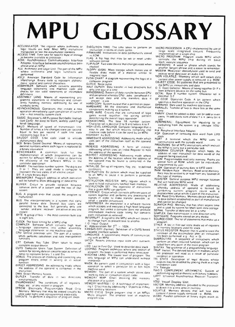
MPU GLOSSARY ACCUMULATOR 1 he register where arithmetic or
logic results are held Most MPU instructions manipulate or test the accumulator contents
ACCESS TIME Time take for specific byte of storage to become available to processor
ACIA: Asynchronous Communication Interface Adapter. Interface between asynchronous peri-pheral and an MPU
ALU Arithmetic and Logic Unit The part of the MPU where arithmetic and logic functions are performed
ASCII American Standard Code for Information Interchange Binary code to represent alphanu-meric special and control characters
ASSEMBLER Software which converts assembly language statements into machine code and checks for non valid statements or incomplete definitions
ASSEMBLY LANG Means of representing pro-gramme statements in mnemonics and conven-iently handling memory addressing oy use of symbolic terms
ASYNCHRONOUS Operations that initiate a new operation immediately upon completion of current one — not timed by system clock
BASIC: Beginner's All Purpose Symbolic Instruc-tion Code: An easy to learn, widely used high level language.
BAUD Measure of speed of transmission line Number of times a line changes state per second Equal to bits per second if each line state represents logic 0 or 1
BAUDOT CODE 5-bit code used to encode alphanumeric data
BCD Binary Coded Decimal Means of representing decimal numbers where each figure is replaced by a binary equivalent
BENCHMARK A common task for the implementation of which programmes can be written for different MPUs in order to determine the- efficiency of the different MPUs in the particular application
BINARY The two base number system The digits are 0 or 1 They are used inside a computer to represent the two states of an electric circuit
BIT A single binary digit BREAKPOINT Program address at which execution
will be halted to allow debugging or data entry
BUFFER Circuit to provide isolation between sensitive parts of a system and the rest of that system
BUG A program error that causel the program to malfunction
BUS The interconnections in a system that carry parallel binary data Several bus users are connected to the bus but generally only one sender and one receiver are active at any one
instant BYTE A group of bits the most common byte size
is eight bits
CLOCK The basic timing for a MPU Chip
COMPILER Software which converts high level . language statements into either assembly
language statements or into machine code CPU Central processor unit The part of a system
which performs calculation and data manipulation functions
CRT Cathode Ray Tube Often taken to mean complete output device
CUTS Computer Users Tape System Definition of system for storing data on cassette tape as series of tones to represent binary 1 s and 0 s
DEBUG The process of checking and correcting any program errors either in writing or in actual function
DIRECT ADDRESSING An addressing mode where the address of the operand is contained in the instruction
DMA Direct Memory Access DUPLEX Transfer of data in two directions
simultaneously ENVIRONMENT The conditions of all registers
flags etc at any instant in program EPROM Electrically Programmable Read Only
Memory Memory that may be erased lusually by ultra violet light) and reprogrammed electrically
EXECUTE To perform a sequence of program steps
EXECUTION TIME The time taken to perform an instruction in terms of clock cycles
FIRMWARE Instructions or data permanently stored in ROM
FLAG A flip flop that may be set or reset under software control
FLIP-FLOP Two state device that changes state when clocked
FLOPPY (DISK) Mass storage which makes use of flexible disks made of a material similar to magnetic tape
FLOW CHART A diagram representing the logic of a computer program
GLITCH Noise pulse HALF DUPLEX Data transfer in two directions but
only one way at a time HANDSHAKE: System of data transfer between CPU
and peripheral whereby CPU asks peripheral if it will accept data and only transfers data if answer is yes
HARD COPY System output that is printed on paper HARDWARE All the electronic and mechanical
components making up a system HARD WIRE Circuits that are comprised of logic
gates wired together the wiring pattern determining the overall logic operation
HEXADECIMAL The base 16 number system Character set is decimal 0 to 9 and letters A to F
HIGH LEVEL LANGUAGE Computer language that is easy to use but which requ.res compiling into machine code before it can be used by an MPU
HIGHWAY As BUS
IMMEDIATE ADDRESSING Addressing mode which uses part of the instruction itself as the operand data
INDEXED ADDRESSING A form of indirect addressing which uses an Index Register to hold the address of the operand
INDIRECT ADDRESSING Addressing mode where the address of the location where the address of the operand may be found is contained in the instruction
INITIALISE Set up all reg sters flag etc to defined conditions
INSTRUCTION Bit pattern which must be supplied to an MPU to cause it to perform a particular function
INSTRUCTION REGISTER MPU register which is used to hold instructions fetched from memory
INSTRUCTION SET The repertoire of instructions that a given MPU can perform
INTERFACE Circuit which connects different parts of system together and performs any processing of signals in order to make transfer possible œ serial — parallel conversion)
INTERPRETER An interpreter is a software routine which accepts and executes a high level language program but unlike a compiler does not produce intermediate machine code listing but converts each instruction as received
INTERRUPT A signal to the MPU which will cause it to change from its present task to another
I 0 Input Output K: Abbreviation for 21° = 1024. KANSAS CITY (Format) Definition of a CUTS based
cassette interface system LANGUAGE A systemmatic means of communicat-
ing with an MPU LATCH Retains previous input state until overwrit-
ten
LIFO Last In First Out Used to describe data stack LOOPING Program technique where one section of
program the loop) is performed many times over MACHINE LANG The lowest level of program The
only language an MPU can understand without interpreter
MASK Bit pattern used in coniunction with a logic operation to select a particular bit or bits from machine word
MEMORY The part of a system which stores data working data or instruction obiect code)
MEMORY MAP Chart showing the memory allocation of a system
MEMORY MAPPED I 0 A technique of implement-ing I 0 facilities by addressing I 0 ports as if they were memory locations
MICRO CYCLE Single program step in an MPUs Micro program The smallest level of machine program step
MICRO PROCESSOR A CPU implemented by use of large scale integrated circuits Frequently implemented on a single chip
MICRO PROGRAM Program inside MPU which controls the MPU chip during its basic fetch execute sequence
MNEMONIC A word or phrase which stands for another longer) phrase and is easier to remember
MODEM Modulator demodulator used to send and receive serial data over an audio link
NON VOLATILE: Memory which will retain data content after power supply is removed e g ROM
OBJECT CODE: Bit patterns that are presented to the MPU as instructions and data
O C Open Collector Means of tieing together 0 ,P s from different devices on the same bus
OCTAL Base 8 number system Character set is decimal 0-7.
OP CODE Operation Code A bit pattern which specifies a machine operation in the CPU
OPERAND Data used by machine operations PARALLEL Transfer of two or more bits at the same
time PARITY Check bit added to data can be odd or even
parity In odd parity sum of data 1 s + parity bit is odd
PERIPHERAL: Equipment for inputing to or outPutting from the system •e g teletype VDU etc
PIA Peripheral Interface Adapter POP Operation of removing data word from LIFO
posRtaick A terminal which the MPU uses to
communicate with the outside world PROGRAMS Set of MPU instructions which instruct
the MPU t 3 carry out a particular task PROGRAM COUNTER Register which holds the
address of next instruction (or data word) of the program being executed
PROM Programmable read only memory Proms are special form of ROM which can be individually programmed by user
PUSH Operation of putting data to LIFO stack RAM Random Acce Memory Read write memory
Data may be written to or read from any location in this type of memory
REGISTER General purpose MPU storage location that will hold one MPU word
RELATIVE ADDRESSING Mode of addressing
whereby address of operand is formed by combining current program count with a displacement value which is part of the instruction
ROM Read Only Memory Memory device which has its data content established as pert of manufacture and cannot be changed
SCRATCH PAD Memory that has short access time and is used by system for Short term data storage
SERIAL Transfer of data one bit at a time SIMPLEX Data transmission in one direction only SOFTWARE Programs stored on any media SOURCE CODE The list of statements that make up a
program
STACK A last in first out store made up of registers or memory locations used for stack
STATUS REGISTER Register that is used to store the condition of the accumulator after an instruction has been performed e g Acc 01
SUBROUTINE A sequence of instructions which perform an often required function which can be called from any point in the main program
SYNTAX The grammar of a programming language TRAP Vector) Pre-defined location in memory which
the processor will read as a result of particular condition or operation
TRI STATE Description of logic devices whose outputs may be disabled by placing them in a high impedance state
TTY Teletype
TWOS COMPLEMENT ARITHMETIC System of performing signed arithmetic with binary numbers
LJART Universal Asynchronous Receiver Transmit-ter
VDU: Visual Display Unit.
VECTOR Memory address provided to the processor to direct it to a new area in memory
VOLATILE Memory devices that will lose data content if power supply removed i e RAM)
WORD Parallel collection of binary digits much as byte