electronics and electromagnetics · pdf fileelectronics and electromagnetics ... early...
TRANSCRIPT


156 2010 NRL REVIEW
ELECTRONICS AND ELECTROMAGNETICS
Improvements to Towed Decoys to Enhance Aircraft Survivability
G.T. RoanTactical Electronic Warfare Division
Introduction: The towed decoy, which was developed by the Naval Research Laboratory in the early 1980s, has proven itself to be an effective coun-termeasure to radar-guided antiaircraft weaponry. The first-generation towed decoys repeat the radar signal electronically using a transmitter physically separated in angle from the defending aircraft. The repeater decoy then acts as a beacon for the radar to divert the weapon away from the aircraft. Figure 1 shows a
photograph of the NRL prototype, the Multi-Service Decoy, which was struck by an air-to-air missile in an early live-fire test. This proof of principle led to the production of the AN/ALE-50 Advanced Airborne Expendable Decoy that is currently operational on Air Force F-16 and B-1 and Navy F/A-18 aircraft. A second-generation towed decoy will soon become operational on the Navy’s F/A-18 E/F Super Hornet: the AN/ALE-55 Fiber Optic Towed Decoy (FOTD) of the Integrated Defensive Electronic Countermeasures (IDECM) System. With an FOTD, a more complex electronic countermeasures waveform can be gener-ated onboard the aircraft and communicated to the decoy through the towline. Unfortunately, both towed decoys have been beset with problems on the Super
Figure 1Multi-Service Decoy used in early live-fire tests.
Direct hit in live-fire tests against air-to-air missile

2010 NRL REVIEW 157
ELECTRONICS AND ELECTROMAGNETICS
Hornet because during combat maneuvers, the towline is exposed to hot engine exhaust gases that can far exceed 500 °C. The hot gases lead either to mechanical failure of the towline or optical fiber or to electrical failure of the wiring in the towline in some portions of the aircraft’s flight envelope. As a result, availability of the decoy is significantly limited while the aircraft is maneuvering. NRL's Tactical Electronic Warfare Division (TEWD), working with the Chemistry and the Materials Science and Technology Divisions and with industry, has developed a range of improvements to the towline components, the launcher, and the decoy itself to enhance decoy survivability and therefore aircraft survivability during combat operations.
Recent Research and Development: A decoy towline that includes an optical fiber is shown notionally in Fig. 2. Polyimide is normally used as wire insulation because of the requirements for high dielectric strength and for sufficient flexibility to pass a minimum bend radius of 6 mm. NRL researchers have focused on two materials with improved capability to function in the exhaust plume: a thermo-oxidatively stable polymer known as poly(carborane-siloxane-acetylene), or PCSA,1 and silica microtubing. A 12 μm coating of PCSA over a 75 μm coating of poly-imide raised the functional temperature of a pair of polyimide wires from 500 °C to 630 °C with a 5000 V potential difference, with little or no reduction in flexibility. PCSA was developed by NRL and is manu-factured by Triton Systems Incorporated under NRL direction. Higher temperatures of operation have been achieved using small-diameter (~350 μm) silica tubing with a wire in the center that is quite flexible (less than 6 mm bend radius) and yet capable of carrying electri-cal current at 5000 V at temperatures of up to 1000 °C.
Unfortunately, the silica-insulated wire has been too brittle to be used in the current towline, but modifica-tions to the launcher under consideration may enable its use in the near future. The silica-insulated wire is manufactured by Polymicro under an NRL patent.2
Researchers at both NRL and Meggitt Defense Systems are working to improve the tensile strength of the towline in the exhaust plume. In the current towline, Zylon, also known as PBO, provides adequate tensile strength at low temperature but it loses 50% tensile strength at 500 °C, and it weakens in the pres-ence of water vapor and in sunlight. NRL is experi-menting with towlines made using carbon fibers that have a higher tensile strength than Zylon at room temperature, and in a flame test at 1200 °C, a carbon fiber towline under 400 N of tension survives for 37 s as opposed to 2 s for Zylon. Unfortunately, carbon fibers burn in air, and a means to slow the combustion rate remains under investigation. Alternatively, Meggitt has constructed a hybrid towline using a noncom-bustible ceramic fiber called Nextel. Nextel is weaker than either Zylon or carbon fiber at room temperature, but a hybrid Nextel/Zylon towline maintains a tensile strength of 445 N at a temperature of 650 °C where Zylon decomposes. Two test flights have been carried out on an F/A-18 E/F using the hybrid Nextel/Zylon towline with promising results.
NRL and Meggitt Defense Systems are develop-ing modifications to the decoy launcher to reduce the stress applied to the towline. The F/A-18 E/F decoy launcher has a capacity for three single-use (expend-able) decoy canisters, each containing a decoy, several hundred feet of towline, and the spool and brake assembly within a volume of 7 cm by 7 cm by 48 cm. In the standard launcher, the decoy is ejected at a veloc-ity of 9 m/s using an explosive charge called a squib and the decoy is severed (not recovered) at the end of a mission. This explosive deployment places a high load on the towline at launch. Meggitt has developed a new magazine that slides into the existing launcher on the Super Hornet and ejects the decoy at a lower velocity (~5 m/s) using a spring. Once ejected from the launcher, the decoy is accelerated by the airstream drag as the towline spools from a free spinning reel assembly. Due to the low friction of the free spin-ning reel and the high acceleration of the decoy and towline by airstream drag, the decoy is fully deployed in less time than the standard launch using a squib, and with reduced strain on the towline. The strain on the towline is further reduced through a change to the AN/ALE-55 decoy fin assembly. The new magazine is also capable of recovering the decoy after a mission, potentially saving the Navy millions of dollars through reuse of decoys.
Zylon Jacket High Voltage Insulation
#34 Copper Wire
Buffered Optic Fiber
Figure 2Notional towline for a fiber optic towed decoy.

158 2010 NRL REVIEW
ELECTRONICS AND ELECTROMAGNETICS
Future Navy decoys will benefit from ongoing research into wide bandgap semiconductors (WBGS) such as silicon carbide (SiC) and gallium nitride (GaN). Current towed decoys, the AN/ALE-50 and AN/ALE-55, use a vacuum tube known as a travel-ing wave tube (TWT) to supply the RF power over a wide frequency range. Under a WBGS program sponsored by the Office of Naval Research (ONR) and the Defense Advanced Research Projects Agency (DARPA), microwave monolithic integrated circuit (MMIC) devices are being produced for use in solid-state power amplifiers that can now compete with the TWT in power and bandwidth. The MMIC operate at voltages between 20 and 50 V as compared to 2000 to 5000 V for a TWT, which is advantageous because a low-voltage towline is much less expensive to build than a towline carrying several thousand volts. Potentially, a solid-state RF power amplifier would cost thousands of dollars less than the TWT equivalent due to the economy of large-scale integrated circuit manufacturing.
In a demonstration project, NRL TEWD teamed with Cree, Inc., and Keragis Corporation to build a
prototype of a solid-state decoy using GaN MMIC. Cree3 developed the high-power GaN MMIC on a GaN/SiC substrate that measures 4 mm by 3 mm by 0.05 mm. Six of the MMIC devices were inserted into a novel, 5-cm-diameter cylindrical power combiner, built by Keragis, which provides an excellent thermal path to the airstream for dissipation of the heat gener-ated by the power MMIC. Figure 3 shows the solid-state towed decoy with the two power combiners.
Summary: NRL research led to the development of the towed decoy for the self-protection of Navy and Air Force aircraft from modern radar-guided weapons. Recent multidisciplinary research and development is adding to the operational capabilities of the towed decoy with new towlines capable of operating in a high-temperature exhaust plume, improved methods of deployment and recovery, and solid-state decoys with better reliability and lower lifecycle cost.
Acknowledgments: The author gratefully acknowledges the support of this work by the Office of Naval Research under Program Element 0603123N.
Figure 3Solid state towed decoy prototype with a pair of GaN solid state amplifiers.
FRONT COVER
TOW CABLE
PHOTO RECEIVER
TAIL ASSM
PHOTO RECEIVER MOUNTING PLATE
PRE AMPLIFIERMODULE ASSEMBLY
POWER SUPPLY SECTION
FRONT SECTION
PR / PRE AMP INTERFACEGPO CONNECTOR
RANDOMNONMETAL MATERIAL
PRE AMP / POWER AMP INTERFACEGPO CONNECTOR / SMA
ANTENNA/PA INTERFACESMA FEMALE / MALE
Power Amp Modules

2010 NRL REVIEW 159
ELECTRONICS AND ELECTROMAGNETICS
The author also acknowledges the contributions of NRL coresearchers Teddy Keller and Manoj Kolel-Veetil of the Chemistry Division, and Ron Tonucci and Harry Jones of the Materials Science and Technology Division.
[Sponsored by ONR]
References1 M.K. Kolel-Veetil and T.M. Keller, “Polymeric Protection of
Navy Fighter Jet Towlines,” 2007 NRL Review, pp. 147–148 (2008).
2 R.J. Tonucci and G. Roan, “High Voltage High Temperature Wire,” United States Patent 7,002,072, Feb. 21, 2006.
3 J.W. Milligan, S. Sheppard, W. Pribble, A. Ward, and S. Wood, “SiC and GaN Wide Bandgap Technology Commercial Status,” International Conference on Compound Semiconductor Manufacturing Technology, April 14–17, 2008, Chicago, IL.
Adaptive Jamming Cancellation in Radar
V. Gregers-Hansen, R. Mital, and J. CookRadar Division
Introduction: The new core mission for the Navy is integrated air and missile defense (IAMD). This combines conventional anti-air warfare (AAW) against aircraft and missiles, with ballistic missile defense (BMD) against short- and medium-range ballistic missile threats to Navy sea-based assets or high-value land-based targets. New radars designed to support this mission must meet difficult requirements for very long range detection and discrimination of lethal objects, and provide high-precision weapons control. All of these requirements must be achieved while incurring little to no degradation in performance in the presence of anticipated intense electronic attack (EA) while operating in an environment of heavy clutter and interference. While the entire gamut of EA techniques must be considered in the radar design, the specific threat of high-power barrage noise jamming
from long-range standoff jammers is of particular concern.
Traditional radar approaches dealing with the standoff jamming threat consist of a combination of low antenna sidelobes and adaptive nulling techniques. Because in many cases low antenna sidelobes alone cannot mitigate standoff jammers, adaptive jamming cancellation systems are added to the radar to reduce jamming residues to an acceptable level.1 Adaptive jamming cancellation systems have often failed to meet expectations due to a lack of understanding of factors such as system bandwidth, multipath reflec-tions, number of simultaneous jammers, and hardware tolerances and inefficiencies. A research project in the Radar Division is seeking to improve the understand-ing of these limitations through a high-fidelity model-ing and simulation effort. This article gives a brief overview of sidelobe canceller implementations, pres-ents the development of a suitable simulation model, and provides performance predictions for a specific sidelobe canceller design.
Jamming Scenario Assumed: A typical jamming scenario confronted by a Navy radar is illustrated in Fig. 4. The scenario includes a number of simultaneous jamming platforms (NJ = 4 shown), each at range R J and with an effective radiated power density (ERPD) defined in units of dBW/MHz. It is assumed that the combination of jammer ERPD and its standoff range results in a jamming-to-noise ratio (JNR) in an isotropic sidelobe of JNR = 30 dB. The jammers are distributed over an angular threat sector (±30° shown in Fig. 4) and at specified elevation angles. If any of the jammers enters the main beam region, supplementary main beam cancellation techniques would be required but this aspect of performance is not addressed here. In a typical at-sea environment, the jamming signals can enter the radar antennas via direct and indirect paths. The indirect path is the “multipath” signal defined by its relative amplitude and time delay as it enters the radar antennas.
Main Beam Direct Pathand Multipath
Figure 4Notional jamming environment; jammers are randomly located across the ±30° angular sector but outside the main beam.

160 2010 NRL REVIEW
ELECTRONICS AND ELECTROMAGNETICS
Dispersion of the received jamming across the spatial extent of the main and auxiliary antennas becomes a limiting factor on performance when jamming suppression over a wide bandwidth is required. The effect of dispersion is greatest for jammers furthest away from array boresight.
Sidelobe Canceller (SLC) Simulation: The objec-tive of an SLC system is to suppress jamming received through the sidelobes of a radar antenna. Using a number of additional antenna elements, usually desig-nated as the auxiliary (AUX) antennas, it is possible to place nulls in the directions of the interfering signals by subtracting weighted versions of the signal received in the AUX antennas. A simple block diagram of a sidelobe cancellation system is shown in Fig. 5. For the simulation results presented in the next section, a main antenna array with a 4 m diameter (D = 4 m) is assumed. This figure shows NA
= 4 AUX anten-nas placed along the perimeter of the main array at locations that are selected randomly within each of four quadrants. For practical reasons, no auxiliary antennas are usually located inside the main array. The maximum number of nulls that can be placed in the direction of jammers is equal to the number of AUX antennas. Also shown in Fig. 5 is the use of “fast taps” at the output of each AUX antenna spaced in time by Δ seconds. These fast taps (L = 3) do not
allow the sidelobe canceller to suppress additional jammers, but they can improve cancellation perfor-mance, particularly against wide bandwidth jamming and multipath. Thus, a total of NA ⋅ L channels weighted by an identical number of complex weights ( �w w w wN LA
= ( )( )⋅1 2, ,... ) are used to suppress the jamming received in the main channel. The computa-tion of these adaptive weights is based on a number NS of complex samples collected simultaneously from the main and AUX channel using a suitable algorithm. For the results presented here, use of the near optimal sample matrix inversion technique is assumed.
In the sidelobe canceller simulation, all channels are bandpass filtered in Gaussian filters of bandwidth B. The jamming entering the radar antennas has a rectangular bandwidth of width 4 ⋅ B and is sampled at its respective Nyquist rate. This complex-sampling rate of 4 ⋅ B is maintained through the signal processor. The simulation of the sidelobe canceller system shown in Fig. 5 takes into account all group and phase delays based on jammer angular locations and antenna phase centers. While the phase centers of the AUX antennas are accurately characterized by their physical location, the phase center of the main antenna in the sidelobe region is a random variable determined by the specific sidelobe characteristics in the jammer direction. In the simulation, a horizontal linear array of elements is used to represent the actual circular array in the
Time (s)
Figure 5Simplified sidelobe canceller block diagram.

2010 NRL REVIEW 161
ELECTRONICS AND ELECTROMAGNETICS
simulation. This approximation is valid since the jammers are all at almost the same elevation angle but widely distributed in azimuth. Using this simplifica-tion, the array can be represented by a linear array of NEL = 88 elements rather than about 6000 as needed to populate a 4 m diameter array at S-band. The linear array is weighted by a 50 dB Taylor function, and random amplitude and phase errors are added at each element to result in a median sidelobe level of around -10 dBi. The AUX antenna gain is assumed to be GAUX = 8 dB. Both main antenna sidelobes and the AUX gain pattern are modulated by the same element pattern. With this representation of the main antenna, its impulse response from any jammer directions is simply given by the element weights with a time-tap spacing given by the projection of the element spacing on the jammer direction. From this tapped delay line representation, the frequency response of the array to the jamming can be calculated using the chirp-transform technique. The operation of the coherent
sidelobe canceller is illustrated in Fig. 6, showing the effective sidelobe pattern of the main antenna in the presence of four jammers before and after jamming cancellation.
Simulation Results: The performance results assume a scenario with four standoff jammers as previously described. It is desired to design a sidelobe cancellation system that will suppress jamming over a B = 50 MHz bandwith such that the jamming-plus-thermal noise to thermal noise ratio is less than 5
dB with a 90% probability. Figure 7 shows four key performance trade-offs leading to such a design. In Fig. 7(a), the number of auxiliary antennas is varied between two and eight for a relatively narrow band-width of B = 1 MHz. With only NA = 2 or 3 AUX antennas, performance is poor because the system has insufficient degrees of freedom to create nulls in four directions simultaneously. For NA = 4, performance is much improved but ill conditioning results in occa-sional larger residues. Therefore, the number of AUX antennas for our design example was chosen as NA = 6.
Figure 7(b) shows the effect of increasing the system bandwidth beyond the 1 MHz value assumed for Fig. 7(a). It can be seen that for a 50 MHz band-width, performance is significantly worse than the requirement due to time-delay and dispersion effects.
In Fig. 7(c), fast time taps have been added to the basic sidelobe canceller, as shown in Fig. 5. The tap spacing was 2 ns (~0.1/B), and the number of equidis-tant taps was varied from one to four. It can be seen
that L = 3 results in a sidelobe canceller design meeting the requirement.
Finally, Fig. 7(d) shows the effect of the number of samples from each channel used to cal-culate the weights. All previous results used a large number of samples (NS = 8092) to approxi-mate optimum performance. In Fig. 7(d), the number of samples was reduced to as few as 64. To avoid significant performance degradation due to inadequate sample support, use of at least NS = 128 samples is required.
Conclusion: A modeling and simulation effort to predict the performance of a sidelobe canceller has been described. As an example of the use of this model, a sidelobe cancel-ler design for suppression of
jamming from NJ = 4 independent jamming sources with a system bandwidth of 50 MHz to a residue level of less than 5 dB above thermal noise with a 90% prob-ability was considered. The resulting design requires four AUX antennas, three fast taps per channel spaced by 2 ns, and at least 128 training samples per channel.
Other features of the simulation model developed under this project include the modeling of multipath effects from the sea surface, also known as “hot clutter,” and main beam jamming cancellation using high-gain AUX antennas. A complete description
Figure 6Illustration of nulling of four jammers by adaptive sidelobe cancellation (SLC).
Post-Adapted Main Beam PatternJammerPre-Adapted Main Beam Pattern
Ant
enna
Gai
n (d
B)
Azimuth (degrees)
40
20
0
-20
-40
-60
-80
-100-90 -70 -50 -30 -10 10 30 50 70 90

162 2010 NRL REVIEW
ELECTRONICS AND ELECTROMAGNETICS
Figure 7(a)Effect of number of auxiliary antennas on SLC perfor-mance for NJ = 4 jammers and bandwidth B = 1 MHz.
Figure 7(b)Effect of radar bandwidth on SLC performance for a fixed number of jammers and auxiliary antennas (NJ = 4 and NA = 6).
Figure 7(d)Effect of number of training samples on SLC perfor-mance for NJ = 4, NA = 6, 3 fast taps with 2-ns spacing, and a 50 MHz bandwidth.
Figure 7(c)Effect of the number of fast taps with 2-ns spacing on SLC performance for NJ = 4 jammers, NA = 6 auxiliary antennas, and a B = 50 MHz system bandwidth.
of this work will be included in a forthcoming NRL Report.
[Sponsored by NRL]
Reference1 R.A. Monzingo and T.W. Miller, Introduction to Adaptive Arrays
(John Wiley & Sons, New York, NY, 1980).
Laser System for Protection of Navy Ships
P. Mak and C. MaravigliaTactical Electronic Warfare Division
Introduction: Antiship missiles (ASM) are an acknowledged threat to U.S. Navy ships. Many of these missiles are TV-guided, infrared-guided, or have an operator-in-the-loop in the terminal phase of their engagement. Improved ship survivability against these optically guided and imaging threats requires the development of a laser-based, multiband countermea-sure (CM) capability that will also enable an onboard/offboard response against advanced threats if neces-sary. We describe here the development, fabrication, and testing of a laser-based, smart jamming electro-optic/infrared (EO/IR) CM system called SHIELDS
(Shipboard Integrated Electro-optic Defense System), which is designed to counter currently deployed and emerging ASM threats.
System Description: NRL’s research on laser-based IRCM for ship defense since the late 1980s had generated a set of EO/IR CM requirements based upon which Lockheed Martin developed and fabricated SHIELDS. SHIELDS was designed to perform the fol-lowing functions when engaging an ASM: acquire the missile threat after a target handoff from a radar or an IR search and track system; track the target; turn the lasers on for active tracking and target interrogation; perform smart jamming; and evaluate CM effective-ness. SHIELDS comprises the following subsystems: a multifunction IR camera, a high-frame-rate visible camera, a multiband IR/visible laser system (MIRVLS), a stabilized optical pointer, an optical assembly/turret, and a universal processor (UP). Most of these com-ponents are form and function compatible with the shipboard version to ease technology transition.
The IR camera has a narrow field of view (FOV) and a high-resolution focal plane array (FPA) for target detection and tracking. It is also used for active detection/tracking and target interrogation when engaging an in-band threat. The high sensitivity and

2010 NRL REVIEW 163
ELECTRONICS AND ELECTROMAGNETICS
resolution of the camera provide a shipboard capabil-ity to evaluate the effectiveness of soft-kill or hard-kill CM by monitoring the target’s response to the CM. The camera has a variable frame rate to meet various per-formance requirements. The TV camera has the same FOV and a high-resolution detector FPA. It performs the same functions as the IR camera.
The key components of MIRVLS, developed by BAE Systems, are a thulium fiber laser, a holmium-doped YAG laser, and two wavelength converters. The fiber laser pumps the YAG laser, which sequentially pumps an IR wavelength converter and a visible wave-length converter to generate IR and visible outputs, respectively. The pulsed laser is comprised of three modules: a shoe box sized optical head, the fiber laser, and an electronic control unit. The laser output waveform is controlled by the pump diodes in the fiber laser. The laser functions are active target tracking, target interrogation, and jamming.
The field of regard of the EO/IR sensors and laser beam steering are controlled by a stabilized optical pointer (SOP). The SOP has a gimbaled mirror assembly (GMA) that can rotate to any posi-tion within 360° in 0.6 s. With this agile component, SHIELDS will be capable of engaging multiple targets rapidly. The SOP will provide horizontal coverage against sea-skimming threats and is stabilized for a surface combatant up to sea state 5.
To minimize the SOP size and the complexity of the SHIELDS optical train, all of the transceiver and
optical components are integrated into a common optical path. This common path includes the exter-nal window, SOP pointing mirror, MIRVLS, EO/IR cameras, and beam-combining elements. All alignment-critical components are mounted rigidly to an optical bench, which is supported at four corners by shock/vibration isolators. The optical assembly and the SOP are installed inside a turret as shown in Fig. 8. The Rotating Environmental Hood (REH) is slaved to the SOP/GMA azimuth position and provides mechanical isolation from external forces (such as wind load and hood friction).
The functions of the UP are threat management, acquisition, tracking, SOP motion control, EO/IR closed-loop CM, system control, and interfaces to other SHIELDS subsystems. The UP has six VME boards. Core SHIELDS processing is performed by a two-board commercial-off-the-shelf module (for motion control) and two custom boards that combine the strengths of the PowerPC with an array of very high-density field programmable gate arrays to perform SHIELDS track processing and countermea-sure functions.
All of the aforementioned subsystems, com-ponents, a host computer, data acquisition system, mass data storage, and associated power supplies and controls are installed in an 8-ft × 8-ft × 20-ft shelter as shown in Fig. 9, which also includes a SHIELDS system block diagram. The turret sits inside the shelter during system checkout, laser alignment or adjustment, and
Figure 8SHIELDS turret and its transceiver and optics components.

164 2010 NRL REVIEW
ELECTRONICS AND ELECTROMAGNETICS
Figure 9SHIELDS shelter and system block diagram.
Figure 10SHIELDS field trials at NRL/CBD.
SHieLDS Block Diagram
Shelter-based equipment
UniversalProcessor
Rack
HostProcessor
Rack
LaserControlRack

2010 NRL REVIEW 165
ELECTRONICS AND ELECTROMAGNETICS
system storage. The side door of the shelter allows the turret to be operated inside the shelter if needed. The turret was raised to the roof of the shelter during SHIELDS field trials.
Field Demonstrations: In 2009, NRL designed and conducted four phases of field trials, as illustrated in Fig. 10, at the NRL Chesapeake Bay Detachment (CBD) to evaluate the effectiveness of SHIELDS against ASM seekers. In the static-on-static (SS) phase, the SHIELDS shelter was moved to a concrete pad at NRL/CBD, about 120 ft above the bay, and the seekers were installed in a test tower 75 ft above the bay on Tilghman Island (TI) over 10 km away. In the static-on-dynamic (SD) phase, the static SHIELDS engaged a test asset that was captive-carried on a Learjet. In the dynamic-on-static (DS) phase, SHIELDS was installed on NRL’s Landing Craft, Mechanized (LCM), which was then maneuvered out to the Chesapeake Bay to test against the seekers mounted in the TI tower. These three sets of testing led to the dynamic-on-dynamic (DD) phase, which involved SHIELDS on a moving LCM and engaging captive-carried seekers flown on a Learjet.
NRL selected a wide array of test assets that repre-sent operational and future-generation optically guided ASM threat technologies for SHIELDS testing. The test assets included four IR- and two TV-guided seekers. Two of the IR seekers are FPA-based simulators devel-oped by NRL. The other two IR seekers are surrogates of threat systems. The visible band seekers are used in operational missile systems.
The result of the field trials was the first-ever dem-onstration of shipboard closed-loop IRCM (CLIRCM) and closed-loop EOCM (CLEOCM) capabilities against airborne ASM seekers from a maneuvering ship on water. Successful CLIRCM and CLEOCM tests conducted at tactically significant ranges against EO/IR ASM seekers included target handoff, acquisition, coarse and fine track, active target acquisition, active track, target interrogation and classification, optical breaklock, and lock transfer that simulated onboard/offboard IRCM.
Conclusion: NRL has developed and demon-strated laser-based EO/IR CM technology that is ready for shipboard transition. Required SHIELDS upgrades include component ruggedization for harsh shipboard environments and SHIELDS interface to combat systems.
[Sponsored by ONR]
Particle Filters for Multipath Mitigation
M. Hock and K. LeeTactical Electronic Warfare Division
Introduction: The Navy requires high-precision electronic support (ES) angle measurements so that closely spaced targets at the horizon can be separated, identified, and tracked. It is especially important to have high-precision angle estimates for cueing ship-board radars, for tracking emitters passively, and for correlating ES and radar reports. When the received signal is corrupted by multipath, conventional angle estimation algorithms can produce angle estimates that are many tens of degrees in error. In recent years, some new angle estimation algorithms such as modified sub-space methods and maximum likelihood techniques have been developed to address this problem. But these existing algorithms still have some limitations. The objective of this research is to improve the capability to track low-angle targets over the sea surface by develop-ing new elevation angle tracking algorithms based on particle filters. The multipath problem is highly non-linear and particle filters are a new approach suited to nonlinear problems.
Multipath Problem at Sea: Figure 11 illustrates the multipath problem at sea. The ES antenna on the ship receives two strong signals from the same target.1 One signal arrives along a direct path from the target and the second signal is reflected off the ocean surface. The direct and reflected signals have nearly the same magnitude when the sea surface is smooth and the target is at low elevation. The two signals are also coherent and there is severe interference between them. There is also a third component to the multipath signal, referred to as diffuse scattering, which is a sum of small reflections from the irregular sea surface.
We assume that measurements are obtained from an interferometer direction finding (DF) sensor in this research. Performance of the interferometer is seri-ously degraded by multipath.
State Space Model for Tracking Under Multipath: The core of the research involves reformu-lating existing models of multipath interference to fit them into the state-space framework of particle filters. The general form of the discrete-time state-space model is specified by the following state equation and measurement equation:
where xk is the state vector, zk is the measurement
x f x wk k k= ( )
− −1 1,
z h x vk k k= ( ),

166 2010 NRL REVIEW
ELECTRONICS AND ELECTROMAGNETICS
Figure 11Multipath over the sea surface.
Figure 12Particle representation of a probablity density function.
vector, wk is process noise, and vk is measurement noise. In the multipath problem, the function f is a kinematic model of target motion and the function h is a nonlinear deterministic model of the multipath interference. Several multipath models with different levels of detail are being formulated. The most appro-priate model for a particular application depends on the degree of information that is available concerning the position of the antenna array and sea state. When full information is available, the most detailed model can be applied.
Particle Filters: Particle filters2 are signal process-ing techniques that are used to estimate the state of nonlinear dynamic systems. They can be applied to any state-space model and are a generalization of the traditional Kalman filter used for linear systems. The key idea of the particle filter is to represent a complex probability density function by a set of samples (“par-ticles”) and associated weights. The concept is shown in Fig. 12, where the green line represents a complex density, black dots represent particles, and pink dots represent associated weights. A large number of par-ticles can provide a close approximation to the density.
The particles and weights are updated after each measurement is received and the estimate of the state is made based on the weighted particle set. A number of variants of the particle filter have been developed. In our research we have applied both sequential importance resampling (SIR) particle filters and cost-reference particle filters.3 Cost-reference particle filters have some advantages for implementation in that they do not require knowledge of the measurement noise distribution and can be designed with a structure suit-able for parallel processing.
Testing with Measured Data: Prerecorded field data are being used to evaluate the algorithms and to identify needed enhancements. The available data sets were collected from a scenario with an inbound low-elevation target approaching the sensor from various azimuth angles. Figure 13 shows a typical result com-paring true elevation and estimated elevation. The data set is processed by a conventional direction finding algorithm and the NRL particle filter. The conventional method does not provide accurate elevation angle estimates and it also generates outliers, denoted by the black x’s, that lie outside the viewing range of the graph. The particle filter generates more accurate and smoother estimates without any outliers.
Summary: Particle filters are being applied to improve the capability to track low-elevation targets over a smooth sea surface. The research involves developing state-space models for target elevation under multipath conditions and implementing particle filters. Because the particle filter incorporates both a kinematic model of target motion and a model of mul-tipath signal propagation, the particle filter algorithms demonstrate superior performance to the conventional method with real data.
[Sponsored by NRL and ONR]

2010 NRL REVIEW 167
ELECTRONICS AND ELECTROMAGNETICS
References1 L. Blake, Radar Range-Performance Analysis (Artech House,
Norwood, MA, 1986).2 B. Ristic, D. Arulampalam, and N. Gordon, Beyond the Kalman
Filter (Artech House, Boston, MA, 2004).3 J. Miguez, S. Xu, M. Bugallo, and P. Djuric, “Particle Filtering
for Systems with Unknown Noise Probability Distributions,” Proceedings of the 2003 IEEE Workshop on Statistical Signal Processing, St. Louis, MO, pp. 522–525, Sept. 2003.
A New Gallium Nitride–based Switch for High Efficiency Power Electronics
T.J. Anderson,1 M.J. Tadjer,2 M.A. Mastro,1 J.K. Hite,1 K.D. Hobart,1 C.R. Eddy, Jr.,1 and F.J. Kub1
1Electronics Science and Technology Division2University of Maryland
Introduction: A long-sought goal for gallium nitride (GaN)-based transistor research has been the development of a reliable, fast, efficient, normally-off power switch. Such a device would have a wide range of immediate military power converter applications, such as high-power satellite communications and radar, unmanned underwater vehicles, ship drive
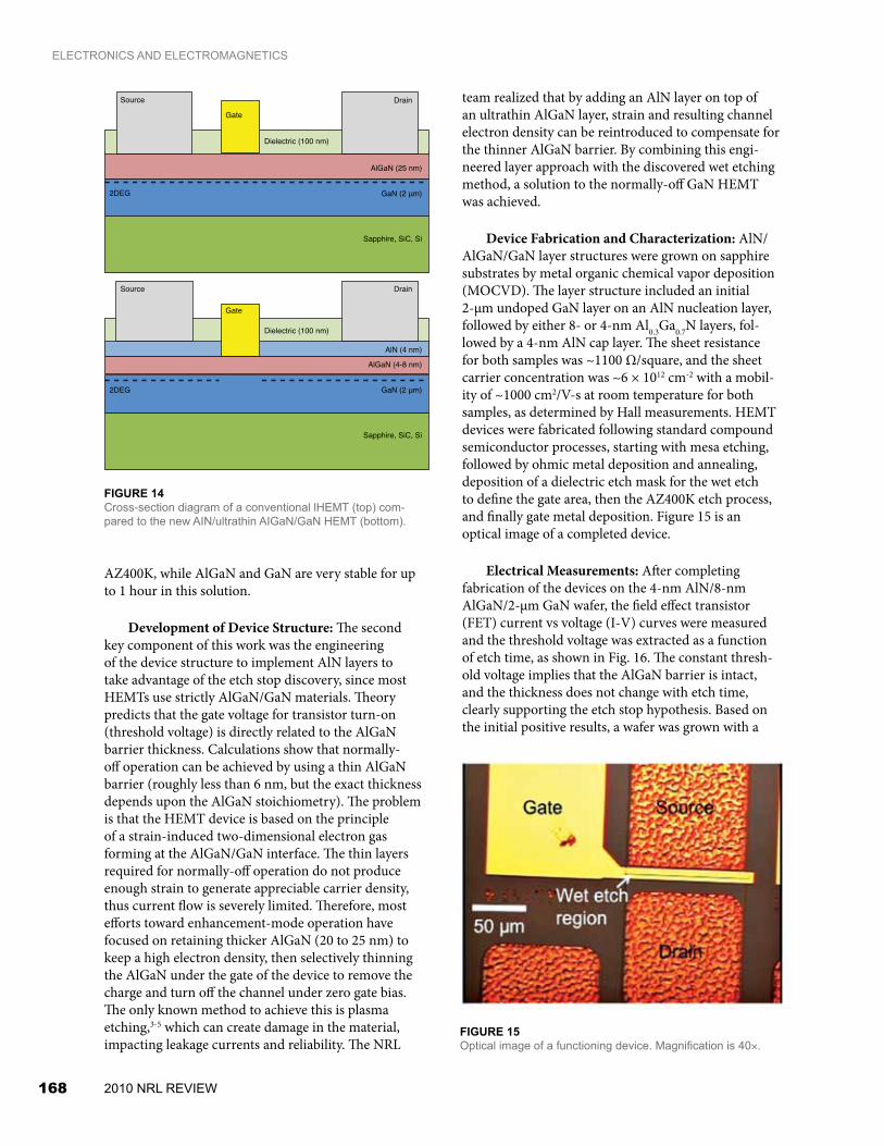
components, and hybrid vehicle inverters. As a wide bandgap semiconductor, GaN is attractive for its high mobility, high power capability, and chemical and thermal stability, but GaN transistors typically have normally-on (depletion mode) characteristics, which offer limited fail-safe properties. The NRL Power Electronics Branch has realized the first enhancement-mode aluminum gallium nitride (AlGaN)/GaN high electron mobility transistor (HEMT) fabricated by a selective wet etch approach,1 shown compared to a conventional depletion mode transistor in Fig. 14.
Development of a Selective Etch: The first key discovery was a chemically selective etch for aluminum nitride (AlN) over gallium-containing compounds such as AlGaN and GaN. Wet etching of AlN using heated AZ400K photoresist developer has been reported in the literature,2 but its effectiveness in etching AlGaN or GaN is not understood. AZ400K is a potassium borate based solution with a pH around 13, which is already commonly used in diluted form in virtually every step in semiconductor fabrication. We have verified, using scanning electron microscopy (SEM) and X-ray photoelectron spectroscopy (XPS), that AlN does in fact etch at a slow rate in near-boiling
Figure 13Elevation estimates from the conventional DF and the particle filter.
Elevation Angle Tracking
Ele
vatio
n (d
egre
es)
True ElevationConventional Direction FindingOutliers from Conventional DFParticle Filter
Time (seconds)0 20 40 60 80 100
1.5
1
0.5
0
-0.5
168 2010 NRL REVIEW
ELECTRONICS AND ELECTROMAGNETICS
AZ400K, while AlGaN and GaN are very stable for up to 1 hour in this solution.
Development of Device Structure: The second key component of this work was the engineering of the device structure to implement AlN layers to take advantage of the etch stop discovery, since most HEMTs use strictly AlGaN/GaN materials. Theory predicts that the gate voltage for transistor turn-on (threshold voltage) is directly related to the AlGaN barrier thickness. Calculations show that normally-off operation can be achieved by using a thin AlGaN barrier (roughly less than 6 nm, but the exact thickness depends upon the AlGaN stoichiometry). The problem is that the HEMT device is based on the principle of a strain-induced two-dimensional electron gas forming at the AlGaN/GaN interface. The thin layers required for normally-off operation do not produce enough strain to generate appreciable carrier density, thus current flow is severely limited. Therefore, most efforts toward enhancement-mode operation have focused on retaining thicker AlGaN (20 to 25 nm) to keep a high electron density, then selectively thinning the AlGaN under the gate of the device to remove the charge and turn off the channel under zero gate bias. The only known method to achieve this is plasma etching,3-5 which can create damage in the material, impacting leakage currents and reliability. The NRL
team realized that by adding an AlN layer on top of an ultrathin AlGaN layer, strain and resulting channel electron density can be reintroduced to compensate for the thinner AlGaN barrier. By combining this engi-neered layer approach with the discovered wet etching method, a solution to the normally-off GaN HEMT was achieved.
Device Fabrication and Characterization: AlN/AlGaN/GaN layer structures were grown on sapphire substrates by metal organic chemical vapor deposition (MOCVD). The layer structure included an initial 2-μm undoped GaN layer on an AlN nucleation layer, followed by either 8- or 4-nm Al0.3Ga0.7N layers, fol-lowed by a 4-nm AlN cap layer. The sheet resistance for both samples was ~1100 Ω/square, and the sheet carrier concentration was ~6 × 1012 cm-2 with a mobil-ity of ~1000 cm2/V-s at room temperature for both samples, as determined by Hall measurements. HEMT devices were fabricated following standard compound semiconductor processes, starting with mesa etching, followed by ohmic metal deposition and annealing, deposition of a dielectric etch mask for the wet etch to define the gate area, then the AZ400K etch process, and finally gate metal deposition. Figure 15 is an optical image of a completed device.
Electrical Measurements: After completing fabrication of the devices on the 4-nm AlN/8-nm AlGaN/2-μm GaN wafer, the field effect transistor (FET) current vs voltage (I-V) curves were measured and the threshold voltage was extracted as a function of etch time, as shown in Fig. 16. The constant thresh-old voltage implies that the AlGaN barrier is intact, and the thickness does not change with etch time, clearly supporting the etch stop hypothesis. Based on the initial positive results, a wafer was grown with a
Figure 15Optical image of a functioning device. Magnification is 40×.
Source
Source
Gate
Drain
Drain
Gate
Dielectric (100 nm)
Dielectric (100 nm)
2DEG
2DEG GaN (2 μm)
Sapphire, SiC, Si
AlGaN (4-8 nm)
GaN (2 μm)
Sapphire, SiC, Si
AlGaN (25 nm)
AlN (4 nm)
Figure 14Cross-section diagram of a conventional lHEMT (top) com-pared to the new AIN/ultrathin AIGaN/GaN HEMT (bottom).

2010 NRL REVIEW 169
ELECTRONICS AND ELECTROMAGNETICS
4-nm-thick AlGaN layer, which was expected to yield a positive threshold voltage based on fundamental cal-culations. Following the previously described standard fabrication process, a threshold voltage of +0.21 V was extracted from the FET I-V curves, as shown in Fig. 17. This value is consistent with reports of structures using comparable AlGaN thickness,6 and with theoreti-cal calculations based upon other measured device parameters.
Summary: NRL has achieved the first normally-off GaN HEMT fabricated through device structure engineering and a wet chemical recess etch of the gate region. The achievement employed a device structure incorporating an AlGaN/GaN HEMT with an ultra-thin AlGaN layer for positive threshold voltage, capped with a thin AlN layer to increase channel charge. Subsequently, a selective wet chemical etch was used to open the AlN layer and stop cleanly on the AlGaN surface, resulting in a normally-off device. The selec-tive wet etch approach improves manufacturability since etch stop layers can be built in to the device structure. This will improve reliability and process control, which represents a significant development toward commercialization of GaN power switches.
Acknowledgments: The authors are sincerely grateful to the microwave HEMT device group at NRL (S. Binari et al.) for insightful discussions and equipment use, the NRL Institute for Nanoscience for equipment use and support, and G. Jernigan of the Electronics Science and Technology Division for XPS characterization. JKH acknowledges the support of the American Society for Engineering Education/Naval Research Laboratory Postdoctoral Fellowship Program.
[Sponsored by ONR]
References1 T.J. Anderson, M.J. Tadjer, M.A. Mastro, J.K. Hite, K.D. Hobart,
C.R. Eddy, Jr., and F.J. Kub, “An AlN/Ultrathin AlGaN/GaN HEMT Structure for Enhancement-Mode Operation Using Selective Etching,” IEEE Electron Device Lett. 30(12), 1251–1253 (2009).
2 S.J. Pearton, J.C. Zolper, R.J. Shul, and F. Ren, “Processing Defects and Devices,” J. Appl. Phys. 86(1), 1–78 (1999).
3 W. Saito, Y. Takada, M. Kuraguchi, K. Tsuda, and I. Omura, “Recessed-gate Structure Approach toward Normally-off High Voltage AlGaN/GaN HEMT for Power Electronics Applications,” IEEE Trans. Electron. Devices 53(2), 1–7 (2006).
4 M. Kuraguchi, Y. Takada, T. Suzuki, M. Hirose, K. Tsuda, W. Saito, Y. Saito, and I. Omura, “Normally-off GaN MISFET with Well-controlled Threshold Voltage,” Phys. Status Solidi A 204(6), 2010–2013 (2007).
5 S. Maroldt, C. Haupt, W. Pletschen, S. Müller, R. Quay, O. Ambacher, C. Schippel, and F. Schwierz, “Gate-recessed AlGaN/GaN Based Enhancement-mode High Electron Mobility Transistors for High Frequency Operation,” Jap. J. Appl. Phys. 48(4), 04C083/1–04C083/3 (2009).
6 Y. Ohmaki, M. Tanimoto, S. Akamatsu, and T. Mukai, “Enhancement-mode AlGaN/AlN/GaN High Electron Mobility Transistor with Low On-state Resistance and High Breakdown Voltage,” Jap. J. Appl. Phys. 45(44), L1168–L1170 (2006).
Figure 16Threshold voltage (VT) and on-resistance as a function of etch time.
Figure 17VGS-IDS curve for 4-nm AlN/4-nm AlGaN/2-μm GaN structure. The drain bias was 5 V, and extracted VT was +0.21 V. The VDS-IDS curve is shown in the inset.
0 10 20 30 40 50
Etch Time (min)
V T (V)
-0.4
-0.5
-0.6
-0.7
-0.8
-0.9
-1
-1.1
-1.2
106
105
104
1000
100
RO
N (Ω-m
m)
-4 -3 -2 -1 0 1 2 3
VG (V)
0.05
0.04
0.03
0.02
0.01
0
0 1 2 3 4 5
I DS (
A/m
m)
VDS (V)
Vg = 2 VVstep = -0.5 V
0.03
0.025
0.02
0.015
0.01
0.005
0
I DS (
A/m
m)