electronic supplementary information engineering ... · pdf fileelectronic supplementary...
TRANSCRIPT

Electronic Supplementary Information
Engineering dielectric constants in organic semiconductors
Ardalan Armin, Dani M. Stoltzfus, Jenny E. Donaghey, Andrew J. Clulow, Ravi Chandra Raju
Nagiri, Paul L. Burn,* Ian R. Gentle, Paul Meredith#
aCentre for Organic Photonics & Electronics, School of Chemistry and Molecular Biosciences and
School of Mathematics and Physics, The University of Queensland, St Lucia Campus, Brisbane
4072 (Australia)# Now at: Department of Physics, Swansea University, Singleton Park, Swansea SA2 8PP, Wales, United Kingdom
*Email: [email protected]; [email protected]
Contents
1. Effect of excess energy on the internal quantum efficiency
2. NMR spectra of final compounds
3. Differential scanning calorimetry (DSC)
4. Photoluminescence spectra
5. Optical gap and extinction coefficients
6. X-ray analysis
7. Cyclic voltammetry (CV)
8. Mobility data
9. Homojunction OPV data
Electronic Supplementary Material (ESI) for Journal of Materials Chemistry C.This journal is © The Royal Society of Chemistry 2017
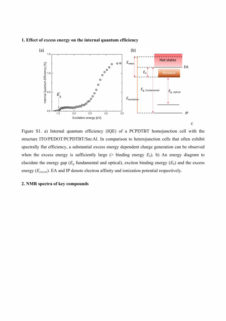
1. Effect of excess energy on the internal quantum efficiency
c
Figure S1. a) Internal quantum efficiency (IQE) of a PCPDTBT homojunction cell with the
structure ITO/PEDOT/PCPDTBT/Sm:Al. In comparison to heterojunction cells that often exhibit
spectrally flat efficiency, a substantial excess energy dependent charge generation can be observed
when the excess energy is sufficiently large (> binding energy Eb). b) An energy diagram to
elucidate the energy gap (Eg fundamental and optical), exciton binding energy (Eb) and the excess
energy (Eexcess). EA and IP denote electron affinity and ionization potential respectively.
2. NMR spectra of key compounds

Figure S2. 1H NMR spectrum of 4
Figure S3. 13C NMR spectrum of 4

Figure S4. 1H NMR spectrum of 2a

Figure S5. 13C NMR spectrum of 2a
Figure S6. 1H NMR spectrum of 3a

. Figure S7. 13C NMR spectrum of 3a

Figure S8. 1H NMR spectrum of DG
Figure S9. 13C NMR spectrum of DG
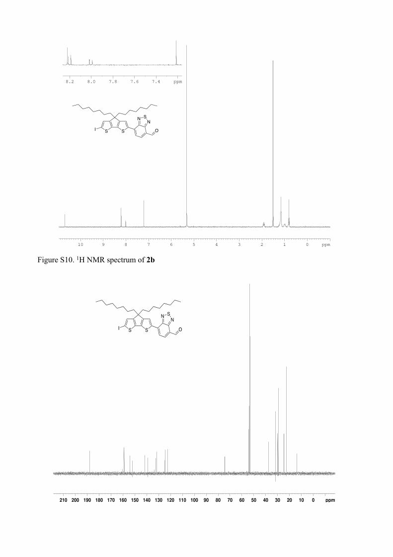
Figure S10. 1H NMR spectrum of 2b

Figure S11. 13C NMR spectrum of 2b
Figure S12. 1H NMR spectrum of 3b
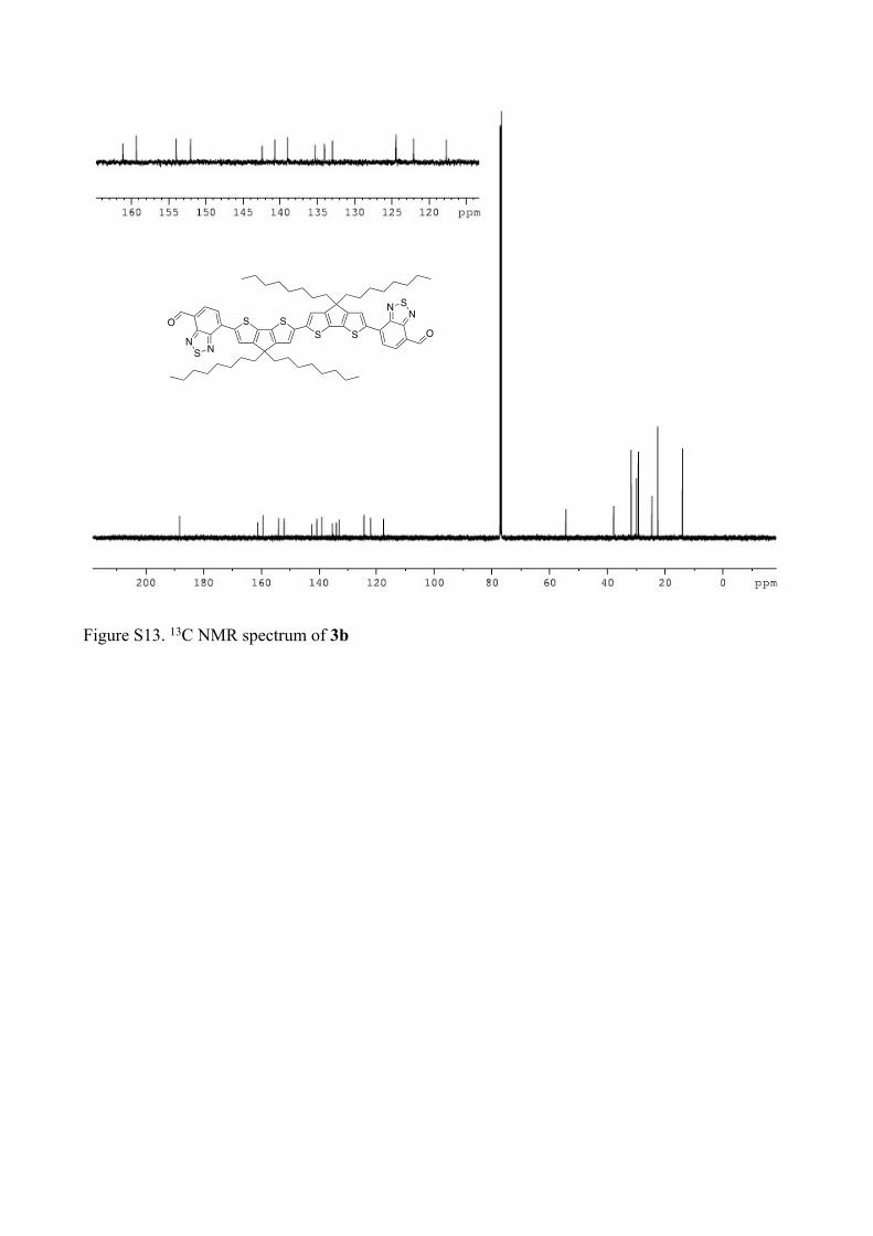
Figure S13. 13C NMR spectrum of 3b

Figure S14. 1H NMR spectrum of DA
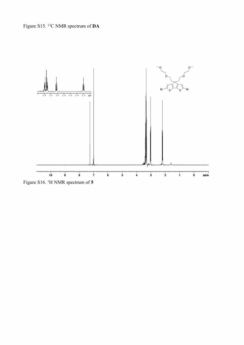
Figure S15. 13C NMR spectrum of DA
Figure S16. 1H NMR spectrum of 5

Figure S17. 13C NMR spectrum of 5
Figure S18. 1H NMR spectrum of PG

3. Differential Scanning Calorimetry (DSC)
a) b)
Figure S19. DSC thermograms of a) PG and b) PCPDTBT. Scan rate is 100 °C min-1

200 400 600 800 1000 12000.0
0.2
0.4
0.6
0.8
1.0
1.2
k
WL
JD59 as cast JD59 THF
200 400 600 800 1000 12000.0
0.2
0.4
0.6
0.8
1.0
1.2
k
WL
JD22 as cast JD22 THF dimers
monomers
WL
400 500 600 700 800 900 1000-0.1
0.0
0.1
0.2
0.3
0.4
0.5
0.6
0.7
kM
MG MA
dimers
monomers
WL
PCPDTBT PG
DG as cast DG THF anneal
DA as cast DA THF anneal
MG MA
Wavelength (nm)
Wavelength (nm) Wavelength (nm)
a) b)
c)
Figure S20. a) Solution absorption spectra of PG and PCPDTBT at the same weight/volume and
solid state extinction coefficients (k) as a function of wavelength (WL) for b) Monomers and c)
Dimers.
4. Photoluminescence spectra
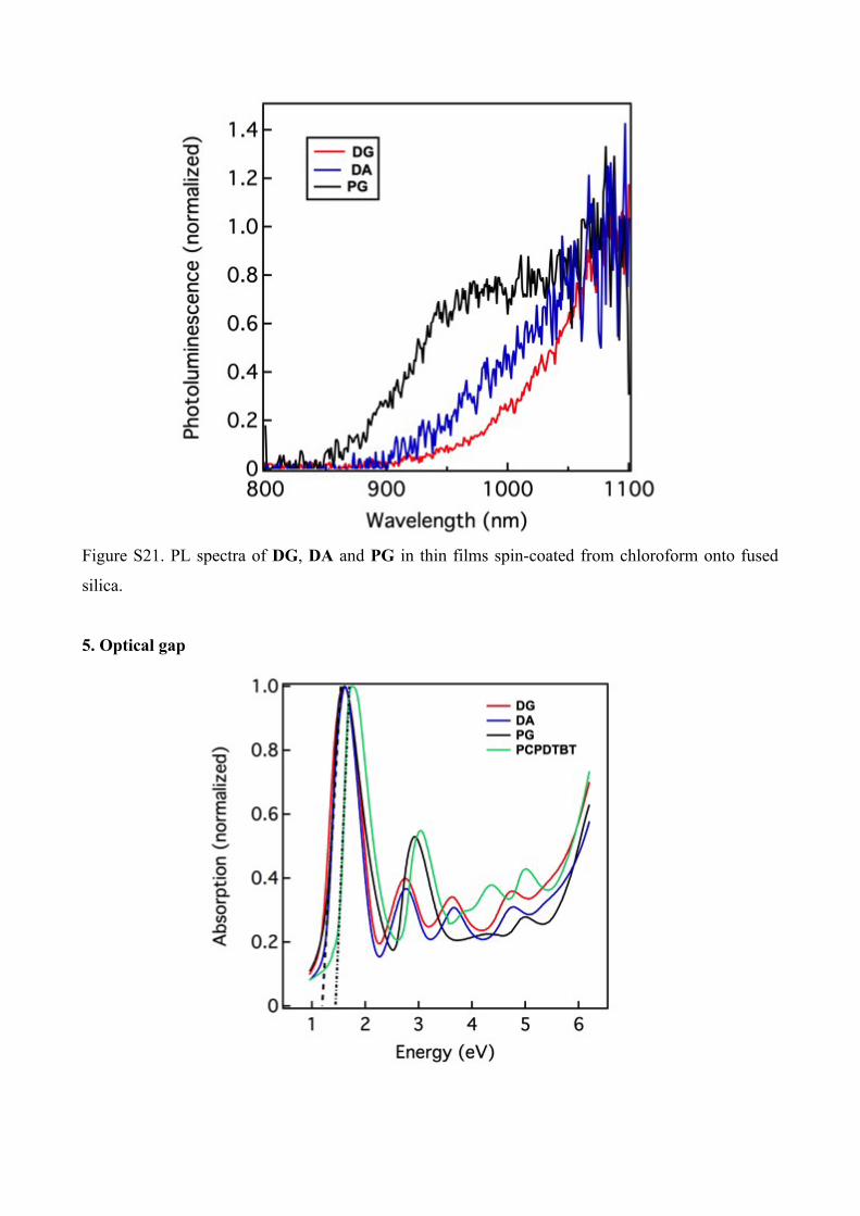
Figure S21. PL spectra of DG, DA and PG in thin films spin-coated from chloroform onto fused
silica.
5. Optical gap

Figure S22. Estimation of the optical gap of DG, DA and PG (~ 1.2 eV) and PCPDTBT (~1.5 eV)
in thin films spin-coated from chloroform onto fused silica.
6. X-ray analysis
Figure S23. Grazing-incidence diffractograms of a) DG and DA; b) PG and PCPDTBT films spin-
coated from chloroform onto silicon substrates. The red traces have been offset by a factor of 10 for
clarity.

Figure S24. XRR profiles and corresponding SLD versus thickness plots (inserts) for a) DA, b) DG,
c) PCPDTBT and d) PG. Individual points represent recorded data and solid black lines indicate
the fitting curves. Films were spin-coated from chloroform onto silicon substrates.
7. Cyclic voltammetry (CV)
a) b)
c) d)
Figure S25. Cyclic voltammograms (first reduction and oxidations - 10 cycles) of a) DG; b) DA; c)
PG and d) PCPDTBT.

8. SCLC
Hole/electron mobility measurements were conducted by measuring the Space-Charge-Limited-
Current (SCLC) and employing the Mott-Gurney law and Poole-Frenkel models:
𝐽 = 𝐸 + 98
ε0εr𝑉2
𝑑3 𝑒� 𝐸
𝐸0 ,
where 0, r, , E, , d and are the vacuum permittivity, relative permittivity, mobility, electric 𝐸0
field, conductivity, film thickness, and field dependence coefficient, respectively. The diode
structure ITO/MoOx/semiconductor/MoOx/Ag was used for hole only devices and
ITO/Al/semiconductor/Al for electron only devices.
Figure S26. Current density-Voltage (J-V) curves of a) electron only devices of DG and DA; b)
hole only devices of DG, DA, PCPDTBT and PG; c) electric field dependent mobility of DG and
DA and d) electric field dependent mobility of PCPDTBT and PG.

9. Homojunction OPV data
Figure S27. J-V curve for DG homojunction device with structure glass/ITO/PEDOT:PSS/DG (80
nm)/Sm/Al (PCE 0.3 %)
