electronic supplementaly information 18.2% with … 300 nmr spectrometer at ambient temperature....
TRANSCRIPT

Electronic Supplementaly Information
Pushing up the efficiency of planar perovskite solar cells to
18.2% with organic small molecular as electron transport layer
Pei-Yang Gu,a‡ Ning Wang,b‡ Chengyuan Wang,f Yecheng Zhou,a Guankui Long,a
Miaomiao Tian,a Wangqiao Chen,a Xiao Wei Sun,*, c Mercouri G. Kanatzidis*,e
Qichun Zhang,*,a,d
aSchool of Materials Science and Engineering, Nanyang Technological University, Singapore
639798
bSchool of Electrical and Electronic Engineering, Nanyang Technological University, Singapore
639798
cDepartment of Electrical and Electronic Engineering, College of Engineering, South University
of Science and Technology of China, Shenzhen 518055, P.R. China
dDivision of Chemistry and Biological Chemistry, School of Physical and Mathematical Sciences,
Nanyang Technological University, Singapore 637371
eDepartment of Chemistry, Northwestern University, 2145 North Sheridan Road, Evanston, IL
60208, USA.
fSchool of Chemistry, The University of Melbourne, Parkville, Victoria, 3010, Australia
Dr P.-Y Gu and Dr N. Wang contributed equally to this work.
S1
Electronic Supplementary Material (ESI) for Journal of Materials Chemistry A.This journal is © The Royal Society of Chemistry 2017

Contents
Scheme S1. Device architecture used in this work.
Figure S1.1H NMR spectrum of TDTP in CDCl3.
Figure S2. 13C NMR spectrum of TDTPin CDCl3.
Figure S3. HR-MS of TDTP.
Figure S4.1H NMR spectrum of PYPH in CDCl3.
Figure S5. 13C NMR spectrum of PYPHin CDCl3.
Figure S6. HR-MS of PYPH.
Figure S7.Cyclic voltammograms of (a) TDTP and (b) ferrocene in DCM solution.
Figure S8. (a) Normalized absorption of PYPH in DCM solution; (b) Cyclic
voltammograms of PYPH in DCM solution.
Figure S9. Absorption curves of pure perovskite and bilayer perovskite/TDTP thin
films
Figure S10. Typical SEM image of CH3NH3PbI3 perovskite thin film.
Figure S11. X-ray diffraction patternof CH3NH3PbI3 perovskite thin film used in this
work.
Figure S12.Three-dimensional AFM image ofbilayer perovskite/TDTP thin film.
Figure S13. Temperature and energy of a PYPH molecule on a 4 4 110-perovksite
surface in MD simulation.
Figure S14. The energy of a PYPH molecule on a 4 4 110-perovksite surface in
geometry optimizing simulation.
Table S1. Experimental electronic properties of TDTP and PYPH.
S2

Experimental Section
Materials: poly(3,4-ethylenedioxythiophene) polystyrene sulfonate (PEDOT:PSS,
Clevios P VP Al 4083) was purchased from H. C. Starck, Clevios GmbH. Phenyl-
C61-butyric acid methyl ester was purchased from NanoC and used as received.
Thiophene and 4,7-dibromobe-nzo[c][1,2,5]thiadiazole were purchased from Alfa
Aesar.1,10-Phenanthroline, 2-ethylhexyl bromide, trimethyltin chloride and n-
butyllithium were purchased from Sigma-Aldrich Company. 4,7-bis(5-(2-
ethylhexyl)thiophen-2-yl)benzo[c][1,2,5]thiadiazole-5,6-diamine was synthesized
according to the reported procedure.[1]Dichloromethane was distilled from calcium
hydride. Tetrahydrofuran was distilled from sodium. Other chemicals and solvents
were used directly without further purification.
Characterization: Using CDCl3 as solvents and tetramethylsilane (TMS) as the
internal standard, 1H NMR and 13C NMR spectra were measured on a Bruker
Advance 300 NMR spectrometer at ambient temperature. UV-Vis absorbance was
recorded on UV-Vis-NIR spectrometer Cary 5000. High resolution mass spectrum
(HRMS) was performed on a Waters Q-Tof premier mass spectrometer. Cyclic
voltammetry measurements were conducted on a CHI 604E electrochemical analyser
with glassy carbon (diameter: 1.6 mm; area: 0.02 cm2) as a working electrode, and
platinum wires as a counter electrode and a reference electrode, respectively. Fc+/Fc
was used as an internal standard. Potentials were recorded versus Fc+/Fc in a solution
of anhydrous dichloromethane (DCM) with 0.1 M
tetrabutylammoniumhexafluorophosphate (TBAPF6) as a supporting electrolyte at a
scan rate of 100 mV s-1. Employing empirical formulas ELUMO/HOMO= -[4.8-EFc +
Ere/oxonset] eV, where EFc= 0.24 V (measured in our setup), the value of HOMO or
LUMO can be calculated.
The surface morphology of TDTP thin film was analysed using atomic force
microscope (Park System Co.). The current density-voltage (J-V) of the solar cells
were measured using a Keithley 2400 source meter under simulated AM1.5
illumination (100 mW cm-2) by a Xenon-lamp-based solar simulator (Solar Light Co.
S3
Inc., USA). The light intensity was calibrated using a Si-reference cell certified by the
National Renewable Energy Laboratory, with the mismatch factor less than 2%. A
non-reflective mask (0.09 cm2) was used for defining the cell area. The external
quantum efficiency spectra were recorded with an EQE measurement system (PVE
300, Bentham, UK) comprised of a Xenon lamp, a momochoromator, a chopper, a
lock-in amplifier, and a calibrated silicon photodetector.
Device fabrication: The pre-patterned ITO (sheet resistance of 15 Ω sq-1, Lumtec,
Taiwan) patterned glass were cleaned ultrasonically with an alconox (detergent)
solution, followed by sonication in sequence with deionized water, acetone, and
isopropyl alcohol for 15 min each, then the substrates were dried using blowing
nitrogen gas. The ITO glasses are then UV-ozone treated for 20 mins prior to the
deposition of other layers. A ~30 nm-thick poly(3,4-ethylenedioxythiophene)
polystyrene sulfonate (PEDOT:PSS) hole transport layer was spun on the top of
indium tin oxide (ITO) glass substrate at 3000 rpm for 60 s in ambient conditions,
following an annealing treatment at 130 °C for 30 min in air. A 350 nm-thick
perovskite (CH3NH3PbI3) layer was spun on PEDOT:PSS hole transport layer in
glove box using 40 wt.% precursor with equal molar CH3NH3I and PbI2 in DMF
solution. The as-spun perovskite layer was annealed at 100 °C for 5 min to drive off
solvent and form the perovskite phase. Different thickness of TDTP was spun on top
of perovskite layer using a solution of TDTP in 1,2-dichlorobenzene. The thickness
of TDTP was carefully carried out using Alpha-Step D-600 Stylus Profiler (KLA-
Tencor Corporation). The device (active area: 3.2 mm × 3.2 mm) was completed by
the thermal evaporation of the LiF (1 nm)/Al(100 nm) electrode on the top.
Simulation details: The size of the unit cell is determined to avoid the interaction
between molecules and perovskite layers. The area of 25.284 25.029Å2 is the area of
a 44 110-perovksite surface. The 35.411Å height is set to avoid the interaction
between molecules and the other surface. Usually, the interaction cut-off distance
should be larger than 10Å. As shown in Figure 5, the distances between the molecules
and the other surface are 11.8 Å and 14.0 Å. The cut-off energy was 400 eV. The used
K-points just the point due to the huge unit cell. The ab initio molecular dynamic
S4
simulations temperature is 1000 K, the time interval is 1.0 fs, and the total simulation
time is longer than 500 fs, which depends on the energy variation. The PYPH and
TDTP absorption models include 538 and 527 ions, respectively.
Figure S13 shows the energy and temperature a PYPH molecule on a 4 4 110-
perovksite surface during the NVT MD simulations. The absorption system is
unstable before 150 fs and reached relative stable equilibrium after 400 fs. A low
energy configuration was chosen from MD process as the absorption configuration.
Then the chosen configuration was optimized. It converged very slowly due to the
very large model.
S5
Synthesis of 10,14-bis(5-(2-ethylhexyl)thiophen-2-yl)dipyrido[3,2-a:2',3'-
c][1,2,5]thiadiazolo[3,4-i]phenazine (TDTP)
A mixture of 4,7-bis(5-(2-ethylhexyl)thiophen-2-yl)benzo[c][1,2,5]thiadiazole-
5,6-diamine (554 mg, 1 mmol) and 1,10-phenanthroline-5,6-dione (210 mg, 1
mmol) in acetic acid (100 mL) was stirred at 118oC under nitrogen for 48 h.
After cooling to room temperature, the mixture was poured into methanol and
the crude product was purified by column chromatography over silica gel,
eluting with DCM/methanol to give green compound TDTP (378 mg,
0.52mmol, 52%).
1H NMR (300 MHz, CDCl3) δ 9.05 (t, J = 5.4 Hz, 4H), 8.41 (s, 2H), 7.40 (s, 2H), 6.57
(s, 2H), 2.67 (s, 4H), 1.58 – 1.18 (m, 18H), 1.05 – 0.88 (m, 12H).
13C NMR (75 MHz, CDCl3) δ 152.1, 150.5, 150.2, 148.8, 140.7, 135.2, 134.1,
133.8, 133.2, 127.4, 125.3, 123.6, 119.6, 41.4, 33.6, 32.7, 29.1, 25.6, 23.0, 14.3,
11.0.
HR-MS, calcd for C42H45N6S3, 729.2868; found, 729.2844.
Synthesis of 10,17-bis((triisopropylsilyl)ethynyl)dipyrido[3,2-a:2',3'-
c]quinoxalino[2,3-i]phenazine (PYPH)
PYPH was obtained as black powder in 57% yield from the reaction between
1,4-bis((triisopropylsilyl)ethynyl)phenazine-2,3-diamine and 1,10-
phenanthroline-5,6-dione by following the general procedure described for
TDTP.
1H NMR (300 MHz, CDCl3) δ 9.81 (d, J = 8.0 Hz, 1H), 9.31 (s, 1H), 8.29 (dt, J = 5.8,
2.9 Hz, 1H), 7.92 (dd, J = 6.9, 3.4 Hz, 1H), 7.81 (s, 1H), 1.43 (s, 21H).
13C NMR (300 MHz, CDCl3) δ 153.4, 149.4, 145.3, 143.5, 143.1, 141.9, 134.9,
132.2, 130.5, 127.8, 124.5, 123.0, 111.7, 102.4, 19.0, 11.8.
HR-MS, calcd for C46H53N6Si2, 745.3870; found, 745.3864.
S6

Scheme S1. Device architecture used in this work.
Figure S1.1H NMR spectrum of TDTP in CDCl3.
S7

Figure S2. 13C NMR spectrum of TDTP in CDCl3.
Figure S3. HR-MS of TDTP.
S8
Figure S4.1H NMR spectrum of PYPH in CDCl3.
Figure S5.13C NMR spectrum of PYPH in CDCl3.
S9
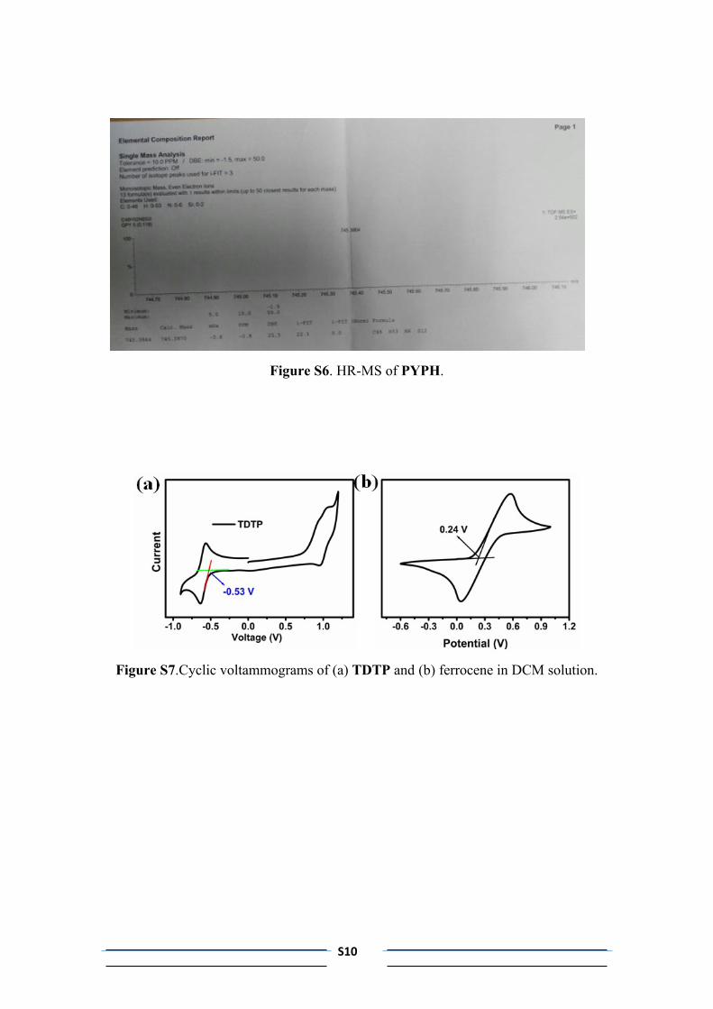
Figure S6. HR-MS of PYPH.
Figure S7.Cyclic voltammograms of (a) TDTP and (b) ferrocene in DCM solution.
S10

Figure S8. (a) Normalized absorption of PYPH in DCM solution; (b) Cyclic
voltammograms of PYPH in DCM solution.
Figure S9. Absorption curves of pure perovskite and bilayer perovskite/TDTP thin
films.
S11
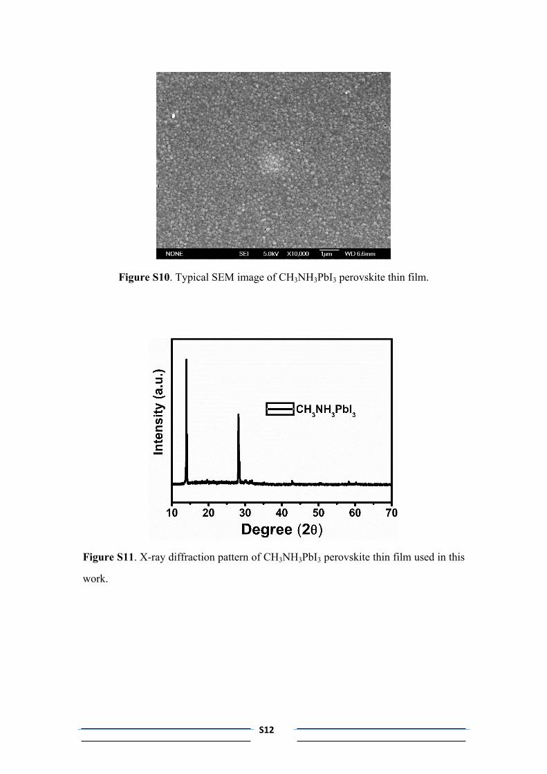
Figure S10. Typical SEM image of CH3NH3PbI3 perovskite thin film.
Figure S11. X-ray diffraction pattern of CH3NH3PbI3 perovskite thin film used in this
work.
S12

Figure S12. Three-dimensional AFM image of bilayer perovskite/TDTP thin film.
Figure S13. Temperature and energy of a PYPH molecule on a 4 4 110-perovksite
surface in MD simulation.
S13

Figure S14. The energy of a PYPH molecule on a 4 4 110-perovksite surface in
geometry optimizing simulation.
Table S1. Experimental electronic properties of TDTP and PYPH.
Compounds ELUMO (eV)a EHOMO (eV)b Egap (eV)c
TDTP -4.03 -5.44 1.41
PYPH -3.92 -5.80 1.88
aFrom CV: ELUMO = -[4.8-EFc + Ere/onset] eV (EFc= 0.24 V).bEHOMO = ELUMO - Egopt.cfrom
UV-vis.
S14

Figure S15. J-V curve of electron-only device with a device structure of
Glass/ITO/Al/PCBM/Ca/Al.
S15

Reference
1. P.-Y. Gu, J. Zhang, G. Long, Z. Wang, Q. Zhang, Journal of Materials Chemistry
C, 2016, 4, 3809 - 3814.
S16