electron transfer processes in -acceptor...
TRANSCRIPT

Electron transfer processes ina dye-TiO2/SnO2-acceptor assemblyTowards long lived charge separated states for solar fuels
Master’s thesis in Materials Chemistry
Jimmy Björklund
Department of Chemistry and Chemical EngineeringCHALMERS UNIVERSITY OF TECHNOLOGYGothenburg, Sweden 2016


Master’s thesis 2016:NN
Electron transfer processes ina dye-TiO2/SnO2-acceptor assembly
Towards long lived charge separated states for solar fuels
JIMMY BJÖRKLUND
Department of Chemistry and Chemical EngineeringDivision of Chemistry and Biochemistry
Physical Chemistry research groupChalmers University of Technology
Gothenburg, Sweden 2016

Electron transfer processes in a dye-TiO2/SnO2-acceptor assemblyTowards long lived charge separated states for solar fuelsJIMMY BJÖRKLUND
© JIMMY BJÖRKLUND, 2016.
Supervisor: Valeria Saavedra, Chemistry and Chemical EngineeringExaminer: Maria Abrahamsson, Chemistry and Chemical Engineering
Master’s Thesis 2016:NNDepartment of Chemistry and Chemical EngineeringDivision of Chemistry and BiochemistryPhysical Chemistry research groupChalmers University of TechnologySE-412 96 GothenburgTelephone +46 72 731 26660
Typeset in LATEXPrinted by [Name of printing company]Gothenburg, Sweden 2016
iv
Electron transfer processes in a dye-TiO2/SnO2-acceptor assemblyTowards long lived charge separated states for solar fuelsJIMMY BJÖRKLUNDDepartment of Chemistry and Chemical EngineeringChalmers University of Technology
AbstractWith increasing demands for carbon neutral fuels, an attractive solution is to de-velop solar fuel devices. The conversion efficiencies for solar fuel devices are currentlylow, which in part is due to the challenge of implementing multiple electron transfer(MET) reactions with the catalyst. This thesis has therefore investigated an hybridorganic-inorganic solar fuel assembly, which is capable of MET reactions. The ob-jective of this study has been to prove a conduction band mediated electron transferprocess from a semiconductor to an electron acceptor as a proof of principle for thissolar fuel assembly. This was achieved by performing photolysis and spectroelec-trochemical measurements on both TiO2 and SnO2 with hemin and hemin(py)2 aselectron acceptors respectively. In addition, this thesis has also been aimed towardsinvestigating the back electron transfer (electron recombination) which has a detri-mental effect on solar fuel assemblies. The electron recombination was investigatedon TiO2, SnO2 and on a mixed TiO2/SnO2 semiconductor system. This was studiedusing single wavelength nanosecond transient absorption spectroscopy. The resultsshowed no clear decrease in the rate of recombination by mixing the semiconductors,but more experiments are required to study this effect. With the electron accep-tor hemin(py)2 absorbed on the dye-sensitized semiconductor films, a significantlyslower rate of recombination was observed compared to semiconductor films with-out an electron acceptor. This was especially apparent in the region between 200and 1300 microseconds, which could potentially allow for photo catalytical reactionsto occur. Incorporation of a catalyst in dye-sensitized semiconductors could thuspossibly be advantageous for this type of solar fuel assembly.
Keywords: dye sensitized solar cell, solar fuels, electron recombination, mixed TiO2/SnO2semiconductor system, conduction band mediated electron transfer, cascade electrontransfer
v


AcknowledgementsFirst, I would like to thank Maria Abrahamsson for allowing me to be part of thisinteresting project, and all the support and feedback. I would also like to greatlythank Valeria Saavedra for all the help in the lab and always taking time to explainthings. In addition, I want to thank Elin Sundin for a very pleasant collaboration ofmaking of the semiconductor films, the support in the lab, and for all the fun times.Also, I would like to thank all the wonderful people in Maria’s research group forwelcoming me, and help with things in the lab. Finally, I would like to thank all theMaster’s Thesis students in the office, for all the good fika, and fun times.
Jimmy Björklund, Gothenburg, June 2016
vii


Contents
List of Figures xi
List of Tables xiii
1 Introduction 11.1 Background . . . . . . . . . . . . . . . . . . . . . . . . . . . . . . . . 11.2 Objective . . . . . . . . . . . . . . . . . . . . . . . . . . . . . . . . . 2
2 Theory 32.1 Quantum mechanics . . . . . . . . . . . . . . . . . . . . . . . . . . . 32.2 Light matter interaction . . . . . . . . . . . . . . . . . . . . . . . . . 42.3 Deactivation of excited states . . . . . . . . . . . . . . . . . . . . . . 4
2.3.1 Vibrational relaxation . . . . . . . . . . . . . . . . . . . . . . 62.3.2 Fluorescence and phosphorescence . . . . . . . . . . . . . . . . 62.3.3 Internal conversion and intersystem crossing . . . . . . . . . . 62.3.4 Excited state reactions . . . . . . . . . . . . . . . . . . . . . . 72.3.5 Lifetime of the excited state and quantum yield . . . . . . . . 7
2.4 Photoinduced electron transfer . . . . . . . . . . . . . . . . . . . . . . 72.4.1 Marcus theory . . . . . . . . . . . . . . . . . . . . . . . . . . . 8
2.5 Semiconductors . . . . . . . . . . . . . . . . . . . . . . . . . . . . . . 82.6 Hybrid organic-inorganic assemblies . . . . . . . . . . . . . . . . . . . 92.7 Electron recombination . . . . . . . . . . . . . . . . . . . . . . . . . . 112.8 System of study . . . . . . . . . . . . . . . . . . . . . . . . . . . . . . 12
2.8.1 TiO2 semiconductors . . . . . . . . . . . . . . . . . . . . . . . 132.8.2 Solvents and electrolytes . . . . . . . . . . . . . . . . . . . . . 14
2.9 Measurement techniques . . . . . . . . . . . . . . . . . . . . . . . . . 142.9.1 UV-vis Spectroscopy . . . . . . . . . . . . . . . . . . . . . . . 142.9.2 Steady state photolysis . . . . . . . . . . . . . . . . . . . . . . 142.9.3 Nanosecond-transient absorption spectroscopy . . . . . . . . . 15
2.9.3.1 Ground-state bleach . . . . . . . . . . . . . . . . . . 152.9.3.2 Excited state absorption . . . . . . . . . . . . . . . . 152.9.3.3 Product absorption . . . . . . . . . . . . . . . . . . . 16
2.9.4 Cyclic voltammetry . . . . . . . . . . . . . . . . . . . . . . . . 172.9.5 Spectroelectrochemistry . . . . . . . . . . . . . . . . . . . . . 172.9.6 Scanning electron microscopy . . . . . . . . . . . . . . . . . . 182.9.7 Energy dispersive X-ray spectroscopy . . . . . . . . . . . . . . 18
ix

Contents
3 Methods 193.1 Chemicals . . . . . . . . . . . . . . . . . . . . . . . . . . . . . . . . . 193.2 Equipment . . . . . . . . . . . . . . . . . . . . . . . . . . . . . . . . . 193.3 Preparation of semiconductor pastes . . . . . . . . . . . . . . . . . . 20
3.3.1 Failed synthesis of SnO2 paste . . . . . . . . . . . . . . . . . . 203.3.2 Mixed semiconductor films . . . . . . . . . . . . . . . . . . . . 20
3.4 Preparation of semiconductor films . . . . . . . . . . . . . . . . . . . 203.5 Experimental procedure . . . . . . . . . . . . . . . . . . . . . . . . . 21
3.5.1 Transient absorption spectroscopy . . . . . . . . . . . . . . . . 213.5.2 Steady state photolysis . . . . . . . . . . . . . . . . . . . . . . 223.5.3 Spectroelectrochemistry and cyclic voltammetry . . . . . . . . 223.5.4 UV-vis spectroscopy . . . . . . . . . . . . . . . . . . . . . . . 223.5.5 Data analysis . . . . . . . . . . . . . . . . . . . . . . . . . . . 22
3.5.5.1 Excited state decay fitting . . . . . . . . . . . . . . . 22
4 Results 234.1 Materials Characterization . . . . . . . . . . . . . . . . . . . . . . . . 23
4.1.1 Spectroscopic and electrochemical properties of Hemin . . . . 234.2 Conduction band mediated electron transfer . . . . . . . . . . . . . . 26
4.2.1 Photo induced band gap excitation in semiconductors . . . . . 264.2.2 Conduction band mediated transfer between semiconductor
and electron acceptor . . . . . . . . . . . . . . . . . . . . . . . 264.3 Recombination study of semiconductor systems . . . . . . . . . . . . 28
4.3.1 Excitation wavelength . . . . . . . . . . . . . . . . . . . . . . 284.3.2 Probe wavelength . . . . . . . . . . . . . . . . . . . . . . . . . 304.3.3 Quantification of photoinduced electron transfer rate using
transient absorption spectroscopy . . . . . . . . . . . . . . . . 304.3.3.1 The effect of solvents on electron recombination . . . 304.3.3.2 The effect of semiconductor systems on electron re-
combination . . . . . . . . . . . . . . . . . . . . . . . 31
5 Discussion 355.1 Conduction band mediated electron transfer . . . . . . . . . . . . . . 355.2 The effect of solvents on recombination . . . . . . . . . . . . . . . . . 365.3 The effect of semiconductor assemblies on recombination . . . . . . . 36
6 Conclusion 396.1 Future work . . . . . . . . . . . . . . . . . . . . . . . . . . . . . . . . 39
Bibliography 41
A Appendix 1 IA.1 EDX locations on SnO2/TiO2 film . . . . . . . . . . . . . . . . . . . . II
x

List of Figures
2.1 Molecular orbitals depicting one s, p and d orbital from left to right. . 42.2 Potential surface energy plots of two orbitals perfectly overlapping
and slightly overlapping in a) and b) respectively. The promotionof an electron from one orbital to another typically occur from thelowest vibrational state due to rapid vibrational relaxation. . . . . . . 5
2.3 Jablonski diagram depicting deactivation pathways inside a molecule. 52.4 Illustration of the Stokes shift . . . . . . . . . . . . . . . . . . . . . . 62.5 Schematic representation of the three regions of Marcus theory. From
left to right; the normal region, the activationless region and theMarcus inverted region. . . . . . . . . . . . . . . . . . . . . . . . . . . 9
2.6 Schematic illustration of the general principle of a hybrid organic-inorganic assembly for solar fuel production. . . . . . . . . . . . . . . 10
2.7 Schematic representation of photoinduced electron transfer and therecombination process. . . . . . . . . . . . . . . . . . . . . . . . . . . 11
2.8 Schematic representation of a semiconductor system with a physicalbarrier to prevent electron recombination . . . . . . . . . . . . . . . . 12
2.9 Schematic representation of the energy levels for D35CPDT, TiO2,SnO2, hemin and hemin(py)2. . . . . . . . . . . . . . . . . . . . . . . 13
2.10 Molecular structure of the dye D35CPDT and hemin illustrated in a)and b) respectively. . . . . . . . . . . . . . . . . . . . . . . . . . . . . 13
2.11 A general result obtained by a CCD camera and photodiode respectively 162.12 Schematic illustration of nanosecond transient absorption spectroscopy. 162.13 Illustrates a simple curve gained by cyclic voltammetry . . . . . . . . 172.14 Schematic illustration of spectroelectrochemistry. . . . . . . . . . . . 18
3.1 Schematic illustration of the doctor-blading technique. . . . . . . . . 21
4.1 SEM images produced with secondary electrons of semiconductorfilms made from SnO2 paste created by the hydrothermal method,and the method based on mixing, depicted from left to right respec-tively. The size of the nanoparticles can be estimated in the rangehundreds of nanometers to micrometers. . . . . . . . . . . . . . . . . 23
4.2 SEM images produced with secondary electrons of TiO2, SnO2 andmixed TiO2/SnO2 semiconductor films depicted from left to rightrespectively. The sizes of the nanoparticles are all estimated in therange of 10-30 nm. . . . . . . . . . . . . . . . . . . . . . . . . . . . . 24
xi

List of Figures
4.3 Cyclic voltammetry experiment performed on hemin in a solution of0.1M TBAPF2 and DMSO, purged with argon gas. CE = platina,RE = Ag/Ag+. The reduction potential of Fe3+/ Fe2+ was estimatedto -0.2 V vs Ag/Ag+. . . . . . . . . . . . . . . . . . . . . . . . . . . . 25
4.4 UV-vis spectroscopy measurement performed on hemin and hemintreated with pyridine in DMSO. A small redshift in absorbance forhemin treated with pyridine can be observed, which indicates a coor-dination of pyridine to hemin. . . . . . . . . . . . . . . . . . . . . . . 25
4.5 Photolysis experiment of TiO2 and SnO2 displaying broad absorptionfrom the conduction band between 400 and 1100 nm. . . . . . . . . . 26
4.6 Photolysis measurement depicting photo-induced reduction of heminon TiO2. . . . . . . . . . . . . . . . . . . . . . . . . . . . . . . . . . . 27
4.7 Spectroelectrochemistry measurement depicting reduction peaks ofhemin on TiO2 induced by stepwise increase in electric field potential(V). . . . . . . . . . . . . . . . . . . . . . . . . . . . . . . . . . . . . 27
4.8 Photolysis measurement depicting photo-induced reduction of hemin(py)2on SnO2. . . . . . . . . . . . . . . . . . . . . . . . . . . . . . . . . . . 28
4.9 Spectroelectrochemistry measurement depicting reduction peaks ofhemin(py)2 on SnO2 induced by a stepwise increase in electric fieldpotential (V). . . . . . . . . . . . . . . . . . . . . . . . . . . . . . . . 29
4.10 UV-vis spectra of D35CPDT, hemin and hemin(py)2 on TiO2. Theselected pump wavelength is indicated in the spectra by the blackarrow at 520 nm. . . . . . . . . . . . . . . . . . . . . . . . . . . . . . 29
4.11 UV-vis spectra of the oxidized dye D35CPDT, and the reduced elec-tron acceptors hemin and hemin(py)2. The chosen probe wavelengthis indicated by a black arrow at 700 nm. . . . . . . . . . . . . . . . . 30
4.12 Transient absorption measurements of D35CPDT on TiO2 films inacetonitrile and DMSO with and without methanol. . . . . . . . . . . 31
4.13 Transient absorption measurements of D35CPDT on SnO2 films inDMSO and acetonitrile with methanol added to both solutions. . . . 32
4.14 Transient absorption measurements of D35CPDT on different semi-conductor systems with and without an electron acceptor. The slightlystepwise decay observed for the green and orange curve, is an artifactattributed to poor settings of the oscilloscope. . . . . . . . . . . . . . 33
A.1 Autoreduction of hemin on TiO2 performed in DMSO with 0,1MTBAPF6 in a dark room. . . . . . . . . . . . . . . . . . . . . . . . . . I
A.2 Autoreduction of hemin(py)2 on TiO2 performed in DMSO with 0,1MTBAPF6 in a dark room. . . . . . . . . . . . . . . . . . . . . . . . . . II
A.3 SEM image of the location of spectrum 1. . . . . . . . . . . . . . . . IIA.4 SEM image of the location of spectrum 2. . . . . . . . . . . . . . . . IIIA.5 SEM image of the location of spectrum 3. . . . . . . . . . . . . . . . III
xii

List of Tables
3.1 Time and temperature program in oven for TiO2, SnO2 and TiO2/SnO2semiconductor films. . . . . . . . . . . . . . . . . . . . . . . . . . . . 21
4.1 Summary of elemental analysis performed with EDX at three differentpoints. The results are reported in atomic %. . . . . . . . . . . . . . 24
4.2 Table of rate constants obtained from curve fitting with a biexponen-tial function. The parameters A1 and A2 have for convenience beenconverted into % to easier describe the amount of recombination oc-curring with each individual recombination processes. . . . . . . . . . 32
xiii

List of Tables
xiv

1Introduction
1.1 Background
With global warming emerging as an increasing risk to humanity and environmentalike, the need for drastic measures against carbon dioxide emissions are crucial.One of the most promising carbon neutral energy sources would be to harvest solarenergy because of its vast potential. Only the solar energy intercepting earth in onehour alone (4.1 ∗ 1020J) would be sufficient to sustain all of earth’s energy demandsfor an entire year. Naturally it is not feasible to believe that we can harvest all thatenergy. However to merely sustain earth’s global energy demands, estimated for thelate part of this century, would only equate to a small 0.16 % of earths area usingsolar cells of 10 % efficiency. [1]Despite this vast potential in solar energy, only a very small fraction of our cur-rent energy comes from solar energy, both in terms of electricity and fuels. Whilethere at present is a large focus on developing solar energy technologies for gener-ating electricity and heat, the bulk of energy are consumed as fuels [2]. There isthus a strong incentive to develop carbon neutral fuels. An ideal process, alreadyexisting in nature is the photosynthesis, which converts carbon dioxide and waterinto carbohydrates. While very impressive, it is also a slow process [3]. As a conse-quence, there have been many attempts to create artificial photosynthesis to achievehigher efficiency [4] [5]. In addition more chemical approaches to produce hydrogen,methane and methanol as viable fuels have also been tried.[6]An altogether different approach of converting carbon dioxide into fuels such asmethane or methanol have been tried without harvesting light, but by using an ex-ternal applied current to drive the reaction [7]. This process however have provendifficult due to the many reaction steps and redox equivalents it takes to completethe process. The process is further impeded by the formation of unstable interme-diates, which rapidly reverse to a more stable form by dissipating its energy andelectrons to its environment. This process therefore leaves much to be desired bothin terms of thermodynamics and kinetics. Typically, in order to create a viable fuelfrom carbon dioxide, multiple electron transfer (MET) reactions are necessary. Asthe name implies, multiple electrons are transferred in a near simultaneous step,which reduce the number of unstable intermediates formed, and increase the con-version efficiency.[2]One particular way of facilitating MET reactions would be to use the principles ofa dye sensitized solar cell (DSSC). In addition to a likely increase of the conversionefficiency, the process would also be powered by solar energy from the visible spectra
1

1. Introduction
making it entirely carbon neutral.
1.2 ObjectiveThe objective of this master’s thesis has been to investigate the electron transferprocesses in a hybrid organic- inorganic solar fuel assembly. More specifically, thisthesis has been primarily aimed towards proving a conduction band mediated elec-tron transfer from the conduction band of TiO2 and SnO2 to an electron acceptor,and investigating the rate of back electron transfer (electron recombination) in amixed TiO2/SnO2 semiconductor system. By introducing a second semiconductorof lower conduction band energy level to the system, a lower thermodynamic drivingforce for recombination is proposed to occur. Additionally the electron injection ef-ficiency has often been shown to increase in systems with electron transfer occurringin multiple steps. The methods used to study conduction band mediated electrontransfer in this thesis have been spectroelectrochemistry, and photolysis. The rateof recombination has been measured with a nanosecond transient absorption spec-troscopy.
A part of this thesis has also been dedicated towards optimization of preparation ofSnO2 semiconductor paste and making of TiO2, SnO2 and TiO2/SnO2 semiconduc-tor films. This has included characterization of the semiconductor films using scan-ning electron microscope (SEM), in terms of nanoparticle size, distribution and alsoinvestigating the composition with electron dispersive X-ray spectroscopy (EDX).In addition, the semiconductor films sensitized with a dye or electron acceptor hasalso been characterized with cyclic voltammetry (CV), UV-vis spectroscopy, spec-troelectrochemistry and photolysis.
2
2Theory
This part aims to provide a detailed understanding of the physical processes oc-curring inside solar cell devices for fuel production. This will include some basicquantum mechanics in order to discuss the kinetics of these electron and energytransfer mechanisms. Furthermore the basic design principle for hybrid inorganic-organic assemblies for solar fuel production will also be explained.
2.1 Quantum mechanicsClassical mechanics has certain limitations and cannot properly explain the waveparticle duality, or light matter interaction. As a result when studying photoinducedreactions, quantum mechanics becomes necessary.A fundamental cornerstone in quantum mechanics is the Schrödinger equation. Thisequation models elementary particles from their fundamental energies (potential andkinetic energy) in order to describe their interaction with each other. With a math-ematical definition of the interactions of elementary particles inside a system, thewave particle duality is possible to solve. This can be achieved by describing elec-trons in molecular orbitals with wave functions. By solving the (time independent)Schrödinger equation defined below in equation 2.1, i.e. determining the function ϕ,these molecular orbitals can be calculated and visualized in three dimensional plots,see figure 2.1[8].
Hϕ = Eϕ (2.1)H is defined as the Hamilton operator and describes the total energy in the system(see equation 2.2), ϕ the quantized solution to the Schrödinger equation and pro-portional to the probability of finding an electron in a certain position by |ϕ|2, andE as the energy of the corresponding molecular orbital.
H = −~2
2
N∑n=1
1mn
∇2n + V (r1, r2, ...rn, t) (2.2)
To solve the time independent Schrödinger equation even with several approxima-tions for more than a few particles, requires immense computing capabilities as theproblem becomes exponentially more complex with more particles. Thus quantummechanics is far from ideal when dealing with systems on a macro level. However forinvestigating the principles of photoinduced electron transfer and light matter inter-action, the system can be limited to a small number of particles and the Schrödingerequation can be managed relatively easy.
3

2. Theory
s py dxz
Figure 2.1: Molecular orbitals depicting one s, p and d orbital from left to right.
2.2 Light matter interactionLight is a form of electromagnetic radiation which can interact with charged particlesthrough its oscillating electric field component. Absorption of light may occur onlyif the magnitude of the electric field component matches the energy between twomolecular orbitals to facilitate the transition of an electron to the higher energy level2.3. [8]
E = hc
λ(2.3)
In order to explain the energy gap between different orbitals, one needs to considerthe initial and final state with the Schrödinger equation. A common way of visual-izing the energy gap is by a potential surface energy plot, in which the solution toSchrödinger’s equation, ϕ, is plotted against its nuclear coordinates. From this plot,the energy gap can be interpreted as the vertical distance between the initial andfinal state (Franck Condon principle). By comparing the vertical distance betweenperfectly matched orbital functions and slightly overlapping orbitals in figure 2.2aand 2.2b respectively, the energy gap can be observed to be larger for the latter.The energy gap is thus dependent on the orbital overlap, which helps explain whysome transitions occur more frequently than others.[8] [9]
2.3 Deactivation of excited statesOnce an electron has been promoted to an electronically excited state it can dis-sipate its energy by one of several deactivation pathways, or even a combinationof them. Typically the deactivation pathways of these processes are characterizedusing a Jablonski diagram, see figure 2.3.In addition to the electronic energy levels, there exist vibrational energy levels whichconsists of periodic quantized motions of the molecule. The energy gap between vi-brational energy states are however relative to the electronic energy levels muchsmaller.[9] The most fundamental deactivation pathways in an excited molecule
4

2. Theory
(a) (b)
Figure 2.2: Potential surface energy plots of two orbitals perfectly overlapping andslightly overlapping in a) and b) respectively. The promotion of an electron fromone orbital to another typically occur from the lowest vibrational state due to rapidvibrational relaxation.
are vibrational relaxation, fluoroescence, phosporescence, internal conversion, in-tersystem crossing and excited state reactions, which are explained in more detailbelow.
S1 S10
S2 S20
S3 S30
S0 S00S01S02S03
S11S12S13
S14
S15S16S21
S22
Singlet
T0T00
T1T10
T2T20
T01T02T03
T11T12T13
T21
Triplet
Absorption
Fluorescence(fast)
Phosphorescence(indirect, slow)
Vibrational relaxationIntersystem crossing
Internal conversion
Figure 2.3: Jablonski diagram depicting the deactivation pathways inside amolecule. For clarity the spin singlet states (S) and the triplet states (T ) havebeen separated. In addition, the excited and the vibrational sublevels are drawn bysolid and dashed horizontal lines respectively.
5

2. Theory
2.3.1 Vibrational relaxationThe transition between an electronically excited state to the lowest vibrational en-ergy level, is called vibrational relaxation. Since the energy from the excited stateis only transferred to a vibrational sublevel in the same orbital, the energy is dissi-pated as vibrational energy to the surrounding.[8]The kinetics of vibrational relaxation is rapid and relative to the process of emission(see 2.3.2) much faster. As a consequence of this, emission will as a rule alwaysoccur from the lowest vibrational energy level. An additional consequence of rapidvibrational relaxation, is the occurrence of the Stoke’s shift, which is the differencebetween absorption and emission wavelength.[9]
Figure 2.4: Illustration of the Stokes shift
2.3.2 Fluorescence and phosphorescenceThere are two radiative deactivation processes that may occur inside a molecule,which are differentiated by the multiplicity of the energy levels involved in the tran-sition. The transition between two energy levels of the same multiplicity, for exampletwo singlet levels, is known as fluroescence, whereas between different multiplicityis known as phosphorescence. Since the transition between two singlet energy statesprovide no constraint on the spin, the process is relatively fast. However for phospho-rescence, which may occur between a triplet and a singlet state, the spin momentumcannot be conserved in the transition between the two energy levels. This makesit a so called forbidden process, which however only translates into slow kinetics asthe spin may be changed by spin-orbit interaction with the nucleus [10]. [8]
2.3.3 Internal conversion and intersystem crossingThe energy level in one orbital can potentially match a high vibrational energy levelof a lower orbital. If transition between these orbital energy states have the samemultiplicity, the process is known as internal conversion. A consequence of internalconversion is the relaxation process after the transition, which occur from a highvibrational energy level to low vibrational state through vibrational relaxation. Theprocess is thus non radiative. Similar to internal conversion, the crossing betweenenergy levels of different multiplicity is also known as intersystem crossing.[9]
6

2. Theory
2.3.4 Excited state reactionsAn excited molecule can often as a result of its increased energy react with neighbor-ing molecules. This interaction can in the process of reaction consume the energyfrom the excited state and result in new molecular species. This process is alsoknown as quenching. While considering which molecules that may or may not in-teract with an excited species, it often helps to think of it as an entirely new speciesdifferent from its ground state. This due to the excited state not only has an en-hanced reactivity from its higher energy state, but also a changed electron structurewhich may make certain interactions possible.[9]
2.3.5 Lifetime of the excited state and quantum yieldThe deactivation pathways of an excited molecule can occur by any of the abovementioned deactivation processes. However to truly understand the behaviour of anexcited molecule, the kinetics of these processes must be considered [11].The expected lifetime of an excited molecule, τ (A∗), can be modelled by a firstorder kinetic reaction, see equation 2.4.
τ(A∗) = 1(kr + knr + kp)
(2.4)
[A∗] is the excited state, kr, the rate constant of radiative processes, knr the rateconstant for non radiative processes (not including excited state reactions), and kpthe rate constant of excited state reactions.A very useful concept in understanding the efficiency of a specific process is thequantum yield. The quantum yield is defined as the number of excited moleculesundergoing a specific process divided by the total amount of excited molecules fora given amount of time, see equation 2.5. [8][9]
ηi(A∗) = ki∑i ki
= kiτi(A∗) (2.5)
2.4 Photoinduced electron transferThe phenomenon photoinduced electron transfer is the transfer process of an elec-tron between a donor and an acceptor in which either exist in an electronicallyexcited state. Photoinduced electron transfer is technically a chemical deactivationprocess and the desired deactivation pathway of solar fuel devices. This is due toits ability to induce a charge separated state, which is a key function in all solar celldevices.[9][8]The electron transfer between a donor and an acceptor does not have to be betweentwo different molecules, but can also occur inside one large molecule of two moi-eties functioning as donor and acceptor. The process of intra-, and intermolecularphotoinduced electron transfer are very similar, and only becomes possible whenthe molecule has been electronically excited with a sufficiently long lifetime for thetransfer mechanism to compete with other deactivation pathways. For intermolec-ular photoinduced electron transfer the lifetime must also be approximate to the
7

2. Theory
time between collisions of neighboring molecules. The general reaction formula forphotoinduced electron transfer can be seen below in equation 2.6. [9]
D | A hυ−→ D∗ | A kET−→ D+ | A− (2.6)The possible applications for photoinduced electron transfer are many, for instanceit can be used to prevent luminescence and reactivity, or induce chemical changesor even induce luminescence from species that normally do not absorb light at thespecific wavelength.[9]
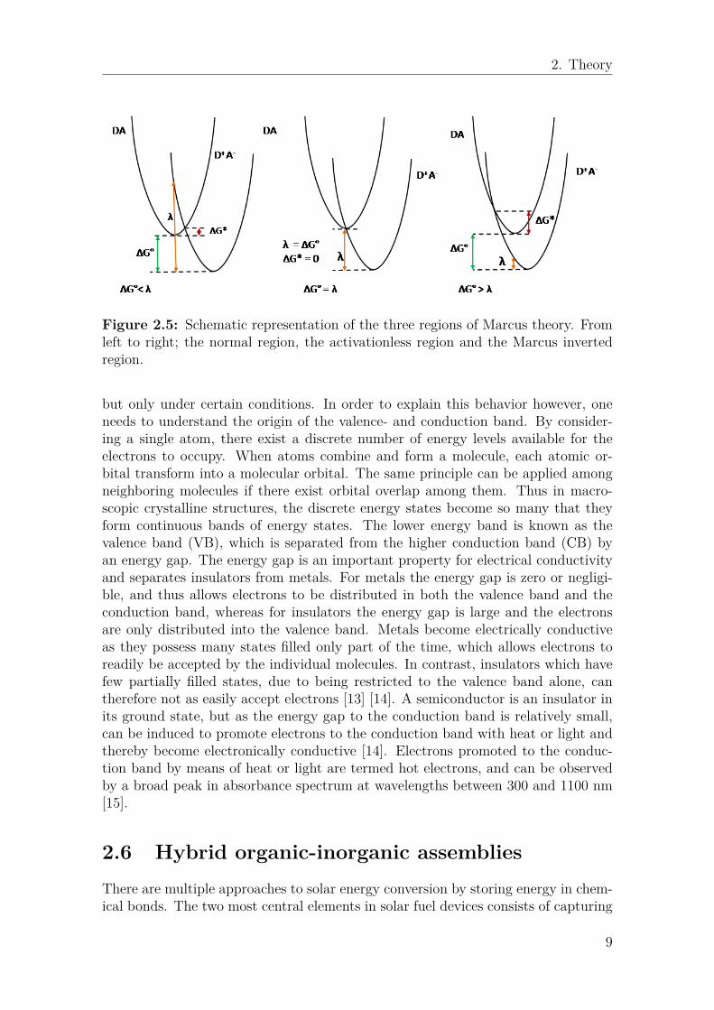
2.4.1 Marcus theoryIn order to understand and quantify the rate of photoinduced electron transfer, Mar-cus theory is typically necessary. In Marcus theory, the initial and final state of a re-action are investigated using potential surface energy plots gained from Schrödinger’sequation. However for simplicity, the solutions can be approximated to parabolicfunctions representing the initial donor acceptor complex, and the final charge sep-arated state, see figure 2.5.[12]
In Marcus theory the initial and final state is separated by an intermediate transi-tion state, which in figure 2.5 can be seen as the point of intersection between thetwo parabolic functions. The energy at the intersection point relative to the initialstate determines the activation energy of the reaction, which if positive needs to besupplied for the reaction to occur. In addition to the activation energy, the rate ofphotoinduced electron transfer is dependent on the reorganisational changes (λ) ofsurrounding molecules which must take place to find a new equilibrium, in order tobalance the electrostatic force from nuclei distortions and changed polarisation. Therate of photoinduced reaction can be seen below in equation 2.7, where υN is definedas the average nuclear frequency factor, κel the electronic transmission coefficientand ∆G0 the activation energy.[9] [12]
ket = υNκelexp(−(∆G0 + λ)2
4λRT ) (2.7)
From the above equation, three different regions can be characterized; the normal-ized region, the activationless region and Marcus inverted region denoted 1 to 3respectively below.
1. A region of small activation energy, which increase the rate of photoinducedelectron transfer with increasing driving forces.
2. A region of negligible activation energy, in which a change in driving force onlyinduce small changes in photoinduced electron transfer rate.
3. A region of strongly exergonic processes, in which the transfer rate is onlydecreasing with increasing driving force (Marcus inverted region). [9]
2.5 SemiconductorsA semiconductor constitutes the middle ground of electrical conductivity of insu-lators and metals. Unlike the insulator, the semiconductor can conduct electricity
8
2. Theory
Figure 2.5: Schematic representation of the three regions of Marcus theory. Fromleft to right; the normal region, the activationless region and the Marcus invertedregion.
but only under certain conditions. In order to explain this behavior however, oneneeds to understand the origin of the valence- and conduction band. By consider-ing a single atom, there exist a discrete number of energy levels available for theelectrons to occupy. When atoms combine and form a molecule, each atomic or-bital transform into a molecular orbital. The same principle can be applied amongneighboring molecules if there exist orbital overlap among them. Thus in macro-scopic crystalline structures, the discrete energy states become so many that theyform continuous bands of energy states. The lower energy band is known as thevalence band (VB), which is separated from the higher conduction band (CB) byan energy gap. The energy gap is an important property for electrical conductivityand separates insulators from metals. For metals the energy gap is zero or negligi-ble, and thus allows electrons to be distributed in both the valence band and theconduction band, whereas for insulators the energy gap is large and the electronsare only distributed into the valence band. Metals become electrically conductiveas they possess many states filled only part of the time, which allows electrons toreadily be accepted by the individual molecules. In contrast, insulators which havefew partially filled states, due to being restricted to the valence band alone, cantherefore not as easily accept electrons [13] [14]. A semiconductor is an insulator inits ground state, but as the energy gap to the conduction band is relatively small,can be induced to promote electrons to the conduction band with heat or light andthereby become electronically conductive [14]. Electrons promoted to the conduc-tion band by means of heat or light are termed hot electrons, and can be observedby a broad peak in absorbance spectrum at wavelengths between 300 and 1100 nm[15].
2.6 Hybrid organic-inorganic assembliesThere are multiple approaches to solar energy conversion by storing energy in chem-ical bonds. The two most central elements in solar fuel devices consists of capturing
9

2. Theory
light, and inducing formation and breaking of bonds for energy storage. The proper-ties required for these elements are however different and often difficult to combine.One solution to this problem, is to use the principles of the dye sensitized solar cell(DSSC), which separates the functions of capturing light to the dye-semiconductorinterface, and the charge carrier transfer to the semiconductor-electrolyte [16]. Bymaking small adjustments to the design of a DSSC, a device capable of driving aphotocatalytic reaction instead of outputting electricity can be made. The hybridorganic-inorganic solar fuel assembly is one design based on the DSSC, and is alsothe main focus in this thesis, see figure 2.6.The hybrid organic-inorganic solar fuel assembly, consists of a dye, a semiconductor,a catalyst and a redox couple, not including the chemical reactants and productsparticipating in the catalytic reaction [16]. The TiO2 semiconductor has a wideband gap of approximately 3.2 eV [17], which enables band gap excitation with UVlight. However since a large portion of the light emitted from the sun occurs in thevisible region, a dye can be added to increase the efficiency of the solar fuel assembly.Once the dye has been photoexcited to its lowest unoccupied energy level (LUMO),it can inject the electron into the conduction band of the semiconductor. For theinjection to be efficient however, it is important to have a good electronic couplingbetween the dye and acceptor, in addition to the conduction band being lower inenergy level relative to the excited state of the dye. Once the electron has beeninjected into the conduction band it can travel through the semiconductor to thecatalyst, whereupon the catalyst can absorb multiple electrons to reach a highly re-duced state. The catalyst will then have the possibility to facilitate multiple electrontransfer in a reaction with carbon dioxide and water to form methane or methanol.However in order to balance the charges caused by oxidizing the dye and reducingthe carbon dioxide a redox couple or sacrificial donor is also required. As the aim ofthis thesis is to study electron recombination, no redox couple have been includedin the experimental system.[16] [18]
Figure 2.6: Schematic illustration of the general principle of a hybrid organic-inorganic assembly for solar fuel production. This image was adapted from [19].
10

2. Theory
2.7 Electron recombinationAs described above in the hybrid organic- inorganic assemblies section, light in thevisible spectrum can be captured by a photosensitizer to induce an electronicallyexcited state. The electron injection from the excited state of the dye to the conduc-tion band of the semiconductor however occur in competition with other deactivationprocesses, see section 2.3. One way of achieving a high electron injection efficiencyand long life times of charge separated state has been shown by transferring the elec-trons in many small energy steps, a process also known as cascade electron transfer[18]. In addition to losses induced by poor electron injection, electron transfer isnot limited to the forward direction alone, but may also occur in the backwardsdirection. This electron transfer is commonly referred to as electron recombination,and may for instance occur from the conduction band of the semiconductor to theground state of the oxidized dye, see figure 2.7. For solar fuel devices, electron re-combination impose an efficiency limiting effect, as the backwards electron transferoften competes on approximately the same time scale as electron transfer in theforward direction [20].
Figure 2.7: Schematic representation of photoinduced electron transfer and therecombination process.
The exact efficiency limiting effect is determined by the relative rate difference ofthe forward and the backwards electron transfer. Since the physics of backwardselectron transfer is the same as electron transfer in the forward direction, Marcustheory can be applied in order to predict and minimize the rate of recombination.For instance, if electron transfer occurs in the normal region described by Marcustheory, using a semiconductor of lower conduction band energy level would likelydecrease the rate of recombination. Thus the idea of combining two semiconductorsto achieve a cascade electron transfer and utilizing a conduction band of low energycould theoretically have a positive effect. Nonetheless, electron transfer processesoccurring in the Marcus inverted region have been observed [21] [22] [23]. In addition
11

2. Theory
any positive effect from using a semiconductor of lower energy will also have tobe weighed against the disadvantage of eliminating certain catalysts for multipleelectron transfer reactions.An altogether different approach of minimizing the electron recombination can beachieved by introducing a barrier for backwards electron transfer to induce a longlived charge separated state [20]. In a system with two semiconductors, this can beachieved by physically separating the dye from the semiconductor of lower energylevel, see figure 2.8. Thus the electron recombination from the semiconductor oflower energy level must pass through the semiconductor of higher energy, which isthermodynamically not allowed.
Figure 2.8: Schematic representation of a semiconductor system with a physicalbarrier to prevent electron recombination
2.8 System of studyWith the main focus of this study being the effect on recombination for differentsemiconductor systems, the experimental system of study could be reduced to asimple assembly consisting of a dye, a semiconductor and an electron acceptor. Forthis project, an organic dye named D35CPDT was chosen, due to its known com-patibility with the semiconductors in terms of chemical adhesion and energy levels,see figure 2.10a. The choice of electron acceptor was a somewhat more problematicchoice for this study, as the relatively high reduction potential of SnO2, see fig-ure 2.9 and requirement to adhere to both TiO2 and SnO2 excludes many electronacceptors. The electron acceptor Fe-PPIX, also more commonly known as hemin,see figure 2.10b, was ultimately chosen due to its success as an electron acceptor onTiO2, and a reduction potential close to SnO2, which could allow reduction of heminon SnO2 depending on environment. A contributing factor for selecting hemin, wasalso the possibility of coordinating pyridine to hemin to form hemin(py)2 with amore positive reduction potential. This coordination would ensure at least one elec-tron acceptor suited for SnO2, in addition to the possibility of studying electronrecombination with two different electron acceptors.
12

2. Theory
Figure 2.9: Schematic representation of the energy levels for D35CPDT [24], TiO2[20], SnO2 [20], hemin [25] and hemin(py)2 [26].
(a) D35CPDT (b) hemin
Figure 2.10: Molecular structure of the dye D35CPDT and hemin illustrated ina) and b) respectively.
2.8.1 TiO2 semiconductors
TiO2 exist naturally in three different crystalline phases, anatase, rutile and brookite,of which rutile is the most stable and anatase the most chemically active phase.Mesoporous TiO2 with an anatase structure has for over two decades yielded thehighest efficiency in dye sensitized solar cell devices, and is still the most heavilyused semiconductor for research and commercial applications.
13

2. Theory
2.8.2 Solvents and electrolytesAs part of the study of recombination on different semiconductor systems, the effectof solvents have been included as these may influence the energy levels of the solarassembly components and thus impact the efficiency. The solvents investigated aredimethyl sulfoxide (DMSO) and acetonitrile (MeCN), with and without addition ofmethanol. Methanol is a known electron hole scavenger [27], which theoreticallymay donate electrons to holes in the conduction band or to the ground state of theexcited dye to inhibit recombination.
2.9 Measurement techniques
2.9.1 UV-vis SpectroscopyThe principles of UV-vis spectroscopy is based on the unique characteristic energylevels of different molecules, which allows absorption at different wavelengths. Byusing a continuous white light source, and using a prism or diffraction grating, thelight can be divided into monochromatic wavelengths [28]. The monochromatic lightcan then be further divided into two separate beams, with one of them working asa reference. Then, by directing one beam through the sample, and measuring theintensity of this beam relative to the reference, information about the absorptioncan be gained. The exact absorbed amount can be calculated from Lambert Beer’sLaw, see equation 2.8 below.
A = log(I/I0) =∑i
ε(λ) l ci (2.8)
A is defined as the absorbance, and I and I0 as the intensity of sample and referencerespectively. Epsilon, ε, as the extinction coefficient, l as the optical path length,and c as the concentration of a specific unit.
One application of UV-vis spectroscopy is performing repeated measurements atdifferent times in order to gain information about possible chemical reactions takingplace. By plotting the spectra in the same graphs, the relative difference of thepeak intensities can be observed and used to indicate if a chemical species havebeen consumed or produced. In addition, the presence of wavelengths with con-stant absorption over time (isosbestic point), may also provide information aboutthe chemical reactions. A typical example of an isosbestic point is in a system wherea reactant and a product have the same extinction coefficient, ε(λ), at that specificwavelength. The disappearance of an isosbestic point could then indicate that thereno longer is only one reactant and product in the system. [29]
2.9.2 Steady state photolysisSteady state photolysis is a technique combining an external light source with UV-vis spectroscopy. The addition of an external light source can be used to investigatea specimen’s interaction with light, to either prevent or induce chemical reactions.[29]
14

2. Theory
2.9.3 Nanosecond-transient absorption spectroscopyThe idea of nanosecond transient absorption spectroscopy (TAS) is to study ex-cited state decay or excited state reactions occurring on the micro to nanosecondtimescale. This instrument is an important tool to study the electron recombinationprocesses in photosynthetic systems, which typically occur on these timescales.The principle of transient absorption spectroscopy is based on repeated light ab-sorption measurements performed on a single sample, where a change in absorptioncorresponds to a changed electronic structure of a chemical species (Lambert Beer’slaw). Thus, by exposing the sample to a laser pulse and studying the induced ab-sorption changes, information about photoinduced electron transfer processes canbe obtained. [9]The instrument functions by generating a pulsed laser light in an oscillator whichpass through an optical parametric oscillator (OPO) to achieve the appropriatewavelength, see figure 2.12. The wavelength should be consistent with the energyrequired for ground state excitations of the molecule to be investigated. This beamis also called the pump beam. Perpendicular to this beam, a white light sourceis used to measure the absorbance of the sample, typically in the range of 400 -1100 nm depending on the molecule investigated. The intensity of the beam can bemeasured by a charge coupled device (CCD) camera. From the measured intensityit is possible to calculate the differential absorption ∆A from equation 2.9. Thesignal of the differential absorption can be either negative or positive depending onwhat energy transfer process occur, see figure 2.11. [9] [11]The three most general processes include ground-state-bleaching, excited state ab-sorption and product absorption, which are described in more detail below. For aquantitative analysis of the kinetics of energy transfer processes occurring in photo-synthetic systems, like recombination, a photodiode can be used as a detector insteadof a CCD camera. The output signal then, unlike the CCD camera, only show thedecay of absorption over time at a specific wavelength, see figure 2.11. From thiscurve it is possible to extract the life time of electrons in the excited state, therebyenabling a quantitative estimate of the rate of recombination.[9] [11]
∆A = AAfter pump beam − ABefore pump beam (2.9)
2.9.3.1 Ground-state bleach
As some electrons excited with the pump beam remain in their excited state, thechances of exciting electrons from the ground state is statistically lower. This resultsin a negative ∆A at the specific wavelength where ground state absorption is located.[11]
2.9.3.2 Excited state absorption
After exciting electrons with the pump beam, there exists a chance of exciting thoseelectrons even further to a higher electron state with the probe beam. The higherthe level of the electron state, the closer the energy levels are spaced, and the more
15

2. Theory
Figure 2.11: A general result obtained by a CCD camera and photodiode respec-tively
Figure 2.12: Schematic illustration of nanosecond transient absorption spec-troscopy.
likely an excitation is to occur. As more light is absorbed during the probe beam apositive ∆A is observed.[11]
2.9.3.3 Product absorption
Upon excitation of electrons, reactions may occur resulting in a short lived tran-sition state, or a longer lived molecular state. There are several examples of thisprocess, like formation of a triplet state, isomerized state and of particular interestfor photosynthetic systems, also charge separated states. With the formation of newmolecular species, new ground state absorption peaks will be created with a positive
16

2. Theory
∆A at those wavelengths. However as reactants are also consumed, the effect willbe a negative ∆A at the ground state absorption peak of the reactant.[11]
2.9.4 Cyclic voltammetry
Cyclic voltammetry is commonly used to determine the formal potential of molecules,which by Nernst equation can be calculated to yield the redox potential. Typicallya three electrode system is used in the measurements, consisting of a reference elec-trode, working electrode and counter electrode. By varying the potential of theworking electrode and measuring the current flow between the working electrodeand the counter electrode, a current-potential curve of a reversible redox reactioncan be obtained. From this curve the oxidation and reduction potential can beextracted, see figure below. [14]
Figure 2.13: Illustrates a simple curve gained by cyclic voltammetry
2.9.5 Spectroelectrochemistry
Spectroelectrochemistry is the combination of electrochemistry with a spectroscopicinstrument. By using electrochemistry to apply an electric field between the workingelectrode (sample) and the counter electrode, the chemical state of the sample canbe controlled. By setting the potential of the applied field to the oxidation potentialand waiting enough time, the sample will be in its oxidized form, which can bemeasured with a spectroscopic technique. In this master’s thesis, the spectroscopictechnique UV-vis spectroscopy was performed in order to obtain the oxidation andreduction potential of the dye and electron acceptors.[14]
17

2. Theory
Figure 2.14: Schematic illustration of spectroelectrochemistry.
2.9.6 Scanning electron microscopyScanning electron microscopy (SEM) is an instrument used to produce an image of asample. Unlike a conventional microscope, SEM uses electrons instead of photons toprovide information about the sample. An image of the sample is typically producedby either back scattered electrons (BSE) or secondary electrons (SE). Back scatteredelectrons are electrons elastically scattered from the sample which originate from theprimary electron beam. Back scattered electrons help to provide topological contrastand information about chemical composition. The secondary electrons are createdfrom inelastic scattering with the specimen, which cause loosely bound electrons tobe ejected. As a result, these electrons have much lower energy and can thus onlyprovide information from near the surface of the specimen. Secondary electronscontribute to some topological contrast and a particularly good focus of surfacedetails like edges and corners.[30]
2.9.7 Energy dispersive X-ray spectroscopyA common addition to SEM is the Energy dispersive X-ray spectroscopy (EDX).This technique provides elemental analysis, by collecting the characteristic X-raysgenerated by bombarding the sample with electrons.
18

3Methods
3.1 Chemicals
• Ferriprotoporphyrin IX chloride (hemin) (97% Sigma-Aldrich)• Dimethyl sulfoxide (DMSO) (>99.9% Sigma-Aldrich)• Acetonitrile (MeCN) (>99.9% Sigma-Aldrich)• Ethanol (99,7%, Solveco)• Methanol (MeOH) (>99% Sigma-Aldrich)• Titanium dioxide paste (18NR-T, Dyesol)• Tin(IV) oxide colloidal dispersion (15% in water, Alfa Aesar)• Tin(IV) oxide colloidal (SN15CG, Nyacol)• Pyridine (99,5% Sigma-Aldrich)• Polyethylene glycol (PEG) (Mn=20 000, Sigma-Aldrich)• Polyethylene glycol (PEG) (Mn=12 000, Alfa Aesar)• Polyethylene oxide (PEO) (Mn=100 000, Alfa Aesar)• Isopropanol (>99 % Sigma-Aldrich)• RBS™ 25 solution concentrate (Sigma-Aldrich)• Tetrabutylammonium hexafluorophosphate (TBAPF6) (98% Sigma-Aldrich)• Dyenamo red (D35CPDT) (Dyenamo)
3.2 Equipment
• Ultra 55 FEG SEM• Two different Varian Cary 50 Bio UV-vis spectrophotometer• Xenon-lamp• Continuum Surelite laser• Surelite OPO• QTH lamp• 2 monochromators• Photodiode detector• Conductive glass (Solaronix TCO22-15)• Non conductive glass (tedpella INC• Optical cover glass
19

3. Methods
3.3 Preparation of semiconductor pastesThe TiO2 paste was a commercially available paste ready to use without any mod-ifications. The SnO2 paste was prepared by mixing 2 g of a colloidal dispersion ofSnO2 nanoparticles and 0.15 g polyethylene glycol (20 000 g/mol). The mix wasthen stirred for one hour before adding 0.4 ml ethanol and stirring an additional15 minutes. The mix was then left over night, after which it was stirred for 15minutes and added 0.2 ml milli-q water. Due to difficulties with the SnO2 paste toadhere homogeneously to the glass substrate after sensitizing with a dye or electronacceptor, several methods to create a new SnO2 paste were also tried. However, dueto time constraints, no successful paste could be synthesized and the original SnO2paste described above had to be used for all experiments. The failed attempts ofsynthesis of SnO2 have been included briefly below.
3.3.1 Failed synthesis of SnO2 pasteA hydrothermal method was adapted from [31], but modified to work with ourpressure vessel. First, 1 ml acetic acid was added to 30 ml 15 wt% SnO2 colloidaldispersion. Upon adding the acetic acid, the solution turned translucent. Thesolution was then stirred over night and transferred to the pressure vessel with ateflon lining and put in an oil bath of silicone oil at 200 °C for circa 72 hours. Thesolution was then allowed to cool, and ultrasonicated for 5 min before approximately2,5 wt% polyethylene oxide (PEO) (100 000 g/mol) and polyethylene glycole (PEG)(12 000 g/mol) were added. The paste was stirred over night and stepwise addedsmall amounts of polymers to reach a sufficiently high viscosity (approximately 5wt%).A second method based on synthesis of 20 nm SnO2 nanoparticles without heattreatment was also attempted [32]. This method basically consisted of mixing a 15wt% SnO2 colloidal dispersion of SnO2 with acetic acid with a volume ratio of 37 to1 and adding PEG (20 000 g/mol) to attain the necessary viscosity.
3.3.2 Mixed semiconductor filmsThe mixed semiconductor films were created by mixing 0.513 g TiO2 paste with 0.092g SnO2 paste and a few drops isopropanol. The mixed paste was then ultrasonicatedfor 30 min, stirred at 5 min and ultrasonicated an additional 30 min before appliedonto glass by the process described in the section below.
3.4 Preparation of semiconductor filmsThin films of TiO2, SnO2 and TiO2/SnO2 were prepared on either a conductiveor non-conductive optically transparent glass depending on the experiment. Con-ductive FTO glass was used for spectroelectrochemistry, CV and SEM, whereas forUV-vis spectroscopy, photolysis, and TAS a cheaper non conductive glass was suf-ficient. The semiconductor pastes were applied to the glass by doctor-blading, seefigure 3.1. Basically the paste was pressed out on the optically transparent glass
20

3. Methods
Table 3.1: Time and temperature program in oven for TiO2, SnO2 and TiO2/SnO2semiconductor films.
Temp (°C) Duration150 10 min200 10 min250 15 min300 15 min350 15 min400 15 min450 30 min
by a glass rod, elevated by the thickness of scotch tape (≈ 6 µm) placed on bothsides of the film. The films were then heated on a hotplate at 125°C for 10 min andsintered in an oven using the temperature program in table 3.1. Pre-heating on thehot plate was performed in order to let the paste dry off some solvent, and to adherebetter to the surface. Typically the samples were left in the oven over night after acompleted temperature program to allow for a slow cool down.
Figure 3.1: Schematic illustration of the doctor-blading technique.
In order to adhere the dye and the electron acceptor to the films, solutions wereused to dip the films in for a set amount of time or a until a specific absorptionwas reached. The concentrations of the solutions used were 0.3 mM D35CPDTin EtOH and 0.3mM hemin in DMSO. For the electron acceptor hemin(py)2, thesemiconductor film was first dipped into the hemin solution, and then dipped intopure pyridine for 30 min to achieve coordination [33].
3.5 Experimental procedure
3.5.1 Transient absorption spectroscopyTransient absorption spectroscopy measurements were performed with a semicon-ductor film together with a solvent and 0.1 M TBAPF6 as electrolyte. The solventwas purged with argon gas for 30 minutes to remove oxygen, before wetted againstthe semiconductor film with an optical cover glass. In general, three samples weremeasured on all experimental systems, unless otherwise noted.
21

3. Methods
3.5.2 Steady state photolysisAll measurements with steady state photolysis were performed in a cuvette witha solvent, either acetonitrile or DMSO. In addition to the solvent, a few drops ofmethanol was added as an electron hole scavenger, and also 0.1 M TBAPF6 aselectrolyte. Prior to measurements, the cuvettes were sealed with parafilm andpurged with argon gas for 30 minutes, to remove any oxygen. In order to avoidheating the sample unnecessarily, the xenon lamp was used with a water filter anda U-340 filter, which was set to allow wavelengths corresponding to energies of bandgap excitation for TiO2 and SnO2 (260-400 nm).
3.5.3 Spectroelectrochemistry and cyclic voltammetryThe spectroelectrochemistry and cyclic voltammetry experiments were performedwith films on conductive FTO glass. Similar to the preparation for the steadystate photolysis experiments, the samples were put in a cuvette with DMSO oracetonitrile and 0.1 M TBAPF6 as working electrolyte. The samples were also sealedwith parafilm, and purged with argon gas for 30 minutes to remove any oxyegen inthe cuvette. The electrodes used for the measurements were a Ag/Ag+ referenceelectrode and a glassy carbon as counter electrode.
3.5.4 UV-vis spectroscopyThe UV-vis spectroscopy measurements were always performed with a solvent purgedwith argon gas for a minimum of 15 minutes.
3.5.5 Data analysis3.5.5.1 Excited state decay fitting
The electron recombination was investigated by the decay signal on a wavelengthcorresponding to the oxidized dye. This was done as the pump beam was tuned toexcite dye molecules, which cause photoinduced electron transfer and formation ofoxidized dye molecules that through recombination revert to their neutral state. Inthis thesis, the decay of the oxidized dye molecules was modeled with a biexponen-tial function, as electron transfer in theory is described by an exponential process(see equation 2.7). Furthermore, as the system was not a homogenous solution or aperfect monolayer, different recombination rates may occur within the sample mak-ing two exponential functions necessary in the fitting. All the fitting of the transientabsorption spectroscopy results were performed with OriginPro 2015 with equation3.1.
I(t) = I0 + A1 e−t/τ1 + A2 e
−t/τ2 (3.1)
The above function models the intensity (I) as a function of time (t), where Aiis the intensity of the exponential decay function and τi a constant describing thedecay.
22

4Results
4.1 Materials CharacterizationThe characterization of the nanoparticle size and size distribution of semiconduc-tor films were performed with SEM and can be observed below in figure 4.1 and4.2. The failed synthesis methods of SnO2 semiconductor films can be seen in fig-ure 4.1, where the size of the nanoparticles can be estimated to be in the rangeof hundreds of nanometers to micrometer size for both the hydrothermal methodand the other method based on mixing. The SEM images of the TiO2, SnO2 andmixed TiO2/SnO2 which were actually used for experiments are displayed in figure4.2. The nanoparticles for these semiconductor films all have a good narrow sizedistribution, with estimated average nanoparticle size in the range of 10-30 nm, witha relatively similar roundish shape. In addition, EDX was performed on the mixedsemiconductor film to estimate the amount of TiO2 and SnO2. The atomic % aresummarized in table 4.1 below.
Figure 4.1: SEM images produced with secondary electrons of semiconductor filmsmade from SnO2 paste created by the hydrothermal method, and the method basedon mixing, depicted from left to right respectively. The size of the nanoparticles canbe estimated in the range hundreds of nanometers to micrometers.
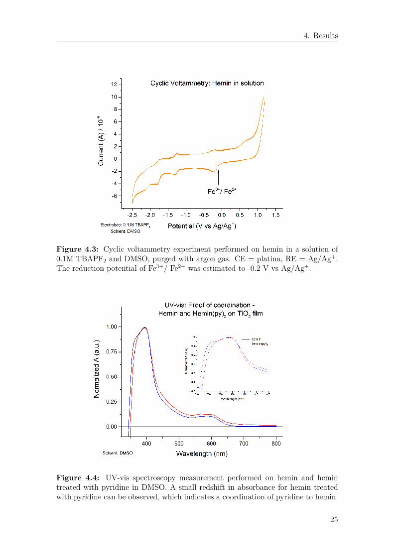
4.1.1 Spectroscopic and electrochemical properties of HeminThe reduction potential of hemin on TiO2 was initially investigated on a TiO2 filmin a DMSO solvent with 0.1 M TBAPF6 as electrolyte. However, due to complica-
23

4. Results
Figure 4.2: SEM images produced with secondary electrons of TiO2, SnO2 andmixed TiO2/SnO2 semiconductor films depicted from left to right respectively. Thesizes of the nanoparticles are all estimated in the range of 10-30 nm.
Table 4.1: Summary of elemental analysis performed with EDX at three differentpoints. The results are reported in atomic %.
O Ti SnSpectrum 1 69.71 % 27.67 % 2.62 %Spectrum 2 71.07 % 26.55 % 2.38 %Spectrum 3 70.48 % 27.00 % 2.52 %
tions with measuring the reduction potential of hemin on TiO2, no clear reductionpeak could be deduced and cyclic voltammetry measurements were performed insolution instead. The cyclic voltammetry measurement of hemin in DMSO and0.1M TBAPF6 seen in figure 4.3 is a previously unpublished result performed bymy supervisor Valeria Saavedra.
The formation of hemin(py)2 from hemin and pyridine was analyzed using UV-vis spectroscopy in a solution of DMSO with 0.1M TBAPF6 as electrolyte. Thesmall red shift in absorption for hemin treated with pyridine seen in figure 4.4 is anindication of formation of hemin(py)2 [25].
24
4. Results
Figure 4.3: Cyclic voltammetry experiment performed on hemin in a solution of0.1M TBAPF2 and DMSO, purged with argon gas. CE = platina, RE = Ag/Ag+.The reduction potential of Fe3+/ Fe2+ was estimated to -0.2 V vs Ag/Ag+.
Figure 4.4: UV-vis spectroscopy measurement performed on hemin and hemintreated with pyridine in DMSO. A small redshift in absorbance for hemin treatedwith pyridine can be observed, which indicates a coordination of pyridine to hemin.
25

4. Results
4.2 Conduction band mediated electron transfer
4.2.1 Photo induced band gap excitation in semiconduc-tors
To make sure the photolysis instrument is capable of photoinduced band gap excita-tion in both TiO2 and SnO2, photolysis experiments were performed on the semicon-ductors to visualize absorption from the conduction band. The broad, monotonicallyincreasing absorption seen between 400-1100 nm in figure 4.5a and 4.5b is consistentwith an increasing amount of electrons promoted to the conduction band [15].
(a) TiO2 (b) SnO2
Figure 4.5: Photolysis experiment of TiO2 and SnO2 displaying broad absorptionfrom the conduction band between 400 and 1100 nm.
4.2.2 Conduction band mediated transfer between semicon-ductor and electron acceptor
A second step towards a proof of principle for conduction band mediated electrontransfer is to induce band gap excitation in the semiconductor coupled to a re-duction of an electron acceptor. This experiment have been performed with twodifferent methods for band gap excitation; electric field and photo-excitation, usingspectroelectrochemistry and steady state photolysis respectively. The photolysisexperiment and spectroelectrochemistry results for hemin on TiO2 is displayed infigure 4.6 and 4.7. In these figures, a close resemblance of the two peaks located atapproximately 403 and 425 nm can be seen between the two experiments. In thephotolysis experiment however the peak at approximately 425 nm initially increasesrapidly, but starts a decrease after 30 seconds, unlike in the spectroelectrochem-istry experiment where the corresponding peak increase monotonically throughoutthe experiment (6 minutes). Furthermore, the isosbestic point located at 450 nmonly remains in the spectroelectrochemistry experiment, whereas in the photolysisexperiment the isosbestic point disappears in less than 2 minutes.
26

4. Results
Figure 4.6: Photolysis measurement depicting photo-induced reduction of heminon TiO2.
Figure 4.7: Spectroelectrochemistry measurement depicting reduction peaks ofhemin on TiO2 induced by stepwise increase in electric field potential (V).
27

4. Results
The same experiments were also performed on the SnO2 semiconductor with hemin(py)2as electron acceptor. The peaks located at 385 nm and 425 nm in the photolysisexperiment (figure 4.8) are also observed in the spectroelectrochemistry experiment(figure 4.9) at approximately the same wavelengths. These peaks are also corre-sponding well with the two peaks observed in the experiments with hemin on TiO2.The peak located at approximately 385 nm shows a monotonic decrease, and thepeak at 425 nm a monotonic increase in both the photolysis and spectroelectro-chemistry experiment. In addition, the isosbestic point also remain throughout theentire duration of the experiments.
Figure 4.8: Photolysis measurement depicting photo-induced reduction ofhemin(py)2 on SnO2.
4.3 Recombination study of semiconductor sys-tems
4.3.1 Excitation wavelengthThe pump wavelength was selected with an approximate optimal ratio of the dyeabsorption to the other components i.e. the electron acceptor. This was achievedby performing UV-vis spectra on D35CPDT and hemin on TiO2 and selecting thehighest absorption of D35CPDT to the lowest absorption of hemin, see figure 4.10.The same experiment with the SnO2 films was however not performed, as the effectof using a different semiconductor film likely only induce very small shifts in theabsorption spectra.
28

4. Results
Figure 4.9: Spectroelectrochemistry measurement depicting reduction peaks ofhemin(py)2 on SnO2 induced by a stepwise increase in electric field potential (V).
Figure 4.10: UV-vis spectra of D35CPDT, hemin and hemin(py)2 on TiO2. Theselected pump wavelength is indicated in the spectra by the black arrow at 520 nm.
29

4. Results
4.3.2 Probe wavelengthThe probe wavelength was selected to achieve minimal overlap between the dye andthe electron acceptor in order to avoid absorption not coupled to the recombinationprocess. This was possible by performing and comparing the UV-vis spectra of thedye in its oxidized state and the electron acceptors in their reduced state. Due totime restraints, the measurements could not be performed on the same semicon-ductor and solvent. The UV-vis spectrum of the oxidized D35CPDT was achievedon TiO2 in acetonitrile, the reduced hemin on TiO2 in DMSO, and the reducedhemin(py)2 on SnO2 in DMSO. The results of these spectra can be seen in figure4.11.
Figure 4.11: UV-vis spectra of the oxidized dye D35CPDT, and the reducedelectron acceptors hemin and hemin(py)2. The chosen probe wavelength is indicatedby a black arrow at 700 nm.
4.3.3 Quantification of photoinduced electron transfer rateusing transient absorption spectroscopy
4.3.3.1 The effect of solvents on electron recombination
Transient absorption spectroscopy measurements were performed with different sol-vents including both acetonitrile and DMSO, with and without addition of methanol.The results performed with D35CPDT on TiO2 is displayed in figure 4.12. The slow-est decay of the oxidized dye or rate of recombination, was observed for acetonitrilewithout methanol, followed by acetonitrile with methanol, and lastly DMSO witha significantly faster rate of recombination than both other solvents. The result
30

4. Results
for DMSO with methanol however was not included in figure 4.12 as it displayed anegative absorption which could not be explained. As a consequence the transientabsorption measurements with different semiconductor systems were performed inacetonitrile with methanol, to avoid an unknown process occurring in the sam-ple.
Figure 4.12: Transient absorption measurements of D35CPDT on TiO2 films inacetonitrile and DMSO with and without methanol.
The solvent’s effect on the rate of recombination was also investigated on the SnO2semiconductor with DMSO and acetonitrile with methanol. The rate of recombi-nation displayed in figure 4.13 for DMSO with methanol was significantly fasterthan the recombination rate for acetonitrile with methanol. In addition, the rate ofrecombination compared between TiO2 and SnO2 in figure 4.12 and 4.13 is muchfaster for SnO2.
4.3.3.2 The effect of semiconductor systems on electron recombination
Different semiconductor systems were investigated with transient absorption spec-troscopy in acetonitrile with methanol. The results are displayed in figure 4.14below. The slowest decay, is observed for the SnO2 semiconductor, followed bythe mixed TiO2/SnO2 and TiO2. In addition the semiconductors with hemin(py)2adhered to the surface, show a slower recombination than all other systems. Therate constants obtained from fitting all the transient absorption measurements aresummarized in table 4.2.
31

4. Results
Figure 4.13: Transient absorption measurements of D35CPDT on SnO2 films inDMSO and acetonitrile with methanol added to both solutions.
Table 4.2: Table of rate constants obtained from curve fitting with a biexponentialfunction. The parameters A1 and A2 have for convenience been converted into% to easier describe the amount of recombination occurring with each individualrecombination processes.
Sample Solvent A1(%)
A2(%)
K1(10−4)
K2(10−4)
Ktot(10−4)
D35CPDT - TiO2 DMSO 87 13 2.3 0.5 3.0D35CPDT - TiO2 DMSO/MeOH 83 17 3.2 1.4 5.7D35CPDT - SnO2 DMSO/MeOH 96 4 3.6 0.5 5.7D35CPDT - TiO2 MeCN 50 50 1.2 0.1 0.6D35CPDT - TiO2 MeCN/MeOH 60 40 0.8 0.1 0.6D35CPDT - SnO2 MeCN/MeOH 60 40 2.3 0.4 2.0D35CPDT - TiO2/SnO2 MeCN/MeOH 49 51 1.4 0.2 0.9D35CPDT - TiO2 -Hemin(py)2
MeCN/MeOH 54 46 1.0 0.1 0.6
D35CPDT - TiO2/SnO2 -Hemn(py)2 MeCN/MeOH 46 54 0.8 0.1 0.6
32

4. Results
Figure 4.14: Transient absorption measurements of D35CPDT on different semi-conductor systems with and without an electron acceptor. The slightly stepwisedecay observed for the green and orange curve, is an artifact attributed to poorsettings of the oscilloscope.
33

4. Results
34

5Discussion
5.1 Conduction band mediated electron transfer
The photolysis experiment on TiO2 and SnO2, seen in figure 4.5a and 4.5b, displaya broad absorption from 400 - 1100 nm which is consistent with electrons beingpromoted from the valence band to the conduction band[15]. This photolysis exper-iment, thus proves that band gap excitations can occur with the xenon lamp, andthe filters (transmittance between 260-400 nm).The conduction band mediated electron transfer was investigated using photolysisand spectroelectrochemistry as two complementary methods to each other. In figure4.6 the photolysis experiment of hemin on TiO2 show clear peaks at 403 and 425nm, which are consistent with literature data of Fe3+ and Fe2+ respectively [26]. Asimilar spectrum is also obtained for spectroelectrochemistry, see figure 4.7, in whichthe Fe3+ and Fe2+ are located at approximately the same wavelengths. However, onesignificant difference between the two methods is the disappearance of the isosbesticpoint at 450 nm after approximately 2 minutes in the photolysis experiment. Thisis contrary to the spectroelectrochemistry experiment where the isosbestic point re-main through the entire duration of the experiment (6 minutes). The disappearanceof the isosbestic point in combination with a decrease in Fe2+ observed in the pho-tolysis experiment suggests a formation of Fe+. The explanation as to why this onlyoccurs in the photolysis experiment is unclear, however the process by which thereduction of hemin occur is fundamentally different for the photolysis and spectro-electrochemistry experiments. In photolysis, no external electrons are supplied andthe reduction can thus only occur by electrons supplied from the conduction bandof the semiconductor. The spectroelectrochemistry method however, uses a counterelectrode to supply and transport the electrons through an external current to theworking electrode which generates an excess of electrons in the sample.Although spectroelectrochemistry is a complementary method to photolysis as itpromote electrons in the conduction band differently, the results gained from ana-lyzing porous semiconductor films may be difficult to interpret. According to someliterature [34], the porous semiconductor could allow molecules to diffuse through theporous semiconductor film, and accept electrons directly from the working electrodewithout necessarily utilizing the conduction band in the semiconductor. However,as the absorption peak for Fe2+ in the photolysis experiment, is consistent withboth literature, and spectroelectrochemistry and significantly larger than the autoreduction performed on of hemin under dark conditions (see figure A.1), there isstrong indication of an induced conduction band mediated electron transfer process
35

5. Discussion
for hemin on TiO2.In figure 4.8 and 4.9, the photolysis and spectroelectrochemistry results for hemin(py)2and SnO2 can be observed. There is a close resemblance between these results andthe results of hemin on TiO2. This is not too surprising as the coordination of pyri-dine to hemin and a slightly different semiconductor should theoretically only inducea small shift in absorption wavelength due to a changed electronegativity [35]. It istherefore relatively easy to identify the absorption peaks for Fe3+ and Fe2+ whichcan be approximated to 385 nm and 425 nm respectively for the photolysis spec-tra. With a monotonically increasing absorption peak of Fe2+ in both photolysisand spectroelectrochemistry, and no disappearing isosbestic points, formation ofFe+ seems unlikely. With the same argument as previously, the reduction peakscorresponding well with both methods and literature seems to indicate a conductionband mediated electron transfer process.
5.2 The effect of solvents on recombinationAs a small part of this thesis, the effect of solvents on the electron recombinationwas investigated. The results observed in figure 4.12, display a clear difference inrecombination rate for the different solvents. In DMSO the rate of recombinationis significantly faster than acetonitrile, which is observed both with and withoutaddition of methanol on TiO2 and SnO2 (see figure 4.13). Another interesting ob-servation of the study of solvents, is the effect of methanol, which was initially addeddue to its known ability to donate electrons (hole scavenger). Methanol was theo-rized to decrease the rate of recombination, as the donated electrons fill up the holesin the system and thereby making recombination difficult. However, the effect ofadding methanol, displays the opposite behaviour and recombination occur faster.Without investigating the mechanism for recombination, it is difficult to draw anyconclusions as to why this occurs.
5.3 The effect of semiconductor assemblies on re-combination
Due to the strong effect on electron recombination by using different solvents, thesemiconductor assemblies have been evaluated in the same solvent. In the measure-ments performed in the solvent acetonitrile with methanol, see figure 4.14 and table4.2, several interesting observations can be made. Firstly, the SnO2 recombinationis observed to be faster than for TiO2, despite its lower thermodynamical drivingforce. This behaviour is also supported in literature [36] and could potentially beexplained by a relatively lower electron injection efficiency, and faster electron mo-bility [37]. It is however, worth mentioning that a high electron mobility may onlyhave a negative impact on the recombination rate in a system lacking an electronacceptor, as once electrons transferred to the electron acceptor cannot easily recom-bine.Another interesting observation is the rate of recombination for the mixed TiO2/SnO2
36

5. Discussion
semiconductor system, which is slower than SnO2 and similar to or possibly fasterthan TiO2. By using the EDX results in table 4.1, the composition of the semicon-ductor film, can be estimated to approximately 90 atomic% TiO2 and 10 atomic%SnO2. The close correlation between the concentration of TiO2 and the electron re-combination rate observed in figure 4.14, seems to suggest a very small or negligiblecontribution of using TiO2 in combination with SnO2 for this system and concentra-tion. It should be stressed however, that since no experiments have been performedwith different concentrations, no general conclusions concerning the effect of mixingTiO2 and SnO2 can be made. One explanation for the measurement could be thatelectrons are not efficiently transferred between the TiO2 and SnO2, thus formingan average of two independent recombination processes. This explanation, howeverseems unlikely as the recombination occurs over a relatively long time interval, andelectron transfer between the semiconductors should be possible. An alternativeexplanation could be that the effect of cascade electron transfer only show a verysmall incremental effect on the electron injection efficiency compared to direct elec-tron transfer. Regardless, these theories are impossible to confirm without moreexperimental data on different concentrations. However, one observation that canbe made is that, long lived charge separated states induced by a physical barrier,see figure 2.8 do not seem to form in a significant concentration.The results of TiO2 and the mixed TiO2/SnO2 semiconductor system with the elec-tron acceptor hemin(py)2, display a considerably slower recombination than therecombination observed without an electron acceptor. This behaviour can relativelyeasily be explained by considering the electron transfer from the electron acceptorto the dye as very slow, and thereby decreasing the rate of recombination. The ef-fect of slower recombination however, is most prominent in the mid region of figure4.14 (between 200-1300 microseconds) and after approximately 2 milliseconds ap-proaches the same concentration as the other semiconductor systems. This can alsobe observed from the coefficients in table 4.2 where a lower value of A1 is obtainedfor both measurements performed with hemin(py)2. As the comparably lower rateof recombination for systems with hemin(py)2 is time dependent, the advantage ofusing an electron acceptor distributed throughout the semiconductor film is alsodependent on the catalytic rate of reaction in the solar fuel device. If the bulk of thecatalytic reaction is achieved in the late region of figure 4.14 (for instance 2 millisec-onds or later), the advantage may be small, whereas if most of the reaction occursin the mid region (between 200-1300 microseconds) the effect may a significant im-provement. One possible way of implementing these results obtained from studyingthe electron acceptors, could be to use catalysts incorporated in the semiconductorfilm to minimize the recombination.
37

5. Discussion
38

6Conclusion
This thesis have successfully shown proof of conduction band mediated electrontransfer for hemin on TiO2 and hemin(py)2 on SnO2 through experiments withsteady state photolysis and spectroelectrochemistry. A decreased rate of recom-bination with mixed TiO2/SnO2 semiconductors, was not observed in transientabsorption measurements, but further experiments on different concentrations arenecessary in order to conclude a general effect from cascade electron transfer. Inaddition, the transient absorption measurements performed on TiO2 and mixedTiO2/SnO2 with hemin(py)2 in acetonitrile with methanol displayed a longer livedcharge separated state. This effect was especially apparent in the range of 200 to1300 microseconds, and could potentially have significant implications for designingfuture solar fuel devices.
6.1 Future workThis thesis was mainly been aimed towards investigating the fundamental behaviourof mixed TiO2/SnO2 semiconductor films with regards to electron recombination.However, one interesting aspect that was only briefly discussed was long livedcharged separated states created by a physical barrier, see figure 2.8. This idea couldbe interesting to try out with screen printing or similar methods for strategic place-ment of the components of the solar fuel assembly. A requirement for this would beto create a SnO2 paste of appropriate nanoparticle size and viscosity. Additionally,a study on the effect of concentrations in mixed TiO2/SnO2 semiconductors couldbe interesting to investigate to determine if a cascade electron transfer mechanismcould be an improvement for solar fuel devices.
39

6. Conclusion
40

Bibliography
[1] Lewis NS, Crabtree G. Basic research needs for solar energy utilization: reportof the basic energy sciences workshop on solar energy utilization, April 18-21,2005. 2005;.
[2] Hammarström L. Accumulative charge separation for solar fuels production:Coupling light-induced single electron transfer to multielectron catalysis. Ac-counts of chemical research. 2015;48(3):840–850.
[3] Corma A, Garcia H. Photocatalytic reduction of CO 2 for fuel production:Possibilities and challenges. Journal of Catalysis. 2013;308:168–175.
[4] Sheehan SW, Thomsen JM, Hintermair U, Crabtree RH, Brudvig GW, Schmut-tenmaer CA. A molecular catalyst for water oxidation that binds to metal oxidesurfaces. Nature communications. 2015;6.
[5] Blankenship RE, Tiede DM, Barber J, Brudvig GW, Fleming G, Ghirardi M,et al. Comparing photosynthetic and photovoltaic efficiencies and recognizingthe potential for improvement. science. 2011;332(6031):805–809.
[6] Corma A, Garcia H. Photocatalytic reduction of CO 2 for fuel production:Possibilities and challenges. Journal of Catalysis. 2013;308:168–175.
[7] Shen J, Kortlever R, Kas R, Birdja YY, Diaz-Morales O, Kwon Y, et al. Elec-trocatalytic reduction of carbon dioxide to carbon monoxide and methane atan immobilized cobalt protoporphyrin. Nature communications. 2015;6.
[8] Evans RC, Douglas P, Burrow HD. Applied photochemistry. Springer; 2013.[9] Ceroni P. The exploration of supramolecular systems and nanostructures by
photochemical techniques. vol. 78. Springer Science & Business Media; 2011.[10] Lakowicz JR. Principles of fluorescence spectroscopy. 3rd ed. New York:
Springer; 2006.[11] Berera R, van Grondelle R, Kennis JT. Ultrafast transient absorption spec-
troscopy: principles and application to photosynthetic systems. Photosynthesisresearch. 2009;101(2-3):105–118.
[12] Saavedra Becerril V. Studies of Charge Separation in Molecular and Molecular-Inorganic Materials Assemblies for Solar Energy Conversion. 2015;.
[13] Kittel C. Introduction to solid state physics. Wiley; 2005.[14] Bard AJ, Faulkner LR. Electrochemical methods: fundamentals and applica-
tions. 2nd ed. New York: Wiley; 2001.[15] Serpone N, Lawless D, Khairutdinov R. Size effects on the photophysical prop-
erties of colloidal anatase TiO2 particles: size quantization versus direct tran-sitions in this indirect semiconductor? The journal of Physical Chemistry.1995;99(45):16646–16654.
41

Bibliography
[16] Nazeeruddin MK, Baranoff E, Grätzel M. Dye-sensitized solar cells: a briefoverview. Solar Energy. 2011;85(6):1172–1178.
[17] Vinodgopal K, Bedja I, Kamat PV. Nanostructured semiconductor films forphotocatalysis. Photoelectrochemical behavior of SnO2/TiO2 composite sys-tems and its role in photocatalytic degradation of a textile azo dye. Chemistryof materials. 1996;8(8):2180–2187.
[18] Willkomm J, Orchard KL, Reynal A, Pastor E, Durrant JR, Reisner E. Dye-sensitised semiconductors modified with molecular catalysts for light-driven H2 production. Chemical Society Reviews. 2016;45(1):9–23.
[19] Bai Y, Mora-Seró I, De Angelis F, Bisquert J, Wang P. Titanium dioxide nano-materials for photovoltaic applications. Chemical reviews. 2014;114(19):10095–10130.
[20] Nasr C, Kamat PV, Hotchandani S. Photoelectrochemistry of composite semi-conductor thin films. Photosensitization of the SnO2/TiO2 coupled systemwith a ruthenium polypyridyl complex. The Journal of Physical ChemistryB. 1998;102(49):10047–10056.
[21] Kochanski E, service) SO, (e-book collection) SA. Photoprocesses in TransitionMetal Complexes, Biosystems and Other Molecules. Experiment and Theory.vol. 376. Dordrecht: Springer Netherlands; 1992.
[22] Fukuzumi S, Ohkubo K, Suenobu T. Long-lived charge separation andapplications in artificial photosynthesis. Accounts of chemical research.2014;47(5):1455–1464.
[23] Miller J, Calcaterra L, Closs G. Intramolecular long-distance electron transferin radical anions. The effects of free energy and solvent on the reaction rates.Journal of the American Chemical Society. 1984;106(10):3047–3049.
[24] Tian H, Soto A, Xu B, Sun L, Hagfeldt A, Fabregat-Santiago F, et al. Effectof the chromophores structures on the performance of solid-state dye sensitizedsolar cells. Nano. 2014;9(05):1440005.
[25] Staniszewski A, Morris AJ, Ito T, Meyer GJ. Conduction band mediated elec-tron transfer across nanocrystalline TiO2 surfaces. The Journal of PhysicalChemistry B. 2007;111(24):6822–6828.
[26] Ito T. Reactions of Heme Catalysts at Nanocrystalline TiO2 Thin Film Inter-faces with Organohalide Pollutants. Johns Hopkins University; 2007.
[27] Di Valentin C, Fittipaldi D. Hole Scavenging by Organic Adsorbates on theTiO2 Surface: A DFT Model Study. The journal of physical chemistry letters.2013;4(11):1901–1906.
[28] Harvey D. Modern analytical chemistry. vol. 798. McGraw-Hill New York;2000.
[29] Gallot S, Thomas O. Fast and easy interpretation of a set of absorption spectra:theory and qualitative applications for UV examination of waters and wastew-aters. Fresenius’ journal of analytical chemistry. 1993;346(10-11):976–983.
[30] Khursheed, (e-book collection) E. Scanning Electron Microscope Optics andSpectrometers. Hackensack: World Scientific Publishing Company, Incorpo-rated; 2010;2011;.
[31] Alibabaei L, Sherman BD, Norris MR, Brennaman MK, Meyer TJ. Visi-ble photoelectrochemical water splitting into H2 and O2 in a dye-sensitized
42

Bibliography
photoelectrosynthesis cell. Proceedings of the National Academy of Sciences.2015;112(19):5899–5902.
[32] Felter K. Charge separation in organic semiconductors. Delft University ofTechnology. the Netherlands; 2015.
[33] Ardo S, Achey D, Morris AJ, Abrahamsson M, Meyer GJ. Non-Nernstian two-electron transfer photocatalysis at metalloporphyrin–TiO2 interfaces. Journalof the American Chemical Society. 2011;133(41):16572–16580.
[34] Wang Q, Zakeeruddin SM, Nazeeruddin MK, Humphry-Baker R, Grätzel M.Molecular wiring of nanocrystals: NCS-enhanced cross-surface charge transferin self-assembled Ru-complex monolayer on mesoscopic oxide films. Journal ofthe American Chemical Society. 2006;128(13):4446–4452.
[35] Akers JW, Gensic AP, Nalliah RE. Solvent effects on the electronic transi-tion energies of porphyrins in binary solvent mixtures. In: Proceedings of theIndiana Academy of Science. vol. 110; 2001. p. 28–34.
[36] Green AN, Palomares E, Haque SA, Kroon JM, Durrant JR. Charge trans-port versus recombination in dye-sensitized solar cells employing nanocrys-talline TiO2 and SnO2 films. The Journal of Physical Chemistry B.2005;109(25):12525–12533.
[37] Tiwana P, Docampo P, Johnston MB, Snaith HJ, Herz LM. Electron mobilityand injection dynamics in mesoporous ZnO, SnO2, and TiO2 films used indye-sensitized solar cells. ACS nano. 2011;5(6):5158–5166.
43

Bibliography
44

AAppendix 1
Figure A.1: Autoreduction of hemin on TiO2 performed in DMSO with 0,1MTBAPF6 in a dark room.
I

A. Appendix 1
Figure A.2: Autoreduction of hemin(py)2 on TiO2 performed in DMSO with 0,1MTBAPF6 in a dark room.
A.1 EDX locations on SnO2/TiO2 film
Figure A.3: SEM image of the location of spectrum 1.
II

A. Appendix 1
Figure A.4: SEM image of the location of spectrum 2.
Figure A.5: SEM image of the location of spectrum 3.
III