electron band structure in solids - home | university of ... dirac funcon density of states x...
TRANSCRIPT
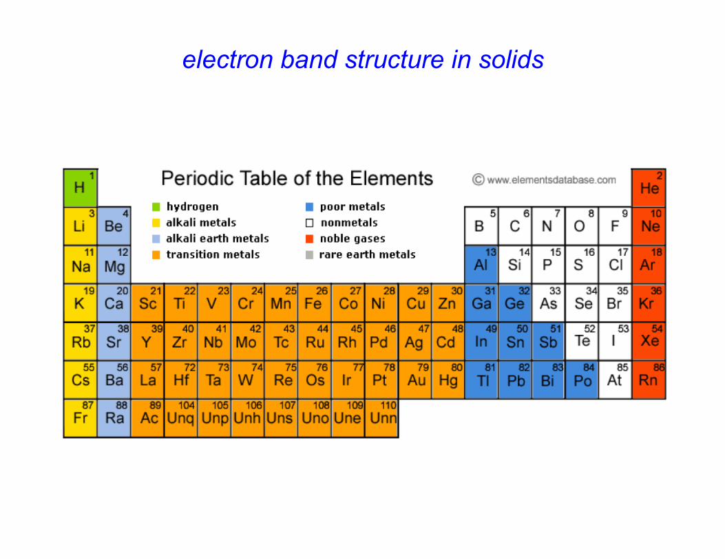
electron band structure in solids

formation of bands
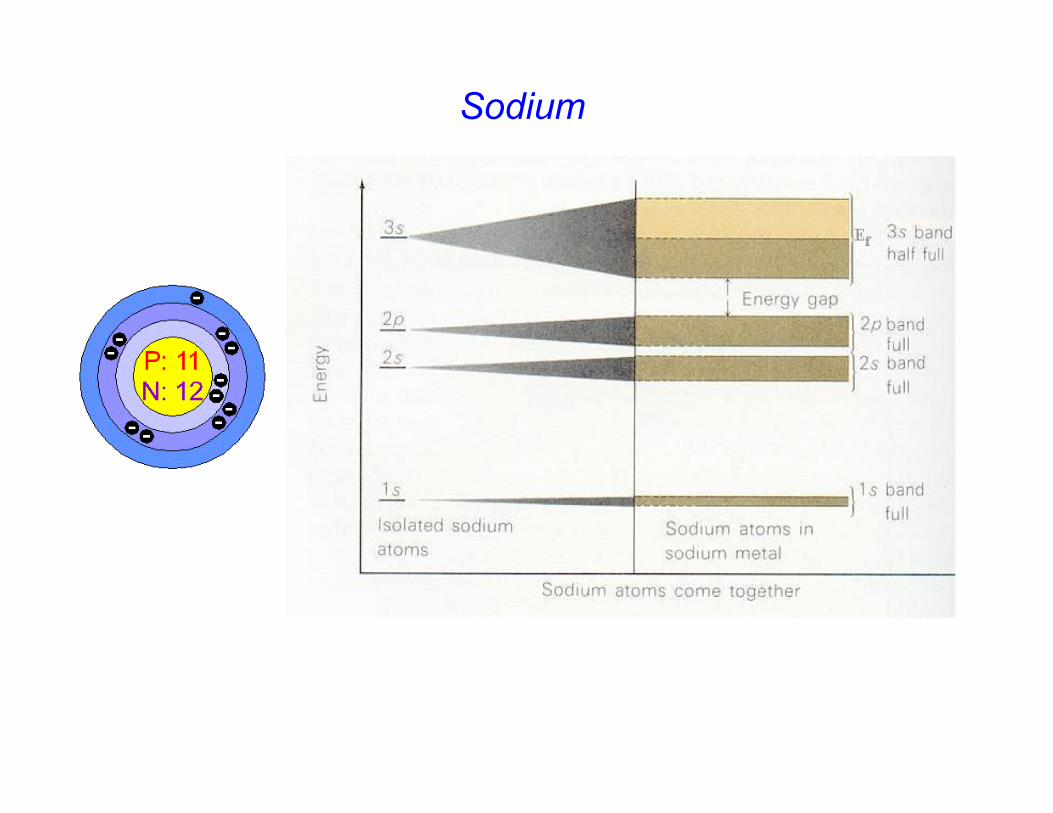
Sodium
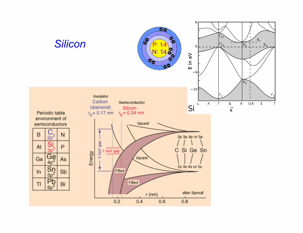
Silicon
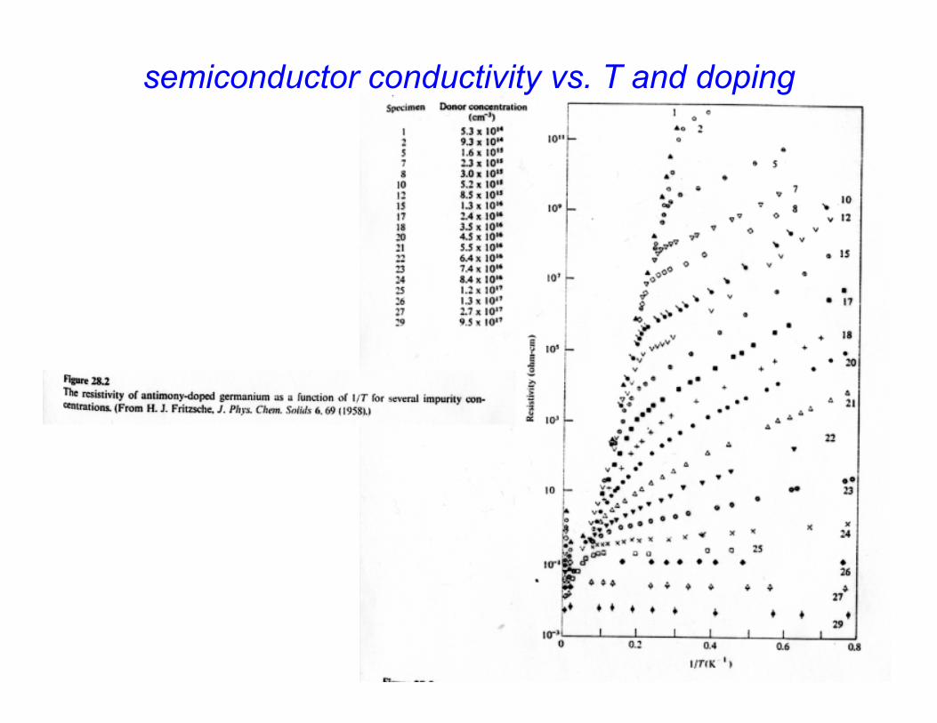
semiconductor conductivity vs. T and doping

valence and conduction band structure
ndoping:electronsaremajority
carriers
nodoping
pdoping:Holesaremajority
carriers
Fermi‐Dirac
func9on
densityof
states
Fermi‐Dirac
func9on
densityof
statesX
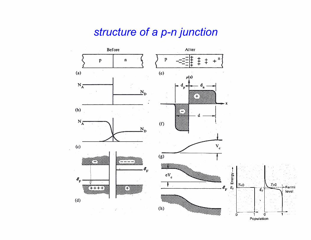
structure of a p-n junction
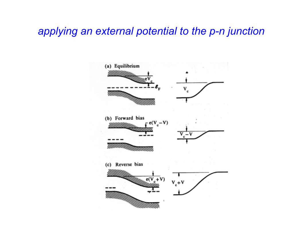
applying an external potential to the p-n junction
+++++++++
|||||||||||
+++++++++
|||||||||||
+ ‐
‐ +
|||||||||||
+++++++++
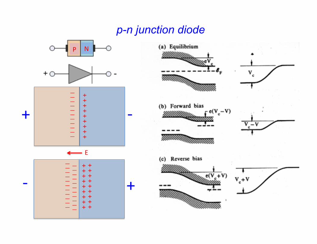
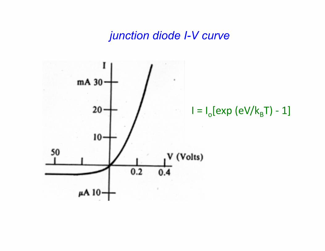
p-n junction diode
E
NP

I=Io[exp(eV/kBT)‐1]
junction diode I-V curve
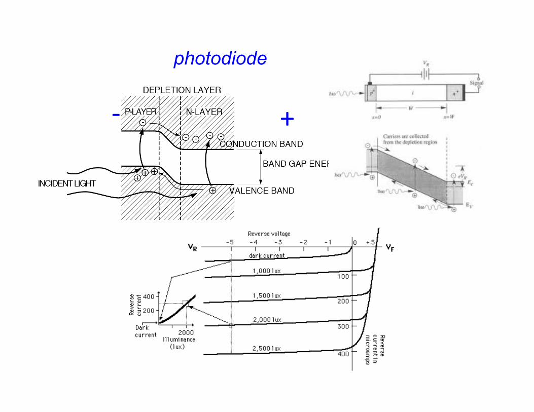
photodiode
‐ +

current(A)/op>calpower(W)=A/W=λ(nm)xQE}/1240
QE=1
photodiode response
current=e[ne]=e[QE(np)]=e[QE(op>calpower/{hc/λ})]

Vout(V)={op>calpower(W)xλ(nm)xQExRf(Ω)}/1240
photodiode and current amplifier
Vout(V)=A/WxRf(Ω)
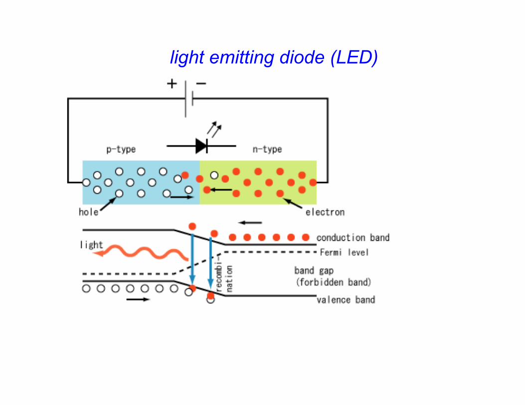
light emitting diode (LED)
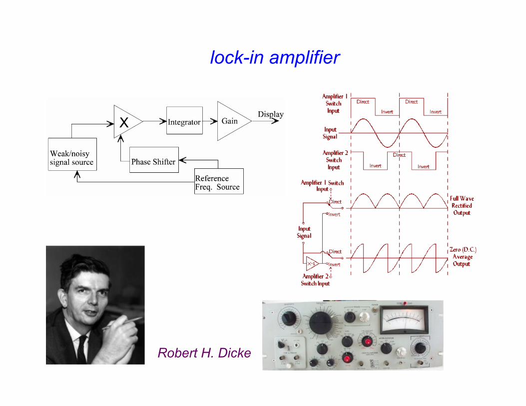
lock-in amplifier
Robert H. Dicke

the triode
V+
load line (slope = R = 50KΩ)
R 50KΩ
L. De Forest (1907)
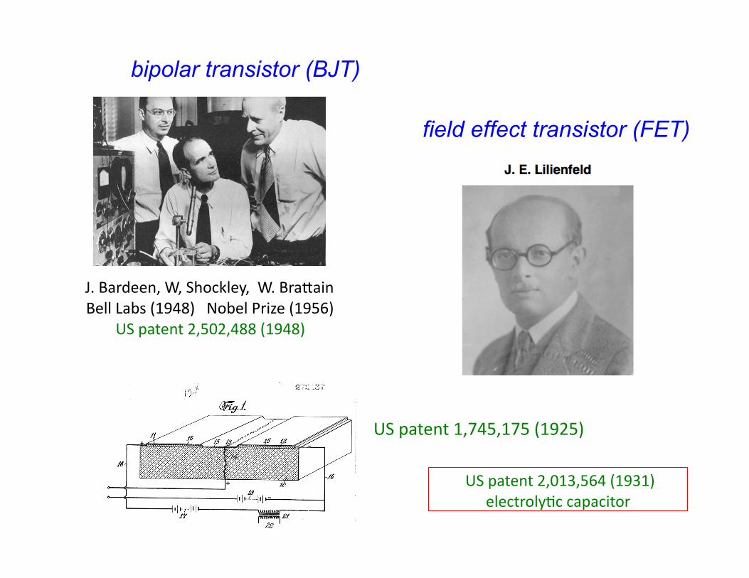
bipolar transistor (BJT)
J.Bardeen,W,Shockley,W.BraSainBellLabs(1948)NobelPrize(1956)
field effect transistor (FET)
USpatent1,745,175(1925)
USpatent2,502,488(1948)
USpatent2,013,564(1931)electroly>ccapacitor

bipolar junction transistor (BJT)
‐
+
‐+
‐
+
+++++++++
+++++‐‐‐‐‐‐‐
‐‐‐‐‐‐‐‐‐‐‐
+++++||||||||
||||||||
+++++
||||||||
+++++
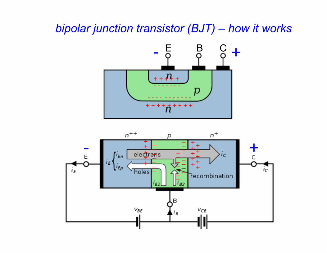
bipolar junction transistor (BJT) – how it works
E B C ‐ +
‐ +

+++++++++
|||||||||||
+++++++++
|||||||||||
+ ‐
‐ +
|||||||||||
+++++++++
p-n junction diode
E
NP
I=Io[exp(eV/kBT)‐1]
junction diode I-V curve
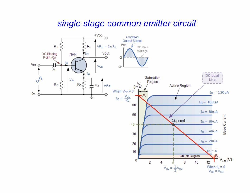
single stage common emitter circuit
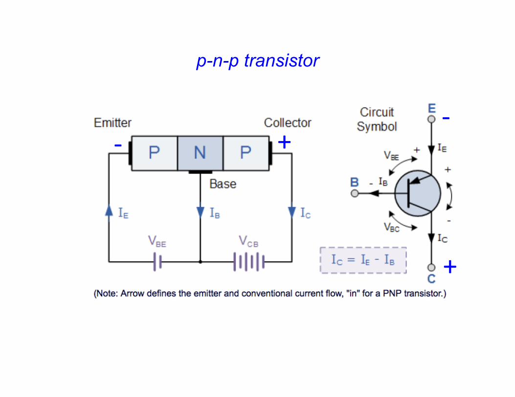
p-n-p transistor
‐
+
‐+

complementary transistors – control + and - voltage
‐
+

junction field effect transistor (JFET)
‐
+

circuit biasing n-channel JFET and circuit symbols
‐ +
‐ +