electromechanical considerations in developing low-voltage rf mems...
TRANSCRIPT

IEEE TRANSACTIONS ON MICROWAVE THEORY AND TECHNIQUES, VOL. 51, NO. 1, JANUARY 2003 259
Electromechanical Considerations in DevelopingLow-Voltage RF MEMS Switches
Dimitrios Peroulis, Member, IEEE, Sergio P. Pacheco, Member, IEEE, Kamal Sarabandi, Fellow, IEEE, andLinda P. B. Katehi, Fellow, IEEE
Abstract—This paper reports on the design, fabrication, andtesting of a low-actuation voltage Microelectromechanical systems(MEMS) switch for high-frequency applications. The mechanicaldesign of low spring-constant folded-suspension beams is pre-sented first, and switches using these beams are demonstratedwith measured actuation voltages of as low as 6 V. Furthermore,common nonidealities such as residual in-plane and gradientstress, as well as down-state stiction problems are addressed, andpossible solutions are discussed. Finally, both experimental andtheoretical data for the dynamic behavior of these devices arepresented. The results of this paper clearly underline the needof an integrated design approach for the development of ultralow-voltage RF MEMS switches.
Index Terms—Low actuation voltage, microelectromechanicalsystems (MEMS) switches, residual stress, spring constant,switching speed, top-electrode switches.
I. INTRODUCTION
M ICROMACHINING and microelectromechanical sys-tems (MEMS) are among the most promising enabling
technologies for developing low-power low-cost miniaturizedRF components for high-frequency applications. Several uni-versities and companies have developed RF MEMS switches[1]–[8] in the last decade that can be primarily classified as:1) series or shunt; 2) fixed–fixed membranes or cantileverbeams; and 3) capacitive or metal-to-metal contact type [9].The main driving force behind this major research effort isthe outstanding demonstrated RF performance of the MEMSswitches from dc to 100 GHz compared to p-i-n diodes orFET transistors. Furthermore, electrostatically driven switchesrequire only a few microwatts of dc power compared to severalmilliwatts that their solid-state counterparts dissipate. It isfor this reason, as well as for the simplicity of their biasing
Manuscript received April 22, 2002. This work was supported by the Systemon a Chip/Jet Propulsion Laboratory under the Center for Integrated Space Mi-crosystems Project and by the Department of Defense Research and Engineeringunder the Multidisciplinary University Research Initiative on “Low Power Elec-tronics” and “Multifunctional Adaptive Radio, Radar and Sensors” programs.
D. Peroulis and K. Sarabandi are with the Radiation Laboratory,Electrical Engineering and Computer Science Department, The Universityof Michigan at Ann Arbor, Ann Arbor, MI 48109-2122 USA (e-mail:[email protected]).
S. P. Pacheco was with the Radiation Laboratory, Electrical Engineeringand Computer Science Department, The University of Michigan at Ann Arbor,Ann Arbor, MI 48109-2122 USA. He is now with Digital DNA Laboratories,Motorola, Tempe, AZ 85284 USA.
L. P. B. Katehi was with the Radiation Laboratory, Electrical Engineeringand Computer Science Department, The University of Michigan at Ann Arbor,Ann Arbor, MI 48109-2122 USA. She is now with the College of Engineering,Purdue University, West Lafayette, IN 47907 USA.
Digital Object Identifier 10.1109/TMTT.2002.806514
networks, that most of the developed switches are electrostaticin nature.
These studies, however, have only limited their focus onthe RF performance of MEMS switches and have providedlittle information on several important phenomena directlyrelated to the inherent electromechanical characteristics ofthese structures. Their sheer interdisciplinary nature imposesa very tight coupling between the electrical and mechanicaldomains. For instance, thin-film residual stress and viscousdamping may have a far greater influence on the performanceof the device than intuitively anticipated. Moreover, the vastmajority of the switches in the literature typically requirea pull-in and hold-down voltage of 40–100 and 15–30 V,respectively. Whereas no difficulty exists in achieving theseranges in a typical laboratory environment, they may be quitechallenging for handheld mobile phones, automotive vehicles,and similar wireless devices that rely on low-voltage powersupplies. In addition, Goldsmithet al. [16] have shown that thelifetime of capacitive switches strongly depends on the appliedactuation voltage. In particular, for capacitance switches, theyexperimentally observed a lifetime improvement of a decadefor every 5–7-V drop on the switch pull-in voltage. Conse-quently, reducing the actuation voltage of MEMS switchesmay not only broaden the range of their possible applications,but also significantly enhance their performance. It wouldseem, therefore, that further investigations are needed in orderto provide the MEMS engineer with complete and accurateinformation on the design and operation of these devices.
It is the purpose of this paper to present the results of our in-vestigation on these issues. First, in Section II, we focus on thedesign of the low spring-constant beams that support the mainswitch structure. We also demonstrate a number of designs thatresulted in switches with pull-in voltages of as low as 6 V. Sec-tion III discusses the effects of residual axial and gradient stresson the device performance and shows how minor design andfabrication details may have a significant impact on the finalstructure. Section IV concludes our study by presenting exper-imental and theoretical results on the dynamic behavior of thelow-voltage MEMS switch.
II. SPRING CONSTANT AND ACTUATION VOLTAGE
A. Design
The mechanical design of most electrostatically basedswitches starts with considering the required dc actuationvoltage. Equation (1) presents a widely cited formula (e.g., [8])
0018-9480/03$17.00 © 2003 IEEE

260 IEEE TRANSACTIONS ON MICROWAVE THEORY AND TECHNIQUES, VOL. 51, NO. 1, JANUARY 2003
Fig. 1. SEM picture of the proposed low-voltage capacitive shunt switch overa CPW line.
for calculating the pull-in voltage of fixed-fixed beams or airbridges as follows:
(1)
is the equivalent spring constant of the moving structure inthe direction of desired motion (typically the-direction), isthe gap between the switch and the actuation electrode,isthe free-space permittivity, and is the switch area where theelectrostatic force is applied. Equation (1) implies that there areseveral ways that may decrease the required actuation voltage.For instance, reducing can significantly lower the pull-involtage. Although this solution can be partly applied to low-frequency applications (10 GHz), it will adversely affect thehigh-frequency off-state switch performance by compromisingthe switch isolation (for a series switch) or insertion loss (for ashunt switch). A second approach in lowering the pull-in voltagewould be to increase the actuation area. This area, however,has to stay within reasonable limits, primarily imposed by ourdesire for miniaturized circuits. The third alternative, which of-fers the maximum design flexibility for a low-to-moderate ac-tuation voltage, is to lower the switch spring constant, hence,designing a compliant switch.
Fig. 1 shows an SEM picture of our proposed switch in acoplanar waveguide (CPW) configuration. The switch consistsof three movable metallic plates, one over each conductor of theCPW line. These plates are connected together with three shortbeams (connecting beams) and the whole structure is connectedto the substrate at four points (anchors) through four beams.Due to their shape, we will call these beams serpentine springsor folded-suspension beams. The switch is typically suspended3–4 m above the CPW line and is electrostatically actuatedwhen a dc voltage is applied between the switch and the CPWground planes.
B. Fabrication
The fabrication process is fairly simple, requires only fourmasks, and is described in detail in [10]. The CPW line is typ-
ically made of Ti/Au (500/9000 ) and is defined first througha liftoff process. A plasma-enhanced chemical vapor deposition(PECVD) of approximately 1400–2000Si N follows. Sincethe switch is made of metal (typically Ni), this dielectric layer isprimarily needed during the actuation stage to prevent a direct dccontact between the switch and CPW line. Therefore, a positivephotoresist intended to protect the SiN underneath the switchis deposited with a normal lithography and the remaining dielec-tric layer is etched through a reactive ion etching (RIE) process.After the photoresist removal, the sacrificial layer (polyimide orphotoresist) is deposited and the switch anchor points are pho-tolithographically defined. Afterwards, a seed layer (typicallyTi/Ni 2000/500 ), is deposited, patterned, and electroplated.The last step is the removal of the sacrificial layer and the su-percritical CO drying of the structure.
C. Spring Design
Since the mathematical details of the electrostatic actuation[including (1)] have been extensively analyzed in the past [17],[18], we will just briefly describe the basic principle here. Whenno dc bias is applied, the switch presents a very small shunt ca-pacitance (typically in the order of 30–50 fF) between the centerconductor and ground planes. This is called the up or off stateand the RF signal can propagate with minimal loss (typicallywith 0.1 dB at -band). On the other hand, if the applied biasexceeds the actuation voltage, the switch collapses on the di-electric layer underneath, resulting in a significant shunt capac-itance, which is equivalent to an RF short circuit. This is calledthe down or on state and virtually all the incident RF power isreflected back to the source.
As was previously mentioned, the switch of Fig. 1 is con-nected to the substrate through four serpentine springs that areused to substantially lower the switch spring constant. Ifisthe -directed spring constant for each one of the springs, thetotal switch spring constant is given by
(2)
Compared to simple cantilever beams of equal total length,these springs have the additional advantage of occupyingconsiderable less space, but they also show higher springconstant. As will be shown, however, adding more meanderscan significantly lower it without excessively increasing therequired space. In the following, we calculate the springconstant of an -section meander [see Fig. 2(a)] when a virtualforce is applied at its free end. An analytical solution for asimilar folded meander has been obtained by Fedder [19] andour analysis is based on his study.
Each meander of the whole spring is defined as the set offour beams: two primary beams of lengthand two secondarybeams of length. Therefore, an -meander spring has 2pri-mary beams and 2 secondary beams. The switch shown inFig. 1, for instance, has a single-section meander ( ) with
m and m. All the necessary dimensions andmaterial constants for our switch are given in Table I. For the an-alytical calculation, it is assumed that all six degrees of freedomof the anchor point [point A in Fig. 2(a)] are fixed. Moreover,the guided-end boundary conditions are applied for the free-end
PEROULISet al.: ELECTROMECHANICAL CONSIDERATIONS IN DEVELOPING LOW-VOLTAGE RF MEMS SWITCHES 261
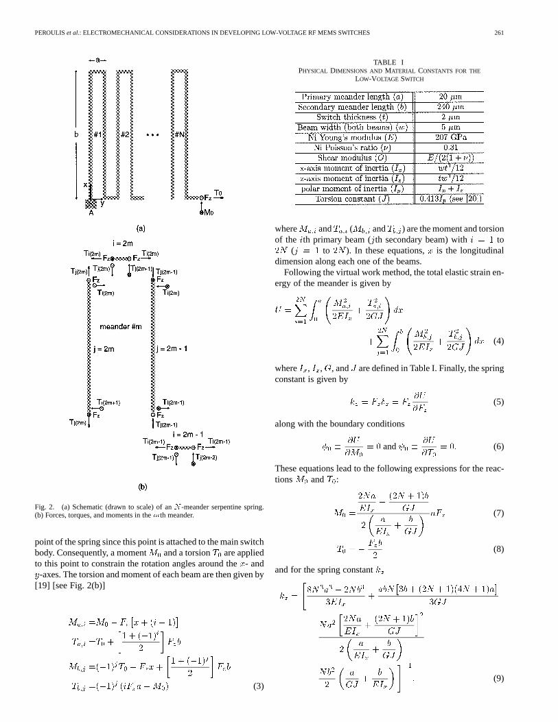
Fig. 2. (a) Schematic (drawn to scale) of anN -meander serpentine spring.(b) Forces, torques, and moments in themth meander.
point of the spring since this point is attached to the main switchbody. Consequently, a moment and a torsion are appliedto this point to constrain the rotation angles around the- and-axes. The torsion and moment of each beam are then given by
[19] [see Fig. 2(b)]
(3)
TABLE IPHYSICAL DIMENSIONS AND MATERIAL CONSTANTS FOR THE
LOW-VOLTAGE SWITCH
where and ( and ) are the moment and torsionof the th primary beam (th secondary beam) with to
( to ). In these equations, is the longitudinaldimension along each one of the beams.
Following the virtual work method, the total elastic strain en-ergy of the meander is given by
(4)
where , , , and are defined in Table I. Finally, the springconstant is given by
(5)
along with the boundary conditions
and (6)
These equations lead to the following expressions for the reac-tions and :
(7)
(8)
and for the spring constant
(9)

262 IEEE TRANSACTIONS ON MICROWAVE THEORY AND TECHNIQUES, VOL. 51, NO. 1, JANUARY 2003
Fig. 3. Analytically computed and FEM simulated results of thez-directedspring constant of anN -section meander.
Although (9) is lengthy, it is written in an intuitive way thatmay facilitate the design of these meanders or similar beams.The first two terms of the denominator represent the percentageof the spring constant that is due to beam bending (first term)and twisting (second term). In other words, these terms dependsolely on the meander geometry and the ability of the beam ma-terial to bend and twist. The last two terms of the denominatorare due to the boundary conditions of the meander moving endand correspond to its inability to rotate around the- and -axes.These two terms may have comparable magnitude to the firsttwo and considerably increase the switch spring constant.
Equation (9) was verified by a commercially availablefinite-element method (FEM) code [21]. The dimensions ofTable I were input in the code and several linear simulationswere performed for springs with 1–5 meanders. For eachsimulation, a concentrated-directed force of Nwas applied at the tip of the spring along with the necessaryguided-end boundary conditions. The resulting deflectionwas then computed and the FEM spring constant was extractedas . Excellent agreement between theanalytically and numerically computed spring constants isobserved in Fig. 3, which graphically presents the two springconstants as a function of the number of the meanders. Thisgraph also illustrates that the serpentine spring constant isnot significantly reduced after including four or five meandersections. Hence, three or four meanders would be a goodcompromise between low spring-constant requirements andspace limitations.
D. Actuation Voltage Measurements
Five switch designs with 1–5 meanders in their folded sus-pensions were fabricated and measured. Except for the serpen-tine springs, all designs were identical and were fabricated onthe same wafer by the same fabrication process. For each de-sign, we measured the pull-in voltage using an HP 4275A mul-tifrequency LCR meter with an internal bias option. These mea-surements are presented in Table II, which also compares the ex-tracted switch spring constant from the measured pull-in voltage[based on (1)] with the corresponding theoretical results. Thetheoretical values have been calculated for a switch thickness of
m (because of over-plating in the fabricated switches)
TABLE IIACTUATION VOLTAGE MEASUREMENTS FORSEVERAL MEMS SWITCHES
Fig. 4. Measured dc switch capacitance as a function of the applied biasvoltage and number of meanders.
and an initial gap of m. The reason for this highergap is that, although the sacrificial layer thickness was 4m,the induced residual stress across the structure caused a slightout-of-plane deflection, which, on average, increased the totaldistance from the substrate to 5m. We will discuss stress is-sues in more detail in Section III. Fig. 4 also shows the measureddc capacitance of the switches as a function of the applied biasvoltage and the number of meanders.
These data reveal several discrepancies between the simulatedand measured results. The first dissimilarity is the fact thatthe measured pull-in voltages are 5–10 times higher than thetheoretically calculated ones. The second and most interestingone is related to the percentage of the spring-constant reductionas the number of meanders is increased. For example, whenthe number of meanders was increased from one to two,the experimentally extracted spring constant was decreasedby 46%, while the theoretical calculations predicted 53%.Although these results are in fair agreement, this is not thecase for switches with more meanders. The switches with fivemeanders, for instance, had 70% lower spring constant thanthe ones with four. According to (9), however, this numbershould be close to 30%. Fig. 5 graphically illustrates theseobservations for all cases. All these issues are due to thehigh intrinsic axial stress built into the Ni layer during thefabrication and are studied in Section III.
E. Stiction and Top Electrode Design
Although low spring constant is essential in obtaining low-voltage switches, preventing down-state stiction is equally

PEROULISet al.: ELECTROMECHANICAL CONSIDERATIONS IN DEVELOPING LOW-VOLTAGE RF MEMS SWITCHES 263
Fig. 5. Experimental and theoretical percentage change of the switch springconstant as the number of meanders is increased.
Fig. 6. Top electrode concept and fabrication process. (a) 2500�A of SiO aredeposited on top of the switch followed by a second sacrificial layer. (b) The topelectrode is electroplated in a low-stress Au solution. (c) The whole structure isreleased by etching the sacrificial layers followed by a standard supercriticaldrying process.
important. A low-voltage switch experiences a relatively weakrestoring force while in the down state, which may not besufficiently high to pull the switch up, particularly in humidor contaminated environments. This drawback of this familyof switches can be overcome by including top electrodes.Fig. 6 illustrates the idea of fabricating a metallic plate (topelectrode) above the switch. By applying a dc voltage betweenthis top electrode and switch, the switch can be pulled up fromthe down state, even if the restoring force is not sufficientlyhigh.
Fig. 7 shows an example of a four-meander switch with topelectrodes over the dc switch pads. There is no electrode sus-pended above the center conductor pad because such an elec-
Fig. 7. Four-meander switch with top electrodes. Each top electrodeis approximately 5–6-�m thick and is fabricated with a low-stress Auelectroplated process.
trode would significantly deteriorate the up-state switch capac-itance. These top electrodes are very stiff fixed–fixed plates(5–6- m-thick low-stress electroplated Au) with a spring con-stant higher than 2300 N/m. Any movement of these electrodeswould require voltages in excess of 250 V and, compared withthe switch, they can be considered as static plates. Additionally,they provide stabilization to the overall switch structure againstsevere mechanical shocks. Measured and theoretical results ofswitches with top electrodes and power measurements of thesame switches are reported in [22].
III. I NTRINSIC RESIDUAL STRESSISSUES
Although the previous analysis allows for a first estimateof the switch spring constant and pull-in voltage, it doesnot account for any intrinsic residual stress on the structure.Residual stress, however, is developed during the fabricationof most microstructures and typically presents most of themajor challenges in developing these devices. Under this stress,thin-film structures can experience undesirable deformations,which may be significant, particularly for high-aspect ratiostructures. Additionally, many MEMS switches must satisfyvery stringent requirements for reliable performance, includingbeing planar over the circuit underneath it. Any undesirablebuckling or curling may easily deteriorate the performance ofthe switch, or lead to the complete failure of the device. A lotof attention, therefore, has to be paid to residual stress and itseffects on compliant structures before any successful devicescan be developed.
When a thin film is deposited on a sacrificial layer at atemperature lower than its flow temperature, then intrinsicstresses develop in the film-sacrificial layer system [23]. Anumber of studies have been already performed to theoreticallyexplain the mechanisms of these stresses [24], [25] and toexperimentally measure their effects [26], [27]. Nonetheless, ingeneral, thin-film stress is complicated and heavily dependson the specifics of the fabrication process. There is alsovery little information for metallic microstructures built bythin-films depositions and effective ways that can control itsstress and/or its effects. This section illuminates the mostimportant stress-related challenges for developing low-voltageswitches.

264 IEEE TRANSACTIONS ON MICROWAVE THEORY AND TECHNIQUES, VOL. 51, NO. 1, JANUARY 2003
Fig. 8. Thin-film residual-stress approximation.
Fig. 9. Switches with considerable deflection as a result of a poorly designedfabrication process.
A. Gradient Residual Stress
A general uniaxial residual stress field in a thin film can berepresented as [26]
(10)
where is the film thickness and is the coor-dinate across the film thickness, with its origin at the mid-planeof the film. For a first-order approximation, the total stress canbe calculated as
(11)
This equation implies that the total stress can be expressed as asuperposition of the constant mean stress(positive or nega-tive depending on whether the film is in tension or compression)and a gradient stress about the mid-plane (see Fig. 8). The ef-fects of the gradient stress are analyzed in this subsection andthose of the mean stress in the following one.
It is widely known that residual gradient stress causes unde-sirable out-of-plane deformation. Fig. 9 shows two examples ofextremely warped switches. These switches were 4-m thickand the maximum deformation, defined as the distance betweenthe higher and lower switch points, was on average 30m.This deformation was recorded for switches 640-m long (notcounting the length of the meanders), but increased to 70–80mfor switches close to 1-mm long. This substantial deformationrenders both structures unusable because: 1) the required actua-tion voltage is much higher than the design value (80 V) and 2)the up-state switch RF capacitance is considerably higher than
Fig. 10. Simulated warped switch structure (by SUGAR). The maximumswitch deflection is approximately 23�m.
anticipated ( fF, instead of 50 fF). The sacrificialand seed layers that resulted in such a stress were the polyimideDuPont PI2545 and an evaporated Ti/Ni (1500/500-) layer, re-spectively. The switches were then electroplated in an Ni so-lution (Nickel Sulfamate, Barrett SN by Mac Dermid) with asteady current density of 4 mA/cmfor approximately 30 min.The induced stress with this fabrication process was repeatableover a period longer than six months.
This switch shape under residual gradient stress was also the-oretically validated using SUGAR.1 Fig. 10 shows the simu-lated switch shape, which agrees very well with the fabricatedswitches. The maximum gradient stress value in the softwarewas varied until the measured maximum deflection was ob-tained.
One way to alleviate this problem without increasing the actu-ation voltage is to selectively increase the switch thickness [28].In this technique, the main switch body thickness is increasedto 6–8 m, but the springs remain 2-m thick [see Fig. 11(a)].This process utilizes the following two electroplating steps:
Step 1) The switch and the springs are plated.Step 2) The switch main body is subsequently plated again
until it reaches a thickness of 6–8m.Due to some adhesion difficulties between the two plated struc-tures, the process was slightly changed by plating only a switchframe during the first step instead of the whole switch [seeFig. 11(b)]. This improvement resulted in a 98% yield.
The drawback of this technique, however, is that, although itlimits the switch warping to 1–3m and may prove useful forother types of MEMS devices, it also results in less conformalswitches with lower down-state capacitance than the originalswitches.
We experimentally found that a better solution is to sputterdeposit the Ti layer (instead of evaporating) above the sacrifi-cial layer. More specifically, the Ti sputtering process is per-formed with The University of Michigan at Ann Arbor sput-tering tool with a dc source calibrated to deposit 90minunder 7 mT of Ar pressure. The actual deposition is typicallydone for 25–26 min, resulting in a film of 2250–2350 ofTi. After the sputtering process is completed, the sample is im-mediately (in order to minimize Ti oxidation) taken to the Nie-beam evaporator where 500of Ni are deposited. It is alsovery important to point out that nothing else is changed in theprocess, including the Ni electroplating solution, current den-sity, and sacrificial layer etching. Furthermore, this process canbe followed with either polyimide or photoresist with negligibledifferences.
1[Online]. Available: http://www.bsac.eecs.berkeley.edu/cfm/
PEROULISet al.: ELECTROMECHANICAL CONSIDERATIONS IN DEVELOPING LOW-VOLTAGE RF MEMS SWITCHES 265
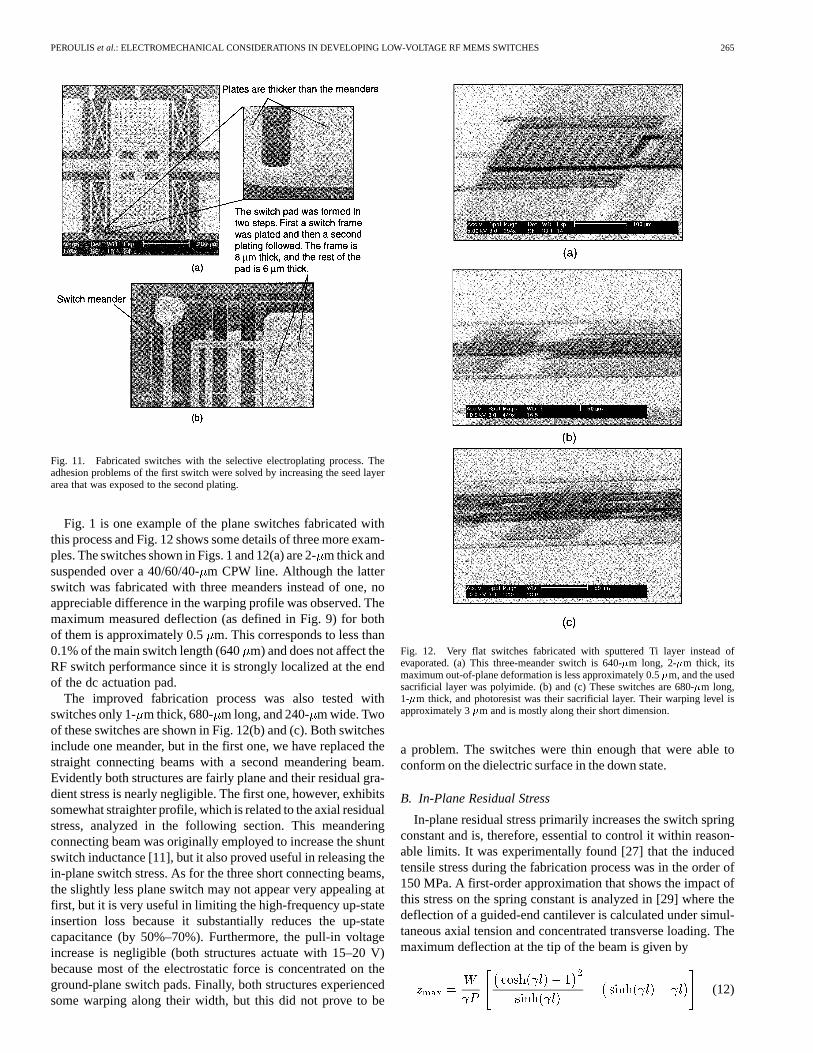
Fig. 11. Fabricated switches with the selective electroplating process. Theadhesion problems of the first switch were solved by increasing the seed layerarea that was exposed to the second plating.
Fig. 1 is one example of the plane switches fabricated withthis process and Fig. 12 shows some details of three more exam-ples. The switches shown in Figs. 1 and 12(a) are 2-m thick andsuspended over a 40/60/40-m CPW line. Although the latterswitch was fabricated with three meanders instead of one, noappreciable difference in the warping profile was observed. Themaximum measured deflection (as defined in Fig. 9) for bothof them is approximately 0.5m. This corresponds to less than0.1% of the main switch length (640m) and does not affect theRF switch performance since it is strongly localized at the endof the dc actuation pad.
The improved fabrication process was also tested withswitches only 1-m thick, 680- m long, and 240-m wide. Twoof these switches are shown in Fig. 12(b) and (c). Both switchesinclude one meander, but in the first one, we have replaced thestraight connecting beams with a second meandering beam.Evidently both structures are fairly plane and their residual gra-dient stress is nearly negligible. The first one, however, exhibitssomewhat straighter profile, which is related to the axial residualstress, analyzed in the following section. This meanderingconnecting beam was originally employed to increase the shuntswitch inductance [11], but it also proved useful in releasing thein-plane switch stress. As for the three short connecting beams,the slightly less plane switch may not appear very appealing atfirst, but it is very useful in limiting the high-frequency up-stateinsertion loss because it substantially reduces the up-statecapacitance (by 50%–70%). Furthermore, the pull-in voltageincrease is negligible (both structures actuate with 15–20 V)because most of the electrostatic force is concentrated on theground-plane switch pads. Finally, both structures experiencedsome warping along their width, but this did not prove to be
Fig. 12. Very flat switches fabricated with sputtered Ti layer instead ofevaporated. (a) This three-meander switch is 640-�m long, 2-�m thick, itsmaximum out-of-plane deformation is less approximately 0.5�m, and the usedsacrificial layer was polyimide. (b) and (c) These switches are 680-�m long,1-�m thick, and photoresist was their sacrificial layer. Their warping level isapproximately 3�m and is mostly along their short dimension.
a problem. The switches were thin enough that were able toconform on the dielectric surface in the down state.
B. In-Plane Residual Stress
In-plane residual stress primarily increases the switch springconstant and is, therefore, essential to control it within reason-able limits. It was experimentally found [27] that the inducedtensile stress during the fabrication process was in the order of150 MPa. A first-order approximation that shows the impact ofthis stress on the spring constant is analyzed in [29] where thedeflection of a guided-end cantilever is calculated under simul-taneous axial tension and concentrated transverse loading. Themaximum deflection at the tip of the beam is given by
(12)

266 IEEE TRANSACTIONS ON MICROWAVE THEORY AND TECHNIQUES, VOL. 51, NO. 1, JANUARY 2003
Fig. 13. Spring constant and pull-in voltage as a function of axial residualstress for a guided-end cantilever with simultaneous axial tension andconcentrated transverse loading.
where is the axial tensile load, is the transverse concen-trated load at the tip of the beam,is the length of the beam, and
is defined by
(13)
This leads to the following expression for the spring constant:
(14)
Fig. 13 shows the variation of the normalized spring constantand the associated actuation voltage (with respect to the springconstant and actuation voltage of zero axial stress) for an axialtensile stress of 0–300 MPa. This figure clearly demonstratesthe considerable impact of the axial stress on the switch actu-ation voltage. For instance, a tensile stress of 150 MPa wouldincrease the pull-in voltage of a switch suspended by four can-tilever beams by over three times.
The serpentine beams shown in Fig. 2 exhibit higher flexi-bility in handling the in-plane mean stress than the simple can-tilever beam. In other words, as the number of meanders is in-creased, not only is the-directed spring constant reduced, butalso the lateral ones. To show this effect, the- and -directedspring constants were calculated with a similar process to thatof Section II. The -directed spring constant can be expressedas
(15)where and are calculated by
(16)
(17)
Fig. 14. In-plane spring constants of the serpentine spring for various numberof meanders.
Similarly, the -directed spring constant is given by
(18)where
(19)
(20)
Linear FEM simulations verified the previous formulas andthe results are given in Fig. 14. From this figure, we clearly ob-serve that the spring constant of the serpentine spring is greatlyreduced as the number of meanders is increased. For instance, aspring with three meanders is 177 times more flexible along the
-dimension than a spring with one meander. As a result, such aspring can help release the axial switch stress along its long di-mension much more effectively than a spring with one meander.In other words, springs with many meanders are much more ef-fective as stress buffers than springs with one only one meander.A similar tendency exists for , which decreases by a factor of5.2 when the meanders are increased from one to five. Theseresults provide a qualitative explanation for the trends observedin Fig. 5.
IV. MEMS SWITCH DYNAMIC BEHAVIOR
Switching speed is one of the few disadvantages of MEMScomponents compared to p-i-n diodes and FET transistors.While their mass is typically very small (in the order of 10to10 kg), inertia due to mechanical movement still limits theirspeed typically in the order of a few microseconds. The fastestswitch thus far has been developed by researchers at the Mass-achusetts Institute of Technology (MIT) Lincoln Laboratories[3]. It is a very compact cantilever switch (less than 50-mlong) with a speed of approximately 1s. This very low speedis primarily due to its very small dimensions, mass, and limited

PEROULISet al.: ELECTROMECHANICAL CONSIDERATIONS IN DEVELOPING LOW-VOLTAGE RF MEMS SWITCHES 267
Fig. 15. Switching speed measurement setup (courtesy of Gabriel Rebeiz, TheUniversity of Michigan at Ann Arbor).
squeeze-film damping. It does require, however, a high pull-involtage of 50–60 V, while it is typically actuated with 70–80 V.Low-voltage switches are generally expected to be slower sincethey typically have to move a relatively large actuation area.This is particularly true if the switch is expected to operatein air or another gas environment, such as Nfor limiting thehumidify level around the structure.
The switching speed is measured by recording the change inthe power transmitted through the switch when a step voltageis applied at the bias of the device (Fig. 15) [30]. The RF inputsignal at 40 GHz is provided by an RF synthesizer, while the RFoutput signal is recorded by a high-frequency diode detector.The biasing signal is provided by a suitable combination oftwo dc power supplies and an inverter. Fig. 16 presents twotypical measurements taken with this set-up for three-me-ander switches. The measured switches were suspended amean distance of 5 m above the CPW line and the appliedbias voltage was only 20%–30% higher than their actuationvoltage. Both pull-in and release times were measured for theseswitches. Pull-in time is the time it takes the switch to touchthe dielectric underneath it. On the other hand, the time thatis required for the switch to move from the down state to itsoriginal height (or within 5% from this value) is defined as therelease time. Fig. 16 shows that the actuation and release timesare approximately 52 and 213s, respectively. However, forthe release time measurement, it takes the switch only 25s toreach its normal height, but another 190s are needed to settlewithin 5% of its original height. It is also interesting to notethat, during the first 30 s of the actuation stage, the switchdoes not move significantly. These effects will be discussed inthe remainder of this section.
To explain the experimental results, we employed a simpleone-dimensional (1-D) nonlinear model that has been adoptedby several researchers [17], [31], [32]. This model treats theswitch as a single lumped mass and applies classical Newto-nian mechanics to predict its behavior under the applied elec-trostatic force. A model that would accurately predict the dy-namic behavior of the MEMS structure should integrate a goodunderstanding of several different phenomena including elec-trostatics, mechanics, residual stress, contact forces, compress-ible squeeze film damping, and impact effects on a microscale.Many of these areas are currently under investigation and thereis not a complete model that would account for all of these ef-fects. Furthermore, our switch is a relatively large structure that
Fig. 16. Measurements of the switching time for the: (a) up–down and(b) down–up movements. Due to the diode detector, high-voltage levelcorresponds to low RF power and vice-versa.
cannot be perfectly approximated as a lumped mass. Neverthe-less, the 1-D model can be used for an at least qualitative expla-nation of the measured switch behavior and provide reasonableapproximations for the switching times.
The following equation of motion if the basic formula for the1-D model:
(21)
where is the switch mass, is the damping coefficient,is the switch spring constant in the direction of motion,isthe switch actuation area, is the initial gap, and are thedielectric layer constant and thickness, respectively,is the ap-plied dc voltage, is the electrostatic force, and is the con-tact force when the switch touches the dielectric. Several ap-proximations may be adopted for calculating the parameters inthis model. For instance, although the viscous damping can beconsidered constant for small displacements, this is not the casewhen the switch is moving completely toward the substrate. Our

268 IEEE TRANSACTIONS ON MICROWAVE THEORY AND TECHNIQUES, VOL. 51, NO. 1, JANUARY 2003
model for the switching speed calculations is based on the dis-cussion presented in [31] and [33] where these effects are takeninto account. These equations can be summarized as follows:
(22)
where (23)
(24)
(25)
Equation (24) calculates the switch quality factor and takes intoaccount the damping dependence on the switch height. If thisis ignored, the second term of the right-hand side should bereplaced by one. Furthermore, the third term reduces the gasflow resistance underneath the switch because of the slip ef-fect, where particles can have fewer interactions before escaping[34]. The variable of this term is the called the mean free pathand is approximately 0.1m at standard temperature pressure(STP). The damping coefficient, which is related toby (23),has been derived in [35] for a square plate with areaas
(26)
where is the air viscosity (at STP Pa s). Forthe switch dimensions and for a gap of m Pas and (for N/m). However, the holesincluded in the switch allow the air underneath to escape moreeasily, thus reducing the damping coefficient and increasing the
of the structure. Therefore, this value can be considered as alow bound for the switch quality factor. In fact, our experimentalresults suggest a quality factor of about two. The final equationof the model (25) was used to provide a stable solution to thesimulation when the switch contacts the dielectric layer.
Fig. 17(a) shows the simulated results for the pull-in and re-lease time. A spring constant of 8.6 N/m (Table II) and an actu-ation voltage of 25% higher than the pull-in voltage have beenused for these simulations. These simulations provide a valuableinsight in the measured dynamic behavior of the switch. Thepull-in time, for instance, is approximately 50s, from whichapproximately 30 s are needed for the switch to move from 5 to3.5 m. The RF capacitance, however, does not change appre-ciably between this distance and this explains the relatively longperiod that is required to note any difference between the mea-sured output power level (see Fig. 16). On the other hand, duringthe release stage, the switch reaches its original height within35 s, but 140 additional microseconds are required for stabi-lization within 5% of its original height. We have also plottedin the same figure the simulated release time assuming a con-stant quality factor . Evidently, taking into account thequality-factor variation versus height is of vital importance formeaningful simulations.
Fig. 17. (a) Simulated switch pull-in and release times. (b) Comparison ofsimulated release times for different values of the quality factor. (c) Comparisonof simulated pull-in times for different values of the quality factor.
The problem of the long stabilization time can be easily cor-rected by decreasing the quality factor by approximately one.Fig. 17(b) shows the simulated release time for quality factorsof 2, 1.5, and 1. This figure clearly demonstrates that the re-lease time can be decreased by more than three times if a lowerquality factor is achieved. This can be done by optimizing thehole orientation on the main switch structure and by reducingtheir number per unit area. This change will not appreciably in-crease the pull-in time, as shown in Fig. 17(c). For example, for
, the pull-in time will be increased by only 10%, yet therelease time will be reduced by 300%. Consequently, an opti-mization of the switch holes can lead to a design with switchingtimes in the order of 50–60s.

PEROULISet al.: ELECTROMECHANICAL CONSIDERATIONS IN DEVELOPING LOW-VOLTAGE RF MEMS SWITCHES 269
V. CONCLUSIONS
Low-voltage RF MEMS switches have been studied in thispaper. The design, fabrication, and testing of these structures hasbeen thoroughly discussed and switch designs with as low as6-V actuation voltages have been measured. Moreover, residualstress issues associated with this family of switches have beenaddressed and it has been experimentally demonstrated thatsputtered seed layer films result in devices with superior per-formance when compared with evaporated films. Furthermore,the dynamic operation of low-voltage switches has been experi-mentally and theoretically characterized and adequate switchingspeeds in the order of 50s have been achieved.
ACKNOWLEDGMENT
The authors are grateful to G. L. Tan, The University ofMichigan at Ann Arbor, and G. M. Rebeiz, The Universityof Michigan at Ann Arbor, for designing and developing themeasurement setup shown in Fig. 15.
REFERENCES
[1] R. E. Mihailovich, M. Kim, J. B. Hacker, E. A. Sovero, J. Studer, J.A. Higgins, and J. F. DeNatale, “MEM relay for reconfigurable RF cir-cuits,” IEEE Microwave Wireless Comp. Lett., vol. 11, pp. 53–55, Feb.2001.
[2] D. Hyman, A. Schmitz, B. Warneke, T. Y. Hsu, J. Lam, J. Brown, J.Schaffner, A. Walston, R. Y. Loo, M. Mehregany, and J. Lee, “Sur-face-micromachined RF MEMS switches on GaAs substrates,”Int. J.RF Microwave Computer-Aided Eng., vol. 9, pp. 348–361, Aug. 1999.
[3] S. Duffy, C. Bozler, S. Rabe, J. Knecht, L. Travis, P. Wyatt, C. Keast,and M. Gouker, “MEMS microswitches for reconfigurable microwavecircuitry,” IEEE Microwave Wireless Comp. Lett., vol. 11, pp. 106–108,Mar. 2001.
[4] P. M. Zavracky, N. E. McGruer, R. H. Morrison, and D. Potter, “Mi-croswitches and microrelays with a view toward microwave applica-tions,” Int. J. RF Microwave Computer-Aided Eng., vol. 9, pp. 338–347,July 1999.
[5] C. L. Goldsmith, Z. Yao, S. Eshelman, and D. Denniston, “Performanceof low-loss RF MEMS capacitive switches,”IEEE Microwave GuidedWave Lett., vol. 8, pp. 269–271, Aug. 1998.
[6] G. L. Tan and G. M. Rebeiz, “DC-26 GHz MEMS series-shunt absorp-tive switches,” inIEEE MTT-S Int. Microwave Symp. Dig., vol. 1, May2001, pp. 325–328.
[7] D. Peroulis, K. Sarabandi, and L. P. B. Katehi, “Low contact resistanceseries MEMS switches,” inIEEE MTT-S Int. Microwave Symp. Dig.,vol. 1, June 2002, pp. 223–226.
[8] J. B. Muldavin and G. M. Rebeiz, “High-isolation CPW MEMS shuntswitches—Part 1: Modeling,”IEEE Trans. Microwave Theory Tech.,vol. 48, pp. 1045–1052, June 2000.
[9] G. M. Rebeiz and J. B. Muldavin, “RF MEMS switches and switch cir-cuits,” IEEE Microwave Mag., vol. 2, pp. 59–71, Dec. 2001.
[10] S. P. Pacheco, L. P. B. Katehi, and C. T. Nguyen, “Design of low actua-tion voltage RF MEMS switch,” inIEEE MTT-S Int. Microwave Symp.Dig., vol. 1, June 2000, pp. 165–168.
[11] D. Peroulis, S. Pacheco, K. Sarabandi, and L. P. B. Katehi, “MEMSswitches for high-isolation switching and tunable filtering,” inIEEEMTT-S Int. Microwave Symp. Dig., vol. 2, June 2000, pp. 1217–1220.
[12] N. S. Barker and G. M. Rebeiz, “Optimization of distributed MEMStransmission-line phase shifters—U -band andW -band design,”IEEETrans. Microwave Theory Tech., vol. 48, pp. 1957–1966, Nov. 2000.
[13] J. S. Hayden and G. M. Rebeiz, “Low-loss cascadable MEMS distributedX-band phase shifters,”IEEE Microwave Guided Wave Lett., vol. 10,pp. 142–144, Apr. 2000.
[14] D. Peroulis, S. Pacheco, K. Sarabandi, and L. P. B. Katehi, “Tunablelumped components with applications to reconfigurable MEMS filters,”in IEEE MTT-S Int. Microwave Symp. Dig., vol. 1, June 2001, pp.341–344.
[15] J. C. Chiao, Y. Fu, J. M. Chio, M. DeLisio, and L. Y. Lin, “MEMS re-configurable antenna,” inIEEE MTT-S Int. Microwave Symp. Dig., vol.2, June 1999, pp. 1515–1518.
[16] C. Goldsmith, J. Ehmke, A. Malczewski, B. Pillans, S. Eshelman, Z.Yao, J. Brank, and M. Eberly, “Lifetime characterization of capacitiveRF MEMS switches,” inIEEE MTT-S Int. Microwave Symp. Dig., vol.1, June 2001, pp. 227–230.
[17] E. K. Chan, E. C. Kan, and R. W. Dutton, “Non-linear dynamic modelingof micromachined microwave switches,” inIEEE MTT-S Int. MicrowaveSymp. Dig., vol. 3, June 1997, pp. 1511–1514.
[18] R. K. Gupta and S. D. Senturia, “Pull-in time dynamics as a measure ofabsolute pressure,” inIEEE 10th Int. MEMS Workshop, Jan. 1997, pp.290–294.
[19] G. K. Fedder, “Simulation of microelectromechanical systems,”Ph.D. dissertation, Dept. Elect. Eng. Comput. Sci., Univ. California atBerkeley, Berkeley, CA, 1994.
[20] S. P. Timoshenko and J. N. Goodier,Theory of Elasticity. New York:McGraw-Hill, 1970.
[21] CADRE Analytic, “CADRE light, v. 1.3,” inFinite Element StructuralAnalysis Software Samammish, WA, 1999.
[22] D. Peroulis, S. P. Pacheco, K. Sarabandi, and L. P. B. Katehi, “RF MEMSswitches with enhanced power handling capabilities,”IEEE Trans. Mi-crowave Theory Tech., submitted for publication.
[23] M. T. A. Saif and N. C. MacDonald, “Planarity of large MEMS,”J.Microelectromech. Syst., vol. 5, pp. 79–97, June 1996.
[24] J. A. Thornton and D. W. Hoffman, “Stress related effects in thin films,”Thin Solid Films, vol. 171, pp. 5–31, Apr. 1989.
[25] S. M. Hu, “Stress related problems in silicon technology,”J. Appl. Phys.,vol. 70, pp. 53–79, Sept. 1991.
[26] W. Fang and J. A. Wickert, “Determining mean and gradient residualstresses in thin films using micromachined cantilevers,”J. Micromech.Microeng., vol. 6, pp. 301–309, Sept. 1996.
[27] L. Lin, A. P. Pisano, and R. T. Howe, “A micro strain gauge withmechanical amplifier,”J. Microelectromech. Syst., vol. 9, pp. 313–321,Dec. 1997.
[28] D. Peroulis, S. Pacheco, K. Sarabandi, and L. P. B. Katehi, “Alleviatingthe adverse stress effects of residual stress in RF MEMS switches,” inProc. Eur. Microwave Conf., vol. 1, Sept. 2001, pp. 173–176.
[29] R. J. Roark and W. Young,Formulas for Stress and Strain, 6th ed. NewYork: McGraw-Hill, 1989.
[30] G. L. Tan, “High-performance RF MEMS circuits and phase shifters,”Ph.D. dissertation, Dept. Elect. Eng. Comput. Sci., Univ. Michigan atAnn Arbor, Ann Arbor, MI, 2002.
[31] J. B. Muldavin and G. M. Rebeiz, “Nonlinear electro-mechanical mod-eling of MEMS switches,” inIEEE MTT-S Int. Microwave Symp. Dig.,vol. 3, June 2001, pp. 2119–2122.
[32] F. Shi, “Dynamic analysis of micro-electro-mechanical systems,”Int. J.Numer. Methods Eng., vol. 39, pp. 4119–4136, 1996.
[33] J. B. Muldavin, “Design and analysis of series and shunt MEMSswitches,” Ph.D. dissertation, Dept. Elect. Eng. Comput. Sci., Univ.Michigan at Ann Arbor, Ann Arbor, MI, 2001.
[34] T. Veijola, H. Kuisma, J. Lahdenpera, and T. Ryhanen, “Equivalent-cir-cuit model of the squeezed gas film in a silicon accelerometer,”Sens.Actuators A, Phys., vol. 48, pp. 239–248, May 1995.
[35] J. J. Blech, “On isothermal squeeze films,”J. Lubrication Tech., vol.105, pp. 615–620, October 1983.
Dimitrios Peroulis (S’91–M’02) was born inAthens, Greece, in 1975. He received the Diplomadegree in electrical and computer engineering fromthe National Technical University of Athens, Athens,Greece, in 1993, the M.S. degree in electricalengineering from The University of Michigan atAnn Arbor, in 1999, and is currently working towardthe Ph.D. degree at The University of Michigan atAnn Arbor.
His current research is focused on MEMS and theirapplications to reconfigurable circuits and antennas
for microwave and millimeter-wave frequencies.Mr. Peroulis was the recipient of the 2002 Rackham Graduate School Pre-
Doctoral Fellowship presented by The University of Michigan at Ann Arbor andthe Third Place Award at the Student Paper Competition presented at the 2001IEEE Microwave Theory and Techniques Society (IEEE MTT-S) InternationalMicrowave Symposium, Phoenix, AZ. He was also the recipient of two Stu-dent Paper Awards (honorable mentions) at the Student Paper Competitions pre-sented at the 2002 IEEE MTT-S International Microwave Symposium, Seattle,WA, and the 2001 IEEE Antennas and Propagation Society (IEEE AP-S) In-ternational Symposium, Boston, MA, and two awards for academic excellencepresented by the Technical Chamber of Greece and the Hellenic National Sci-ence Fellowship Foundation in 1997 and 1996, respectively.

270 IEEE TRANSACTIONS ON MICROWAVE THEORY AND TECHNIQUES, VOL. 51, NO. 1, JANUARY 2003
Sergio P. Pachecowas born in Salvador, Bahia,Brazil, in 1969. He received the B.S.E.E. andM.S.E.E. degrees from Auburn University, Auburn,AL, in 1993 and 1995, respectively, and is currentlyworking toward the Ph.D. in electrical engineeringat The University of Michigan at Ann Arbor.
Since May 2001, he has been a Senior Staff En-gineer with the Emerging Technologies Group, Dig-ital DNA Laboratories, Motorola, Tempe, AZ. His re-search is focused on the application of MEMS to RFand wireless applications.
Mr. Pacheco is member of the IEEE Microwave Theory and Techniques So-ciety (IEEE MTT-S) and the IEEE Electron Device Society (IEEE ED-S). Heis also a member of the Omicron Delta Kappa, Eta Kappa Nu, and Tau BetaPi Honor Societies. He was the recipient of the Judge’s Best Paper Award pre-sented at the IEEE MTT-S International Microwave Symposium in 1998.
Kamal Sarabandi (S’87–M’90–SM’92–F’00)received the B.S. degree in electrical engineeringfrom the Sharif University of Technology, Tehran,Iran, in 1980, and the M.S.E. and Ph.D. degreesfrom The University of Michigan at Ann Arbor,in 1986 and 1989, respectively, both in electricalengineering.
From 1980 to 1984 he was a Microwave Engineerwith the Telecommunication Research Center. Heis currently the Director of the Radiation Laboratoryand a Professor in the Department of Electrical
Engineering and Computer Science, The University of Michigan at Ann Arbor.He was the Principal Investigator of many projects sponsored by the NationalAeronautics and Space Administration (NASA), Jet Propulsion Laboratory(JPL), Army Research Office (ARO), Office of Naval Research (ONR), ArmyResearch Laboratory (ARL), National Science Foundation (NSF), DefenseAdvanced Research Projects Agency (DARPA), and numerous industries. Hehas authored or coauthored numerous book chapters and over 90 papers inrefereed journals on electromagnetic scattering, random media modeling, wavepropagation, antennas, microwave measurement techniques, radar calibration,inverse scattering problems, and microwave sensors. He has also had over 170papers and invited presentations in national and international conferences andsymposia on similar subjects. His research areas of interest include electro-magnetic-wave propagation, antennas, and microwave and millimeter-waveradar remote sensing. He is listed inWho’s Who in American Men and Womenof Science, Who’s Who in America, andWho’s Who in Electromagmetics.
Dr. Sarabandi is a member of the IEEE Geoscience and Remote SensingSociety (IEEE GRSS) Administrative Committee (AdCom), chairman of theAwards Committee of the IEEE GRSS, and a member of the IEEE TechnicalActivities Board Awards Committee. He is also a member of CommissionF, International Scientific Radio Union (URSI), and the ElectromagneticAcademy. He is the associate editor of the IEEE TRANSACTIONS ONANTENNAS
AND PROPAGATION and the IEEE SENSORS JOURNAL. He was the recipientof the Henry Russel Award presented by the Regent of The University ofMichigan, the GAAC Distinguished Lecturer Award presented by the GermanFederal Ministry of Education, Science and Technology in 1999, and the1996 Teaching Excellence Award presented by the Electrical Engineering andComputer Science Department, The University of Michigan at Ann Arbor.
Linda P. B. Katehi (S’81–M’84–SM’89–F’95) re-ceived the B.S.E.E. degree from the National Tech-nical University of Athens, Athens, Greece, in 1977,and the M.S.E.E. and Ph.D. degrees from the Univer-sity of California at Los Angeles, in 1981 and 1984,respectively.
In September 1984, she joined the faculty ofthe Electrical Engineering and Computer ScienceDepartment, The University of Michigan at AnnArbor, as an Assistant Professor, and then becamean Associate Professor in 1989 and Professor in
1994. She has served in many administrative positions, including Director ofGraduate Programs, College of Engineering (1995–1996), Elected Member ofthe College Executive Committee (1996–1998), Associate Dean For GraduateEducation (1998–1999), and Associate Dean for Academic Affairs (sinceSeptember 1999). She is currently the Dean of the Schools of Engineering,Purdue University, West Lafayette, IN. She has authored or coauthored 410papers published in refereed journals and symposia proceedings and she holdsfour U.S. patents. She has also generated 20 Ph.D. students.
Dr. Katehi is a member of the IEEE Antennas and Propagation Society (IEEEAP-S), the IEEE Microwave Theory and Techniques Society (IEEE MTT-S),Sigma Xi, Hybrid Microelectronics, and International Scientific Radio Union(URSI) Commission D. She was a member of the IEEE AP-S AdministrativeCommittee (AdCom) (1992–1995). She was an associate editor for the IEEETRANSACTIONS ON MICROWAVE THEORY AND TECHNIQUES and the IEEETRANSACTIONS ON ANTENNAS AND PROPAGATION. She was the recipient ofthe 1984 IEEE AP-S W. P. King (Best Paper Award for a Young Engineer),the 1985 IEEE AP-S S. A. Schelkunoff Award (Best Paper Award), the 1987National Science Foundation Presidential Young Investigator Award, the 1987URSI Booker Award, the 1994 Humboldt Research Award, the 1994 Universityof Michigan Faculty Recognition Award, the 1996 IEEE MTT-S MicrowavePrize, the 1997 International Microelectronics and Packaging Society (IMAPS)Best Paper Award, and the 2000 IEEE Third Millennium Medal.