electrochemical monitoring of tio atomic layer...
TRANSCRIPT
Electrochemical Monitoring of TiO2 Atomic Layer Deposition byChronoamperometry and Scanning Electrochemical MicroscopyAshis K. Satpati,§,†,‡ Netzahualcoyotl Arroyo-Curras,§,‡ Li Ji,§,∥,⊥ Edward T. Yu,∥,⊥ and Allen J. Bard*,§
§Center for Electrochemistry, Department of Chemistry and Biochemistry, ∥Texas Materials Institute and the Materials Scienceand Engineering Program, The University of Texas at Austin, Austin, Texas 78712, and ⊥Microelectronics Research Center,The University of Texas at Austin, Austin TX 78758, United States
*S Supporting Information
ABSTRACT: The scanning electrochemical microscope (SECM)was used to characterize the atomic layer deposition (ALD) ofTiO2 on indium-doped tin oxide (ITO) substrates by studyingelectron transfer through pores in the thin films (1−5 nmthickness). The extent of electron transfer, and thus the porosity ofthe films, was evaluated by transient electrochemistry.These studies show that ALD deposition of TiO2 on ITO doesnot produce pinhole-free films but rather porous deposits withelectrochemical behavior similar to that of microelectrode arraysup to about 30 ALD cycles. All the experimental results areexplained in the context of a numerical model developed by finite element analysis and corroborated by complementaryconductive atomic force microscopy (cAFM) results that directly reveal localized, nanoscale current conduction paths in thinnerTiO2 layers with a transition to more spatially uniform conduction in the thickest layers. SECM images demonstrate the existenceof pinholes even on films that have been subjected to more than 100 ALD cycles (thicknesses larger than 4 nm).
KEYWORDS: atomic layer deposition (ALD), scanning electrochemical microscopy (SECM), nanoporous films,finite element modeling
■ INTRODUCTION
We carried out experiments with the scanning electrochemicalmicroscope (SECM)1 to characterize TiO2 films created by atomiclayer deposition (ALD)2 on indium-doped tin oxide (ITO)substrates. In particular, we evaluated electron transfer at TiO2-coated ITO at different stages of surface coverage and in films ofdifferent thicknesses (δ = 1−5 nm). SECM is a useful techniquefor the localized evaluation of charge transfer across thin filmsbecause it allows discrimination between currents tunnelingthrough a film and those associated with pinholes.3
ALD, or atomic layer epitaxy (ALE), was developed in the1970s.4 This technique is believed to form pinhole-free,atomically smooth conformal deposits on even and unevensubstrates, thanks to its sequential and self-limiting type ofreaction mechanism.5 In the semiconductor industry, ALD hasbeen used as a standard method to deposit the diffusion barrierin metal−oxide−semiconductor field-effect transistor (MOS-FET) structures.6 Since the semiconductor industry hasundergone miniaturization in many specific applications, therequirement of producing conformal coatings with a high aspectratio has become critically important.7 ALD is the preferredchoice over other deposition techniques for conformal coatingon miniaturized devices. Furthermore, ALD plays an importantrole in the deposition of thin oxide films with high dielectricconstants like HfO2 and SrTiO3 for electronic applications,8
as well as ZnO, TiO2, and Al2O3 for electrical, mechanical,electrochemical, and optical applications.9−18 In the context of
photoelectrocatalysis, a recent publication has employed ALDdeposition of TiO2 on Si wafers to produce a robust photoanodefor photoelectrochemical water oxidation.16 The transparentoxide coatings deposited by ALD on various semiconductormaterials may play an important role in reducing photocorrosionand electrochemical decomposition of the photocatalyst, e.g.,in water splitting experiments. Some important reviews on themechanism of ALD deposition and its use in different fields areavailable.19−26
We were interested in studying the extent of electron transferthrough oxide films deposited by ALD as a function of thenumber of applied cycles. ALD is known to be a slow process,with deposition rates of 100−300 nm h−1 (only a fraction of amonolayer per pulse).27 Even though characterization of ALDdeposits has traditionally been performed by spectroscopicmethods, electrochemistry is a more suitable tool for themonitoring of charge transfer at such deposits. To the best ofour knowledge, such electrochemical studies of electron transferthrough ALD thin films have not been reported. Here, wediscuss the ALD deposition of TiO2 on ITO substrates bymultiple deposition cycles to produce different thicknesses andsurface coverage. Electron transfer with the TiO2 films wasinvestigated by chronoamperometry and voltammetry, and the
Received: May 20, 2013Revised: September 27, 2013Published: October 9, 2013
Article
pubs.acs.org/cm
© 2013 American Chemical Society 4165 dx.doi.org/10.1021/cm401635v | Chem. Mater. 2013, 25, 4165−4172
results treated by a model developed by finite element analysis.SECM experiments were also carried out to study chargetransport at localized surface regions, and to detect the presenceof pinholes in the films. These results were corroborated by
conductive atomic force microscopy (cAFM) imaging andspectroscopy that provide direct evidence of localized variationsin conduction at submicrometer length scales and a transitionfrom highly localized to more spatially uniform conduction withincreasing TiO2 layer thickness.
■ EXPERIMENTAL SECTIONInstrumentation. A Savannah ALD system from Cambridge
Nanotech (Cambridge, MA) was used for the deposition of TiO2
films. The instrument was calibrated to deposit 0.04 nm thick TiO2
films per cycle. ITO plates were obtained from Delta TechnologiesLtd. (Loveland, CO). Scanning electron microscopy (SEM) measure-ments were carried out with a Hitachi S-5500 (Dallas, TX) toqualitatively characterize the deposits. All electrochemical measure-ments were carried out with a CHI920C SECM workstation from CHInstruments (Austin, TX). A three-electrode cell configuration wasused during all electrochemical measurements. In chronoamperometricmeasurements the working electrode (ALD sample or array sample)was clamped over a hole in the bottom of the Teflon sample cell withthe exposed radius defined by the rubber O-ring (r = 0.35 cm). Thecounter electrode was a platinum wire. Potentials in this work arereported vs Ag/AgCl reference electrode.
SECM measurements were carried out in the same cell. The 10 μmdiameter platinum wire was purchased from Alfa Aesar (Wardhill,MA) to fabricate SECM tips by the methods described elsewhere.1
All SECM tips had RG = 2.0 ± 0.1. Dr. Sun Peng from East TennesseeState University kindly donated the nanoelectrode used for thedetection of pinholes in this work (Pt, 86 nm diameter, RG = 1.1 ± 0.1).Ferrocenemethanol (FcMeOH) and potassium nitrate (KNO3) werepurchased from Thermo Fischer Scientific (New Jersey) and usedas received. Solutions were prepared using a Milli-Q water system(18 MΩ). cAFM measurements were performed using a BrukerDimension Icon AFM system (Bruker Co., Germany) with diamondcoated, antimony doped silicon probe tips (DDESP-FM-10, Bruker Co.,Germany) in the contact mode.
Table 1. Conversions between Film Thickness (δ) andNumber of ALD Pulses Applieda
δ (nm) no. of pulses
1.00 251.52 382.00 503.00 754.00 1005.00 125
aConversion factor = 0.04 nm/pulse.
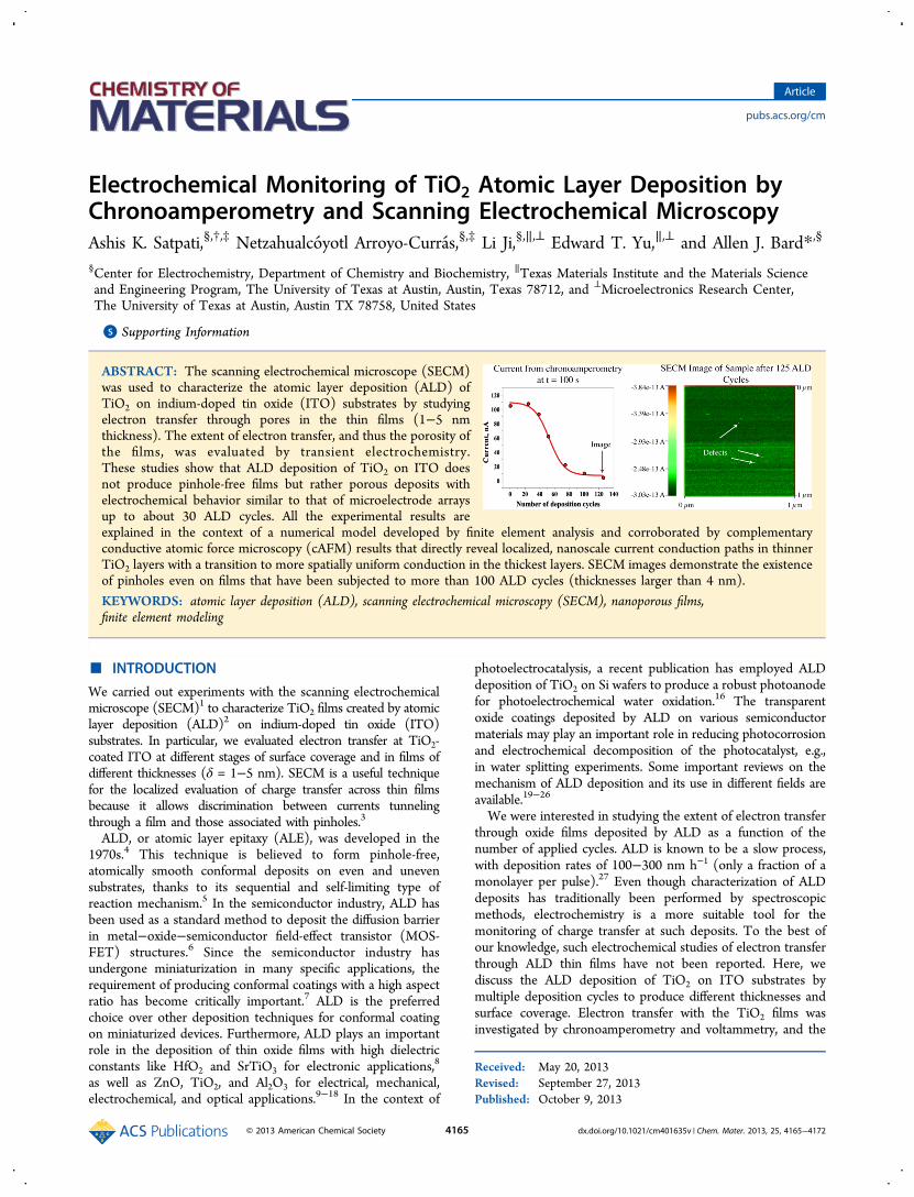
Figure 1. Chronoamperograms of 1 mM FcMeOH in 0.1 M KNO3solution at TiO2-covered ITO, logarithmic scale. Eapp = 0.5 V (E0′ =0.24 V vs Ag/AgCl). The vertical dashed line represents the time,t = 100 s, at which current was sampled to make Figure 4.
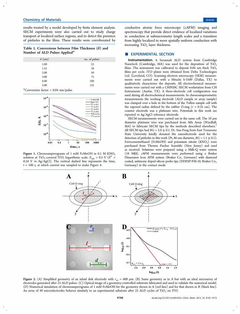
Figure 2. (A) Simplified geometry of an inlaid disk electrode with rarr = 600 μm. (B) Same geometry as in A but with an ideal microarray ofelectrodes generated after 25 ALD pulses. (C) Optical image of a geometry-controlled substrate fabricated and used to validate the numerical model.(D) Numerical simulation of chronoamperograms of 1 mM FcMeOH for the geometry shown in A (red line) and for that shown in B (black line).An array of 49 microelectrodes behaves similarly to an experimental substrate after 25 ALD cycles of TiO2 on ITO.
Chemistry of Materials Article
dx.doi.org/10.1021/cm401635v | Chem. Mater. 2013, 25, 4165−41724166
Preparation of Substrates for ALD. As received ITO plates werefirst sonicated in water (10 min) and then in ethanol (30 min) andfinally dried in an oven at 120 °C for 10 min. The cleaned ITOplates were placed inside the ALD chamber. Tetrakis(dimethylamido)titanium (TDMAT) was used as the precursor. The precursor cylinderwas kept at 75 °C for evaporation, and the deposition chamber wasmaintained at 150 °C. Detailed deposition parameters are tabulatedin Scheme S1 of the Supporting Information. An ALD depositionscheme for a similar system was previously reported.28 On precursorpulsing, TDMAT molecules were adsorbed over the ITO substrate byreleasing two molecules of dimethylaniline. On water pulsing, thetwo remaining dimethylamido groups were released leaving twounbound OH groups in the Ti center, which were available for theadsorption of TDMAT molecules arriving on repetitive precursorpulsing. The net chemical reaction scheme that produced the TiO2deposition was
+ ⇌ +[(CH ) N] Ti 2H O TiO 4(CH ) NH3 2 4 2 2 3 2
Desorbed TDMAT molecules decompose through various reactionsdescribed previously; these reaction products are nonabsorbable andflowed out of the reaction chamber by the carrier gas.29,30 The numberof deposition cycles, or pulses, was carefully controlled to producefilms with different thicknesses and surface coverage (step 14 inSupporting Information Scheme S1). The produced deposits werequalitatively examined by SEM and X-ray photoelectron spectroscopy(XPS). In selecting a substrate, we initially evaluated the quality ofTiO2 films deposited by ALD on four different substrates: Ag, Pt,fluorine-doped tin oxide coated glass (FTO), and ITO coated glass. Pt(30 nm thickness) and Ag (65 nm thickness) smooth surfaces wereprepared prior to ALD treatment by sputtering and chemical vapordeposition on Si substrates, respectively. Preliminary XPS/SEM resultsshowed that the best films were produced on ITO substrates (seeFigures S1−S7 in the Supporting Information); hence, we limited thestudies here to only TiO2 on ITO.Preparation of Samples for Testing the Theoretical Model.
The results from chronoamperometry presented in this work areexplained within the context of a model created by both theoreticaland experimental analysis. The theoretical model was developed usingcommercial software (COMSOL Multiphysics version 4.2) based onfinite element methods (FEM). The experiments were carried out ongeometry-controlled samples that mimicked the geometry employed inthe simulations. Such samples were produced by soft lithography31
with methods explained elsewhere.32 Briefly, a layer of positivephotoresist (1 mL, ∼10 μm thick, AZ P4620, AZ Electronic Materials,Somerville, NJ) was spin-coated onto a Au coated glass slide (EMFCorp., Ithaca, NY) and then exposed to UV light through positivephotomasks containing the electrode microarray designs. The photo-masks were created with Corel Draw Graphics Suit 12 and printed atCAD/Art Services, Inc. (Bandon, OR). The electrode microstructureswere transferred to the Au slides by developing the photoresist in AZ421 K solution (AZ Electronic Materials, Somerville, NJ) for 2 min.
Optical images of these samples are provided in SupportingInformation Figure S8. The substrates had an overall radius definedby the O-ring at the cell bottom that defined the area; the arrays with9, 25, 49, and 81 pores were always centered. Each individual porewithin an array was a recessed gold microelectrode surrounded by10 μm thick insulating photoresist.
■ RESULTS AND DISCUSSIONThe problem of electron transfer through thin films at thesolid−electrolyte interface has been studied extensively for thecase of self-assembled monolayers (SAM) of alkane thiols andoxide films.33 When no pinholes or defects are present (an idealsituation), electrons can tunnel through a film at a rate thatdecays exponentially with distance:33,34
= = β−k x k x( ) ( 0)e x0 0
where x is the distance over which tunneling occurs and β is akinetic factor that depends weakly on potential. However, ifpinholes or imperfections are present in the film, the extentof electron transfer also becomes a function of the size anddistribution of pores after the assembly/deposition process.This is precisely the case observed for TiO2 films generated byALD on ITO at coverages below 100 deposition cycles (δ ≤ 4 nm,see Table 1). Within that thickness range, electrochemicalmeasurements carried out on TiO2-covered substrates showedno tunneling behavior but rather an electrochemical responsethat could easily be correlated to the architecture of a film that isporous in nature.
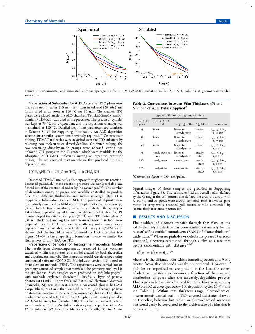
Figure 3. Experimental and simulated chronoamperograms for 1 mM FcMeOH oxidation in 0.1 M KNO3 solution at geometry-controlledsubstrates.
Table 2. Conversions between Film Thickness (δ) andNumber of ALD Pulses Applieda
type of diffusion during time transient
no. of ALDcycles
0.01 s ≤ t ≤1 sl 1 s ≤ t ≤ 100 s t ≥ 100 s parameters
25 linear linear tosteady-state
linear dc−c ≤ 15rp,rp = μm
38 linear linear tosteady-state
linear dc−c ≤ 15rp,rp = μm
50 linear linear tosteady-state
linear dc−c ≤ 15rp,rp =μm
75 steady-state tolinear
linear tosteady-state
steady-state
dc−c ≤ 5rp,rp< μm
100 steady-state steady-state steady-state
dc−c ≤ 30rp,rp< nm
125 steady-state steady-state steady-state
dc−c ≥ 30rp,rp< nm
aConversion factor = 0.04 nm/pulse.
Chemistry of Materials Article
dx.doi.org/10.1021/cm401635v | Chem. Mater. 2013, 25, 4165−41724167
Chronoamperometric Analysis. Potentiostatic measure-ments were carried out with the oxidation of 1 mM FcMeOHin 0.1 M KNO3 solution at an applied potential, Eapp = 0.5 V(E0′ = 0.24 V vs Ag/AgCl), for 1000 s. The chronoampero-grams obtained are shown in Figure 1. In the figure, thelog10 i(t) recorded at a bare ITO electrode of area = 0.38 cm2
(TiO2-free surface, black line) showed Cottrell behavior(eq 1) with a slope m = −0.59 ± 0.05 (compared to theoreticalmCottrell = −0.5, red line).
π= −i t
nFAD Ctlog ( ) log
12
log10 10
1/2
1/2 10 (1)
As the deposition of TiO2 increased with the number ofALD cycles applied, the initial magnitude of log10 i(t) decreasedproportionally to the extent of surface coverage. Also, differenttransitions in current behavior were observed in each of thesubstrates produced. For example, the chronoamperogram cor-responding to 25 ALD cycles (blue line) presented a log10 i(t)that first followed Cottrell behavior, then transitioned intoa region of smaller slope (a quasi steady-state region), and thentransitioned back into a second Cottrell decay region. Similartransitions were recorded at substrates produced after 38and 50 ALD cycles. For deposits obtained after 75 ALD cyclesor more, steady-state behavior was observed at t ≥ 100 s.This electrochemical behavior is typically observed in micro-electrode arrays, where mass transfer of electroactive speciesat one ultramicroelectrode region is time-dependent andaffected by the presence of other neighboring ultramicro-electrodes.35−41
The problem of ALD fractional coverage can be treated byFEM in a simplified geometry like the one shown in Figure 2.The reaction considered in this work is:
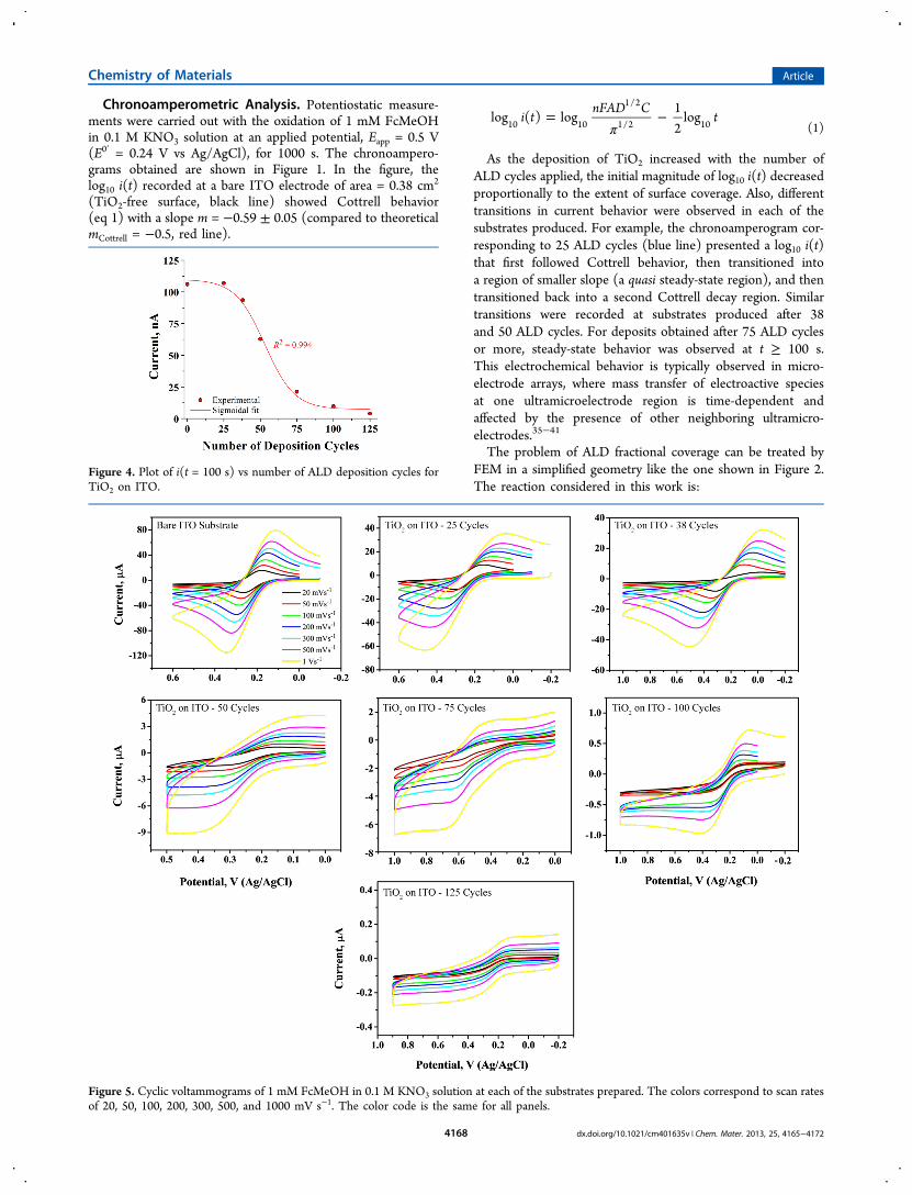
Figure 4. Plot of i(t = 100 s) vs number of ALD deposition cycles forTiO2 on ITO.
Figure 5. Cyclic voltammograms of 1 mM FcMeOH in 0.1 M KNO3 solution at each of the substrates prepared. The colors correspond to scan ratesof 20, 50, 100, 200, 300, 500, and 1000 mV s−1. The color code is the same for all panels.
Chemistry of Materials Article
dx.doi.org/10.1021/cm401635v | Chem. Mater. 2013, 25, 4165−41724168
+ ⇌+ −eFcMeOH FcMeOHk
k
b
f
where kf and kb are rate constants defined according to theButtler−Volmer formalism as
= α− −k k exp f E Ef
0 [ ( )]0
= α− −k k exp f E Eb
0 [(1 ) ( )]0
The heterogeneous rate constant is k0 = 2 cm s−1,42 α is thetransfer coefficient (α = 0.5 in this work), and f = F/RT,where F is Faraday’s constant, R the gas constant, and T theexperimental temperature. The diffusion profile of electroactivespecies is calculated by solving Fick’s second law in Cartesiancoordinates for a three-dimensional geometry:
∂∂
= ∂∂
+ ∂∂
+ ∂∂
⎛⎝⎜
⎞⎠⎟
Ct
DC
xC
yC
z
2
2
2
2
2
2
where the diffusion coefficient is D = 7.8 × 10⁻⁶ cm2 s−1.42 Foran inlaid macroelectrode, like the one depicted in Figure 2A,the current response recorded under mass transfer controlfollows Cottrell behavior (eq 1, red line in Figure 2D).However, representing the ALD partial surface coverage of TiO2on the ITO substrates as a regular array of pores (Figure 2B),the current response with time is a function of the three mainparameters illustrated in Figure 2C: the radius of the poresproduced, rp; the center-to-center distance separation betweensuch pores, dc−‑c; and the net length of the microarray, larr. Forexample, a microarray like the one depicted in Figure 2B with49 pores, rp = 37.5 μm, dc−c = 5rp, and larr = 600 μm, produces asimulated response similar to the chronoamperogram obtainedafter 25 ALD pulses of TiO2 on ITO, as shown in Figure 2D(black line). At times t ≤ rp
2/D or ∼10 s for the example here,semi-infinite linear diffusion controls mass transfer at eachindividual UME (pinhole) present on the substrate. At longertimes, e.g., t > 10 s, the currents at each UME transitions tosteady-state and the magnitude of log10 i(t) tends toward levelingoff. However, at t > dc−c
2/D or ∼100 s, the diffusion layers of allpinholes overlap to give a second transition to linear diffusion,this one characteristic of a single electrode with area larr
2. Themodel was validated by performing chronoamperometricmeasurements on substrates having surface architectures similarto the ones considered in the numerical simulations (seeExperimental Section and Supporting Information Figure S8).The comparison between experimental currents and thoseobtained from the FEM model are shown in Figure 3.Additional simulations were carried out with other parameters,
varying rp, dc‑c, and the number of pinholes to understandthe behavior of the ALD transients in Figure 1. These aresummarized in Table 2. To represent these ALD chronoampero-metric results, it is convenient to plot the current at a given timeas a function of the number of ALD cycles. A typical plot for
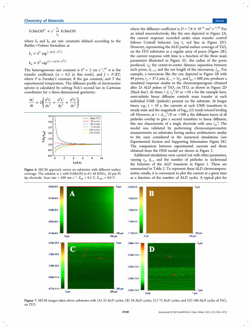
Figure 6. SECM approach curves on substrates with different surfacecoverage. The solution is 1 mM FcMeOH in 0.1 M KNO3. 10 μm Pttip electrode. Scan rate = 500 nm s−1. Etip = 0.5 V, Esubs = 0.0 V.
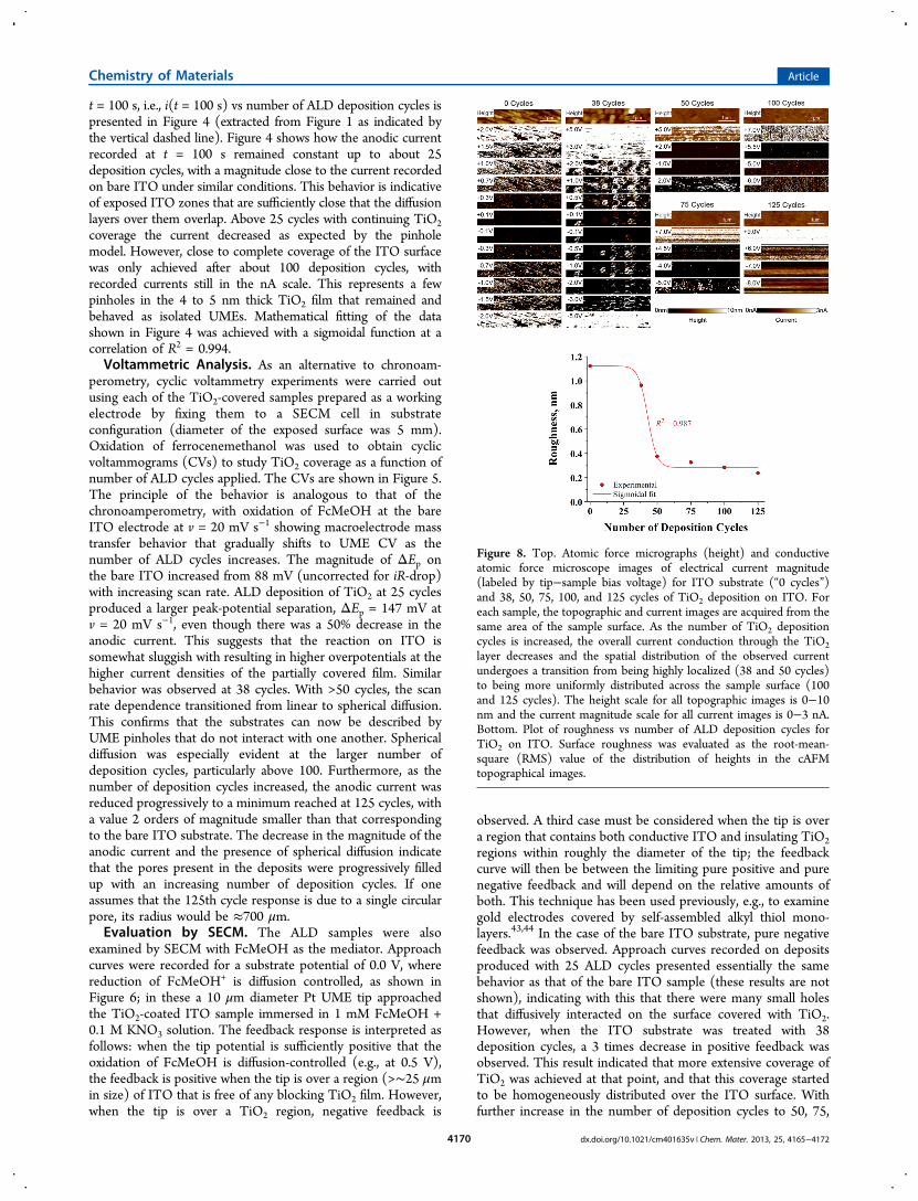
Figure 7. SECM images taken above substrates with (A) 25 ALD cycles; (B) 50 ALD cycles; (C) 75 ALD cycles; and (D) 100 ALD cycles of TiO2on ITO.
Chemistry of Materials Article
dx.doi.org/10.1021/cm401635v | Chem. Mater. 2013, 25, 4165−41724169
t = 100 s, i.e., i(t = 100 s) vs number of ALD deposition cycles ispresented in Figure 4 (extracted from Figure 1 as indicated bythe vertical dashed line). Figure 4 shows how the anodic currentrecorded at t = 100 s remained constant up to about 25deposition cycles, with a magnitude close to the current recordedon bare ITO under similar conditions. This behavior is indicativeof exposed ITO zones that are sufficiently close that the diffusionlayers over them overlap. Above 25 cycles with continuing TiO2coverage the current decreased as expected by the pinholemodel. However, close to complete coverage of the ITO surfacewas only achieved after about 100 deposition cycles, withrecorded currents still in the nA scale. This represents a fewpinholes in the 4 to 5 nm thick TiO2 film that remained andbehaved as isolated UMEs. Mathematical fitting of the datashown in Figure 4 was achieved with a sigmoidal function at acorrelation of R2 = 0.994.Voltammetric Analysis. As an alternative to chronoam-
perometry, cyclic voltammetry experiments were carried outusing each of the TiO2-covered samples prepared as a workingelectrode by fixing them to a SECM cell in substrateconfiguration (diameter of the exposed surface was 5 mm).Oxidation of ferrocenemethanol was used to obtain cyclicvoltammograms (CVs) to study TiO2 coverage as a function ofnumber of ALD cycles applied. The CVs are shown in Figure 5.The principle of the behavior is analogous to that of thechronoamperometry, with oxidation of FcMeOH at the bareITO electrode at v = 20 mV s−1 showing macroelectrode masstransfer behavior that gradually shifts to UME CV as thenumber of ALD cycles increases. The magnitude of ΔEp onthe bare ITO increased from 88 mV (uncorrected for iR-drop)with increasing scan rate. ALD deposition of TiO2 at 25 cyclesproduced a larger peak-potential separation, ΔEp = 147 mV atv = 20 mV s−1, even though there was a 50% decrease in theanodic current. This suggests that the reaction on ITO issomewhat sluggish with resulting in higher overpotentials at thehigher current densities of the partially covered film. Similarbehavior was observed at 38 cycles. With >50 cycles, the scanrate dependence transitioned from linear to spherical diffusion.This confirms that the substrates can now be described byUME pinholes that do not interact with one another. Sphericaldiffusion was especially evident at the larger number ofdeposition cycles, particularly above 100. Furthermore, as thenumber of deposition cycles increased, the anodic current wasreduced progressively to a minimum reached at 125 cycles, witha value 2 orders of magnitude smaller than that correspondingto the bare ITO substrate. The decrease in the magnitude of theanodic current and the presence of spherical diffusion indicatethat the pores present in the deposits were progressively filledup with an increasing number of deposition cycles. If oneassumes that the 125th cycle response is due to a single circularpore, its radius would be ≈700 μm.Evaluation by SECM. The ALD samples were also
examined by SECM with FcMeOH as the mediator. Approachcurves were recorded for a substrate potential of 0.0 V, wherereduction of FcMeOH+ is diffusion controlled, as shown inFigure 6; in these a 10 μm diameter Pt UME tip approachedthe TiO2-coated ITO sample immersed in 1 mM FcMeOH +0.1 M KNO3 solution. The feedback response is interpreted asfollows: when the tip potential is sufficiently positive that theoxidation of FcMeOH is diffusion-controlled (e.g., at 0.5 V),the feedback is positive when the tip is over a region (>∼25 μmin size) of ITO that is free of any blocking TiO2 film. However,when the tip is over a TiO2 region, negative feedback is
observed. A third case must be considered when the tip is overa region that contains both conductive ITO and insulating TiO2regions within roughly the diameter of the tip; the feedbackcurve will then be between the limiting pure positive and purenegative feedback and will depend on the relative amounts ofboth. This technique has been used previously, e.g., to examinegold electrodes covered by self-assembled alkyl thiol mono-layers.43,44 In the case of the bare ITO substrate, pure negativefeedback was observed. Approach curves recorded on depositsproduced with 25 ALD cycles presented essentially the samebehavior as that of the bare ITO sample (these results are notshown), indicating with this that there were many small holesthat diffusively interacted on the surface covered with TiO2.However, when the ITO substrate was treated with 38deposition cycles, a 3 times decrease in positive feedback wasobserved. This result indicated that more extensive coverage ofTiO2 was achieved at that point, and that this coverage startedto be homogeneously distributed over the ITO surface. Withfurther increase in the number of deposition cycles to 50, 75,
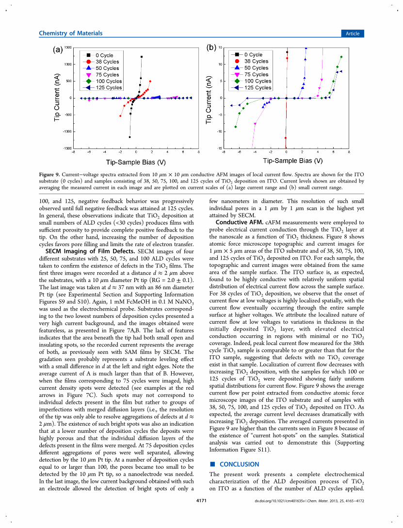
Figure 8. Top. Atomic force micrographs (height) and conductiveatomic force microscope images of electrical current magnitude(labeled by tip−sample bias voltage) for ITO substrate (“0 cycles”)and 38, 50, 75, 100, and 125 cycles of TiO2 deposition on ITO. Foreach sample, the topographic and current images are acquired from thesame area of the sample surface. As the number of TiO2 depositioncycles is increased, the overall current conduction through the TiO2layer decreases and the spatial distribution of the observed currentundergoes a transition from being highly localized (38 and 50 cycles)to being more uniformly distributed across the sample surface (100and 125 cycles). The height scale for all topographic images is 0−10nm and the current magnitude scale for all current images is 0−3 nA.Bottom. Plot of roughness vs number of ALD deposition cycles forTiO2 on ITO. Surface roughness was evaluated as the root-mean-square (RMS) value of the distribution of heights in the cAFMtopographical images.
Chemistry of Materials Article
dx.doi.org/10.1021/cm401635v | Chem. Mater. 2013, 25, 4165−41724170
100, and 125, negative feedback behavior was progressivelyobserved until full negative feedback was attained at 125 cycles.In general, these observations indicate that TiO2 deposition atsmall numbers of ALD cycles (<30 cycles) produces films withsufficient porosity to provide complete positive feedback to thetip. On the other hand, increasing the number of depositioncycles favors pore filling and limits the rate of electron transfer.SECM Imaging of Film Defects. SECM images of four
different substrates with 25, 50, 75, and 100 ALD cycles weretaken to confirm the existence of defects in the TiO2 films. Thefirst three images were recorded at a distance d ≈ 2 μm abovethe substrates, with a 10 μm diameter Pt tip (RG = 2.0 ± 0.1).The last image was taken at d ≈ 37 nm with an 86 nm diameterPt tip (see Experimental Section and Supporting InformationFigures S9 and S10). Again, 1 mM FcMeOH in 0.1 M NaNO3was used as the electrochemical probe. Substrates correspond-ing to the two lowest numbers of deposition cycles presented avery high current background, and the images obtained werefeatureless, as presented in Figure 7A,B. The lack of featuresindicates that the area beneath the tip had both small open andinsulating spots, so the recorded current represents the averageof both, as previously seen with SAM films by SECM. Thegradation seen probably represents a substrate leveling effectwith a small difference in d at the left and right edges. Note theaverage current of A is much larger than that of B. However,when the films corresponding to 75 cycles were imaged, highcurrent density spots were detected (see examples at the redarrows in Figure 7C). Such spots may not correspond toindividual defects present in the film but rather to groups ofimperfections with merged diffusion layers (i.e., the resolutionof the tip was only able to resolve aggregations of defects at d ≈2 μm). The existence of such bright spots was also an indicationthat at a lower number of deposition cycles the deposits werehighly porous and that the individual diffusion layers of thedefects present in the films were merged. At 75 deposition cyclesdifferent aggregations of pores were well separated, allowingdetection by the 10 μm Pt tip. At a number of deposition cyclesequal to or larger than 100, the pores became too small to bedetected by the 10 μm Pt tip, so a nanoelectrode was needed.In the last image, the low current background obtained with suchan electrode allowed the detection of bright spots of only a
few nanometers in diameter. This resolution of such smallindividual pores in a 1 μm by 1 μm scan is the highest yetattained by SECM.
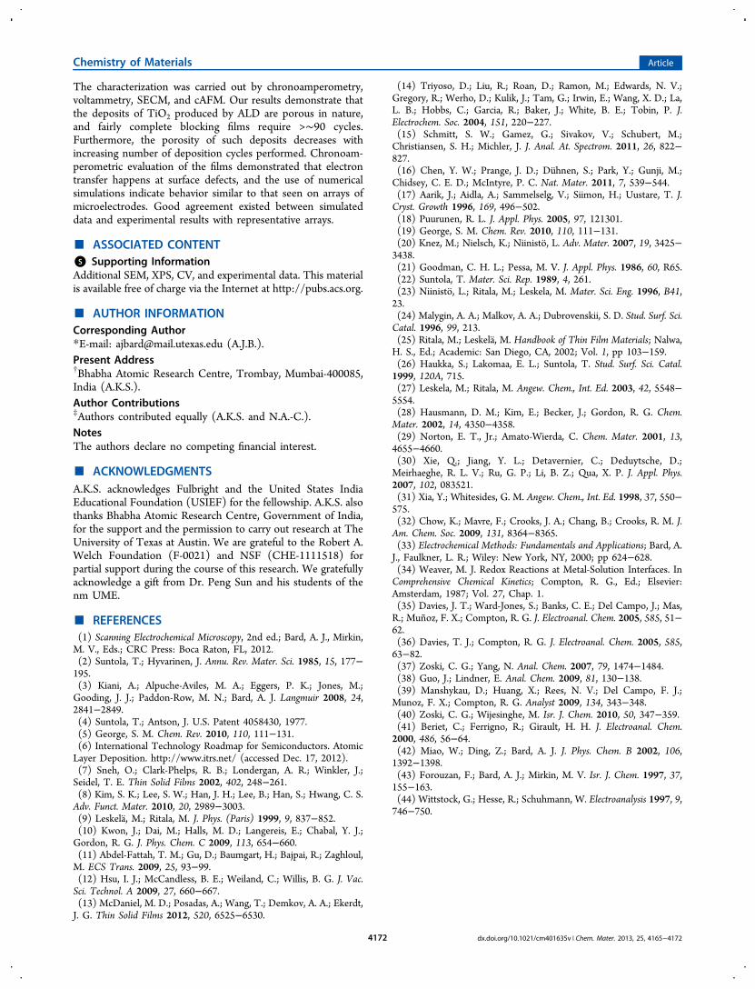
Conductive AFM. cAFM measurements were employed toprobe electrical current conduction through the TiO2 layer atthe nanoscale as a function of TiO2 thickness. Figure 8 showsatomic force microscope topographic and current images for1 μm × 5 μm areas of the ITO substrate and of 38, 50, 75, 100,and 125 cycles of TiO2 deposited on ITO. For each sample, thetopographic and current images were obtained from the samearea of the sample surface. The ITO surface is, as expected,found to be highly conductive with relatively uniform spatialdistribution of electrical current flow across the sample surface.For 38 cycles of TiO2 deposition, we observe that the onset ofcurrent flow at low voltages is highly localized spatially, with thecurrent flow eventually occurring through the entire samplesurface at higher voltages. We attribute the localized nature ofcurrent flow at low voltages to variations in thickness in theinitially deposited TiO2 layer, with elevated electricalconduction occurring in regions with minimal or no TiO2coverage. Indeed, peak local current flow measured for the 38thcycle TiO2 sample is comparable to or greater than that for theITO sample, suggesting that defects with no TiO2 coverageexist in that sample. Localization of current flow decreases withincreasing TiO2 deposition, with the samples for which 100 or125 cycles of TiO2 were deposited showing fairly uniformspatial distributions for current flow. Figure 9 shows the averagecurrent flow per point extracted from conductive atomic forcemicroscope images of the ITO substrate and of samples with38, 50, 75, 100, and 125 cycles of TiO2 deposited on ITO. Asexpected, the average current level decreases dramatically withincreasing TiO2 deposition. The averaged currents presented inFigure 9 are higher than the currents seen in Figure 8 because ofthe existence of “current hot-spots” on the samples. Statisticalanalysis was carried out to demonstrate this (SupportingInformation Figure S11).
■ CONCLUSION
The present work presents a complete electrochemicalcharacterization of the ALD deposition process of TiO2on ITO as a function of the number of ALD cycles applied.
Figure 9. Current−voltage spectra extracted from 10 μm × 10 μm conductive AFM images of local current flow. Spectra are shown for the ITOsubstrate (0 cycles) and samples consisting of 38, 50, 75, 100, and 125 cycles of TiO2 deposition on ITO. Current levels shown are obtained byaveraging the measured current in each image and are plotted on current scales of (a) large current range and (b) small current range.
Chemistry of Materials Article
dx.doi.org/10.1021/cm401635v | Chem. Mater. 2013, 25, 4165−41724171
The characterization was carried out by chronoamperometry,voltammetry, SECM, and cAFM. Our results demonstrate thatthe deposits of TiO2 produced by ALD are porous in nature,and fairly complete blocking films require >∼90 cycles.Furthermore, the porosity of such deposits decreases withincreasing number of deposition cycles performed. Chronoam-perometric evaluation of the films demonstrated that electrontransfer happens at surface defects, and the use of numericalsimulations indicate behavior similar to that seen on arrays ofmicroelectrodes. Good agreement existed between simulateddata and experimental results with representative arrays.
■ ASSOCIATED CONTENT*S Supporting InformationAdditional SEM, XPS, CV, and experimental data. This materialis available free of charge via the Internet at http://pubs.acs.org.
■ AUTHOR INFORMATIONCorresponding Author*E-mail: [email protected] (A.J.B.).Present Address†Bhabha Atomic Research Centre, Trombay, Mumbai-400085,India (A.K.S.).Author Contributions‡Authors contributed equally (A.K.S. and N.A.-C.).NotesThe authors declare no competing financial interest.
■ ACKNOWLEDGMENTSA.K.S. acknowledges Fulbright and the United States IndiaEducational Foundation (USIEF) for the fellowship. A.K.S. alsothanks Bhabha Atomic Research Centre, Government of India,for the support and the permission to carry out research at TheUniversity of Texas at Austin. We are grateful to the Robert A.Welch Foundation (F-0021) and NSF (CHE-1111518) forpartial support during the course of this research. We gratefullyacknowledge a gift from Dr. Peng Sun and his students of thenm UME.
■ REFERENCES(1) Scanning Electrochemical Microscopy, 2nd ed.; Bard, A. J., Mirkin,M. V., Eds.; CRC Press: Boca Raton, FL, 2012.(2) Suntola, T.; Hyvarinen, J. Annu. Rev. Mater. Sci. 1985, 15, 177−195.(3) Kiani, A.; Alpuche-Aviles, M. A.; Eggers, P. K.; Jones, M.;Gooding, J. J.; Paddon-Row, M. N.; Bard, A. J. Langmuir 2008, 24,2841−2849.(4) Suntola, T.; Antson, J. U.S. Patent 4058430, 1977.(5) George, S. M. Chem. Rev. 2010, 110, 111−131.(6) International Technology Roadmap for Semiconductors. AtomicLayer Deposition. http://www.itrs.net/ (accessed Dec. 17, 2012).(7) Sneh, O.; Clark-Phelps, R. B.; Londergan, A. R.; Winkler, J.;Seidel, T. E. Thin Solid Films 2002, 402, 248−261.(8) Kim, S. K.; Lee, S. W.; Han, J. H.; Lee, B.; Han, S.; Hwang, C. S.Adv. Funct. Mater. 2010, 20, 2989−3003.(9) Leskela, M.; Ritala, M. J. Phys. (Paris) 1999, 9, 837−852.(10) Kwon, J.; Dai, M.; Halls, M. D.; Langereis, E.; Chabal, Y. J.;Gordon, R. G. J. Phys. Chem. C 2009, 113, 654−660.(11) Abdel-Fattah, T. M.; Gu, D.; Baumgart, H.; Bajpai, R.; Zaghloul,M. ECS Trans. 2009, 25, 93−99.(12) Hsu, I. J.; McCandless, B. E.; Weiland, C.; Willis, B. G. J. Vac.Sci. Technol. A 2009, 27, 660−667.(13) McDaniel, M. D.; Posadas, A.; Wang, T.; Demkov, A. A.; Ekerdt,J. G. Thin Solid Films 2012, 520, 6525−6530.
(14) Triyoso, D.; Liu, R.; Roan, D.; Ramon, M.; Edwards, N. V.;Gregory, R.; Werho, D.; Kulik, J.; Tam, G.; Irwin, E.; Wang, X. D.; La,L. B.; Hobbs, C.; Garcia, R.; Baker, J.; White, B. E.; Tobin, P. J.Electrochem. Soc. 2004, 151, 220−227.(15) Schmitt, S. W.; Gamez, G.; Sivakov, V.; Schubert, M.;Christiansen, S. H.; Michler, J. J. Anal. At. Spectrom. 2011, 26, 822−827.(16) Chen, Y. W.; Prange, J. D.; Duhnen, S.; Park, Y.; Gunji, M.;Chidsey, C. E. D.; McIntyre, P. C. Nat. Mater. 2011, 7, 539−544.(17) Aarik, J.; Aidla, A.; Sammelselg, V.; Siimon, H.; Uustare, T. J.Cryst. Growth 1996, 169, 496−502.(18) Puurunen, R. L. J. Appl. Phys. 2005, 97, 121301.(19) George, S. M. Chem. Rev. 2010, 110, 111−131.(20) Knez, M.; Nielsch, K.; Niinisto, L. Adv. Mater. 2007, 19, 3425−3438.(21) Goodman, C. H. L.; Pessa, M. V. J. Appl. Phys. 1986, 60, R65.(22) Suntola, T. Mater. Sci. Rep. 1989, 4, 261.(23) Niinisto, L.; Ritala, M.; Leskela, M. Mater. Sci. Eng. 1996, B41,23.(24) Malygin, A. A.; Malkov, A. A.; Dubrovenskii, S. D. Stud. Surf. Sci.Catal. 1996, 99, 213.(25) Ritala, M.; Leskela, M. Handbook of Thin Film Materials; Nalwa,H. S., Ed.; Academic: San Diego, CA, 2002; Vol. 1, pp 103−159.(26) Haukka, S.; Lakomaa, E. L.; Suntola, T. Stud. Surf. Sci. Catal.1999, 120A, 715.(27) Leskela, M.; Ritala, M. Angew. Chem., Int. Ed. 2003, 42, 5548−5554.(28) Hausmann, D. M.; Kim, E.; Becker, J.; Gordon, R. G. Chem.Mater. 2002, 14, 4350−4358.(29) Norton, E. T., Jr.; Amato-Wierda, C. Chem. Mater. 2001, 13,4655−4660.(30) Xie, Q.; Jiang, Y. L.; Detavernier, C.; Deduytsche, D.;Meirhaeghe, R. L. V.; Ru, G. P.; Li, B. Z.; Qua, X. P. J. Appl. Phys.2007, 102, 083521.(31) Xia, Y.; Whitesides, G. M. Angew. Chem., Int. Ed. 1998, 37, 550−575.(32) Chow, K.; Mavre, F.; Crooks, J. A.; Chang, B.; Crooks, R. M. J.Am. Chem. Soc. 2009, 131, 8364−8365.(33) Electrochemical Methods: Fundamentals and Applications; Bard, A.J., Faulkner, L. R.; Wiley: New York, NY, 2000; pp 624−628.(34) Weaver, M. J. Redox Reactions at Metal-Solution Interfaces. InComprehensive Chemical Kinetics; Compton, R. G., Ed.; Elsevier:Amsterdam, 1987; Vol. 27, Chap. 1.(35) Davies, J. T.; Ward-Jones, S.; Banks, C. E.; Del Campo, J.; Mas,R.; Munoz, F. X.; Compton, R. G. J. Electroanal. Chem. 2005, 585, 51−62.(36) Davies, T. J.; Compton, R. G. J. Electroanal. Chem. 2005, 585,63−82.(37) Zoski, C. G.; Yang, N. Anal. Chem. 2007, 79, 1474−1484.(38) Guo, J.; Lindner, E. Anal. Chem. 2009, 81, 130−138.(39) Manshykau, D.; Huang, X.; Rees, N. V.; Del Campo, F. J.;Munoz, F. X.; Compton, R. G. Analyst 2009, 134, 343−348.(40) Zoski, C. G.; Wijesinghe, M. Isr. J. Chem. 2010, 50, 347−359.(41) Beriet, C.; Ferrigno, R.; Girault, H. H. J. Electroanal. Chem.2000, 486, 56−64.(42) Miao, W.; Ding, Z.; Bard, A. J. J. Phys. Chem. B 2002, 106,1392−1398.(43) Forouzan, F.; Bard, A. J.; Mirkin, M. V. Isr. J. Chem. 1997, 37,155−163.(44) Wittstock, G.; Hesse, R.; Schuhmann, W. Electroanalysis 1997, 9,746−750.
Chemistry of Materials Article
dx.doi.org/10.1021/cm401635v | Chem. Mater. 2013, 25, 4165−41724172