electricity from photovoltaic solar cells final rpt...electricity from photovoltaic solar cells ......
TRANSCRIPT

JPL Publication 86-31
Electricity from Photovoltaic Solar Cells
oo
®~
o
11 Years of Progress
Project M",rl",n~'rl the Jet

Photovoltaic Module Progress
I
l
/4I
1986
MODULE liFE
10~
1975
Typical module lifetimes were less than 1 year butare now estimated to be greater than 10 years.(Ten-year warranties are now available.)
cJ2>--
(/)U cc:z <£.w wU >-LLLLW
5
10-----MODULEEFFICIENCY
MODULE PRICE
//
75
1----r5L ---'1975 1986
Flat or non-concentrating module prices have droppedas module efficiencies have increased. Prices are in1985 dollars for large quantities of commercial products
wUccCL
0<:«wCL
lI«~<J>
Technology advancement in crystalline silicon solar cellsand modules (non-concentrating).
Union Carbide Corporation (UCC) tunded the nowoperational silicon retinement production plant with1200 IviTlyear capacity. DOEIFSA-sponsored effortswere prominent in the UCC process researchand development.
The autornateoi rna chine interconnects so/ar cellsano; places thern ror rnodule assenlbly. The secondgeneration machine made by Kuliel,e and Solla wascost shared by Westinghouse Corporation and OOEIFSA
A Block I module (fabricated in 1975). held in front of fourBlock V modules, represents the progress of an 11-year effort.The modules, designed and manufactured by industry to FSAspecifications and evaluated by FSA, rapidly evolved dunngthe series of module purchases by DOEIFSA
5101-289
Flat-PlateSolar Array Project
DOEfJPL-1012-125
Distribution Category UC-63b
Electricity from Photovoltaic Solar Cells
Flat-Plate Solar Array ProjectFinal Report
Volume IV: High-Efficiency Solar Cells
M. LeipoldL.ChengT. DaudA. MokashiD. Burger
11 Years of Progress
October 1986
Prepared for
U.S. Department of Energy
Through an Agreement with
National Aeronautics and Space Administration
by
Jet Propulsion Laboratory
California Institute of TechnologyPasadena, California
JPL Publication 86-31
Project Managedby the
Jet Propulsion Laboratory
for theU.S. Department of Energy's
National Photovoltaics Program

This FSA Final Report (JPL Publication 86-31,5101-289, DOE/JPL 1012-125, October 1986) is composed of eightvolumes, consisting of an Executive Summary and seven technology reports:
Volume I: Executive Summary.
Volume II: Silicon Material.
Volume III: Silicon Sheet: Wafers and Ribbons
Volume IV: High-Efficiency Solar Cells.
Volume V: Process Development.
Volume VI: Engineering Sciences and Reliability.
Volume VII: Module Encapsulation.
Volume VIII: Project Analysis and Integration.
Two supplemental reports included in the final report package are:
FSA Project: 10 Years of Progress, JPL Document 400-279, 5101-279, October 1985.
Summary of FSA Project Documentation: Abstracts of Published Documents, 1975 to 1986, JPL Publication 82-79(Revision 1), 5101-221, DOEIJPL-1 012-76, September 1986.
Upon request, this FSA Final Report (JPL Publication 86-31) and the two supplemental reports (JPL Document400-279 and JPL Publication 82-79) are individually available in print from:
National Technical Information ServiceU.S. Department of Commerce5285 Port Royal RoadSpringfield, VA 22161
Ii
The Flat-Plate Solar Array (FSA) Project, funded by the U.S. Government and managed by the Jet PropulsionLaboratory, was formed in 1975 to develop the module/array technology needed to attain widespread terrestrial useof photovoltaics by 1985. To accomplish this, the FSA Project established and managed an Industry, University, andFederal Government Team to perform the needed research and development (R&D).
The High-Efficiency Solar Cells Task was assigned the objective of understanding and developing high-efficiencysolar cell devices that would meet the cost and performance goals of the FSA Project. The need for research dealingwith high efficiency devices was considered important because of the role efficiency plays in reducing the price perwatt of generated energy.
This document is a summary of the R&D efforts conducted during the period 1982 to 1986 to provide understanding and control of energy conversion losses associated with crystalline-silicon solar cells. New levels of conversionefficiency (greater than 20 %) were demonstrated. Major contributions were made both to the understanding andreduction of bulk and surface losses in solar cells. For example, oxides, nitrides, and polysilicon were all shown to bepotentially useful surface passivants. Improvements in measurement techniques were made and Auger coefficientsand spectral absorption data were obtained for unique types of silicon sheet. New modeling software was developedinclUding a program to optimize a device design based on input characteristics of a cell. Although considerableprogress was made in this Task, several elements of research were incomplete at the conclusion of the Project.
iii

Throughout U.S. history, the Nation's main source of energy has changed from wood to coal to petroleum. It isinevitable that changes will continue as fossil fuels are depleted. Within a lifetime, it is expected that most U.S. energywill come from a variety of sources, including renewable energy sources, instead of from a single type of fuel. Morethan 30 % of the energy consumed in the United States is used for the generation of electricity. The consumption ofelectricity is increasing at a faster rate than the use of other energy forms and this trend is expected to continue.
Photovoltaics, a promising way to generate electricity, is expected to provide significant amounts of power in years tocome. It uses solar cells to generate electricity directly from sunlight, cleanly and reliably, without moving parts.Photovoltaic (PV) power·systems are simple, flexible, modular, and adaptable to many different applications in analmost infinite number of sizes and in diverse environments. Although photovoltaics is a proven technology that iscost-effective for hundreds of small applications, it is not yet cost-effective for large-scale utility use in the UnitedStates. For widespread economical use, the cost of generating power with photovoltaics must continue to bedecreased reducing the initial PV system cost, by increasing efficiency (reduction of land requirements), and byincreasing the operational lifetime of the PV systems.
In the early 1970s, the pressures of the increasing demand for electrical power, combined with the uncertainty offuel sources and ever-increasing prices for petroleum, led the U.S. Government to initiate a terrestrial PV research anddevelopment (R&D) project. The objective was to reduce the cost of manufacturing solar cells and modules. Thiseffort, assigned to the Jet Propulsion Laboratory, evolved from more than a decade-and-a-half of spacecraft PV powersystem experience and from recommendations of a conference on Solar Photovoltaic Energy held in 1973 at Cherry
New Jersey.
This Project, originally called the Low~ost Solar Array Project, but later known as the Flat-Plate Solar Array (FSA)Project, was based upon crystalline-silicon technology as developed for the space program. During the 1960s and1970s, it had been demonstrated that photovoltaics was a dependable electrical power source for spacecraft. In thistime interval, solar-cell quality and performance improved while the costs decreased. However, in 1975 the costs werestill much too high for widespread use on Earth. It was necessary to reduce the manufacturing costs of solar cells by afactor of approximately 100 if they were to be a practical, widely used terrestrial power source.
The FSA Project was initiated to meet specific cost, efficiency, production capacity, and lifetime goals by R&D in allphases of flat-plate module (non-concentrating) technology, from solar-cell silicon material purification through verification of module reliability and performance.
The FSA Project was phased out at the end of September 1986.
Iv

n
A Solar Cell Advisory Committee, under the direction of T. Daud and M. Leipold and chaired by M. Wolf, wasestablished to assist in directing the technology development related to solar cells. It met 22 times on an approximately triannual basis. Its members included R. Davis (deceased), P. lies, F. Lindholm, J. Loferski, E. Ralph, B. Ross(deceased), G. Schwuttke, and C. Wrigley.
Jet Propulsion Laboratory (JPL) staff members were involved in laboratory research, technology critiques,process and problem analyses, and the technical management of contracts. A. Kachare was Manager of this programto which the following JPL engineers contributed: P. Alexander, D. Burger, L. Cheng, R. Cockrum, G. Crotty, T. Daud,K. Dumas, B. Gallagher, P. Grunthaner, S. Hyland, M. Leipold, A. Mokashi, P. Seshan, R. Stirn, G. Turner, andO. von Roos (deceased).
Greatly appreciated is the assistance of E. Christensen, J. Murry, and I. Bengelsdorf in editing this document, andof S. Montanez, V. Guzman, and M. Koop in its typing.
This document reports on work done under NASA Task RE-152, Amendment 419, DOE/NASA IAADE-A101-85CE89008.
v
the tA,'hr,rMYH/L.crvv'c<' lifetime, and a sel
reduction in the manufacture of solar cells and
nrrllAI:t was nitiated inlarge
IJ'VUU\AO PV modules1975 dollars). The
to meet the stated goals research andrp,r,l'1lrll'1 from silicon-material refinement through
tA,'hrln!rV'i1i efforts with pro-"'A,rl'Y1,ttori cost-goal allocations to be made
~1'(';nl"\rY1'1' analvs,es, ,",A,·frwl'Y11".rI peri(xJil::;alliy, nArrnlt!"'rI assessment of each technicalm "0 til nn Prr\iOf,t'c progress toward the National goal. the most promising
c:n,(in(~nr R&D in organizations and universities, and led tothat to achieve advancement in PV
centrai-station it is estimated that the ofneed to be 71kWh (1985 basis for a DOE Five-Year Photo-
Ihli'nlli'lnr both increased cell and module lifetime. Area-related costs for PVthat module efficiencies must be raised to between 13 and 17%, and module
research solar ceils have been fabricated with more15% efficient module also has been fabricated. It is calculated that a
modules that the latest crystalline siliconis believed that 7/kWh (1985 is
Esltablisrled basic themodules and arrays terrestrial use. Module durabi also has been evaluated. These resulted in:
PV module a factor 5 from (1985 to (1985 aOllar~;).
efficiencies 5 6% 1975 to more than 15% in 1985.1f](1' ,<.;,,'\/ to establish 1O-year warranties on modules. There were no warranties in 975.
a new, low-cost h silicon feedstock-material refinement process.Esltablisrlinq knc)wl,edcle and for PV and evaluation.
@ PV module enlca~)sulatioj
@ manufactu cost economic analyse:3.Transferred to the sector nteractive activities i researc and fielddemonstrations. These included 256 module and evaluation26 10 research forums, at hundreds of technical and ad-
"',",OI'"t,1' technical nrn,niC,rnQ
'I< a viable commercial nited States.


critical to its performance. Modeling also provided a means to evaluate research beforeattempted and provided direction to the other research elements within the Task. Several specific programswere developed, including one to optimize predicted solar cell These programs and programs obtainedfrom other sources were installed in JPL computers. Specific analyses of existing solar cells were made andagreement of model calculations with measured performance successfully demonstrated the validity of the modeling.Calculations for theoretical solar cell designs were made and used to direct the Task research.
Specialized measurement techniques were developed to permit measurement of specific loss-parameters as wellas the electrical output of a solar cell. The measurement of carrier lifetime and surface recombination velocity in thethin, highly doped emitter region was especially important. Determination of characteristics such as Auger coefficientsand absorption coefficients for the unconventional types of silicon sheet also were made.
The Task made numerous important contributions to the understanding and improvement of silicon PV devices.The overall effectiveness of these studies best can be demonstrated by the increase in measured crystalline-siliconsolar cell performance from 17 % to > 22 % during the period of the Task's existence. Although all of the improvedcells were not produced under direct support of this Task, the contribution of the Task is clear. These cellsdemonstrate that the fabrication of very high performance, crystalline silicon cells is feasible, the cells are ofsmall size, and used expensive processes and high-cost float-zone silicon for their Clearly, these develop-ments must be extended to include silicon sheet, processes and sizes that are consistent with large-scale low-costproduction processes.
Therefore, at the conclusion of the Project, some Task activities must be described as Principally, thedetailed nature of the bulk and surface loss mechanism requires better understanding and application of the understanding to the unconventional types of silicon sheet. All of the highest performance solar celis use FZ silicon wafers,a high-cost source of silicon sheet. Replacement of this source by a lower cost material that will still thesehighest efficiency cells is needed. Better as-grown sheet quality and/or better means of reducing losses areAdditional research is necessary to complete these studies. Technical developments will continue after the conclusionof the FSA Project with part of the support, at least, coming from DOE.
viii

I. INTRODUCTION
A. BACKGROUND.
B. TASK ACTIVITIES: 1982 to 1986. 2
BULK LOSSES. 7
A. INTRODUCTION 7
B. LIMITS TO BULK LOSS IN HIGH-EFFICIENCY SILICON SOLAR CELLS: C.T. SAH ASSOCIATES. 8
C. OXYGEN AND CARBON IN SILICON: STATE UNIVERSITY OF NEW YORK AT ALBANY 8
D. STRUCTURAL AND CHEMICAL DEFECTS: CORNELL UNIVERSITY 10
E. HEAVY DOPING AND OTHER BULK EFFECTS IN HIGH-EFFICIENCY SILICON SOLAR CELLS:UNIVERSITY OF FLORIDA 11
F. HEAVY DOPING EFFECTS IN EMITTER: STANFORD UNIVERSITY. 11
G. SILICON SHEET BY MOLECULAR BEAM EPITAXY: UNIVERSITY OF CALIFORNIA, LOS ANGELES 12
H. HYDROGEN PASSIVATION. PENNSYLVANIASTATEUNIVERSITY . 13
STRUCTURAL DEFECTS: JET PROPULSION LABORATORY. 14
J. ABSORPTION COEFFICIENT MEASUREMENT: JET PROPULSION LABORATORY. 17
K. PRESENTSTATUS. 7
L. KEY ACCOMPLISHMENTS. . 7
M. FUTURE NEEDS. 17
SURFACE LOSSES . 19
A. INTRODUCTION. 19
B. SILICON SURFACE PASSIVATION BY SILICON NITRIDE: JOINT CENTER FORGRADUATE STUDY THE UNIVERSITY OF WASHINGTON 19
C. SURFACE PASSIVATION BY HEAVILY DOPED POLYCRYSTALLINE SILICON:UNIVERSITY OF FLORIDA 21
BARRIERS: STANFORD UNIVERSITY. . 22
E. MICROCRYSTALLINE SILICON HETEROJUNCTION: APPLIED SOLAR ENERGY CORP. ANDBOSTON COLLEGE 23
F. X-RAY PHOTOEMISSION SPECTROSCOPY: JET PROPULSION LABORATORY. 24
G. CONDUCTING POLYMERS: JET PROPULSION LABORATORY. 25
PRI=S;F:NT STATUS 26
26
J. EEDS
Ix
27

46
47
NEEDS 47
49
49
8.
x

VII. REFERENCES
APPENDIXES
APPENDIX A: ACQUISITION OF REFERENCES
APPENDIX B: GLOSSARY
Figures
1.
2.
:rv"t;::JllinA Silicon Solar Cell
Ant-V()ltriIOA Curve of a Hir,h_f=ffil~i"'i"'('\j Solar Cell
3
3. Key Factors that Influence Cell i=ffi('i""n('\! 3
4. High Resolution TEM Picture of the Tilt of Silicon.
5. Calculated AMO ffir·i",rl(,\/ of a Cascade Cell Versus interface Recombination \/pl(")('rfl/ 3
6. Rutherford Backscattering Data in the rhOlnln",iinn and Random Mode from Silicon ~"n-nnl"c
Subjected to Ion Beams
7. EBIC rhlotC!grc~P~ls of an Area of a Dentritic Web Ribbon Solar Cell 5
8. EBIC Photographs Taken from Three Different Areas of"as-grown" Silicon Dendritic-Web Ribbon at Room 6
9. Schematic of PECVD System 20
10. Valence Band of 13 ASi02 Over Si [1 23
11. Conduction Band of 13 A Si02 Over SI [1 00] 24
12. XPS Si 2p Spectra Obtained as a Function of Silicon Nitride Thickness 25
13. Conductivities
14. Electrochemical '-:\lI,th"CIC of ~""\!nJ\lrr,,,'.D\
15. Model Calculations for the Effect of Electrical fj. ("'''/ii'\! of the Twin Plane on in 0.2 Q-cm Web Cells
16. Twin Planes in Web c::h,.... \Alinn of Dislocations on ""Hi",,,,n,,\! 32
17. LBIC Scans of Beveled 33
18. Floating Emitter Solar Cell Transistor
9. Baseline Process Sequence
20. Calculated Solar Cell Parameters for Dot Junctions with 1
33
35
36
21 . Electronic Circuit Used in the SCCD ~A"th,,!ri
Current Decay on a ScaleSchematic Illustration of the
22. Contour Plot of the rms Data ASLBIC ~Aolh",ri\ 43
23. Schematic Cross-Section of a Passivated Thin Silicon Soiar Ceil
24. '-:oncrtl\/lt\/ of i=ffi('ic,n('·\! of Solar-Cell Thickness for Various ~A,r!",rrhi Carrier Lifetime Values
44
44
25. of Practical Barriers on Silicon Ceil Performance
xi
45

26. Impact of Shadowing and Surface Recombination Velocities on Silicon Solar Cell Performance.
27. High-Low Junction Voltage, (measured) Versus Cell Applied Voltage
Tables
1. Theoretical Limits and Typical Losses in High-Efficiency Solar Cells
2. Contractor List for High-Efficiency Device Task.
3. Performance of Silicon Solar Cells as a Function of Various Loss Mechanisms
4. Performance of Molecular-Beam Epitaxy Silicon Solar Cells
5. Comparison of Optical Constants Determined from Ellipsometry and Ordinary Reflectance ..
6. Summary of Measured Parameters at 28°C Without Antireflective Coating.
7. Flat Band Potentials of p-Si as a Function of Conducting Polymers
8. Comparison of the Light I-V Data of the Silicon Solar CellsPassivated by Si02 and TiOxlAI203
9. Dot Junction Solar-Cell Results and Corresponding Efficiency.
xii
46
46
2
4
9
13
21
22
26
35
36

u
Present solar cell conversion efficiencies are:
In selecting loss mechanisms for within thisTask, careful attention was to the fundamentalnature of the and its For
several losses of both cells andmodules were not considered because are wellunderstood and their solution is a matter ofengineering and Theseinclude anti reflective andmodule considerations such as cell pac;klrig
celi shape, module size, etc, Other tasks in theFSA developed these aspects of the tech-nology, Results of these efforts can be found inVolume V: Volume VI:no,~rir,r1 Sciences and , and VolumeModule Enl:::ar)suilatlon
inrroc,cir)r! as a result of: efforts to betterunderstand how solar cells function, better understand
of their internal loss mechanisms, better celland processing,
small advances the years have added to theknl)wleclqe of solar cell and to Increased
Early progress in cell andtOf'hnlr11 was largely This has
SUiOSE:;qlJeriIlY been better theoreticalu of the nnnr,ni~;c of cell oper-ation, These activities have led to a agreementrp(l::lrrlirln the factors that limit cell and tothose that can be to increase the ofcr\lst(±llirle-:sili(~on soiar cells, Table 1 shows lossescells that occur as a result of a of effects andthat have an Infiuence on all of the performanceparameters, The difference between a measuredparameter and its theoretical maximum provides anexcellent to the to be addressed,
Thus, the objective of the Hlclh-IEtflcIE;ncvCell Task 1 was to research to irio,nti'fllresolve generic limitations to ,nC'rOClCIr'n offiC';or\r\lof crystalline-silicon solar cells,
975, terrestrial Oh,otCivoltRiC6 % efficiency were available from rninll~'nt;,nn::ll
talline silicon, solar cell tor'hnnlr'n\/1970s, as various research and de',jel,:mrnelltefforts in the Flat-Plate Solar Arrayceeded, it was seen that the original goal of10% module efficiency would be met as a result of theongoing FSA efforts, It was this wouldoccur as solar cell efficiencies and as mod-uIe factors increased active solar cellarea per unit of module area), cell effi-ciency should increase as ceil and fabricationtechnology matured, Module factors of 0,90were to be achievable, up from the 0,60 to0.70 common in 1975,
By the early 1980s, numerous economic analysesof large PV power systems indicated that module efficiency must be about 15 % for photovoltaics to beeconomically competitive, These analyses were basedon the premise that central station PV installationswould be the first of nhc)tOl/ol-taics in the United States, The achievement of 15 %efficiency moduies requires the repeatablefabrication of large-area solar cells with 20 %or greater efficiency, This would demonstrate that high-efficiency solar cell are understood, Present-day cells in this range are too smallto be considered for solar modules, Thisknowledge then must be converted into a technology oflow-cost cell that would uniformproduction cells of 17 to 18 % efficiency needed tomodules with efficiencies 5 %
The goal of the Device Task wasto establish solar cell technology required for repeatable fabrication of solarcells with greater than 20 % OH"C'ic,nr'lI
(1) Production cells made from Czochralski (Cz)wafers for use space 8 %),
Production cells made from Cz wafers for low-cost terrestrial use to 14 %),
A, BACKGROUND (3) Production cells, made from silicon rlh,'v')r,c(greater than 13 %),
The need for from spacecraftsolar cell arrays motivated research forefficiency cells, The research broadened with the reai-ization that had the to becomea practicai terrestrial power source, theefficiency of silicon solar cells has been
Research cells made from float-zonesilicon (22 %), (The theoretical limitof efficiency for crystalline-silicon celis isabout 30 %, and the maximumachievable limit of efficiency is about 25 %),
1Within the FSA this was known as the Device Research Task,

Table Th.on!>cti.f'ol Limits Losses in I-Effic:/RllC\I Solar Cells
Values of Loss (%)Loss
Cel!Demonstration
Cel!Production
Cell
I;nllt_rt"n"r~,t"r current Ith,yvohr'", limit 44 ml' lomL
Optical reflection
Oontact coverage
Recombination
Dead
l\chieved current
a 3,0 50
0 30 30
0 5.0 20
a 0 0
44,0 393 357
In open circuit Ithe",r,,,t;r,,,1 limit:::: 0.837
Recomb!nationsurface, rrv,b,'t",\ a 15,0 350
I-{""~rlr,,,,n n::Jl>rnIMi,'n, current ieaka~le o
Ach!eved voltage (VodC 0.837 071 054
factor
V'Ji'nun above
Recombination in deiJ!etion zone
Series/contact resistance
Achieved fill factorC
Resultant "Hin;"n",.
ceii
levels,
a 130 150
0 1,0 20
0 1.0 20
096 0.82 078
35,0 22.8 17.1
CAmount r"n,OJrllnr after aPIJlicaticm of losses to theoretical limits
1982 986
the silicon material,
ne,norol tC'f'hninol aoprOEtch was establisr!edthan 20 %, The
achieveexact cell
modificationslab':Jratory cells

,'r';C:!'Q/I:"nA Silicon Soiar
SOLAR
~~"+--ARCOATING
t=:~====~:2======8ACKSURFACE FiELDr.::. BACK METAL CONTACT
3. Factors that Influence Cell Eff.iciE?ncv
2. JrrEmt- V()/tcl0e Curve of a Hiclh-.Eff,iciEmc:v
Cl "-br',,, recombination ofcarriers within a solar cell is the of cm/s.An effort to reduce the to less than 1 cm/saddressed of recombinationlosses at surfaces and interfaces. better understandand control surface and interface nhcn.'-VY10rlQ
asultrathin silicon dioxideReliable measurement Tnr·hr,in,
characterize n"C:C:I\IOllntc:of surface loss inves1 igclticlns
('nlnrl"rtllnn materials ",n,nr'Olcli7~lrl
nnl\I"',"'r with a silicon surface the resultantand electrical characteristics.
understand and control buik-Iossimnrljlu'mpntc: in silicon sheet struc
are lea(jlriqA
spc,cific metaillc on cell per-r",r,nrbrl In Volume . Silicon MateriaL
com~Jilc;ated and varied nature of siiicon sheet is afunction of its conditions and its nr(){'~lC:C:lnn
nrr,n,,,rticc and those ofthat
Solar Cell
3

i-able 2. C'onlraci' List for l-iicl/7-,EffJ'ciElnc:v [j1ev/ce Task
BuH<: Losses
953289:
956·989: Studies crf and C~arbo!-l~Related
Defects in Silleo!'"': Solar C·911s
956525: Surlace and AlliedStudies in Silicon So1ar Cells
956233: Silicon Sheet with Molecular-8eam~n,D"\1 TOi~ Soia( Cells
957~159: Carrier -r"rmC'r..nc:- ii'"'l
Siiicon
956046: Electclcal Struc"lu(al j cUid Cirjeii:icaiCI18r3c"ter!zatior'i o'{ Siiicoi'"] Slieet iVlaterfal
------------~----------- _.._------_._-------- --"'- ..
C~_T_ SCSJ--I J\ssociates
State CiT
i\~e\f\! \(0(1{
Gainesville, :=:orida
Stan-~:ord
Stanford; 'California
956960: JrrtedaciEd Studies
9566-14: CellSur-face Passivatiorl
956525- Surfa.ce and /-\!Iied Studies
BostOi~! 1 [V~8.ss8.chusetts
i\/J{)(';"d,nn and ~j1easure('ne(HS
957170: Silicorl iVlethoc:s andSiiicon Soiar Ceil i\iumerical MethodS
956741 . Computerili1nr1olinn of Silicon Solar Ceil
i={esea:-chResearchNorth Caro!'ina
956290- andSoiar Cei Is of Near 20 % i=ffi";,,,nr'\!
956467: Ti nI8-i=iesolved;:;pecirm;cc;plc iV1easu(ern8n-~s
0'( Siiicon
Table 2.
Contractor /\ddr8SS
Ceil Processes
955080: S: icon Soiar '~eli F'rocess:=abricatici'\ a('~ci
"L\SECCalifo(('iia
956786 r-..r.i i\j'c;i i
ASECof Ca!i"fornie.
Oi' 1011 Cells
StLidie;s \jv'itliii'"'j 'tl'lls Te~sk
eiectron andinc:uded
l x-ray ci~!a(8cterization

Radiative recombination: nh(,tn,1"
Thermal recombination: nhem"n"
be understood.
(1) Intrinsic mechanisms (intorr":",,., t,,,,n,,,iti,"w'lC'
The two of recombination processes inintrinsic and extrinsic with their energy
ov,~h"nr\o are ):
recombination: third electron hole.
them.
hole.recombination:
Therma! recombination
Radiative recombination: nh"tn"C'
Extrinsic mechanisms InQnrLYv"
The fundamental differences between intrin"ir·
extrinsic recombination mechanisms can be describedas follows:
(1) For the intrinsic processes, the carrierrecombination occurs via band-to-band transitions. Because the energy gap between thebands is these processes areiess than the extrinsic mechanisms.
For the extrinsic processes, the orstate is a bound state iocalized
an or defectin the gap and the other is an un!ocalizedband state. Because the
7
Oxygen is a ubiquitous impurity in silicon material,whether the silicon is single crystalline, polycrystalline,or amorphous. In Cz-grown single crystalline and castpolycrystalline silicon, the oxygen concentration istypically about 1018 atoms/cm3, which is approximatelythe solubility limit of oxygen in silicon near the melting
Even though in FZ silicon, the concentration isabout 1015 to 1016 atoms/cm3, that amount is stillsufficient to cause complications, especially followingvarious high temperature fabrication processes. It isknown that the existence of active recombination centersinvolving oxygen concentrations of the order of 1013 to1 4/cm 3 can drastically reduce the minority carrierlifetime in silicon. The existence of oxygen in concentrations several orders of magnitude higher is likely tohave noticeable effects on the recombination in siliconvia some indirect means.
In as-grown silicon, oxygen is uniformly distributedUU'''i' I\JUt the material in the form of isolated oxygen
atoms as bonded interstitials in a puckered configuration between two silicon atoms. Using the stress-induceddichroism the movement of oxygen in silicon can be detected at temperatures as low as about300 ae. evidence has shown that thebehavior of oxygen is very complicated. It is knownthat oxygen-related donors are formed during thermal
nn'''''',nn at 450 to 650 cC. can interact withvacancies and self-interstitials to form complexes thatare often mobile at these temperatures. Details of thishot'''\lII''\C no\Ne'v'er are not clear at present.
C. OXYGEN AND CARBON IN SILICON: STATEUNIVERSITY OF NEW YORK AT ALBANY
Researchers at the State University of New Yorkat investigated the presence ofoxygen and carbon in silicon and their influence onsolar cell performance. This was generic research tounderstand the behavior of oxygen and carbon insiiicon and their relationships to bulk losses in siliconsolar cells. The importance of the presence of oxygenand carbon in silicon photovoltaics is not obvious, anda brief discussion of its relevance is given below.
which substitutional sites inas-grown silicon, is electrically neutral, but can bedetected infrared thecarbon concentration silicon is about 1 to1 6 atoms/cm 3, except in EFG ribbon which issaturated with carbon. It is known that carbon interactswith intrinsic defects such as vacancies and
oxygen, and acceptorimpurities at elevated Frommental it is expected that carbon caninfluence the carrier lifetime in silicon, but itsdetailed influence is not clear at nrc,c:p,nt
It is obvious from the above that improvement ofthe of the effects of oxygenand carbon on silicon solar cell per-formance is needed for the development of highott,r,,'nr'\! and low-cost silicon solar cells for terrestrial
The effects of oxygen and carbon could
C.T. Sah and Associatesamong the recombination
processes, the intrinsic and radiative mecha-nism pose the ultimate limit and the extrinsic SRHmechanism is the current iimit. The lattercan be eliminated means of R&D to under-C't"nriinr< of the behavior of and structuraldefects in silicon as well as and cellfabrication. Innovative cell structure also mustbe to alleviate on drinn,pnt
These fundamental studies led to quantification ofmany of the features of the ideal cell. It wasshown that the ideal ceil has the lowest intrinsic recombination losses (interband radiative and interbandrecombination losses), and has no surface and interfacerecombination losses. Study by C.T. Sah Associates ofan ideal silicon cell with the common n+ - p- P+device structure shows that the ultimate efficiency,limited radiative recombination alone, is about 25 %at AM1 and 28 cC. The Auger recombination limitswere for low and high levels, andboth are close to the 25 % radiative limit. The resultsgive the condition at which SRH recombination loss willbecome to lower the ultimate efficiency.
a SRH recombination lifetime of 100 p.,s givesthe SRH base lifetime must be
r<rc>"t"r than about 1 ms to reach 25 %. This is at thelimit of the state of the art for very large scale
silicon Table 3 showsthe of silicon solar cells, theeffect of surface recombination and other losses.Details of the calculation are available IRp,fp(pnr'pc:
and 2).
B. liMITS TO BULK LOSS IN IGH-EFFICIENCYSILICON SOLAR CELLS: C.T. SAH ASSOCIATES
Details of these results, reported the above-mentioned contributing organizations, are presented inthe following sections.
C.T. Sah Associates has investigated the reiationship of material properties to high-efficiency solar cellperformance. The investigation included basic studiesof the material parameters that limit the performanceof high-efficiency silicon solar cells. The work alsodealt with identification of the barriers that prevent theachievement of the ultimate of silicon solarcells.
have included studies of effects usingconcentrations greater than those used in most
conventional semiconductors of Florida andStanford An examination was made of thepotential of a new silicon growth method, Molecular-Beam Epitaxy [University of LosAngeles, and the utility of hydrogen passiva-tion (Pennsylvania State University). In principle, it wasfound that it is possible to eliminate most of the bulklosses in the solar cell by the crystal growthand cell processing techn.iques.
8

of Silicon Solar Cells as Various Loss
Used Results
Fillcmls mA mV Factor %
3.1 36.0 81 0.86 25.4
Table
Recombination
36.0 786 0.90 25.4
36.0 776 0.86 24.0
36.0 746 0.85 23.0
36.0 634 0.83 9.1
36.0 666 0.74 17.8
36.0 442 0.66 0.6
diode
50
50
14
0.33
4000
4000
B
2
leaka~le current
2
2/3
2.3x10- 5
3.0x1
8.0x10- 15
8,Ox1
6.4x10- 13
6.4x1
L
Ohmic H
SRH
Ohmic
"'ff,:.rtl\/'" surface recombination VRIOClllV
==
== 24°C
Cell area ==
base 007B == ==
100
intrinsic carrierni ==
== base thickness == 50
N base carrier concentration ==
D == carrier diffusion coefficient == 20 cm2/s
m = of non-ideal II IT1,r'tirln diode
== electronic
== 0.62 x 1 == == 2.8 x 1
be indirect Interactions with otherand defects. The contract activities at
SUNYA were directed toward this and consider-able progress was made. The final reviews
defects in oxygen-related defects and their evolution from
isolated interstitial oxygen (Reference 3). SUNYA alsocarried out on effectsstresses on the formation of oxygen thermal donors Insilicon 4) and theoretical studies on thermaldonor formation kinetics (References 5 and SUNYA"""-fnr'm,,,ti theoretical and studies to
9
improve the understanding of the influence of oxygenand carbon-related defects on minority carrier lifetimein silicon.
D. STRUCTURAL AND CHEMICAL DEFECTS:CORNELL UNIVERSITY
Structural defects and impurities in silicon dictatethe electrical properties of the material. Scientists atCornell University (see TCJble 2) have investigated thephysical and chemical nature of structural defects inthin silicon sheets (such as web and EFG ribbons) aswell as polycrystalline wafers. They have made significant contributions to the improved understanding ofthe nature of structural defects and impurities in thesesilicon sheets and of their influence on electrical properties. Their work has covered a wide range of materials and characterization tools. The following areseveral illustrations of their accomplishments.
Understanding the influence of carbon on variousproperties of the ribbon is very important to the development of advanced silicon technology for PV applications because carbon is the major impurity in EFGribbons. Because the carbon content in Cz-grown silicon is too low for carbon to precipitate out, carbonbased gettering has not been considered in the past.The gettering mechanism, however, is important for anunderstanding of the behavior of EFG ribbon. The contractor developed a model for electrical activity ofcarbon-self-interstitial agglomerates (Reference Themodel used the assumptions that the self-interstitialcontent of these agglomerates determines their electrical activities and that compressive stresses (high, selfinterstitial content) and tensile stresses (low, selfinterstitial content) give rise to electrical activity of theagglomerates. The self-interstitial content of carbonrelated agglomerates may be reduced by appropriatehigh-temperature treatment, and enhanced by supersaturation of self-interstitials generated during formation of the p-n junction of solar cells. It has been suggested that oxygen present in supersaturation incarbon-rich silicon may be reduced to form Si02 precipitates by self-interstitials generated during phosphorus diffusion. It has been proposed that the Si-Si02interface of the precipitates gives rise to a continuumof donor states. These interface states are responsiblefor at least a part of the light enhancement effectsseen after phosphorus diffusion into oxygen-containingEFG silicon.
A considerable amount of work has been done oncharacterization of structural defects in a variety ofsilicon sheet materials for solar cell applications. Thetools used included chemical etching, electron-beaminduced current (EBIC), and transmission electronmicroscopy (TEM). Emphasis has been on the correlation of data obtained and identification of defects. Forexample, results have shown that the coherent twinboundaries in silicon are often electrically inactive, butunsymmetrical tilt boundaries are strongly active. EBICresults also have illustrated that exposure to hydrogen
10
plasma increases charge collection efficiency (Reference 8). The oxygen content in silicon dendritic webribbons also was studied. Results have shown thatoxygen content in the ribbon is similar to that in Czgrown silicon (Reference 9). An investigation of theinteractions of twin boundaries and dislocations insolar silicon also was made (Reference 10).
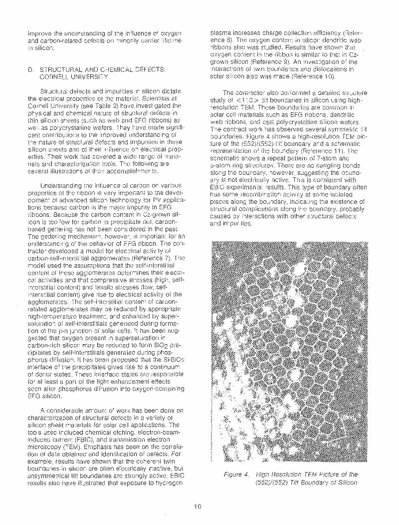
The contractor also performed a detailed structurestudy of < i 10> tilt boundaries in silicon using highresolution TEM. These boundaries are common insolar cell materials such as EFG ribbons, dendriticweb ribbons, and cast polycrystalline silicon wafers.The contract work has observed several tiltboundaries. Figure 4 shows a high-resolution TEM picture of the (552)/(552) tilt boundary and a schematicrepresentation of the boundary (Reference 1i). Theschematic shows a repeat pattern of 7-atorn and5-atom ring structures. There are no dangling bondsalong the boundary, however, suggesting the boundary is not electrically active. This is consistent withEBIC experimental results. This type of boundary oftenhas some recombination activity at some isolatedplaces along the boundary, indicating the existence ofstructural complications along the boundary, probablycaused by interactions with other structural defectsand impurities.
Figure 4. High Resolution TEM Picture of the(552)1(552) Tilt Boundary of Silicon

E. HEAVY DOPING AND OTHER BULK EFFECTS INHIGH-EFFICIENCY SILICON SOLAR CELLS:UNIVERSITY OF FLORIDA
In silicon solar cells, the base region usuallyconsists of good quality silicon with a long minoritycarrier lifetime compared to the thickness. This causesminority carriers to recombine at the back contact,which results in increased dark current and reducedopen circuit voltage. To reduce the effective surfacerecombination velocity, a high-low junction is formedat the back surface to act as a minority carrier reflector. This effect then manifests itself as effective surfacerecombination velocity (Seff) at the high-low junction.
The emitter in the solar cell generally is a very thinlayer (1000 to 3000 A thick) of heavily doped n-typematerial. Heavy doping in emitter (and base) causestwo detrimental physical phenomena that are important for solar cell operation. They are Auger recom·bination (causing lower minority carrier lifetime) andnarrowing of the bandgap (causing higher leakage currents and an electric field gradient in a direction topush the minority carriers away from the junction).
The University of Florida initially developed atransient method called Electrical Short-Circuit CurrentDelay (ESCCD) for the measurement of Tn and Seff(References 12 and 13). This method is more accuratethan the open-circuit voltage decay (OCVD) or theJunction Reverse Recovery (JRR) methods, becauseof quicker removal of injected charge in the spacecharge region.
Additional efforts were devoted to determinationof the bulk properties of heavily doped silicon. Measurement of the activation energy for arsenic-dopedsilicon at 1020 atoms/cm3 gave evidence for values ofminority-hole diffusivity, D, and mobility, /l, that are sig·nificantly lower than the majority-carrier D and /l(Reference 14). Measurement of the transit time forboron·doped silicon at 1020 atoms/cm3, usings-parameter techniques, gave similar results forminority electron /l and D (see Reference 3). Theseresults differ from those from research at Stanford University. An improved determination of bandgap nar·rowing from activation energy, however, gave resultsconsistent with Stanford results. Further work may beneeded to obtain an explanation for the two sets ofdata obtained at the two universities.
Theoretical investigations of solar cells, includingthe effects and mechanisms of the effects in heavilydoped silicon, started with an improved model forbandgap narrowing (Reference 15). It was determinedthat neither a real inhomogeneity, nor the presence ofa high surface recombination velocity reduced accuracy. Auger lifetime, Tau, was determined using photo·luminescence decay, provided one observed the tail ofthe response. This treatment led to a precise definitionof the tail. The overall conclusion is that the DzewiorSchmid values of Tau do not suffer from inadequacy oftheoretical interpretation. This lends greater credibilityto these values because they had been challenged by
11
other workers. A generalized reciprocity theorem waspresented (Reference 16) that enables calculation ofinternal quantum efficiency based on a non-illuminatedanalysis. Other applications of this analysis couldinvolve measurements of various device parameters.Thus, interfacial surface recombination velocity at apolysilicon contact could be measured by usingsteady-state or transient photons or mass-particleradiation. The mathematical foundation underpinningthe analysis of impact Auger lifetime led to an exactsolution of three~imensional transport problems forsolar cells without solving the actual boundary-valueproblem. In this theoretical work (Reference 17),recombination current, transit time, and open-circuitvoltage are determined not by solving the actual threedimensional boundary-value problems, but rather byintroducing auxiliary one~imensional models.
The earlier work on the generalized reciprocitytheorem led to the first detailed attempt to systematizethe design of silicon solar cells. Design principlesfollow from three theorems. Several optimal designsare derived from the theorems, one of which involvesa three-dimensional morphology in the emitter region.A multiple integral series solution was derived fornonuniformly and heavily doped emitter regions (Refer·ence 18). By truncation, this approach yields many different orders of approximation. It is believed that thesimplest of these approximations, called tr,equasineutral-quasiequilibrium approximation, enableshand calculations to have an accuracy comparable todetailed computer solutions provided that the emitteris thin « 3 /lm) and has a low surface recombinationvelocity « 105 cm/s).
From additional experimental studies, evidence waspresented for excess carrier storage. This phenomenonwas connected to a bandgap narrowing (80 mV or threethermal voltages for a density of 4 x 10¹⁸ atoms/cm3),not in heavily doped silicon but rather in highly excitedsilicon (Reference 19) in which approximately equalnumbers of holes and electrons exist in densities above1017 atoms/cm3. These findings have implications forsolar cells in concentrated illumination, both in thequasineutral and junction regions. A detailed interpretation was presented to explain why the apparenttransient photoconductivity lifetime can considerably
. exceed the steady-state lifetime.
F. HEAVY DOPING EFFECTS IN EMITTER:STANFORD UNIVERSITY
The Solid State Ele'ctronics Laboratory of StanfordUniversity performed an investigation of minoritycarrier transport in heavily doped p-type silicon. Theobjective was to improve the understanding ofminority carrier transport in the heavily doped emitterregion of silicon solar cells.
From first principles, the contractor demonstratedthat there are three transport and recombination parameters in heavily doped n-type silicon: (1) hole equilibrium concentration, Po, (2) lifetime, T, and (3) diffusion
L. In steady state, however, combinationsor derivations of these three fundamental parametersare relevant. The two parameters of interest are thediffusion length and the product of the hole equilibriumconcentration and the diffusion coefficient, where thediffusion coefficient is derived from the equation D =L2/T . These two parameters have been measured inheaviiy phosphorus-doped silicon fabricated by epitaxy. Good quality epitaxial layers were grown withdoping levels up to 1.6 x 10²⁰ atoms/cm3. The measurement was done on test structures with vertical andlateral bipolar transistors fabricated with the epitaxiallayers. The diffusion length in the n+ epitaxial regionwas measured from the collector characteristics ofidentical p++ - n+ - p++ lateral transistors with different base widths. Simultaneously, the hole equilibrium concentration/diffusion coefficient product wasextracted from the collector characteristics ofp++ - n+ p vertical transistors. A doping range oftwo orders of magnitude was covered. Previoussteady-state measurements of the hole transport andrecombination parameters by other authors werereviewed. The original measurements of the two relevant parameters were reconstructed from the reporteddata. Agreement within a factor of two was obtainedamong this work and other published data.
Based on Stanford's recent measurements of holelifetime in n-type silicon, values for hole mobility andhole equilibrium concentration were obtained from themeasured parameters. The hole mobility is found to betwo times larger than its p-type silicon value. The equilibrium hole concentration is about a factor of twolarger than predicted from values of bandgap narrowing measured by photoluminescence.
Using only the two measured parameters, thework also revealed that modeling of the currentini,,'r-t"'r1 into heavily doped regions is possible insteady-state. As an illustration, the emitter saturationcurrent of several bipolar transistors was calculatedand the value, without any adjustable parameters, waswithin 30 % of the experimentally measured data. Asimple and accurate analytic approximation to internai
efficiency of heavily doped emitters also wasdeveloped.
Functional doping dependence of hole lifetime,hole mobility, and bandgap narrowing were determined. These values should be useful for devicemodeling (References 19, 20, and 21). The contractoralso conducted similar research on heavily dopedp-type silicon.
G. SILICON SHEET BY MOLECULAR-BEAMEPITAXY: UNIVERSITY OF CALIFORNIA,LOS ANGELES
This effort was to apply the capabilities of the newtechnique of Molecular-Beam Epitaxy at UCLAto the growth and fabrication of high-efficiency siliconsolar cells. UCLA was to use MBE to grow and characterize silicon films and p-n junctions to determine the
12
MBE film It then was to fabricate variousprC)toltvpe hinh-At1'1r-II~nr'\i solar cell designs such as front-and back-surface cascade cells, and thenmodel and characterize these cells.
The UCLA MBE System consisted of a modifiedstainless steel Varian station capable of abase pressure of 5 x 10-11 Torr. Surface analysisincluded low energy electron diffractionelectron spectroscopy (AES), and quadrupole massspectroscopy (OMS) for in situ surface studies. Amolybdenum crucible with a 6 kW electron bombardment gun was used for pure silicon evaporation. Thebeams of gallium (p-type dopant) and antimony (n-typerl,."."",nt\ were generated resistance-heated, pyro-lytic, boron nitride effusion cells.
Normal operation consisted of cleaning the substrate by heating to 1200 °C for 1 to 2 min and checking the cleanliness by LEED pattern. Silicon films thenwere grown by moiecular beam deposition atsubstrate temperatures of 650°C. was obtainedby controlled coevaporation of either Ga or Sb. Siliconsubstrates and MBE-grown p- and n-type layers wereevaluated before and after cleaning within the chamberand after growth of each layer. Solar cells were madefrom the p-type grown layer by conventional thermaldiffusion of phosphorus and application of acontact.
was found that the cleaning procedure (heating thesubstrate to 1200 °C under < 10-9 Torr pressure) didnot degrade the minority carrier lifetime in the substrate.Solar cells made from the grown p-Iayer (-1 /lmhowever, showed very poor performance, as comparedto control cells.
Scanning Ion Microprobe Spectrosocpy (SI onthese samples showed a rise of thegrown layer rather than a after a steeperdoping rise. Also, carbon contamination was observedat the substrate-epi interface. Oxygen and carbonwere detected within the thickness of the epi-Iayer.Corrective actions such as argon bombardment priorto growth, etc., were not very successful.
Saturation current is a very sensitive test for thequality of diodes. Mesa diodes were etched on theepitaxial layer samples and a measurement of thereverse current characteristics showed that the centralregion was better than the end regions nearthe holding clamps. This was to be a result ofstresses introduced the arrangement.Minority carrier lifetime derived from the reversesaturation current measurements on p-n havebeen in the nanosecond range instead of the microsecond range normally obtained with goodsilicon.
A new substrate holder with a radiative h"",tir,(]
element was with no r-I",n-..nlnrl r"'''H 1I,'",rl
holder gave better of h",,~tirl(]
any mechanical stresses. Problems ofremained unsolved.

CASCADE CELLREAR BASE a-emFRONT BASE 0.1 Q·em
4.0
14.5
15.0
16.5
;JZ
>-' 16.0uzwUu:: 15.5LLw
7.0
17.5
Fabrication of p-nvery poorsolar cells onciencies up to 4.8 % without AR "r."tir,,,
some of the cell characteristics.
Table Performance of Molecular-Beam EpitaxySilicon Solar Cells
Hall studies on both p- andshowed that silicon matched bulk mobilityvalues at levels> 8/cm 3. TEMstudies of the films showed some areas where disloca-tion density was < 103/cm 2 . areas had disloca-tion densities of with moderatelevels of C't~,,,vin,,
cm/s
o13.5
Figure 5. Calculated AMO Efficiency of a CascadeCell Versus Interface RecombinationVelocity
this effort, nearly 30 samples of differentstructures were made. About 10 solar cells wereattempted, and the best efficiencies were 4.8 % at100 mW/cm2 illumination without AR Othersamples were used for layer characterization, diodecharacterization, and SIMS analysis.
Even though the MBE technique has the advantage of achieving sophisticated solar cell structures,nrr,hlcHY1C of quality of the layers need to be solvedbefore the technique can be applied to thefabrication of research solar cells.
mV Factor %
MBE 9 27.0 380.0 0.55 2.8
109 21.9 454.9 0.707 4.7
110 23.5 486.7 0.713 4.8
102 Shorted
103
1 2 Lost in
113 Lost in
The po.ssi,ble role of h"rirr,,,r,,., in siliconror,rr.\Alth and diffusion.
HYDROGEN PASSIVATION: PENNSYLVANIASTATE UNIVERSITY
(1) The effect of low-energyon surface properties.
At Pennsylvania Stateresearchers have established that InvIJ-AnArOV
gen can result in hy,drc)g€,n-{~alJsed
all three parts of a solar cell: emitter, soac\:;-cnai'oe, and base. This work studied:
twice theThe cell had
contact. The conceptand the model were at but a
was carried out at UCLA. It wasriiff,r>rn,,.,t bulk of the front and
""m";"",,,nll of the cascade cell wasThis was
VAIOrIT\; at the
13

(3) space-eharge region, and basepassivation.
Hydrogen passivation of bulk silicon impuritylevels.
(5) The use of hydrogen ion implants for highefficiency Cz, FZ, and OW silicon solar cells.
The significant results of these studies were:
(1) Low-energy ion beams were found to introduce structural damage at the silicon surface.This damage manifested itself as a positivesurface charge and drastically affected thecharacteristics of metal/ion-beam-damagedsilicon contacts.
Structural damage at the silicon surfaceenergetic H+ ions was found to be moreextensive than damage introduced by inertgas ions, e.g, Ar+ (Figure 6). Note that as theenergy of the incident ions is increased, moredamage is introduced at the silicon surface.Note also that H + ions introduce more latticedamage than do Ar + ions. It was found thatH+ , however, could passivate its self-inducedstructural damage, provided the sample wasallowed to thermally float during the processing. If the processing temperature wasrestricted, then the self-induced damage couldnot be passivated.
(3) Enhanced interstitial population during ionbombardment can lead to enhanced diffusivityof deep-level impurities. This, in turn, can
CHANNELING MODE
modify the concentration of these centers inthe bulk.
(4) Hydrogen, bonded to residual defects in thesilicon lattice, is stable up to temperaturesaround 600°C.
(5) Low-energy hydrogen implants can result inhydrogen-caused effects in all three parts of asolar cell: emitter, space-eharge region, andbase. In web, Cz, and FZ material, low-energyhydrogen ion implants reduced surfacerecombination velocity and also passivatedspace charge region recombination centers.
Hydrogen implants can alter the diffusionproperties of some ions implanted in silicone.g., boron (but not others, e.g., arsenic).
STRUCTURAL DEFECTS: JET PROPULSIONLABORATORY
The effect of structural defects on bulk losses isan important issue for the performance of all polycrystalline silicon solar cells. The polycrystalline materialsinclude OW ribbons, EFG ribbons, and cast siliconwafers. Line and two-dimensional structural defects,such as dislocations and grain boundaries, are themain concern because they are commonly recombination active. There has been considerable effort at JPLto improve understanding of the behavior of thesedefects and their influence on silicon solar cell performance. Following is a brief illustration of theprogress made through in-house research at JPL.
RANDOM MODE
o...JW
;:.0 KeV Ar
0.4 KeV Ar
1.0 KeV H
(b)
ENERGY ENERGY
Figure 6. Rutherford Backscattering Data in the Channeling and Random Mode fromSilicon Samples Subjected to Low-Energy Ion Beams
14

investig'3.ticlil of recombination-active structuraldefects observed in the cross section of web ribbonshas been carried out (see Reference 28). 8shows EBIC pictures of three different areas of a cross
.F. Shih, communi-7 shows two EBIC pictures of the same
area of a web solar cell taken at 298 and 110 K. Theat 298 K is almost featureless, except for a num-
ber of small black caused dustcles on the surface. The EBIC picture taken at 110 K,however, reveals interesting features: many black dotsand lines at which EBIC signals are consid'erably lowerthan those in the bulk. The two black lines that are
the ribbon axis are nrf"',h"hl"
caused low-angle grain boundaries formed theagglomeration of slip dislocations. A significant number of the black dots are preferentially alignedtwo directions about 30 deg off the axis. It isknown from previous investigations of etching thatslip dislocations in the middie of the web ribbon are likelyto be in the same pattern (see Reference 25).This and further results led to the conclu-sion that these black dots are caused slip dislocations(R~!fAren(~e 29). The measure-ments of EBIC signals at slip dislocations indicated thatrecombination activities at dislocations are not thesame, but on the of their structures.When two or more dislocations aggregate together, therecombination increases wasconcluded some disiocations have weak EBICsignals at iow temperatures and the signal disappears at160 K, whereas other dislocations disappear \:jl C!UU'dlly
over a wide range and can be active atroom The difference between the two typesis not understood.
Recombination ncr,no,rtt"" of the dislocationsin web ribbons were studied the EBIC in a scan-
Silicon dendritic web ribbon is grown a< 211 > orientation with [111] surfaces. Struc-
the ribbon consists of two thin sheets of singlecrystals twinned to each other. The twin consistsof an odd number of closely spaced, coherent twinboundaries. The existence of the twinlei to the ribbon surfaces is needed for stableof the dendrites. There also are dislocations and,occasionally, a few defects in theribbon. There are two of dislocations: (1) grown-in dislocations along the < 211 > or < 11 0> axesIrn,-,inh, in and near the twin plane), and slip dislo-cations l'ormed because of plastic deformationthe of. To understand the basicmaterial influence on the of solarcells made from web dendritic silicon, the FSA Projecthas carried out in-house research on properties ofthese structural defects.
The distribution of slip dislocations in silicondendritic ribbons was studied the technique ofchemical and The resultsshow the existence of two stresscpr,;,.",,, across the ribbon formed thedeformation stage' shear stress at the ribbonand tensile stress at the middle 25). Thisobservation is consistent with the theoretical analysisof thermal stress distribution done(References 26 and and JPL F. Shih, private
Studies have further illustrated thatof thermal stress caused
deformation the cooling can be esti-mated from the density of 28).
1 o K
G
Figure 7 EBIC Photographs of an Area of a Dendritic Web Ribbon Solar Cell
15

Figure 8. fBIC Photographs Taken from Three Different Areas of a Cross-Section of an "as-grown"Silicon Dendritic Web Ribbon at Room Temperature
section of an as-grown ribbon sample perpendicuiar tothe growth direction. These pictures illustrate severalim',",I'"II·t""t observations of recombination-active defectsin the ribbon. The distribution of these defects not onlyvaries significantly across the thickness of thebut also along the width of the ribbon. The variationsare believed to be related to the growth condition. Thedefects are concentrated in the inner of theribbon, specifically at and near twin planes, whereasthe region near the surface often has significantlyfewer defects. This Observation could be related totwo possible mechanisms occurring during growth.The first observation is the fact that the twin plane canact as a source for the creation of structural defectsand the surface can act as a sink for defects. Thesecond observation is related to theduring growth, the silicon material near the ribbonsurface often solidifies first because of the coolerenvironment around the ribbon. As a consequence ofthese two mechanisms, more structural defects areexpected to be formed in the inner part of the ribbon.The variation of defect densities along the width andthickness also can be related to some uncontrolledfluctuations of the existing growth condition.
The dark straight line parallel to the ribbonsurfaces in Figure 8 is caused by recombinationactivity at the twin plane. It is known that a perfect,coherent twin boundary is not recombination-active.This observation illustrates that the twin plane is oftenheavily decorated with recombination-active structuraldefects. There are several clearly observable segments of the twin plane, however, at which no recom-
16
bination activities are observed. This observationindicates that a perfect, coherent twin plane withoutdefect decoration could exist in the web ribbon.
All known experimental results have suggestedthat dislocations are the most likely candidates forthese recombination-active structural defects. This isconsistent with a recent TEM observation by the Westinghouse group. A previous study on slip dislocationsin ribbon has revealed at room temperature, simple slip dislocations are not recombination-active andonly dislocation complexes are active (see Reference 6).The structures of these dislocations at the twin plane,therefore, are believed to be more complex than those ofsimple dislocations. This is because of the complicatednature of interactions among dislocations, twinboundaries and, possibly, impurities.
was reported that diffusion at 850°Ccan reduce the recombination activities of twin boundaries and structural defects in polycrystalline silicon atroom temperature (Reference 30). An experiment wascarried out to check the phosphorus diffusion effect onrecombination at the twin plane and dislocation complexes in the ribbon. The result revealed that phosphorus diffusion at 850°C can reduce the recombinationactivity of structural defects at room temperature, butnot completely remove the defects (see Reference 28).This result is similar to that seen for twin boundaries incast polycrystalline silicon (see Reference 30) In otherwords, the behavior of the twin plane is expected to bethe same as that of twin boundaries in polycrystallinesilicon.

An investigation was carried out of the effects ofthermal annealing at 850°C on the carrierlifetime of web ribbon stressed at different levels. Theresults revealed a large improvement in the lifetimecame from the samples with low residual stress. Thisobservation is consistent with the thought that the asgrown defects in high-stress samples have more complex structures and are less amenable to beingannealed out (Reference 31).
J ABSORPTION COEFFICIENT MEASUREMENT:JET PROPULSION LABORATORY
Because it provides a prediction of the energyconversion efficiency that may be attained in the finalsolar cells, the minority carrier diffusion length iswidely used to characterize the quality of silicon solarcell material before it is processed into solar cells. Thesurface photovoltage technique is a convenient,nondestructive method of measuring the minority carrierdiffusion length. This method, however, relies on anaccurate knowledge of the optical absorption coefficientof the silicon.
Previously published values for the opticalabsorption coefficient of silicon differ enough so thattheir values result in a substantial uncertainty in theminority carrier diffusion length determined by the SPVtechnique. A study in the wavelength range specificallyrequired for SPV analysis (0.8 to 1.0 p..) (Reference 32)was done to measure the optical absorption coefficient ofsingle-crystal silicon produced by three low-costmethods [Cz, and heat exchange method
The absorption coefficients obtained are slightlylower than those reported by Runyan,2 with thegreatest disagreement at long wavelengths. Minoritycarrier diffusion lengtl1s using the newabsorption coefficients are approximately 16% greaterthan those calculated using the older data.
K. PRESENT STATUS
Major contributions have been made to the understanding and control of losses in the bulk of a crystallinesilicon solar cell. These findings have contributedmeasurably to the present performance demonstra-tions of efficiencies greater than 20 % 1). Morework is needed, however, especially in the use of thisknowledge in the preparation of crystals and in theprocessing of solar cells. The interaction of variousdefects is especially important, e.g., dislocations,metals, carbon, and oxygen, etc. More specific findingsand needs are given below.
L. KEY ACCOMPLISHMENTS
Key accomplishments are:
(1) Identified present-day technology barriers tothe achievement of the theoretical efficiency.
(2) Determined specific effects of processing onoxygen behavior and the complicated evolution of oxygen complexes and precipitatesfrom super-saturated isolated interstitialoxygen in silicon.
(3) Identified several < 11 0> tilt boundaries insilicon using high-resolution TEM anddescribed dislocation motions and their interactions with other structural defects in silicon.
(4) Developed theories and performed experiments that improved the understanding ofheavy doping effects in silicon.
(5) Performed the first direct measurement ofminority electron transit time in a heavilyboron-doped p-type transparent layer.
(6) Correlated the distribution of slip dislocationsin silicon dendritic web ribbons with stresspatterns formed during the plastic deformationstage of growth.
Advanced the knowledge of the recombination activities of dislocations and twin boundaries in silicon dendritic web ribbons and polycrystalline wafers by using the EBIC techniquein a scanning electron microscope.
(8) Established that low-energy hydrogen implantation can result in detectable effects in allthree parts of a silicon solar cell, namely,emitter, space-charge region, and base.
M. FUTURE NEEDS
The need for continuing research in bulk losses cannot be entirely reduced to a list of specific experimentsbecause bulk losses and their relationship to defectbehavior in silicon are very complicated phenomenaand still are far from being completely understood. Therecombination-active centers are influenced by manycomplicated factors such as the thermal and stresshistory of crystal growth and cell fabrication. For cellsto have an efficiency greater than 20 %, elimination ofresidual recombination impurities and defect centersremains a very important question that must be
2w.R. Runyan, Southern Methodist University Report SMU 83-13, 1967, also NASA CR 93154 fromNTIS (N68-1651 0).
7
resolved. Although the concentration of recombinationcenters required to damage the material is very small,about 1011 _1 013/cm3, the characterization of thesedefects requires substantial improvement of currentlyavailable characterization tools. With proper tools, onecan improve the understanding of residual recombination centers and develop methods to avoid them. Thiseffort will require close collaboration among crystalgrowers, cell makers, and materials scientists.
The following describes the kind of researchneeded to be done for r.eduction of bulk losses in highefficiency cells:
(1) Improve the fundamental understanding of thebehavior of residual impurities and defects as
18
well as the interactions among them (defectchemistry).
(2) Develop effective characterization tools fordetailed investigations of residual impuritiesand structural defects and their correlationwith minority carrier lifetime.
(3) Improve the understanding of structural defects,the origin of their recombination activities, andtheir relationships with crystal growth and cellprocessing conditions (including stress/strainwhich is important to all silicon materials, butespecially for silicon ribbons).

SECTION III
Surface Losses
about 670°C. Various test ",tn tf'tllr"""
cells, were fabricated and tested.
Another approach was to explore themicrocrystalline4 silicon (m-Si) film on single-cnvst,allirlesilicon (c-Si) for solar cell applications. The approachevaluated m-Si/c-Si as a heterojunction or m-Si as awindow layer on a c-Si p-n junction to enhance cellperformance. This was deemed possible because m-Sihas an optical band gap of 1.7 eV, a crystal size of100 A, and a good lattice match to c-Si. This couldpotentially enhance Voc by reducing interface recombination velocity for minority carriers.
A. INTRODUCTION
Experimentally, the collection efficiency of photogenerated carriers in a crystalline-silicon solar cell hasreached near theoretical values. The Isc in experimentalsolar cells reached 36 to 40 mA/cm2, which was closeto the theoretical maximum of 44 mA/cm2. However,Voc, which is affected by the lowering of the dark saturation current, remains in the 600 + mV range, far awayfrom the theoretical limit of almost 850 mV.3 Thepredominant contribution to the dark current is therecombination at the front and back surfaces,especially the front surface.
One of the major thrusts of the High-EfficiencyDevice Research Task, therefore, was to study thesurface loss mechanisms and develop suitable surfacepassivation techniques for high-efficiency silicon solarcells. To that end, efforts were initiated for the development of surface passivation techniques and measurement of surface interface structure and properties.Most of the efforts were supported by contracts withuniversities. JPL in-house research also was conductedto supplement and support the contract activities.
It is well known that silicon surface passivationcan be achieved by growth of a thermal oxide.Studies, therefore, were made using angle-resolvedx-ray photoelectron spectroscopy (XPS) and Brehmstrahlung lsochromat Spectroscopy (BIS) to understand the silicon-oxygen bonding at the surface, andthe nature of conduction band density of states at thethin silicon-silicon dioxide interface.
Because of their metal-like conductivity andmodest environmental stability, three types of conducting polymers were tried as current collectors and surface passivants for silicon solar cells: (1) Poly(pyrrole),(2) Poly(azulene), and (3) Poly(isothionaphthalene). Evidence has suggested that some conducting polymersexhibit metallic conductivities of 500 (O-cm)-1 , andcan passivate surface states present on semiconductors such as WSe2, MoSe2, etc. Conducting polymerswere deposited onto the p-type silicon surface electrochemically in the dark and their properties were evaluated Conductivities as high as 200 to 1000 (O-cm)-1were obtained for poly(acetylene) with Li and CI04dopants. AC impedance measurement techniquesshowed flat band voltages in the range of 0.15 to10-4 V.
Details of these investigations and participatingorganizations are described in the following sections.
Another passivation approach that was evaluatedused the passivation caused by silicon nitridedeposited on silicon using a plasma-enhanced chemical vapor deposition (PECVD) system. Because theSi3N4 layers also act as an AR coating, they wereanalyzed for optical properties as well.
In addition to studies of passivation at bare siliconsurfaces, surfaces under the contact also wereexamined. For a good ohmic contact, it is necessaryto have a metal-silicon contact with infinite surfacerecombination velocity for the majority carriers. Thismakes the minority carrier recombination also veryhigh, thereby increasing the dark current component(or leakage) and lowering the photo-generated currentcomponent. A study, therefore, was initiated on thepassivation under the contact by heavily arsenicdoped polycrystalline silicon. The arsenic wasdeposited by chemical vapor deposition (CVD) at
B. SILICON SURFACE PASSIVATION BY SILICONNITRIDE: JOINT CENTER FOR GRADUATESTUDY AT THE UNIVERSITY OF WASHINGTON
This program was developed to investigate theuse of SiNx film grown by PECVD to passivate siliconsurfaces and included the following areas ofinvestigation:
(1) Establishment of PECVD process parametersto grow SiNx, including surface pretreatment.
(2) Optical characterization of SiNx films.
(3) Characterization of SiNx/Si interface.
(4) Determination of surface recombinationvelocity from photoresponse.
3To reach the theoretical limit of about 850 mV for the Voc would require a reduction of dark current from its presentvalue near 5 x 10-13 mA/cm2 to the low 10-17 mA/cm2 range, a reduction of 4 orders of magnitude.
4Silicon with a grain size of 100 to 500 A.
19

Procedures for growing SiNx films, shown inFigure 9, were developed using a PECVD system onsilicon wafers having a (100) orientation. Two basicsilicon surface cleaning procedures were used: (1) anRCA cleaning procedure, and (2) a more abbreviatedprocess that omits the RCA peroxide steps. Siliconwafers either had a native oxide or a thin oxide film(20 A) formed by heat treating the wafer at 500°C for20 min in oxygen. Wafer surfaces either were nitridedor not. Nitridation involved exposing a surface to anRF plasma and NH3 using 15 W radio frequency (RF)power, 70 standard cubic centimeters per minute(seem) NH3 'flow, and 270°C platen temperature.Thus, eight initial surface conditions were defined bythe various combinations of two cleaning steps (RCAor abbreviated), two oxide films (room temperature or500 °C), and either nitrided or not.
After surface preparation, SiNx films weredeposited using the highest grades of silane and NH3gases commercially available. A Freon-14/0xygenmixture was used for etching and clean-up, and argonwas used as a carrier gas. The key deposition parameters for SiNx films were:
(1) Gas flow rates.
(2) NH3/SiH4 flow ratio.
(3) Platen temperature.
(4) RF power.
(5) Chamber pressure.
EXHAUSTOUTSIDE
Growth parameters were generally controlled towithin 1% during deposition. A typical set of depositionparameters for film growth were: SiH4 flow, 10 sccm;NH3 flow, 20 sccm; argon flow, 30 sccm; RF power,1200 W1m2; platen temperature, 270°C; totalpressure, 0.48 torr; and deposition time, 300 s. Theresultant film had a thickness of 670 A with an indexof refraction of about 2.0.
After growth, the optical properties of PECVDSiNx films were determined. These are of interestbecause such a film can be used as an AR coating aswell as a passivation layer for silicon solar cells. Twoapproaches (ellipsometry and reflectivity) were used todetermine optical properties as a function of growthparameters. Ellipsometric measurements using opticalfilters were made at several wavelengths on SiNx films.These measurements, however, yielded only two of thethree parameters: the index of refraction (N), theextinction coefficient (K), and the film thickness.
Because only Nand K can be determined, dataobtained at 0.7 p'm were analyzed assuming K = 0 todetermine thickness and N. This value of thicknessthen is used in analyzing the data for shorter wavelengths. Reflectance measurements were carried outfrom 0.36 to 1.2 p.m. Results obtained for Nand Kwith ellipsometry were compared to values for Nandthickness from reflectance measurements.
By varying growth parameters, one could produceSiNx films with high or low N values. Films with high Nvalues were too absorptive. Table 5 gives a comparisonof optical data obtained by ellipsometry and reflectance.
FAN·FORCEDVENT OUTSIDE
Ar FOR PURGING SiH4 REGULATOR AND LINES
CF4/02 FOR ETCH & CLEANUP
Ar NO FOR Si02 DEPOSITION
VACUUM SiH4 FOR Si3N4. Si02 DEPOSITION~
VENT
I - MIXED,I NH3 FOR Hi3N4 DEPOSITION0 11 GASES ,
CONTROLS'--- PLASMA REAC TOR FOR GAS
CHAMBER AND FLOW,CONTROLS PRESSURE,
TEMPERATURE
NO/N2 SiH4/Ar CF4/02N2 FOR PURGING SiH4 NH3PUMP L
I'-- HAZARDOUS GAS STORAGE
fA t TO AIR·OPERATED (INCLUDES TEMPERATUREVALVES SENSOR, SPRINKLER
r '1 SYSTEM, AND FIREHIGH ALARM)
VACUUM PUMPPRESSURE
'--- (ROTARY VANE)AIR
SUPPLYSILANE COMBUSTION
CHAMBER COOLING WATER(FROM TAP)
Figure 9. Schematic of PECVD System
20
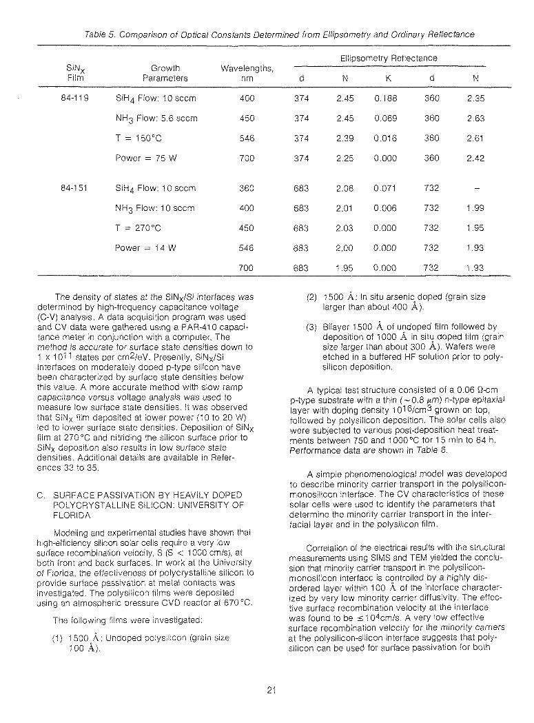
Table 5. Comparison of Optical Constants Determined from Ellipsometry and Ordinary Reflectance
Ellipsometry ReflectanceSiNx Growth Wavelengths,Film Parameters nm d N K d N
84-119 SiH4 Flow: 10 seem 400 374 2.45 0.188 360 2.35
NH3 Flow: 5.6 seem 450 374 2.45 0.069 360 2.63
T = 150°C 546 374 2.39 0.016 360 2.61
Power = 75 W 700 374 2.25 0.000 360 2.42
84-151 SiH4 Flow: 10 seem 360 683 2.06 0.071 732
NH3 Flow: 10 seem 400 683 2.01 0.006 732 1.99
T = 270°C 450 683 2.03 0.000 732 1.95
Power = 14 W 546 683 2.00 0.000 732 1.93
700 683 1.95 0.000 732 1.93
The density of states at the SiNx/Si interfaces wasdetermined by high-frequency capacitance voltage(C-V) analysis. A data acquisition program was usedand CV data were gathered using a PAR-41 a capacitance meter in conjunction with a computer. Themethod is accurate for surface state densities down to1 x 1011 states per cm2/eV. Presently, SiNx/Siinterfaces on moderately doped p-type silicon havebeen characterized by surface state densities belowthis value. A more accurate method with slow rampcapacitance versus voltage analysis was used tomeasure low surface state densities. It was observedthat SiN x film deposited at lower power (10 to 20 W)led to lower surface state densities. Deposition of SiNxfilm at 270 cC and nitriding the silicon surface prior toSiNx deposition also results in low surface statedensities. Additional details are available in References 33 to 35.
C. SURFACE PASSIVATION BY HEAVILY DOPEDPOLYCRYSTALLINE SILICON: UNIVERSITY OFFLORIDA
Modeling and experimental studies have shown thathigh-efficiency silicon solar cells require a very lowsurface recombination velocity, S (S < 1000 cm/s), atboth front and back surfaces. In work at the Universityof Florida, the effectiveness of polycrystalline silicon toprovide surface passivation at metal contacts wasinvestigated. The polysilicon films were depositedusing an atmospheric pressure CVD reactor at 670 cC.
The following films were investigated:
(1) 1500 : Undoped polysilicon (grain size100
21
(2) 1500 A: In situ arsenic doped (grain sizelarger than about 400 A).
(3) Bilayer 1500 A of undoped film followed bydeposition of 1000 A in situ doped film (grainsize larger than about 300 A). Wafers wereetched in a buffered HF solution prior to polysilicon deposition.
A typical test structure consisted of a 0.06 Q-emp-type substrate with a thin ( - 0.8 fJ-m) n-type epitaxiallayer with doping density 1016/cm3 grown on top,followed by polysilicon deposition. The solar cells alsowere subjected to various post-deposition heat treatments between 750 and 1000 cC for 15 min to 64 h.Performance data are shown in Table 6.
A simple phenomenological model was developedto describe minority carrier transport in the polysiliconmonosilicon interface. The CV characteristics of thesesolar cells were used to identify the parameters thatdetermine the minority carrier transport in the interfacial layer and in the polysilicon film.
Correlation of the electrical results with the structuralmeasurements using SIMS and TEM yielded the conclusion that minority carrier transport in the polysiliconmonosHicon interface is controlled by a highly disordered layer within 100 A of the interface characterized by very low minority carrier diffusivity. The effective surface recombination velocity at the interfacewas found to be ::; 104cm/s. A very low effectivesurface recombination velocity for the minority carriersat the polysilicon-silicon interface suggests that polysilicon can be used for surface passivation for both

Table 6. Summary of Measured Parameters of Solar Cells Without AR Coating (28°C)
Base Back Voe, Isc (> 0.6 p,m), L, S,Cell* Type Contact mV mA p,m cm/s
1P p ohmic 573 63.0 310-350
2P P BSF 574 64.0 310-350 4.2 x 10⁴ to 5 x 10⁴
5P P poly-Si 583 67.7 310-350 1100-1500BSF
1N n ohmic 566 62.7 190-250
2N n BSF 565 65.2 190-250 700-1000
5N n poly-Si 591 65.5 190-250 100-160BSF
* These cells have area A = 4 cm2 and thickness of about 210 ± 10 p,m except for cell 2N which was330 p,m thick. The results are averages obtained from 10 to 20 cells.
p- and n-type silicon. This suggestion is supported bythe following considerations:
(1) The minority carrier transport at the polysiliconmonosilicon interface, with no intentional insulating layer at the interface, is determined by thecarrier transport within the polysilicon, ratherthan by tunneling through the native insulatinglayer.
(2) The similarity of the electrical properties of thesolar cells with in situ doping, and the bilayerpolysilicon film, suggests a correlationbetween the electrical properties and themicrostructure in the polysilicon film.
(3) The observed lower dark current with polysilicon passivation compared to that without passivation can be explained by assuming theheavily doped interfacial layer must haveproperties significantly different from theproperties of the monosilicon. The dominantmechanism for low dark current with polysilicon is more sensitive to the arsenic dopantconcentration at the interface than to thecarrier concentration at the interface.
(4) The polysilicon-monosilicon interface acts as avery efficient barrier for minority carriers. Thisis mainly because of the very sudden transition from the orderly epitaxial single-crystallayer to the CVD-deposited polysilicon withrandomly oriented grains of a few hundredangstroms in size. Thus, the polysiliconmonosilicon interface can be regarded as aregion with a high degree of disorder. Such aheterojunction reduces recombination currentby forming quasi-blocking contacts.
22
The potential of heavily doped polysilicon toreplace the conventional high-low junction or BSF structure of silicon solar cells also was investigated. Theresulting solar cells showed improvements in red spectral response and moderate improvements in Voc whencompared with control cells made with the BSF structureor with back ohmic contact structures. To assess theorigin of these improvements, the effective surfacerecombination velocity, S, of the minority carriers in thepolysilicon was measured as they enter the polysiliconlayer. The measurements showed that S (polysiliconback) was less than S (BSF controls). This lowering of Sis the mechanism responsible for the improvement inVoc and red spectral response. Table 6 shows asummary of these results (References 36 to 38).
These results suggest a new class of silicon solarcell design that uses a thin base (:5 150 p,m) of 0.1 Q-cmresistivity p-type silicon contacted on the back byAl/Ti/Pd/Ag with a passivating layer of heavily dopedpolysilicon and a front surface passivated by oxide.This will attain high efficiency by reducing both frontand back surface recombination velocities. To furtherreduce S values, heavily doped polysilicon can beused to passivate the front metal contact areas.
D. INTERFACIAL BARRIERS: STANFORDUNIVERSITY
To study the nature of interfacial barriers in highefficiency silicon solar cells, XPS and BIS were usedto examine Si/Si02 and Si/SiNx interfaces. XPS allowsdeterminations of the bonding and valence banddensity of states, and BIS directly maps the conduction band density of states. Thus, XPS and BIS providecomplementary information-measuring states at andabove the Fermi level, respectively, in Si02 at theSi/Si02 interface.

XPS data on the Si/Si02 interface indicated thatthe interface is abrupt, and thermally grown oxides arechemically uniform beginning from 3 to 4 monolayersfrom the interface. It also was found that the strain inthe near interfacial region of Si02 does not causesignificant change in the nature of the Si-O bond.
BIS measurements showed that the conductionband for 13 A oxide looks very much like the siliconconduction band. With thicker oxides, electron charging problems occurred. Figures 10 and 11 show thevalence band by XPS and conduction band by BIS,respectively, for a 13 A Si02 film on a silicon (100)surface.
XPS measurements on SiNx samples also weremade. The SiNx films were deposited by plasmaenhanced CVD at the University of Washington andwere subsequently annealed in argon ambient at450°C for 40 min. It was observed that SiNx films hadoxidized and the film composition was more likeSiOxNy. Some films were depth profiled by angleresolved XPS and a gradient in nitrogen and oxygenconcentrations was detected.
The XPS results indicated that the film surfacewas enriched with oxygen and was depleted of nitrogen. The bonding configuration of silicon also wasobserved to be changed across the film and becomesmore like O-Si-O near the film surface, but it is likeN-Si-O in the bulk of the film (References 39 to 40).
E. MICROCRYSTALLINE SILICON HETEROJUNCTION: APPLIED SOLAR ENERGY CORP.AND BOSTON COLLEGE
This effort to enhance cell performance was toexplore the use of m-Si film on c-Si for solar cellapplications, either as a m-Si/c-Si heterojunction orm-Si as a window layer on c-Si p-n junctions. This wasdeemed possible because m-Si has an optical bandgap of 1.7 eV, and a crystal size of 100 A. Becauseof a good lattice match, m-Si could potentiallyenhance Voc by reducing interface recombinationvelocity. This program was a joint venture with BostonCollege using an evaporation scheme to depositdoped films of m-Si with in situ hydrogenation. TheApplied Solar Energy Corp. (ASEC) was to supply suitable substrates and also make solar cells after m-Sideposition. Evaporated films and solar cells were to becharacterized by both contractors.
Earlier experiments on non-silicon substrates haddemonstrated microcrystal sizes of about 100 A andan optical bandgap of 1.7 eV. The wavelengthdependence of the absorption coefficient data fore-beam evaporated layers closely matched dataobtained by glow discharge techniques. Work underthis contract was concentrated, therefore, on makingdifferent cell structures and their characterizations.Nearly 40 deposition runs were made, with substratetemperatures varying from 572 to 652°C, and layer
(j)IZ:::Jau>ex:<tex:IIJ)ex:<t
2.000 -
-
-
I-
I I I I I
$0" •..• 0... .
o .• • 0,.
o~
0, .o
• 0
oo •
'0
I I I
...
I
'10 •.. ;. "s-,"'" I." 0
f/iltI"l.-. ".. . .. "o
o
•.
I
-
-
-
-
-
-
-
-
-
-
-
-o
o ,
'.oo l...-__Il--_---1I__--l..I__--l..I__--l-__-l...__-'-__~I __J..-_·....;.u../~;.:..J•• rl:o-.....L·_~
1450 1475
0iII BINDING ENERGY, eV
Figure 10. Valence Band of 13 A Si02 Over Si [1 OOJ
23

3.000
(j)
I-Z::J0U
>- 2.000a:::<ta:::I-eoa:::<t
1.000o.
.G i&@ .0 €I
• e e, ... .." , .......~..
..e,oo. .
, .';) , oil ••
$&e.(lj$$ lit
1$ (J lIP Q$.,doG e& ••
e.e & 6..•
'0
KINETIC ENERGY,
Figure 11. Conduction Band of 13 A Si02 Over Si [100J
thicknesses varying from a few tens of angstroms toslightly less than 1 p,m. Each run yielded five coatedsubstrates, most of which were fabricated into cells.
The m-Si deposition system consisted of a vacuum chamber with an e-beam evaporation systemusing a graphite boat containing pure silicon. Boronand antimony as p- and n-type dopants could be coevaporated by electrical heating. Both substrateheating and in situ cleaning with hydrogen plasmawere provided. Hydrogen plasma also was used forin situ hydrogenation of the m-Si film either during orafter growth.
Heterojunction structure was affected by interfaceand shunting problems and the best Voc achieved wasonly 482 mV, well below that of single-erystal siliconhomojunctions. The heterojunction structure of p-mSi/p-n showed promise on some of the samples. Thecomplementary structure did not show any improvement. Although several runs with different depositionconditions were made, the results were inconsistent.Any Voc enhancement obtained was too small tocompensate for the current loss because of the extraabsorption and poor carrier transport properties of them-Si film. A study of the m-Si/c-Si interface using a p-por n-n heterojunction showed that m-Si did not alwaysserve as a minority carrier barrier as expected. TheVoc in many samples was of opposite polarity fromthat predicted which indicated some degree of carrier
24
collection. This raised problems concerning the natureof the m-Si/c-Si interface. Cell efficiencies varied from0.6 to 8.3 % at 100 mW/cm2 with AR coatings, signifyingpoor minority carrier lifetime and interface shunting.
The SIMS study revealed carbon along theinterface and within the layer. Replacement of thegraphite boat with a boron nitride boat reduced thecarbon content, but did not eliminate it. Copper andMo also were dicovered as contaminants. Photomicrographs showed uneven surfaces, bubbly areas, andetch pits, signifying poor quality of the film. For thisapproach to succeed, interface problems need to besolved, and quality of the deposited layer of m-Sineeds to be improved (Reference 41 ).
F. X-RAY PHOTOEMISSION SPECTROSCOPY: JETPROPULSION LABORATORY
High-resolution x-ray photoemission spectroscopywas used for chemical analyses of some of the SiNxfilms. These films were grown by PECVD at the ,JointCenter for Graduate Studies (JCGS) at 270°C (seeSection III. B. for details). Surface passivationcharacteristics of these layers were investigated bymeasuring density of states (Nss) using a high-frequencyCV technique. Nss values were measured in the range of109 to 1012 states/cm2.
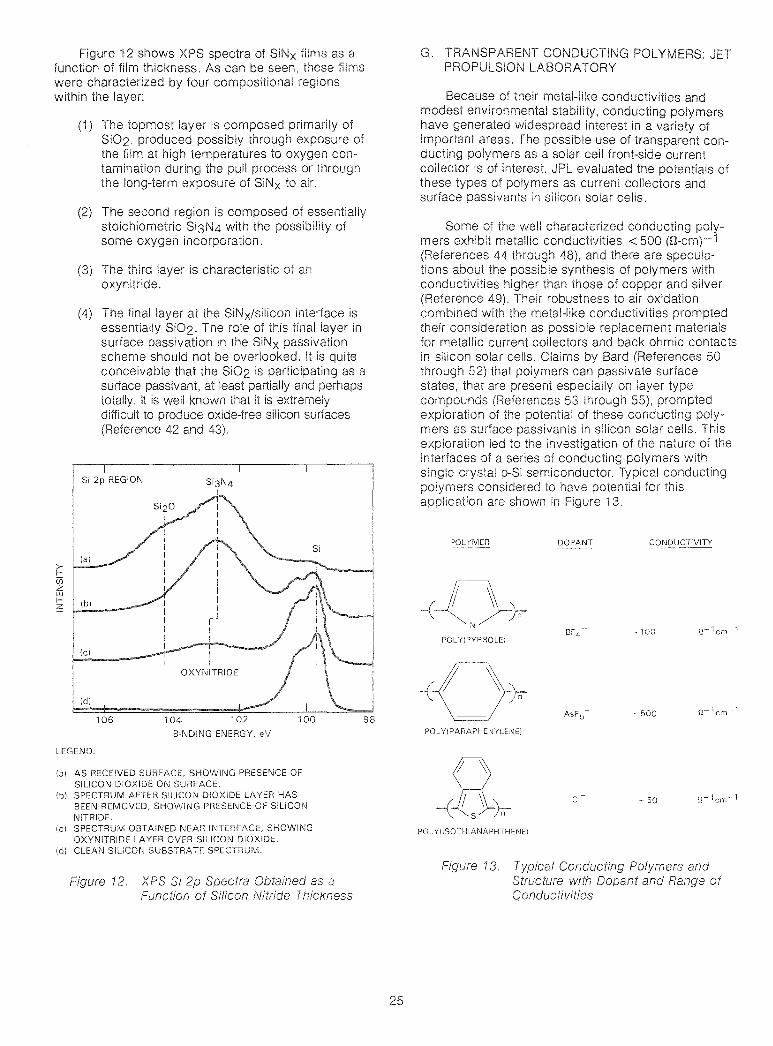
0- 1cm- 1
v~n .... w<e:· JET
CONDUCTIVITY
-500
-100
DOPANT
POLYIPARAPHENYLENEI
POLYMER
G. TRANSPARENT CONDUCTINGPROPULSION LABORATORY
Because of their metal-like conductivities andmodest environmental stability, conducting polymershave generated widespread Interest In a variety of
areas. The possible use of transparent conpolymers as a solar cell front-side current
collector is of Interest. JPL evaluated the potentials ofthese of polymers as current collectors andsurface passivants in silicon solar cells.
-<Dr,N
POLYIPYRROLE)
Some of the well characterized conducting polymers exhibit metallic conductivities < 500 (n-cm)-1(Re,ferenl::es 44 through 48), and there are C>1-":;;vL"CC
tions about the possible synthesis of polymers withconductivities than those of copper and siiver(Reference 49). Their robustness to air oxidationcombined with the metal-like conductivities promptedtheir consideration as possible replacement materialsfor metallic current collectors and back ohmic contactsin silicon solar cells. Claims by Bard (References 50thr''1l1r,h 52) that polymers can passivate surfacestates, that are present especially on layer
(References 53 55), nrArY'ln,tari
exploration of the of these conductingmers as surface in siiicon solar cells. Thisc.v,,,IArOlt'An led to the investigation of the nature of theinterfaces of a series of conducting polymers withsingle crystal p-Si semiconductor. Typical conductingnnl\ln'AI~C: considered to have potential for thisappii(~ation are shown Figure 13.
98100104 102
BINDING ENERGY, eV
106
(d)
(3) The third layer Is characteristic of anoxynitride.
(2) The second region Is composed of essentiallystoichiometric SI3N4 with the possibility ofsome oxygen incorporation.
II
OXYNITRIDE
The final layer at the SiNx/silicon interface isessentially S102. The role of this final insurface passivation in the SiNx passivationscheme should not be overlooked. It is quiteconceivable that the Si02 is participating as asurface passlvant, at least partially and perhapstotally. It is well known that it is avlrarnall\f
difficult to produce oxide-free silicon surfaces(Reference 42 and 43).
SI 2p REGION
(1) The topmost layer is composed primarily ofS102, produced possibly exposure ofthe film at high temperatures to oxygen contamination during the process or rnr,'1l1rm
the long-term exposure of SiNx to air.
Figure 12 shows XPS spectra of films as afunction of film thickness. As can be seen, these filmswere characterized by four compositional regionswithin the layer:
LEGEND:
(a) AS·RECEIVED SURFACE, SHOWING PRESENCE OFSILICON DIOXIDE ON SURFACE.
(bl SPECTRUM AFTER SILICON DIOXiDE LAYER HASBEEN REMOVED, SHOWING PRESENCE OF SiLICONNITRIDE.
(e) SPECTRUM OBTAiNED NEAR INTERFACE, SHOWINGOXYNITRIDE LAYER OVER SILICON DIOXIDE.
(d) CLEAN SILICON SUBSTRATE SPECTRUM.
POLYilSOTHIANAPHTHENE)
CI 50
Figure 12. XPS Si 2p Obtained as aFunction of Silicon Nitride Thickness
13. Conducting I"OIVn0Rf',c;
Structure with L/V/Jcu'"
Conductivities
25
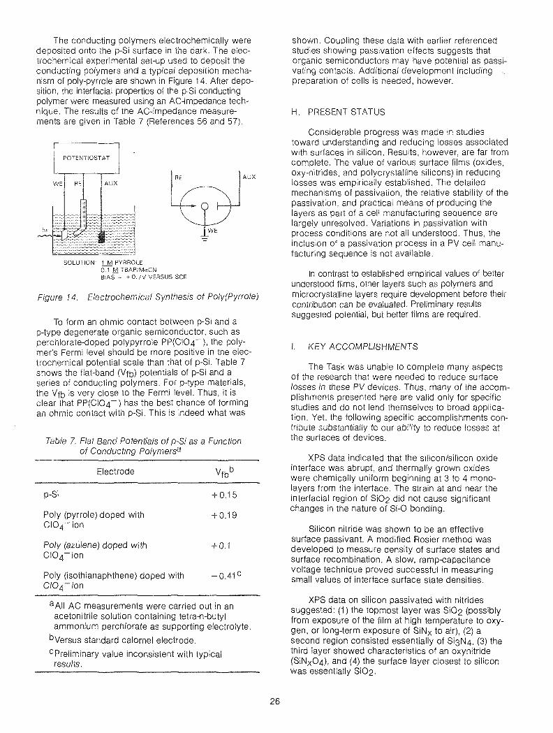
Figure 14. Electrochemical Synthesis of Poly(Pyrrolej
Table 7. Flat Band Potentials of p-Si as a Functionof Conducting Polymersa
I. KEY ACCOMPLISHMENTS
shown. Coupling these data with earlier referencedstudies showing passivation effects suggests thatorganic semiconductors may have potential as passivating contacts. Additional development includingpreparation of cells is needed, however.
H. PRESENT STATUS
Silicon nitride was shown to be an effectivesurface passivant. A modified Rosier method wasdeveloped to measure density of surface states andsurface recombination. A slow, ramp-capacitancevoltage technique proved successful in measuringsmall values of interface surface state densities.
The Task was unable to complete many aspectsof the research that were needed to reduce surfacelosses in these PV devices. Thus, many of the accomplishments presented here are valid only for specificstudies and do not lend themselves to broad application. Yet, the following specific accomplishments contribute substantially to our ability to reduce losses atthe surfaces of devices.
In contrast to established empirical values of betterunderstood films, other layers such as polymers andmicrocrystalline layers require development before theircontribution can be evaluated. Preliminary resultssuggested potential, but better films are required.
Considerable progress was made in studiestoward understanding and reducing losses associatedwith surfaces in silicon. Results, however, are far fromcomplete. The value of various surface films (oxides,oxy-nitrides, and polycrystalline silicons) in reducinglosses was empirically established. The detailedmechanisms of passivation, the relative stability of thepassivation, and practical means of producing thelayers as part of a cell manufacturing sequence arelargely unresolved. Variations in passivation withprocess conditions are not all understood. Thus, theinclusion of a passivation process in a PV cell manufacturing sequence is not available.
XPS data indicated that the silicon/silicon oxideinterface was abrupt, and thermafly grown oxideswere chemically uniform beginning at 3 to 4 monolayers from the interface. The strain at and near theinterfacial region of Si02 did not cause significantchanges in the nature of Si-O bonding.
AUX
+0.15
+0.19
+0.1
WE
RE
SOLUTION: 1 M PYRROLE5"1M TBAP/MeCNBIAS +O.7V VERSUS SCE
Electrode
p-Si
Poly (pyrrole) doped withCl04-ion
Poly (azulene) doped withCl04-ion
Poly (isothianaphthene) doped withCI04-ion
POTENTlOSTAT
WE RE AUX
~<--c:-:::=
hi'~
~
,..,..-.. ;::;;:~
~ ~
~
~
The conducting polymers electrochemically weredeposited onto the p-Si surface in the dark. The electrochemical experimental set-up used to deposit theconducting polymers and a typical deposition mechanism of poly-pyrrole are shown in Figure 14. After deposition, the interfacial properties of the p-Si conductingpolymer were measured using an AC-impedance technique. The results of the AC-impedance measurements are given in Table 7 (References 56 and 57).
To form an ohmic contact between p-Si and ap-type degenerate organic semiconductor, such asperchlorate-doped polypyrrole PP(CI04-), the polymer's Fermi level should be more positive in the electrochemical potential scale than that of p-Si. Table 7shows the flat-band (Vfb) potentials of p-Si and aseries of conducting polymers. For p-type materials,the Vfb is very close to the Fermi level. Thus, it isclear that PP(CI04-) has the best chance of formingan ohmic contact with p-Si. This is indeed what was
aA11 AC measurements were carried out in anacetonitrile solution containing tetra-n-butylammonium perchlorate as supporting electrolyte.
bVersus standard calomel electrode.
cPreliminary value inconsistent with typicalresults.
XPS data on silicon passivated with nitridessuggested: (1) the topmost layer was Si02 (possiblyfrom exposure of the film at high temperature to oxygen, or long-term exposure of SiNx to air), (2) asecond region consisted essentially of Si3N4, (3) thethird layer showed characteristics of an oxynitride(SiNx04), and (4) the surface layer closest to siliconwas essentially Si02.
26

A new silicon solar cell design was proposedhaving: (1) a thin base (> 150 J-tm) of 0.1 !J-cm p-typesilicon with a shallow (0.2 J-tm) junction, (2) contacts onthe back and front in selected areas with an intermediate to heavily doped polycrystalline silicon layer ofabout 1000 A thickness, (3) the remaining contactsurfaces passivated by growth of Si02 at 800 °C, and(4) a double layer AR coating used as in conventionalceils for better optical absorption.
Microcrystalline silicon deposition was done in ane-beam evaporation chamber with co-evaporation ofeither boron or antimony as p- or n-type dopant andin situ hydrogen passivation by a plasma generator topassivate m-Si bonds and obtain a higher bandgap of1.7 eV.
J. FUTURE NEEDS
Significant additional effort is needed in the application, understanding, and effectiveness of surfaceand interface passivation. It is clear that such effort isvaluable because of the significant gains in Voc to be
27
made using this approach. These efforts should be animportant part of continued R&D in the field of photovoltaics.
A. primary need is a detailed understanding of thechemical-structural bonding at the free silicon surfaceso that the impact of previous history, processingeffectiveness, and reliability can be controlled. Withthis understanding, the complex and sensitive passivation step can be reoptimized each time the design,process, material or process sequence is changed.
In addition to this general need for a better understanding of passivating layers, certain interestinglayers still require development for full evaluation oftheir potential. Microcrystalline silicon, although similarto polycrystalline layers, may hold some advantagesand could be further developed. The organic layers,because of low-temperature application, showpromise. Additional polymer material composition anddeposition developments are required before questions of optimum performance on solar cells andreliability can be addressed.

Devices
A. INTRODUCTION
This Task element addressed two main topics:(1) determination of the suitability of various preparedsilicon sheets produced by diverse technologies tomeet the FSA cost goals (conversion efficiency is a firstorder determinant of cost), and (2) novel approaches tothe achievement of very high (> 20 %) conversion efficiency in silicon solar cells. Both topics involvedinternal JPL research coupled with contractor support.
The major sheet technologies evaluated rangedfrom semicrystalline silicon to dendritic web. Baselinefabrication processes were established at ASEC andJPL, and were used to compare the competing sheetgrowth materials. Cell output data, coupled with morefundamental measurements such as minority carrierdiffusion length, were used to evaluate the progress ineach material and to compare them to each other andagainst single-crystal Cz silicon.
A great deal of processing and measurementwork was done on dendritic web material under a contract with Westinghouse. The advanced processes ofsurface passivation, multiple layer AR coatings, andback-surface reflectors were employed. Fundamentalmeasurement techniques of deep-level transient spectroscopy (DLTS), EBIC, and TEM were used to assessthe impact of growth parameter variations and postgrowth annealing on the minority carrier diffusion lengthof dendritic web. Cells were fabricated with conversionefficiencies of nearly 17%. Diffusion length improvements by more than a factor of three (to 120 j.tm) wereattained in optimized dendritic-web material.
Cell processing schemes to advance the performance of all devices were predicated on feedback fromthe FSA modeling effort. Modeling identified the majorloss mechanisms that limited the achievement of veryhigh efficiency for cells fabricated from single-crystalsilicon. Sophisticated solar cell designs were investigated aimed at reducing or eliminating the effect ofsurface recombination velocity and enhancing bulkcollection.
The two major cell configurations evaluated in thiswork were the floating emitter solar cell transistor andthe dot contact cell. The former cell was conceived byC.T. Sah and processed by ASEC. It aims at reducingthe deleterious effect of high-emitter doping by anapproach that allows the emitter to function effectivelyat a significantly lower doping concentration. This celldesign also should make surface passivation mucheasier and allow enhanced bulk collection efficiency.The dot contact cell design, investigated by JPL, seeksto reduce the effect of surface recombination by use of a
29
geometr~ featuri~9 small i~olated emitters separated bywell-paSSivated Silicon. ThiS reduces emitter recombination because of the reduced volume of the emitter.
Work on both cell designs ran into severeprocessing problems that prevented either approachfrom fulfilling its potential. The last processing runsdealing with the floating emitter cell, however, produced encouraging evidence that this design may becapable of achieving a greater than 20 % conversionefficiency. Current densities as high as 45 mA/cm2were obtained and showed that the enhanced currentcollection postulated for this type of solar cell is valid.Further progress with the dot contact cell, however,requires improvements in photolithography andsurface passivation techniques.
At JPL, an additional approach to obtain highefficiency silicon cells involved the use of high-qualityFZ silicon to fabricate cells. The FZ silicon wasprocessed with the most sophisticated conventionalfabrication processes such as shallow junctions,refined contact configurations, surface texturing, andmultiple AR coatings. It seems that the AR coatingprocess also acts to passivate the silicon surface.Using this approach, conversion efficiencies from18.6 to 22 % AMi (depending on cell size) have beenobtained.
A study at North Carolina State University was toevaluate: (1) use of the rapid thermal process (RTP) asa viable procedure to dissolve grown-in defects andnucleation sites for oxygen precipitation, and (2) therapid junction activation procedure following ionimplantation to prevent the occurrence of any subsequent defect nucleation or other lifetime-degradingprocesses. By dissolving grown-in defects and bypreventing them from occurring subsequently, one canimprove the minority carrier lifetime and thereby theefficiency. Studies continued to obtain optimum RTPand implant cycles with known precipitate denudedzones in the input material.
B. HIGH-EFFICIENCY CELLS PREPARED FROMWEB SILICON: WESTINGHOUSE
This research was directed toward improving bothsilicon web material and processing techniques toproduce high-efficiency cells (goal of 18 %). Westinghouse investigated the influence of twin planes,dislocations, trace impurities, and internal stress onbulk minority carrier lifetime. Processing investigationsincluded annealing effects, cleaning effect, surfacepassivation, AR coatings, and BSRs.
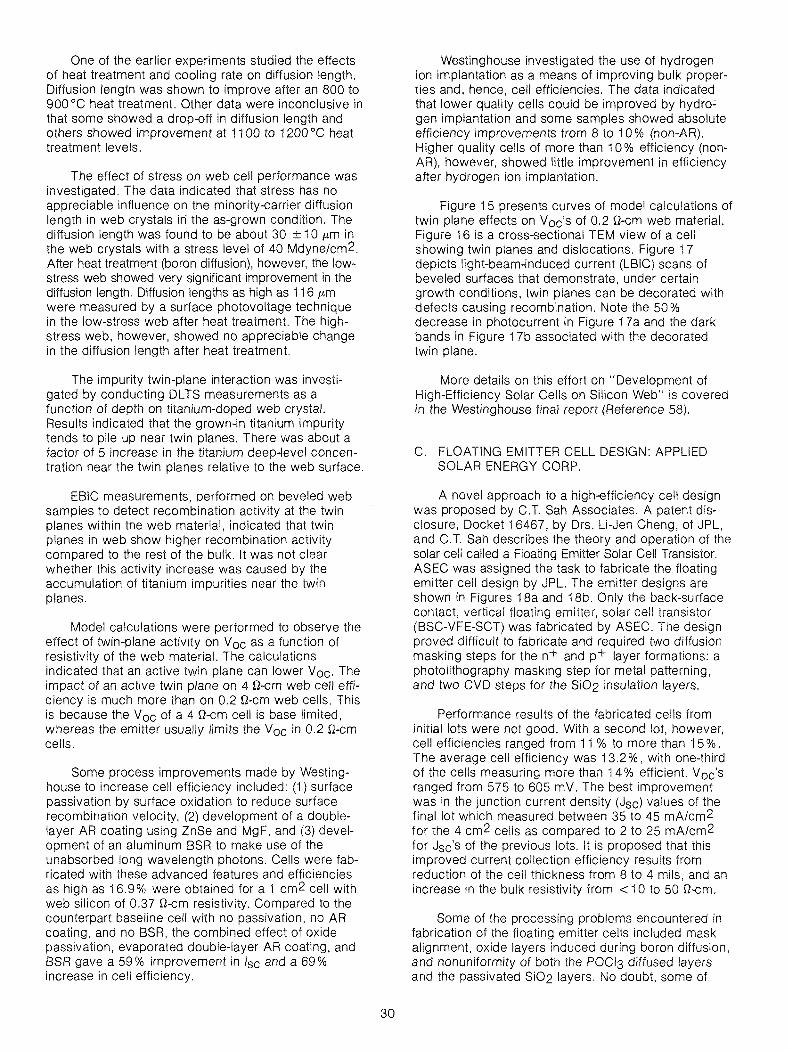
One of the earlier experiments studied the effectsof heat treatment and cooling rate on diffusion length.Diffusion length was shown to improve after an 800 to900°C heat treatment. Other data were inconclusive inthat some showed a drop-off in diffusion length andothers showed improvement at 1100 to 1200 °C heattreatment levels.
The effect of stress on web cell performance wasinvestigated. The data indicated that stress has noappreciable influence on the minority-carrier diffusionlength in web crystals in the as-grown condition. Thediffusion length was found to be about 30 ± 10 Jlm inthe web crystals with a stress level of 40 Mdyne/cm2.After heat treatment (boron diffusion), however, the lowstress web showed very significant improvement in thediffusion length. Diffusion lengths as high as 116 Jlmwere measured by a surface photovoltage techniquein the low-stress web after heat treatment. The highstress web, however, showed no appreciable changein the diffusion length after heat treatment.
The impurity twin-plane interaction was investigated by conducting DLTS measurements as afunction of depth on titanium-doped web crystal.Results indicated that the grown-in titanium impuritytends to pile up near twin planes. There was about afactor of 5 increase in the titanium deep-level concentration near the twin planes relative to the web surface.
EBIC measurements, performed on beveled websamples to detect recombination activity at the twinplanes within the web material, indicated that twinplanes in web show higher recombination activitycompared to the rest of the bulk. It was not clearwhether this activity increase was caused by theaccumulation of titanium impurities near the twinplanes.
Model calculations were performed to observe theeffect of twin-plane activity on Voc as a function ofresistivity of the web material. The calculationsindicated that an active twin plane can lower Voc . Theimpact of an active twin plane on 4 Q-cm web cell efficiency is much more than on 0.2 Q-cm web cells. Thisis because the Voc of a 4 Q-cm cell is base limited,whereas the emitter usually limits the Voc in 0.2 Q-cmcells.
Some process improvements made by Westinghouse to increase cell efficiency included: (1) surfacepassivation by surface oxidation to reduce surfacerecombination velocity, (2) development of a doublelayer AR coating using ZnSe and MgF, and (3) development of an aluminum BSR to make use of theunabsorbed long wavelength photons. Cells were fabricated with these advanced features and efficienciesas high as 16.9% were obtained for a 1 cm 2 cell withweb silicon of 0.37 Q-cm resistivity. Compared to thecounterpart baseline cell with no passivation, no ARcoating, and no BSR, the combined effect of oxidepassivation, evaporated double-layer AR coating, andBSR gave a 59 % improvement in Isc and a 69 %increase in cell efficiency.
30
Westinghouse investigated the use of hydrogenion implantation as a means of improving bulk properties and, hence, cell efficiencies. The data indicatedthat lower quality cells could be improved by hydro"gen implantation and some samples showed absoluteefficiency improvements from 8 to 10% (non-AR).Higher quality cells of more than 10% efficiency (nonAR), however, showed little improvement in efficiencyafter hydrogen ion implantation.
Figure 15 presents curves of model calculations oftwin plane effects on Voc's of 0.2 Q-cm web material.Figure 16 is a cross-sectional TEM view of a cellshowing twin planes and dislocations. Figure 17depicts light-beam-induced current (LBIC) scans ofbeveled surfaces that demonstrate, under certaingrowth conditions, twin planes can be decorated withdefects causing recombination. Note the 50 %decrease in photocurrent in Figure 17a and the darkbands in Figure 17b associated with the decoratedtwin plane.
More details on this effort on "Development ofHigh-Efficiency Solar Cells on Silicon Web" is coveredin the Westinghouse final report (Reference 58).
C. FLOATING EMITTER CELL DESIGN: APPLIEDSOLAR ENERGY CORP.
A novel approach to a high-efficiency cell designwas proposed by C.T. Sah Associates. A patent disclosure, Docket 16467, by Drs. Li-Jen Cheng, of JPL,and C.T. Sah describes the theory and operation of thesolar cell called a Floating Emitter Solar Cell Transistor.ASEC was assigned the task to fabricate the floatingemitter cell design by JPL. The emitter designs areshown in Figures 18a and 18b. Only the back-surfacecontact, vertical floating emitter, solar cell transistor(BSC-VFE-SCT) was fabricated by ASEC. The designproved difficult to fabricate and required two diffusionmasking steps for the n+ and p+ layer formations: aphotolithography masking step for metal patterning,and two CVD steps for the Si02 insulation layers.
Performance results of the fabricated cells frominitial lots were not good. With a second lot, however,cell efficiencies ranged from 11 % to more than 15%.The average cell efficiency was 13.2 %, with one-thirdof the cells measuring more than 14% efficient. Voc'sranged from 575 to 605 mV. The best improvementwas in the junction current density (Jsc) values of thefinal lot which measured between 35 to 45 mA/cm2for the 4 cm 2 cells as compared to 2 to 25 mA/cm2for Jsc's of the previous lots. It is proposed that thisimproved current collection efficiency results fromreduction of the cell thickness from 8 to 4 mils, and anincrease in the bulk resistivity from < 10 to 50 Q-cm.
Some of the processing problems encountered infabrication of the floating emitter cells included maskalignment, oxide layers induced during boron diffusion,and nonuniformity of both the POCI3 diffused layersand the passivated Si02 layers. No doubt, some of
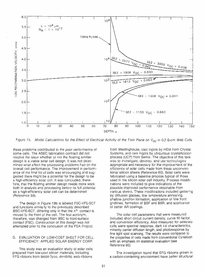
SE2 = 1208 Voe = 0.661
100 110 120 130 140 150
SE2 1155 Voe 0.662
SE2 = 1808 Voe
103
SE2 = 161 2 voe::=~0~.6~5~3~.#~===::=::===----l
1.5
1 .0 '::-_ ____'___~_ ___JI______'____l___ ___'___'___"_ _'___ __L___'___ __'___'___.l..__ __L_ ___I
o 10 20 30 40 50 60 80 90
DEPTH,1l
6.0
5.5 L = 104 Ilm
NA 1 x 10¹⁷
5.0 TWIN PLANE
(/)
E(,) 4.5
>--f-U0 4.0~
w>Z0 3.5i-«ziii~ 3.00uwa:Q 2.50~
2.0
Figure 15. Model Calculations for the Effect of Electrical Activity of the Twin Plane on Voc in 0.2 O-cm Web Cells
these problems contributed to the poor performance ofsome cells. The ASEC fabrication contract did notresolve the issue whether or not the floating emitterdesign is a viable solar cell design. It was not determined what effect the processing problems had on theoverall cell performance. The improvement in performance of the final lot of cells was encouraging and suggested there might be a potential for the design to bea high-efficiency solar cell. It was concluded, therefore, that the floating emitter design needs more workboth in analysis and processing before its full potentialas a high-efficiency solar cell can be determined(Reference 59).
The design in Figure 18b is labeled FSC-VFE-SCTand functions similarly to the previously describedBSC-VFE-SCT, differing only in that the n+ contact ismoved to the front of the cell. The first acronym,therefore, was changed from BSC to front-surfacecontact (FSC). Construction of this design was notattempted prior to the conclusion of the FSA Project.
D. EVALUATION OF LOW-COST SHEET FOR CELLEFFICIENCY: APPLIED SOLAR ENERGY CORP.
This study was an evaluation study of solar cellsprepared from low-eost silicon materials, includingEFG ribbons from Mobil-Tyco, dendritic web ribbons
from Westinghouse, cast ingots by HEM from CrystalSystems, and cast ingots by ubiquitous crystallizationprocess (UCP) from Semix. The objective of this taskwas to investigate, develop, and use technologiesappropriate and necessary for the improvement of theefficiency of solar cells made from these unconventional silicon sheets (Reference 60). Solar cells werefabricated using a baseline process typical of thoseused in the silicon solar cell industry. Process modifications were included to give indications of thepossible improved performance obtainable fromvarious sheets. These modifications included getteringby diffusion glasses, low temperature annealing,shallow junction formation, application of fine frontgridlines, formation of BSF and BSR, and applicationof better AR coatings.
The solar cell parameters that were measuredIncluded short circuit current density, curve fill factor,and conversion efficiency. Also measured for selectedcells were spectral response, dark I-V characteristics,minority carrier diffusion length, and photoresponse byfine light spot scanning. The results were compared tothe properties of cells made from conventional Cz-siliconwith an emphasis on statistical evaluation (seeReference 60).
The investigation found that EFG ribbons grown ina carbon-eontaining environment have better structural
31
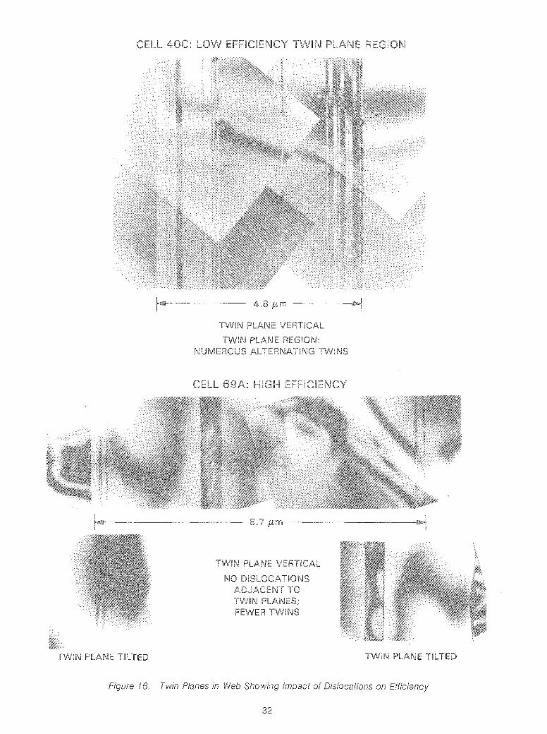
CI N
4.8 m ----
~-------
NS
Figure 16. Twin Planes in Web S/'J,()WInO
32
of Dislocations on tmclei7CV

Figure 17. LBIC Scans of Beveled Sample Prepared from Cell 17C (9.5%
(a) (b)
18. Floating Emitter Solar Cell Transistor
perfection, such as large less dislocation4<:"''011"\1 and carrier diffusion Solar cellsmade from these specific EFG ribbons haveefficiencies in with cells mF'OFlrArl fromearlier EFG ribbons. The best cell achieved
the advanced process was about 14 % .
33
The evaluation of web ribbons suggested that webcells made using the baseline process have efficiencies
lower than those made of Cz silicon. Celi per-formance agreed with the of dislocation densities
the ribbons.
The baseline processing capability consisted offorming an junction in p-type materialphosphorus at 850°C from a phosphine source for20 min. This yielded a junction between 0.35 and0.4 /hm. Spreading resistance measurements indicatedthat the surface concentration was 5 x 1 9 atoms/cm3.A metal tri-Iayer back contact of titanium, palladium, andsilver then was evaporated on the back of the cell andsintered at 600°C in hydrogen to form an ohmic contact.The front contacts were formed by evaporating titanium,palladium, and silver a shadow mask. The laststep was to evaporate 625 of Ta20S on the front asan AR coating. The basic process flow is illustrated in
9. A detailed description of JPL's baselineprocessing is described in Reference 62.
F. HIGH-EFFiCIENCY CELL PROCESSING:JET PROPULSION LABORATORY
To increase the short wavelength (blue) responseof the cells and decrease emitter recombination, thediffusion process was altered so that the junction depthwas reduced to 0.2 /hm and the surface concentrationwas lowered to 1 xi 019 atoms/cm3. To accomplishthis, the diffusion temperature was lowered to 800°C.The diffusion time was retained at 20 min.
In 1984, a major effort was initiated tosolar cells that would be comparable to the best cellsavailable at that time. This required several changes tothe baseline process. FZ wafers were purchased withrespective resistivities of .0 to 2.0, 0.3 to 0.5, and0.15 to 0.25 O-cm. FZ wafers were used because theirlow oxygen content results In fewer defects and longerminority carrier diffusion lengths. This was especiallyimportant for iower resistivity materials. FZ materialalso would maintain its lifetime during thermal cyclingcaused cell processing.
The JPL FSA was involved in theprocessing of silicon solar cells from 1980 to 1986.The solar cell processing capability was initiated toevaluate silicon sheet materials that weredeveloped by various FSA Project contractors. Thefacility also was used to basic research onimproving cell performance.
To improve the back contact, 2000 A of aluminumwere added as the first layer for the back contact.When sintered at 500°C for 20 min in hydrogen, a
doped p+ contact was formed at the back.This resulted in a small increase in voltage and moreconsistent curve factors (Reference 63).
E. RAPID THERMAL PROCESSING: NORTHCAROLINA STATE UNIVERSITY
It should be emphasized that the results reportedhere represent the somewhat immature state of develr.n,-nQ!nt (1981) for these forms of silicon. No systematiccomparisons of quality and performance have beenmade since 1981 .
The evaluation of cells made of material hadnr",hlcrY)C' both of reproducibility from run to run,
,nif,nrn,itll of sheet within an Junc-tion which could be caused by particulateinclusions observed in the was a result ofthese and low-temperature
Imrwr.,/c cell performance.
The evaluation of UCP cells prepared the base-line process suggested that the quality of this siliconmaterial was lower than that of Cz silicon. Overall ceilnA,"fr.,·m"nr·"" was relatively uniform with the exception
a few cells that showed shunting problems causedparticulate inclusion.
The objective of this study was to evaluate rapidthermal processing (RTP) as a viable procedure for:(1) Cz substrate modification using high-temperature dissolution treatments, and (2) rapid junction activation following ion implantation. The reason for the first treatment is to dissolve grown-in defects and nucleationsites for oxygen precipitation. The second treatmentshould be done as quickly as possible (e.g., < 10 s) toprevent the occurrence of any subsequent defectnucleation or lifetime-degrading processes.
The experimental approach for substrate evaluation used preferential chemical etching and x-raytopography to delineate defects which then are corre-lated with carrier lifetime. The x-ray delinea-tion is enhanced by a lithium decoration procedure performed at temperatures less than 450°C both prior toand after a high temperature dissolution anneal. Siliconwafers examined have been as-grown as well as furnaceand RTP annealed with various combinations of 1200,1050, and 750 °C thermal cycles.
Initial generation lifetime (Gg) maps did correlateGg with defects delineated by x-ray topography. Theraw data, obtained from samples with and without aRTP of 1200 °C for 1 min prior to a 1100 °C/80-minfield oxide-growth, showed a significant improvementwith the RTP treatment (10 /hs without, and 35 /hS withan RTP cycle).
Results show that correlation between processinduced defects and values for Gg spans a range from100 to 1000 /hS, and recombination is generally afactor of 10 lower. Studies also were included toobtain optimum RTP and implant cycles with knownprecipitate-denuded zones as Input materials(Reference 61).
To achieve a further increase in current, it wasnecessary to improve on the single-layer AR coating.A single-layer coating produces about a 40 % increasein current compared to the uncoated cell value. Adouble-layer AR coating, by comparison, theoreticallywould result in up to a 56 % increase in current.a double-layer AR coating consisting of TiOx and
34
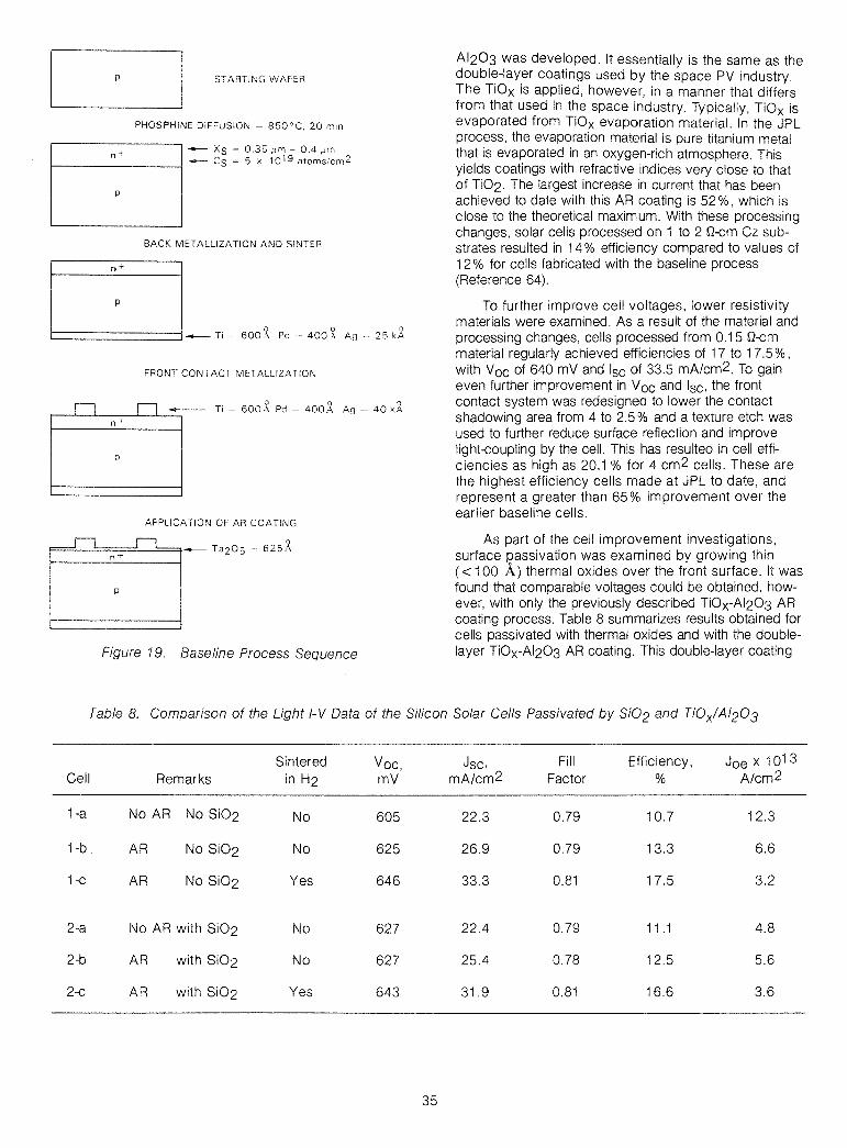
'-- p J...J STARTING WAFER
PHOSPHINE DIFFUSION - 850°C, 20 min
n+ -XS=0.35I'm-OAl'mf---------I- Cs = 5 x 10¹⁹ atoms/cm 2
p
BACK METALUZATION AND SINTER
p
t=======j 0 0 0___ Ti - 600A Pd 400A Ag - 25 kA
FRONT CO NTACT METALLIZATION
II II - Ti - 600~ Pd - 400 X Ag - 40 kZn T
p
APPLICATION OF AR COATING
p
Figure 19. Baseline Process Sequence
AI203 was developed, It essentially is the same as thedouble-layer coatings used by the space PV industry.The TiOx is applied, however, in a manner that differsfrom that used in the space industry. Typically, TiOx isevaporated from TiOx evaporation material. In the JPLprocess, the evaporation material is pure titanium metalthat is evaporated in an oxygen-rich atmosphere. Thisyields coatings with refractive indices very close to thatof Ti02. The largest increase in current that has beenachieved to date with this AR coating is 52 %, which isclose to the theoretical maximum. With these processingchanges, solar cells processed on 1 to 2 {l·cm Cz substrates resulted in 14 % efficiency compared to values of12% for cells fabricated with the baseline process(Reference 64).
To further improve cell voltages, lower resistivitymaterials were examined. As a result of the material andprocessing changes, cells processed from 0.15 Q-cmmaterial regularly achieved efficiencies of 17 to 17.5%,with Voc of 640 mV and Isc of 33.5 mA/cm2. To gaineven further improvement in Voc and Isc , the frontcontact system was redesigned to lower the contactshadowing area from 4 to 2.5 % and a texture etch wasused to further reduce surface reflection and improvelight-coupling by the cell. This has resulted in cell efficiencies as high as 20.1 % for 4 cm 2 cells. These arethe highest efficiency cells made at JPL to date, andrepresent a greater than 65 % improvement over theearlier baseline cells.
As part of the cell improvement investigations,surface passivation was examined by growing thin« 100 A) thermal oxides over the front surface. It wasfound that comparable voltages could be obtained, however, with only the previously described TiOx-A1203 ARcoating process. Table 8 summarizes results obtained forcells passivated with thermal oxides and with the doublelayer TiOx-A1203 AR coating. This double-layer coating
Table 8. Comparison of the Light I-V Data of the Silicon Solar Cells Passivated by Si02 and TiOx/A1203
8intered Voc , Jsc , Fill Efficiency, Joe x 1013
Cell Remarks in H2 mV mA/cm2 Factor % A/cm 2
1-a No AR No 8i02 No 605 22.3 0.79 10.7 12.3
1-b. AR No 8i02 No 625 26.9 0.79 13,3 6.6
1-c AR No 8i02 Yes 646 33.3 0.81 17.5 3.2
2-a No AR with 8i02 No 627 22.4 0.79 11 .1 4.8
2-b AR with 8i02 No 627 25.4 0.78 12.5 5.6
2-c AR with 8i02 Yes 643 31.9 0.81 16.6 3.6
35

technique has three advantages over the thermal oxidepassivation technique: (1) the high-temperature thermaloxide process, which can adversely affect overall cellperformance, is eliminated; (2) two process steps can becombined into one, simplifying overall processing; and(3) optical absorption losses are reduced by eliminatingthe oxide layer.
In 1984, SERI awarded a contract to JPL todevelop dot junction silicon solar cells. The basicconcept was that open-circuit voltage could beincreased by reducing the emitter contribution to thereverse saturation current. It was proposed that thiscould be accomplished by limiting the total junctionarea. To achieve this, the n+ diffusion was limited tosmall areas or "dots" on the surface of the cell. Theindividual junctions were then interconnected by ametal contact grid. A model was developed in parallelwith the processing work. Results of the model analyses are shown in Figure 20 (References 65 and 66).
As shown in Figure 20, Voc increases as the ratioof junction to total cell area is reduced. Unfortunately,there is a simultaneous drop in current caused by theloss of photogenerated carriers before they can becollected at the junction. This indicates the bulkdiffusion length would have to be much greater thanthe distance between the dots, and the surfacebetween the dots must be very well passivated toobtain the full potential of this solar cell. Reduction ofthe dot spacing leads to problems with photolithography and increased metal coverage. A summary ofsolar cells made from FZ and Cz materials is shown inTable 9. The data corroborate the model as Voc isincreased for cells with reduced junction areas whencompared with cells that have junctions covering theentire surface. There also is a decrease in lsc for cellswith reduced junction areas.
680 35
C'JE"::0(
> EE 660 30 ~
"-,
0 >-'> "-"- I-ui "- iii(:J ..... ....- z« /'<.. u.JI- ....- ...... 0--J
640 ....- ...... 25 I-a / ...... Z> ...... u.JI- - ...... a:S ...... a:..... :::JU ...... u9': ......u .................. l-
SZ Uu.J 620 20 a:"-a __ Lb ~ 300~m U
I---- Lb ~ 100 ~m a:
aI(j)
60020 50 100
DOT JUNCTION DIA. d, ~m
18 I I I
-*>-' 16- -
u ------zu.J
U ,.... ................ ...-u:u- ....-u.J
,////....---J14 '- ---J
u.JU ,/ --Lb 300 ~m
---Lb 100 I'm
12 I I I
20 25 50 75 100
DOT JUNCTION DIA, d, I'm
Figure 20. Calculated Solar Cell Parameters for DotJunctions with 100-f1.m Separation
Table 9. Dot Junction Solar-Cell Results and Corresponding Efficiency
Cell Voc , Jsc , Fill Efficiency,b Junction/AreaCell Configurationa mV mA Factor % Ratio, %
036-1-1 282-50 585 30.5 0.568 10.24 2.5
036-1-2 594 31.5 0.554 10.37 2.5
036-1-3 590 30.9 0.580 10.57 2.5
036-0-4 597 31.4 0,588 11.02 2.5
036-2-1 141-50 585 28.9 0.689 11.66 10.0
036-2-2 548 29.0 0.565 8.97 10,0
036-2-3 531 29.8 0.561 8.87 10.0
036-2-4 577 29.4 0.679 11.53 10.0
a Refer to dot separation S and dot diameter d in microns, respectively, for 282-50, etc.
bCells are 2 x 2 cm on 1 to 2 Q-em FZ substrates. Measurements made at 25°C and 100 mW/cm2.
36

G. PRESENT STATUS
Based on results to date, it seems there are severalviable approaches to achieve a 20% conversion efficiency for silicon solar cells. It also is apparent thatsophisticated processing will be required and that workmust be continued to reduce these processes to practice. Once this has been accomplished, both the dot contact and floating emitter concepts should be revisited.The use of both thinner and lower resistivity materialshould be emphasized in any future work. A morethorough understanding of the mechanism associatedwith the passivating property of certain AR coatings isrequired to fully exploit this process in ad,'anced cellconcept fabrication schemes. Dendritic web has beendemonstrated to be the sheet material with the greatestpotential for high efficiency with low cost.
The achievement of laboratory solar cell efficiencies of 20% in FZ silicon and 16.9 % in dendritic websuggests that 22 % conversion efficiency for silicon isa realistic goal. The progress made in significantlyincreasing the minority carrier diffusion length indendritic web is even more reason for optimism withrespect to this sheet material. Proven processescapable of a major reduction in surface recombinationvelocity, coupled with the high-current densitiesachieved by the floating emitter cell, are additionalpositive signs that silicon can meet the objectivesneeded for low-cost terrestrial power generation.
High-temperature thermal treatments to dissolvegrown-in defects and oxygen-precipitating nucleationsites were employed to prevent the occurrence of subsequent defect nucleation or lifetime-degrading processes.
An advanced solar cell laboratory was establishedat JPL and was used to evaluate various types ofsheet silicon as well as to produce advanced solarcells. Devices with AM1 efficiency > 20 % wereproduced and several advanced individual processsteps were developed. Similar studies directed atspecific goals were conducted by several contractorsincluding Westinghouse (web-dendrite) and ASEC(various sheets and floating emitter cells).
The efforts in this sub-task, although complete andsuccessful in themselves, are of types that are nevercompleted. Not only does the quality of the base siliconsheet continue to change with time, but new processsteps and concepts are developed and new cell designsare proposed and proven. The interplay of all of thesefactors produces a multi-dimensional array of possiblehigh-efficiency approaches. Although modeling andunderstanding greatly reduce the number of choices tobe explored, the remaining number is still substantial.
H. KEY ACCOMPLISHMENTS
Key accomplishments are:
(1) Specific cell processes and designs for solarcells made of dendritic web silicon were conceived, developed, and applied. Web cell efficiency of 16.9% was achieved.
37
(2) A unique floating emitter cell design was evaluated. Although its proposed advantages werenot proven, initial results were encouraging.
(3) The performance of a variety of unusual silicon sheets was evaluated and comparedusing baseline methods. Improvement in efficiency in these sheet cell efficiencies afteroptimized cell processing was determined.
(4) Rapid temperature processes have beenevaluated and are promising for dissolvinggrown-in defects and nucleation sites, foroxygen precipitation, and for rapid junctionactuation following ion implantation.
(5) A combined dOUble-layer AR coating with surface passivating properties was developed.
(6) State-of-the-art solar cell facilities wereestablished at JPL to evaluate cells made fromvarious sheet materials on an ongoing basis.These facilities ultimately produced a 20 %(AM1) 4 cm 2 cell using FZ silicon.
(7) A dot contact cell was proposed and developed.Several experimental limitations, however,prevented evaluation of its full potential.
I. FUTURE NEEDS
Future needs consist of:
(1) Periodic reassessments of the performancecapabilities of unusual silicon sheets with costpotential for terrestrial photovoltaics.
(2) Assessment of advances and new concepts incontrol of minority carrier losses. This includesbulk passivation, surface passivation, andcontact passivation.
(3) Development and proof-of-concept of processsequences that incorporate old and newindividual steps. This will lead to continualadvances in the demonstrated efficiency ofcrystalline silicon photovoltaics. Specialattention should be paid to the impact ofchoice of specific types of silicon sheet.
(4) Continual evaluation of the interplay betweensheet quality and characteristics, solar celldesigns, and process steps and sequences.
(5) Development of new cell designs that havebecome possible through better control oflosses. Methods to control metal contactlosses, for example, would permit designers toconsider different contact configurations.

n
A. NTRODUCTION
To explore means to the theoretical limitof silicon solar cell many cell designs needto be and analyses tounderstand the cells' Because ov,",orl'YH",nt,,1
evaluation of innumerable alternatives is not nr~ll"'tll"'",1
the chosen approach is evaluationnumerical For the numerical model to beaccurate, the physics of the device should be correctlyrepresented, the relationships ofdesign parameters should be correctly accountedand the data to the numerical model should beaccurate. Because the evaluation results obtainedthe modeling approach are as accurate as thedata used as to the model, the correct measurement of the data used in the model is as important asthe model itself. The research effort under this sub-task dealing with wasdirected toward both the establishment of an accuratenumerical analysis model for cell-design evaluationand the improvement of the measurement tOl'hn,f"1i
used to acquire reliable data.
A state-of-the-art silicon solar cell performanceevaluation model was available in the public domainand was procured and made functional at JPL. Thismodel (Solar Cell Program in One Dimension(SCAPi D) from Purdue was used as aprimary tool in the evaluation of several new designconcepts and in the performance of sensitivityanalyses. The in-house research effort at JPL hasresulted in several reports with hiah-E~ffic;iejlCV
silicon solar cell designs, in identification of keyparameters the cell and in "'''''1<:::ltl\l;j"\/
analysis.
When the numerical model is used extensively,the computer cost of the techniquebecomes an important issue in cost effectiveness ofthis approach. A research effort at Research TriangleInstitute was directed toward deveiopment of acomprehensive silicon solar cell evaluation modei inone dimension with an emphasis on making thecomputer program use less central processing unit(CPU) run-time. RTI used a novel solution technique toachieve the objective of a decreased use of the CPU.
The simulation models mentioned above areuseful in evaiuating the of a cell with agiven design. The program has to be run repeatedlywith each and every variation of the design data set toperform sensitivity analysis. There is no mechanism tooptimally modify the design parameters to obtain abest design. A brute force method of evaluating allpermutations and combinations of many parameterswould be prohibitively expensive. A research effort atUCLA was directed toward developing a code to
39
op1:im,,,lly vary the design simultaneouslyand suggest a best design. The code developed atUCLA serves as a front end to a numerical simulationmodel. The code uses the simulationmodel as a tool for evaluating the impact of parametervariations and then automatically modifiesthe until the best design isidentified.
The two input parameters to the abovesimulation and optimization models are: (1) minoritycarrier lifetime, and (2) recombination velocities at thefront and back surfaces. These parameters dlri9Ctlivaffect the recombination losses occurring at variousregions of the cell, namely, at the front surface,emitter, and at the back surface.research efforts, directed toward development of newand improved techniques of measurement of theseand related parameters, are described below.
The research effort at the University of Floridawas directed toward developing measurement techniques that accurately measured recombination invarious regions of the cell. Although the measurementof recombination properties is difficult, it is importantto the understanding of the factors that uitimately limitsilicon solar cell performance.
A research effort at University of SouthernCalifornia expiored the applicability of laser-calorimetric spectroscopy to study deep-level impur-ities in silicon. These in turn, will affect the
carrier lifetime diffusion length). Theadvantage of this method is that it is free from electricfield effects such as those used in photoconductivitystudies. When the spectroscopic measurements weremade, difficulty was encountered in obtaining resultsfor the high-resistivity samples doped with a deep-levellIillJlllliV of a simple level structure, such asSi:Au.
Research was carried out at the University ofPennsylvania to identify, develop, and analyze usefultechniques to measure both bulk recombination ratesin all regions and surface recombination velocities ofhigh-efficiency silicon solar cells. Two methods havebeen identified of selective measurement in multiplelayers. One method, Absolute Spectral Light BeamInduced Current (ASLBIC), measures spectral responseat selected wavelengths, specifically short wavelengths.Another method, Modulated Light Measurementmeasures the phase shift of currents induced by twomodulated light beams each with a different wavelength(penetration depths).
Research efforts at JPL in the area of devicemeasurements included: (1) EBIC characterization ofsolar cells using a chopped scanning electron microscope beam, (2) EBIC measurements of minority

C. OPTIMIZATION METHODS FOR SOLAR CELLNUMERICAL MODELS: UNIVERSITY OF
LOS ANGELES
The objective function of the program is to maximize the solar cell efficiency. The decision variablesconsidered are: cell thickness, front junction depth,back depth, front surface doping concentra-
bulk and back surface concentration.
A copy of the SICELL program was received atJPL and was successfully installed on the GPVAXcomputer system.
this method shares similarities with someaspects of NI methods, it differs markedly in otheras~)ecits Abbreviated forms of analytical relationships,representing the solution of solar cell transport equations obtained using this new method, are presented inthe final RTI report (Reference 67). Also discussed inthis report are: (1) similarities and differences betweenthe NI and the new methods, (2) recently reported phenomenological submodels that are used in the newsimulation program, (3) other phenomena submodelsthat have been developed in this program, and (4) theoperating characteristics of the simulation program thatare results obtained from simulations. Validation studies included in this report show the simulation accuracy is in the range of 0.08 to 3.6% for 27experimental data points over the temperature rangeof 300 to 421 K.
mobilities and dependencyon (3) band-to-band Auger,assisted Auger, and SRH recombination processes;
oxide-charged insulated surface layers; (5) built-inelectric fieids under non-equilibrium injection levels;and solar concentrations and nondegenerateand degenerate contributions to the absorption curve.
The grid point separation is determined.Saturation and depletion region current contributionsto dark current are used to determine the equivalentsaturation current and diode exponential factor fromwhich the equivalent diode relationship is obtained. Asubtraction method is used to obtain the spectralresponse. Short-circuit currents are determined usingthe full spectrum and one in which the flux is centeredabout any wavelength, (Ao). The latter is subtractedfrom the full spectrum. The difference between the twoIsc's is used to obtain the spectral response at AO'This may be repeated for as many Ao's as required.
The efforts at UCLA were directed towarddeveloping a comprehensive silicon solar cell designopltimization model and a companion computer program. Using SCAP1 D as a basic tool for evaluating theno,rfnl'rn"nr'", of a given solar cell design, an attemptwas made to develop an optimization code in whichthe parameters are varied simultaneously in annn·tlm::;i fashion. The best design is suggested theprogram for the given technology limited parameterslike bulk lifetimes and surface recombination velocities
and
CPU-EFFICIENT DEVICE MODELING CODE:RESEARCH TRIANGLE INSTITUTE
All the above studies are described in greaterdetail in the sections discussing theindividual research activities.
SICELL is a one-dimensional silicon solar cellanalysis program. A model was developed thatdescribes the distribution that establishes a built-infield. The method may be used to calculate built-infields in generalized cases. Other salient features ofthis program are as follows: Boltzmann and Fletcher
relationships are corrected to account forthe net charge distribution in quasi-neutral regions.Phenomena submodeis that are incorporated in thesimulation program include: (1) lattice, ionized
and carrier-carrier scattering contributions to
This effort concentrated on development of a"Comprehensive Silicon Solar Cell Code."The was to develop a computer code thatwould be less expensive to run with a set ofdata for a silicon solar cell, compared to that ofconventional models that use numerical int,,,.,r,,tir,n
methods to solve the differential equations thatrepresent the device. In this study, a new method wasdeveloped that has been used to simulate thecharacteristcs of semiconductor devices.
In this new method, the set of transport equationsis to each mesh point, and (through a judiciousselection of mesh-point distribution) a relativelyaccurate closed-form analytical solution is obtained atthe assigned mesh of theconditions to an n-mesh point field results in
'-""1uallVI'u that require simultaneous solution. Thissolution is manifested the determination of the2n-constants of integration where each closed-formQnilltirm r<'nr<~Q",ntirH' a mesh contains twoconstants of . A solar cell transport solutionis represented by the complete set of constantsobtained in the nand p regions. As a result, thecomplete set of closed-form functions describes thebehavior of the photoexcited carrier concentrations fora continuum of x values in the nand p regions. Theph()toex(:;itE~d carrier relationships are used to obtainthe current-voltage relationship from which are deter-
the maximum power point and conversion efficiency. Effects of temperature, solar concentrationphenomena, submodel parameters, and structureparameters may be studied using this program as atool. This program is named SICELL.
carrier recombination the emitter and at thefront surfaces, and (3) measurement of carrierlifetime in siiicon sheets. A sensitive microwavereflection measuring system was and built at
PL. Work included efforts to formulate an adequatean,ily;:::is method to extract quantitative results fromexperimental data on photoconductive decay. Thiswould allow an estimation of carrier lifetimeand surface recombination velocity.
40

CEL~ OSCILLOSCOPE
-'f-
~r-
-
I;-' Rt = 0 ~
--
itO)
/,/'
SLOPE ex Td
o
If-----I
LOGei(t)
En and Seff (technique described in Section II.E.)to obtain the emitter component (Je).
(2) Je is a function of Dp/Neff and Tp, where Dpand Tp are the minority carrier diffusivity andlifetime, respectively, and Neff is the effectivecarrier density after accounting for heavydoping effects.
v
(a)
(3) Values of Dp/Neff and Tp are now available(see Section II.F.). Literature values of Dprepresent the primary uncertainty in thismeasurement.
An improved Isc decay technique was developedto measure both the recombination time in the baseregion of silicon solar cell samples and the back surface recombination velocity. The improved techniquewas called the ESCCD method. Figure 21 shows aschematic diagram of the measuring circuitry of theESCCD technique (Reference 68). The techniquesimultaneously measures the carrier lifetime in the bulkof the cell and the recombination velocity at the backinterface with the contact. With this method, a forwardbias is applied to the solar cell to set up a steady-statecondition. Then, by rapidly applying a zero bias acrossan extremely small resistance, a short circuit isobtained. This causes the pin junction region and thebase and emitter regions to discharge. If the dischargetimes related to the junction and emitter regions aremuch smaller than the time related to the base region,the lifetime and recombination velocity can bedetermined.
D. MEASUREMENT OF RECOMBINATION LIFETIMEAND SURFACE RECOMBINATION VELOCITY:UNIVERSITY OF FLORIDA
Given the values for SF, SB, and T, the program willautomatically determine the optimal values for theseparameters.
The emitter profile options considered by theoptimization program are the complementary errorfunction, a step function, and a parabola. Consideration of a gaussian profile and defining the profile pointby-point could also be included. The possibility ofvarying the objective function suitably, so that theprogram automatically would decide the designparameters for achieving a cell efficiency of a givenvalue, was explored but not completed. The othervariation of the objective function that was consideredwas the identification of the parameter values forseries resistance, etc., to match the experimental I-Vcurve of an experimental design. The preliminaryresults of this effort are very promising.
According to the University of Florida, one of themain advantages of this technique is that the dischargetime of the pin junction (on the order of 10-11 s) ismuch less than the discharge times associated witheither the emitter or the base. This makes it very easyto interpret the observed transient current. The ESCCDmethod is simple, fast, and less expensive than othermethods used to measure other key solar cellparameters.
(bl
Figure 21. (a) Electronic Circuit Used in the SCCDMethod, (b) Schematic Illustration of theCurrent Decay Displayed on a Log Scale
In the final phase of this study, work was done onthe elusive task of measurement of front surfacerecombination velocity (Sp) in the thin highly dopedemitter region. A method was successfully demonstrated on small area n-p-n transistors. The approachincluded the following steps:
(1) Obtain the reverse saturation current (Jo) fromthe dark I-V characteristics. Deduct the basecomponent (Jb), obtained after measurement of
E. CRYOGENIC LASER CALORIMETRY FORIMPURITY ANALYSIS: UNIVERSITY OFSOUTHERN CALIFORNIA
A program was conducted at USC to determinethe applicability of laser-calorimetric spectroscopy tothe study of deep-level impurities in silicon. Therewere three parts to the effort: (1) to investigate criticalconsiderations in the application of calorimetric methodsto deep-level spectroscopy, (2) to design and build a
41

cryogenic calorimeter for measurements,and (3) to carry out calorimetric measurements ofabsorption in silicon.
The motivation for using calorimetry is its demonstrated high sensitivity that allows measurement ofrelative absorption as small as ten per million.Cryogenic operation was chosen to control thermalionization of the deep impurity levels, and to measurethe dependence of level energy. An additional advantage of calorimetry is freedom from electric field effects such as those present in photoconductivity studies.
The primary consideration for successfulabsorption spectroscopy of deep-level impurities isthat deep-impurity absorption dominates all otheroptical absorption mechanisms. Possible sources ofbackground absorption include free carrier absorption,absorption by precipitates and inclusions, two photonband-to-band absorption (pulsed sources only), andmultiple-phonon band-to-band absorption. The requirement of low free-carrier absorption is especially important; fundamental studies of deep-level impurities arerestricted to high-resistivity silicon. The impurity levelenergy is determined by measuring the photoabsorption cross section as a function of photon energy, andthen fitting the data using a line-shape model. Becauseof coupling to the lattice, the level energy cannot beaccurately determined merely by measuring the upperpart of the absorption shoulder. It is necessary tofollow the curve down as low as possible in the steepregion near the threshold energy.
The primary apparatus considerations were foundto be optical scattering, and the requirement of atunable continuous wave (CW) near-IR laser source.Optical scattering causes erroneous heating signalsand scattering is especially troublesome at ('(\./()('IPni('
temperatures because of the formation of frost on thesample if there is any residual water vapor. It also wasfound that Raman-shifted radiation from a Q-switchedNd:YAG laser resulted in an undesirable intensitydependence of the optical absorption. Consequently,CW laser sources are preferable. Efforts were concluded when it was realized that major experimentalproblems remained.
F. LOSS MEASUREMENT IN HEAVILY DOPEDEMITTERS: UNIVERSITY OF PENNSYLVANIA
Research efforts were conducted to identify,develop, and analyze useful techniques to measurebulk recombination rates, surface recombination rates,and surface recombination velocities in all regions of ahigh-efficiency solar cell. Of the two methods identifiedfor measuring selectively in multiple layers, ASLBICmeasures spectral response at selected wavelengths(primarily at very short wavelengths), and MLM measures the phase shift of currents induced by two ACmodulated light beams with different wavelengths(penetration depths). Both techniques require computer analysis using modeled cell structures and
42
",,,,r)::>r,::>t,,,I\/ measured distributions.",n,'p::>filnn resistance measurements are ::>n,~I\!:7Pri toprovide the doping distribution data.
The ASLBIC does not produce aanswer. Rather, the best answer is determined fromthe uniqueness of diffusion . surface loss pairsthat the spectral data. The thinness of most deviceemitters limits the usable 22 is anexample of a contour plot of the root-mean-square (rms)error of the fit to the data for a specific example for awide range of lifetime and surface recombination velocitypairs. The thinness of the emitter limited the useful wave-lengths to 350, 375, and 400 with absorption coeffi-cients of .65 x 106, 0.68 x 1 and 8.2 x 1 ,respectively. To prepare Figure 22, roughly 80 Individualcomputer runs were necessary. This research addressedthe areas of refinement and automation of the DCmeasurement of and the theoretical evaluationof measurements in complex device structures.
ASLBIC measurements require ultravioletspecifically in shallow emitters of current
cell designs. To improve measurement accuracy, thesystem was equipped with interference filters to trans-mit the various lines of the mercury (Hg)source for higher spectral This producedrepeatability of the measurement of better than half ofone percent. Software was implemented to completelysample the parameter space of the unknown withnumerous sand 7 pairs. The results are displayedthree-dimensionally showing the regions of good fit ofthe model to the experimental data. Also, a Simplexminimization was available to find the best fitnumerically (Reference 69).
G. DEVICE MODELING: JET PROPULSIONLABORATORY
New ideas of silicon solar cell designs and theirpotential for improved performance can easily beevaluated by an accurate computer simulation model.Compared to an experimental approach, analyticalevaluation techniques can quickly and cost-effectivelyevaluate many scenarios. Parametric analysis andsensitivity analysis studies are effectively performedby computer simulation.
A Solar-Gell Efficiency Estimation Methodology andAnalysis (SEEMA) scheme was established at JPL. Itused an existing state-of-the-art silicon solar cell performance evaluation model, SCAP1 D. This program wasavailable in the public domain and was procured andinstalled on the UNIVAC 1180-F computer system atJPL.
Under the SEEMA scheme, the performance of agiven silicon solar cell design was evaluated using theSCAPi D program as the basic tool. The one-dimensionalprocess simulation program SUPREM-II formed thebasic tool for simulating processes such as diffusion,etc. These analytical tools were used independentlyand/or in combination for cell design evaluation andsensitivity analysis studies.
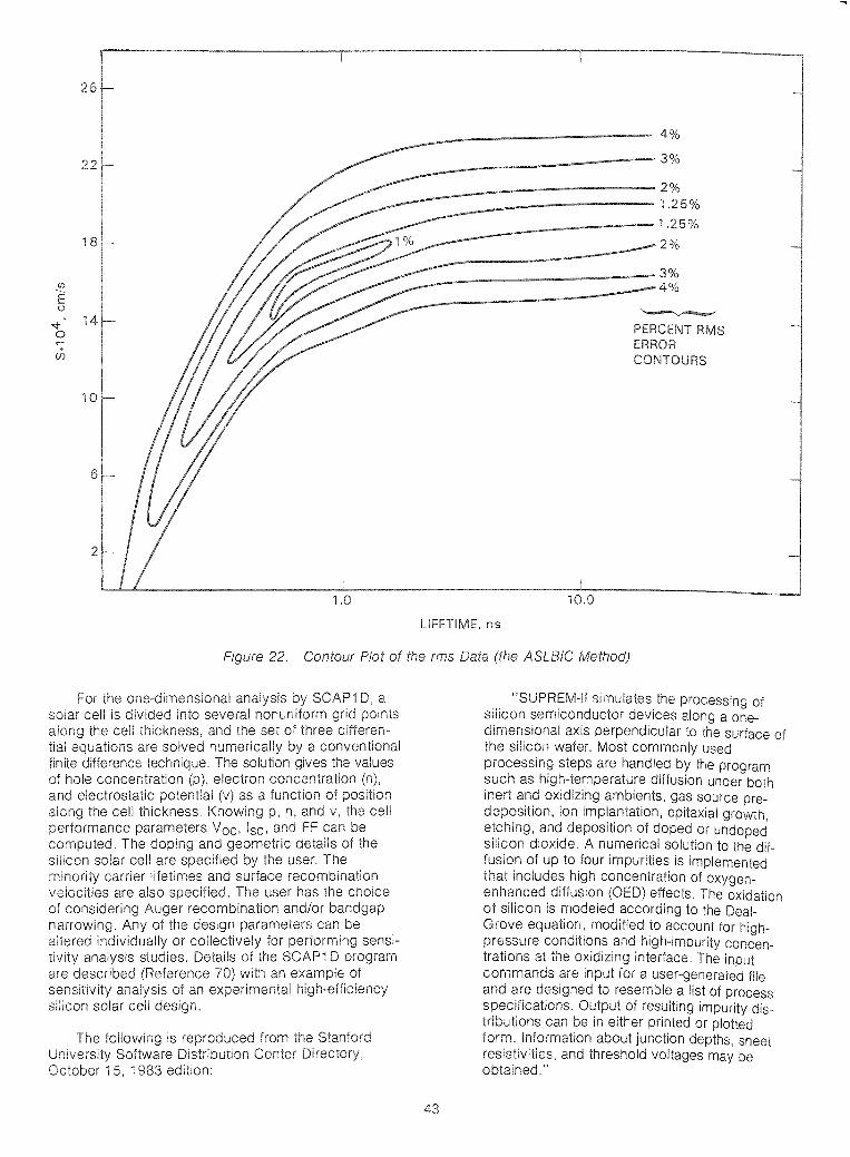
10.01.0
2
26
4%
22 3%
2%1.25%.25%
18 2%
3%(/) 4%Eu
~
'<t 14PERCENT RMS0
':" ERROR(j) CONTOURS
10
6
LIFETIME, ns
Figure 22. Contour Plot of the rms Data (the ASLBIC Method)
For the one-dimensional SCAP1 D, asolar cell is divided into several nonuniform pointsalong the cell thickness, and the set of three differen-tial equations are solved numerically a conventionalfinite difference technique. The solution gives the valuesof hole concentration electron concentrationand electrostatic potential as a function of positionalong the cell thickness. Knowing p, n, and v, the cellperformance parameters Voc, Isc, and FF can becomputed. The doping and geometric details of thesilicon solar cell are specified by the user. Therni""rihl carrier lifetimes and surface recombinationvelocities are also specified. The user has the choiceof considering Auger recombination and/or bandgapnarrowing. Any of the design parameters can bealtered individually or collectively for performing sensi-
analysis studies. Detaiis of the SCAP1 D programare described (Reference 70) with an example ofsensitivity analysis of an experimental high-efficiencysilicon solar cell design.
The following is reproduced from the StanfordInilll'>r'~it\1 Software Distribution Center Directory,
October 15, 1983 edition:
"SUPREM-II simulates the processing ofsilicon semiconductor devices along a onedimensional axis perpendicular to the surface ofthe silicon wafer. Most commonly usedprocessing steps are handled by the programsuch as high-temperature diffusion under bothinert and oxidizing ambients, gas source predeposition, ion implantation, epitaxial growth,etching, and deposition of doped or undopedsilicon dioxide. A numerical solution to the diffusion of up to four impurities is implementedthat includes high concentration of oxygenenhanced diffusion (OED) effects. The oxidationof silicon is modeled according to the DealGrove equation, modified to account for highpressure conditions and high-impurity concentrations at the oxidizing interface. The inputcommands are input for a user-generated fileand are designed to resemble a list of processspecifications. Output of resulting impurity distributions can be in either printed or plottedform. Information about junction depths, sheetresistivities, and threshold voltages may beobtained."
43

of such is the confirmationof the SUbsequent to this
the models then can effectively be used todetermine the effect of parametric variation on device
To compare model prediction withan experimental high-efficiency cell design
was considered with a measured efficiency of 18.7 % ,under illumination of 100 mW/cm2 at 28°C as published in the literature (Reference 71). It was shownthat SCAP1 D analysis results agree with thePYI'lpr'im,pnt",1 results.
I
'te191-I
:to
LIFETIME. 05
20 I
1
300
CELL THICKNESS. "m
Figure 24, Sensitivity of Efficiency of Solar-CellThickness for Various Minority CarrierLifetime Values
15 I20 50
16
;:;,en::iIIlVIIV analyses were performed with respectfront-surface recombination velocity,
m""1n,'ltll carrier lifetime, cell thickness, and back surface fieid. Results of the analysis indicate that with thebest possible combination of parameter values for SF,T, and cell thickness, the maximum efficiencyacill8VRiliA is about 20 %, It may be noted that then;:'I';:,n"1",t",no are varied one at a time. True optimization
C;\..i\JII c;;:, simultaneous improvement of all parameters
Additional study was performed to investigate theimpact of practical barriers such as heavy dopingeffects, Auger recombination, band-gap narrowing,surface recombination, and shadowing on highefficiency silicon solar cell performance, An idealcase, considering only radiative recombination lossesand technology limited and fundamentallosses, is evaluated to be around 29 %. This is comr;p"",hlp to the detailed balance limit maximum effi-
of a p-n junction solar cell of 30 %, estimatedShockley and Queisser (Reference 73). The heavy
and realizable values of SF and SB andshadowing, are considered in succession and theirinfluence on reducing the cell efficiency is evaluatedand is shown that these practical barrierscause the cell efficiency to fall to the experimentallyachieved value of 19 to 20 %. Improvement in Voc is
CJU<JII c;u to achieve cell efficiency greater than 20 %.Increase in value of lifetime reduces reverse saturationcurrent and hence improves Voc. The impact of practicalbarriers is shown schematically in Figure 25, The effectsof and SB is shown in Figure 26. These
indicate that cell efficiency greater than 20 %i CJUUII co;-, SF and SB to be reduced to 100 cm/s, and T
to be increased to 250 Ils. Other results of this researchare available (References 74 through 77).
SI0 2
TI Pd Agp+ POLYSILICON
Schematic Cross-Section of a PassivatedThin Silicon Solar Cell
p iO,Hl-eml
Innn\!,~h"", cell features then wereinc:oqJOr'atE~d in this cell to further reduce losses. Theschematic of this is shown in Figure 23. Bulkrecombination losses are reduced the cellthin (100 A BSR for the optical absorp-
iosses caused cell thinness. Both surfacesand are considered to be passivated by a silicondioxide to reduce surface recombination \/al,"""'"front and surface back (SB).HP,"nrnhin",ri"n losses under the contact are reduced
between the
new cell is shown to be capable of",,,r,ie,,,·;nrt 20 % ceil with achievabie
SF = SB = 000 cm/s and T = 20 Ils.shows of cell as acell thickness with carrier lifetime
For cell greater20%, substantial reduction in SF and SB and con-
c:irlprph!a lifetime are essential.state-of-the-art is
these values. Details of thisnr,::,,::;pnt,::,rl elsewhere Reference 72).
ELECTRON-BEAM INDUCED CURRENTCHARACTERIZATION OF SOLAR CELLS: JETPROPULSiON LABORATORY
The EBIC technique has been widely used tomeasure lattice defect distribution and transport"cr,!">",rlic,C' of semiconductors. An in-house researchtask at JPL this to measure the EBIC
as a function of distance from the junction withbeam incident on a cieaved (111) surface
of silicon solar cells 78), The results haveshown that the effective recombination velocity of the
44

(7)
28
T == 20 p.S
';fZ 260
>-'UZwUu::u..w
24....I....IWUII<{....I0(I)z 220u....I(I)
AUGER nt:\~urVIIJII\lf-\
B BANDGAP NARROWING
SF == FRONT SURFACE RE(:OrIllBINAVELOCITY
SB BACK SURFACE nt:\~UrVIIJII\lP,
VELOCITY
20
'"u..Z '" u.. '" Eu.. '"
°E OE OEz () 2000 00'"
II() II
() ()
112 112EcoO coO 11O 11O()
II II co II co II co II co IIu..co u..co Zco Zco Zco Z0(1) 0(1) ov, 0(1) ov, 0
II II IIII II
II II IIII
II
u.. u.. u.. u.. u..<{(I) <{(I) <{v, <{(I) <{v, <{
A B C 0 E
Figure 25. Impact of Practical Barriers on Silicon Cell Performance
EASUREMENTS OFRECOMBINATION: JETLABORATORY
An In-house research programout to the of the use of EBIC mea-surements to recombination nh,"nr,,,,,,,,n,;:
hA;::lIlIIIl-linr)Arl emitter andefficiency silicon solar cells. it has beenthis is suited to the investiqa1tioremitter and Even themental EBIC data were collected under three-dimensional has been shownsolution obtained with one-dimensional numericalmr,r1olinr is the EBIC data ancilvs:is
Bare oxide-coveredfaces were measured and rr.;mn"rc,rl
Good was obtainedfactor of 0.89 was assumed, thus sU1:::jqE3stinaabout 11 % of the carriers recombinedthe ceil This result Is similarlished data of silicon diodes with very shallowtions. The i"",..,rn\l""Y>o,..,t
emitter surface was covered withcan oxide was found to be about 27 %
cell with a 0.35
1,",,,,1_1'"11(11'"1 II mr'tlrm fr,r"",nn the BSF of silicon solarin addition to the diffusion and the surfacerecombination velocity of the surface no,-rlonrlirl
both the p-n and low-high can be deter-mined from the data provided a single EBIC scan.The measured value of the surface recombinationvelocity in the samples with AI-paste alloy back contacts always was found to be smaller than those ofsamples with evaporated AI contacts. This obser-vation agrees well with a known fact from solar cellfabrication that the BSF cells with AI-paste con-tacts are better than those with evaporated AIcontacts. This study provides an tool tostudy the BSF.
A related study for the BSF was conducted at JPLin cooperation with the University of Florida. The firstexperimental determination and interpretation of thevoltage across a high-low junction was obtained as afunction of the voltage across a nearby hlr,h_Ir.IAI
tion (Reference 79). Several n+ /p/p+ solar cells weremeasured. Figure 27 shows the typical voltageas a function of the applied voltage. Theoretical analysisshowed agreement with these experimental results. Atest structure also was proposed for the measurement ofthe effective surface recombination velocity at thelow junction.

23
----
SHADOWING INCLUDES;R REFLECTION LOSSES0
>-- 22uzw SF = FRONT SURFACEU RECOMBINATIONLLLL VELOCITYw...J...J
21 SB = BACK SURFACEu.Ju
RECOMBINATIONa::<r: VELOCITY...J0UJZ0u
20:J(jj
19
(j)(j)
E(j) E u (j)
;REu 0 ;RE ·0·
;Ro ;Ro ;Ro ,#o(j)o u~2 ~2
o u~2<::to 1'0 1'0----
~EII II II II II II II
II II II II uII
SCD SCD SeD SCD SCD SCDOUJ OUJ OUJ OUJ OUJ OUJ0 II 0 II 0 II 0
II 0 II ~ II<r: <r: <r: <r: <r:ILL ILL ILL ILL ILL IlLUJUJ UJUJ UJUJ UJUJ UJUJ UJUJ
A-l A-2 A-3 B-1 B-2 8-3
Figure 26. Impact of Shadowing and Surface Recombination Velocities on Silicon Solar Cell Performance
J. MINORITY CARRIER LIFETIME IN SILICONSHEETS: JET PROPULSION LABORATORY
Figure 27. High-Low Junction Voltage (measured)Versus Cell Applied Voltage
surface photovoitage method, suffers from experimentallimitations. To develop a better method to characterizethe minority carrier lifetime in silicon wafers and ribbons,in-house research has been carried out to study theapplicability of microwave reflectance measurements tomonitor the photoconductive decay in silicon wafers andribbons. From the measured photoconductive decay, onecan extract the information of carrier lifetime andsurface recombination velocity (Reference 81).
A highly sensitive microwave reflectancemeasuring system with computer data acquisition hasbeen designed and built at JPL. The experimentalresults illustrate that the microwave te:>"hnim
accurately can probe the decay of photogeneratedminority carriers in silicon sheet materials. This decaydepends on the carrier lifetime and surfacerecombination velocity. Under controlled surfaceconditions, one can measure bulk carrierlifetime in silicon sheets. With known lifetime in thebulk, the technique has been demonstrated to be aneffective tool for monitoring the surface recombinationvelocity. Preliminary results reveal that Cz and FZ silicon wafers have small surface recombination veloci-ties when they are etched In a dilutefluoric acid solution, but the recombination velocity
100 200 300 400
CELL APPLIED VOLTAGE. mV
250 r--,-----,---,--,---,---,---,-----,..------.>E
8 2000:::>(f)
;'5 150~
>UJ 100c:J«f-
6 50>~+0.
The measurement of minority carrier lifetime in silicon sheet materials, such as wafers and ribbons, is veryimportant for the characterization of silicon materials forPV applications. A commonly used method, that measures the m'lnority carrier diffusion length by using the
46

when the surface is toh"'("\n~"'''' saturated after several
inrrVY1nL",t", at this time to anClU''='lj,.,dtC "'n",I\/<::li'" method to extract qu;:mtitative
",vr,,,,rim,:::>nt,,,1 data.
, and made functional at JPL. Severalh'f"1h,.t:,ttlf'IOI'('\! siiicon solar cell designs andrnr1(;p,ntc:: have been evaluated and results
Improvements of all models are neededconsideration of new phenomeno
logical relationships.
The optimization model should be used forother simulation models for both solar cellsand for different materials like arsenideor silicon.
EBIC techniques were shown to be effectivetools to investigate courier recombinationparameters in the bulk and at the interfaces.
Considerable progress was made in thecation of the scanning laser-beam inducedcurrent (SLBIC) technique to measure diffusionlength in heavily doped emitter regions.
The RTI computer program, designed to savecomputer needs to be evaluated. If thiscode is a similar two-dimensionalcode should be developed.
novel numerical analysis code in oned with emphasis on economy incomputer time used per run, has been devel-
for the of sili-con solar cell of a
An improved Isc decay method was developedthat simultaneously was able to measure carrierlifetime in the bulk of a cell and recombinationvelocity at the back interface.
(3) An optimization code has been asa front end to the simulation model tothe parameters until a best
is identified.
(1) Basic modeling should be upgraded to use atwo-dimensional numerical modelsuch as SCAP2D. This requires modificationsto provide more efficient computer utilization.
M. FUTURE NEEDS
The tnlllnlA.linn items have been identified for futurework:
Two methods, the ASLBIC the MLMhave been identified research efforts at
the of to measure bulk recom-bination rates and surface recombination velocities.
In the research, a one-dimensionalnumerical analysis model was considered to be ade-
to evaluate the performance of a siiiconsolar cell design for use in solar arraymodules. A state-of-the-art numerical ",n""I1""<::available the domain, was used sUi::;cE~ssfully
in many silicon solar celldesigns. A an efficientcomputer code with on minimum "nmr\l,t,:::>rtime per run was butthe efficiency of the code was not proven. Anothereffort developed an code to be used as afront end of a simulation model to the
parameters until the best designis identified.
research efforts were directed toward thedevelopment of methods, techniques, or procedures tomeasure directly or the two key param-eters: the carrier lifetime (a measure ofrecombination losses in all regions of the cell) andsurface recombination velocities at the front and backsurfaces. Measurement at theJnl\JAr:l'itv of Florida better values for minnlrihl
effective surface recombination\loln,,'t\l at the back and the n,rm_'A\A. " In,,t,,,,,
behavior in a BSF cell. One theelectronic Isc decay had special interestbecause it measures the recombinationlifetime the base and the back surface recombina-tion \/OIA"'h.
K. PRESENT STATUS
KEY ACCOMPLISHMENTS
In the area of in-house researchstudies include: (1) EBIC characterization of solar cells
a electron beam,EBIC measurements of carrier recombina-
tion in the emitter and at the front surface, andstudy of of microwave reflectance
measurements to monitor the photoconductive decayin silicon wafers and ribbons to extract carrierlifetime and surface recombination velocity.
FoIIOlNlniO is a summary of ",r,,,nITInlid,montco'
(1) A state-01·-tnE)-artanalysis model
(5) Measurement techniques for key input datavalues should be emphasized, especiallythose related to minority carrier lifetime.
47

SECTION VI
Overview Status
As a result of studies and support from the HighEfficiency Device Research Task, major advanceswere made in all aspects of solar cell science.Because many efforts were terminated before completion much significant work remains to be done. Duringthe active years of this Task, the conversion efficiencyof crystalline-silicon solar cells advanced significantlywith final devices exhibiting efficiencies greater than22 % (AM1). Although this Task cannot claim directcredit for all of this progress, many of the advancescan be traced to its activities. Major accomplishmentsand unfinished work are summarized below.
A. KEY ACCOMPLISHMENTS
Following is a summary of accomplishments:
(1) Modeling techniques for solar cells weredeveloped and proved effective for evaluationof devices.
(2) New high-efficiency solar cells were conceived, modeled, and evaluated.
(3) New techniques were developed to measuresimultaneously minority carrier lifetime andsurface recombination velocity.
(4) Key barriers to obtain high-efficiency cellswere identified and, in many cases, reduced.
B. ADDITIONAL RESEARCH NEEDED
Although much understanding and improvement incrystalline-silicon solar cells has been accomplishedbecause of the research in this Task, the work is far
49
from completed as noted in the Summary section ofthis report. The general nature and sources of lossmechanisms are known. What is not known is theirdetailed response to processing and their variationfrom changes in silicon sheet type, especially low-eostvarieties of sheet. The studies in this Task were veryactive at the time of termination of the FSA Projectand, in many cases, need to be completed. After completion of the FSA Project, continued U.S. Departmentof Energy (DOE) support for research addressing alimited number of these problems is anticipated.
Specifically needed are:
(1) Determination of the remaining low-cost,silicon-sheet recombination mechanisms inbulk, in all layers, and at all surfaces.
(2) Establishment of quantitative relationshipsbetween defects and recombinationmechanisms.
(3) Development of new device structures andtheir verification using device modeling andexperiment.
(4) Establishment of correlations among materialdefects, device fabrication steps, and deviceperformance.
(5) Characterization of defects in silicon sheets astheir quality improves.
(6) Development of cost-effective and reliablepassivation techniques for bulk and surfacerecombination sites in appropriate forms ofsilicon sheet.

For acquisition of DOE/JPL documents listedbelow, see Appendix A.
. Sah, C.T, "Recombination Phenomena in HighEfficiency Silicon Solar Cells," Proceedings of theFlat-Plate Solar Array Project Research Forum onHigh-Efficiency Crystalline Silicon Solar Cells,DOE/JPL-1012-103, p. 37, 1985.
2. Sah, CT, "High-Efficiency Crystalline Silicon SolarCells," Solar Cells, October 1985.
3. Corbett, J.W, "Oxygen-and Carbon-Related Defectsin Silicon," Final Report of Contract, DOE/JPL956989-86/01, State University of New York atAlbany, 1986.
4. Wang, P.W, and Corbett, J.W, "Studies of OxygenThermal Donor Formation Under Stress," Proceedings of Symposium on Oxygen, Carbon, Hydrogen,and Nitrogen in Crystalline Silicon, Vol. 59, p. 167,Materials Research Society, Pittsburgh,Pennsylvania, 1986.
5. Borenstein, J.T., and Corbett, J.W, "A UnifiedTreatment of the Thermal Donor Hierarchies in Silicon and Germanium," Proceedings of Symposiumon Oxygen, Carbon, Hydrogen, and Nitrogen inCrystalline Silicon, Vol. 59, p. 159, MaterialsResearch Society, Pittsburgh, Pennsylvania, 1986.
6. Borenstein, JT, Peak, D., and Corbett, J.W,"Formation Kinetics of Thermal Donors in Silicon,"Proceedings of Symposium on Oxygen, Carbon,Hydrogen, and Nitrogen in Crystalline Silicon,Vol. 59, p. 173, Materials Research Society,Pittsburgh, Pennsylvania, 1986.
7. Goesele, U., and Ast, D.G., Carbon, Oxygen, andTheir Interaction with Intrinsic Point Defects inSolar Silicon Ribbon Materials, Annual Report,DOE/JPL-956046-83/9, 1983.
8. Sullivan, T, and Ast, D.G., EBIC Investigation ofHydrogenation of Crystal Defects in EFG SolarSilicon Ribbons, Quarterly Report,DOE/JPL-956046-83/5, 1983.
9. Ast, D.G., Electrical, Structural and ChemicalCharacterization of Silicon Sheet Material, AnnualReport, DOE/JPL-956046/86-1 , 1986.
10. Gleichmann, R., Vaudin, MD., and Ast, D.G.,"Interactions of Twin Boundaries and Dislocationsin Solar Silicon," Phil. Mag. Vol. A, pp. 51,449,1985 (also topical technical report,DOE/JPL-956046-84/10).
51
n
11. Ast, D.G., The Structure of < 110> TiltBoundaries In Large Area Solar Silicon, AnnualReport, DOE/JPL-956046-82/5, 1982 .
12. Lindholm, FA, Liou, J.J., Neugroschel, A., andJung, TJ., Proc. 18th IEEE Photovoltaic Specialists Cant., Las Vegas, Nevada, p. 611, 1985.
13. Neugroschel, A., and Lindholm, FA, Appl. Phys.Letters, Vol. 42, p. 176, 1983.
14. Park, J-S, Neugroschel, A., and Lindholm, FA,IEEE Transactions on Electronic Devices, ED-33,p. 240, 1986.
15. Landsberg, PT, Neugroschel, A., Lindholm, FA,and Sah, CT, "A Model for Band-Gap Shrinkagein Semiconductors with Application to Silicon,"Physics Status Solidi a, Vol. 130, p. 285, 1985.
16. Misiakos, K., and Lindholm, F.A., J. AppliedPhysics, Vol. 58, p. 4743, 1985.
17. Misiakos, K., and Lindholm, FA, J. AppliedPhysics, Vol. 59, p. 4091, 1986.
18. Neugroschel, A., Jung, T.J., and Lindholm, F.A.,IEEE Electron Device Letters, EDL-6, p. 253, 1985.
19. Swanson, R.M., Measurement of Carrier Transportand Recombination Parameters in Heavy DopedSilicon, Final Report of Contract 957159,DOE/JPL-957159-85/1, 1985.
20. del Alamo, J., and Swanson, R.M., Proc. 18thIEEE Photovoltaic Specialists Cant., Las Vegas,Nevada, p. 584, 1985.
21. del Alamo, J., Swichun, S., and Swanson, R.M.,IEEE IDEM Cant., Washington, D.C., p. 290, 1985.
22. Streil, D., Metzger, R.A., and Allen, F.G., J. Appl.Phys. Letters, Vol. 44, p. 234, 1984.
23. Sparks, p.o., Allen, F.G., and Daud, T., Proc. 17thIEEE Photovoltaic Specialists Conf., Kissimmee,Florida, p. 726, 1984.
24. Fonash, S.J., Use of Low Energy Hydrogen IonImplants in High Efficiency Crystalline Silicon SolarCells, DOE/JPL 957126-TBD, The PennsylvaniaState University, University Park, Pennsylvania,1986.
25. Cheng, L.J., Dumas, KA, Su, B.M., and Leipold, M.,J. Crystal Growth, Vol. 70, p. 314, 1984.

zation Screening Near the Si-Si02 Interface,"Appl. Phys. Letters, Vol. 47, NO.1 0, p. 1064,1985.
27. S., Seidensticker, R.G., McHugh, J.P.,R.P., Meier, D., and Schruber, J., Annual
on Advanced Dendritic Web Growth Development, DOE/JPL-955843/82/4, p. 14, 1982.
40. Bates, C.W, Jr., Interfacial Barriers in High-EfficiencyCrystalline Silicon Solar Cells, JPUDOE Report956960-86/1 , 1986.
28. Cheng, L.J., "Structural Defect Characterization ofSilicon Dendritic Web Ribbons," Proceedings ofthe 18th Photovoltaic Specialists Conference,p. 1084, Las Vegas, Nevada, 1985.
41. lies, P., and Fang, P.H., Microcrystalline Growthfor Heterojunction Solar Cells, JPLlDOE Report956369/84-03, 1984.
29. , L.J., Proceedings of the 13th InternationalConference on Defects in Semiconductors, p. 403,The Society of Warrendale,
1985.
42. Vasquez, R.P., Madhuker, A., Grunthaner, F.J.,and Naiman, M.L., "An X-ray PhotoelectronEmission Study of the Thermal Nitridation ofSi02/Si Interface," J. Appl. Phys., July 1986.
30. Cheng, L.J., "Impurity Diffusion and Gettering inSemiconductors," Materials Research SocietySymposia Proceeding, Vol. 36, p. 199, MaterialsResearch Society, Pittsburgh, Pennsylvania, 1985.
43. Vasquez, R.P., Madhuker, A., Grunthaner, F.J.,and Naiman, M.L., "Distribution of Nitrogen andDefects in SiOxNy/Si Structures," J. Appl. Phys.Vol. 59, pp. 972, 3933, 1986.
31. K.A., Briglio, A., and Cheng, L.J.,"Annealing Effects in Low- and High-Stress SiliconRibbons," Proceedings of Symposium on Oxygen,Carbon, Hydrogen, and Nitrogen in Crystalline Silicon, Vol. 59, p. 359, Materials Research Society,
Pennsylvania, 1986.
32. RT, and Dumas, K.A., "Optical Absorp-tion Coefficient and Carrier Diffusion LengthMeasurements in Low-Cost Silicon Solar CellMRfArlRI" J. Phys. Vol. 53, p. 7502, 1982.
44. Wynne, K.J., and Street, G.B., "Conducting Polymers," N.R. Reviews, 38, 1981.
45. Greene, L., and Street, G.B., "Conducting OrganicMaterials," Science, pp. 226, 651, 1984.
46. Wegner, G., Angew, K., "Polymers with Metal-likeConductivity -A Review of Their SynthesisStructure and Properties," Chem. Int. Ed., Engl.,a20, B361 , 1981.
34. L.C., and Addin, F ,"Measurement andAn",,,'O,,, of Solar Cell Voltage and Current:h::>r::>f"t",ridir'" " Proceedings of the 18th IEEE
Photovoltaic Specialists Conference, p. 72, LasNP.\/RriFL 1985.
33. L.C., and F.W, "Measurement and1'4""1\/'01'0 of Efficiency Silicon MINP Solar
" Solar Cells, Vol. 17, pp. -11, 1986.
47. Kanazawa, K.K., Diaz, AF., Giess, R.H., Gill, WD.,Kwak, Logan, JA, Rabolt, and Street, B.,"Organic Metals, A Stable Synthetic Metallic Poly-mer," Chem. Soc., Chern. Commun., p. 894,
979.
48. Diaz, AF., and Hall, B., "Mechanical Properties ofElectrochemical Polypyrrole Films," IBM. J. Res.De~, a27, B342, 1983.
35. , L.C., and Addin, F.W, Investigation ofInversion-La Solar Cells and Carrier Lifetime Mea-S:llrt=>mt=>nf JPUDOE 955614-86/01, 986.
49. Jenekhe, SA, Jensen, R.J., and Royer, M.,Electronics," Solid State Technol., a12,
B149, 1984.
36. Mi~;iakos, ,Lindhoim, F.A., and f\lal"V'Icr."r'h",1
for in Planar S\lrnm,prr\/
and Assessment of Photoluminescence" J. 58, p. 1647, 1985.
50. Fan, F.-R. F., Wheeler, B.L., Bard, A.J., andNoufi, R.N., "Techniques for Stabilization ofn-silicon Electrodes in Solution Photochemical Cells,"J. Electrochemical Soc., a128, B2024, 1981.
Soc., a129, B2261 , 1982.
51. Noufi, R.N., A.J., and Nozik, AJ.,"Stabilization of n-type Silicon Photoelectrodes toSurface Oxidation in Aqueous Electrolyte Solutionand Mediation of Oxidation Reaction," J. Am.Chem. Soc., B1849, 1981.,
Emcie/icy Silicon Solar956525-86/01 , 1986.
, and F.A., "GeneralizedHeCIPrO(~itv Theorem for Semiconductor Devices,"
Vol. 58, p. 4743, 985.
37. Mlsiakc)s.
39.
52
53. White, H.S., Abruna, H.D., and Bard, A.J.,"Improvement in Performance of n-WSe2 byElectrochemical Polymerization of o-phenylenediamine at Surface Imperfections," J. ElectrochemicalSoc., a129, B265, 1982.
the 18th IEEE Photovotaic 0PI9CIi'lIISIS r.nnj'AfFmr.A
p. Las
G., "Dot Junction Solar986.
68. FA, Surface and Allied Studies in Sili-con Solar Cells, of Contract956525, DOE/JPL-956525-83/1, 983.
70. Mokashi, I., andEfficiency Silicon Solar-Cell Design Evaluation andSensitivity Analysis, JPL PublicationDocument 5101-267, DOE/JPL-1 012-1 07, Jet Pro
Laboratory, fJa::;aclena,October 15, 1985.
69. M., and MiI,7'V,''';-,
Solar Cells of Near 20% Efficiency,Pennsylvania, Philadelphia, !-'Plln<::\lllj:;:;nl::l
DOE/JPL-956290-86/1, 1986.
67. M.F., Silicon Solar CellModeling, JPL Contract 956741, FinalDOE/JPL-956741-86/1, 986.
54. Parkingson, BA, Furtak, I.E., Canfield,and Kline, G., "Evaluation and Reduction of Efficiency Losses at Tungsten Diselenide PhIJtoan()dE,s,Discuss. Faraday Soc., a70, B233, 1980.
57. Nagasubramanian, G., DiStefano, S., andMoacanin, J., "Determination of the Si-conductingPolymer Interfacial Properties Using AC ImpedanceTechnique," J. Electronic. Mat., 15, 21 , 1986.
56. Nagasubramanian, G., DiStefano, S., andMoacanin, J., " Effect of Counter Ions on theFormation of Ohmic Contact between p-Si andPoly(pyrrole) Films; An AC Impedance Analysis,"J. Electrochemical Soc., 133, 305, 1986.
55. Canfield, D., and Parkinson, B.A., "Improvementof Energy Conversion Efficiency by Special Chemical Treatments of n-MoSe2 and n-WSe2 Photoanodes," J. Am. Chem. Soc., a 103, B1279, 1981.
58. Rohatgi, A., et aI., Development of High-EfficiencySolar Cells on Silicon Web, Final DOE/JPL956786-86/10, Westinghouse Electric Corp.,Pittsburgh, Pennsylvania, 986.
71. Green, M.A., et ai., Silicon SolarCells," IEEE Transactions on Electron Uf"7VIl,f"7,'"
Vol. EO-31 , No.5, pp. 679-683, Institute of Electricaland Electronic 1984.
59. Ho, F., Chu, C., lies, P., Development of High Efficiency Cells, Final DOE/JPL 957098-86/7, AOOllE,dSolar Energy Corp., City of Industry, California, 1986.
60. Yoo, lies, P.A., and Leung, D.C., Silicon SolarCell Process Development, Fabrication, andAnalysis, Annual Report, DOE/JPL-955089-81/12,1981; Annual Report DOE/JPL-955089/82-15, 1982.
72. A.R., Oaud, ,and ,Sensitivity Analysis of a Passivated Thin SiliconSolar Cell, JPL Publication JPL5101-269, DOE/JPL-1012-1 Jet Labo-ratory, Pasadena, November 1, 1985.
73. Shockley, w., and Queisser, , "DetailedBalance Limit of of p-nCells," J. Appl. Phys., Vol. pp. 510-519,March 1961.
61. Rozgonyi, GA, Rapid Thermal Effects on CZSubstrates: Effects, Denuded Zones and MinorityCarrier Lifetimes, North Carolina State University,Raleigh, North Carolina. Final ReportDOE/JPL-957175-86/1, 1986.
62. Crotty, G., Daud, I., and Kachare, R. "FrontSurface Passivation of Silicon Solar Cells withAnti-reflection Coating," accepted for publicationin Appl. Phys. Letters.
63. Hyland, S., and Uno, F., Baseline Solar CellFabrication Procedure for Evaluation of SiliconSheets, JPL Document 5101-206, Jet PropulsionLaboratory, Pasadena, California, July 1982.
64. Daud, I., and Crotty, G., New High EfficiencySolar Cells, Final Report, JPL Publication 85-6, JetPropulsion Laboratory, Pasadena, California,February 1985.
65. Crotty, G., and Daud, "Fabrication and Anaiysis ofDot Junction Silicon Solar Cells," Proceedings of
74. Mokashi, A Daud, I., and, ";",,, 'u, '-'
"Simulation Analysis of a Novel i=ffi.r"ia:nr"\i
Silicon Solar Cell," Proceedings of the 18th IEEEPhotovoltaic Specialists Conference, p. 573, LasVegas, Nevada, 1985.
75, Mokashi, A Oaud, and .,High-Efficiency Silicon Solar Cell Design andPractical Barriers, JPL Publication 85-75,Document 5101-281, DOE/JPL-1 012-112, Jetpulsion Laboratory, Pasadena,November 15, 985.
76. A.R., Daud, I., and"Identification of Some Key Parametersthe Performance of Silicon Solar
" (accepted for in Solar
77. E.I., Low He",lstiVltvSolar Cells," Proceedings of the 18th IEEE Photovoltaic Specialists Conference, p. 715, Las
985.
53
78. Luke, K.L., and Cheng, L.J., "Electron BeamInduced-Current Characterization of Back-SurfaceField Solar Cells Using a Chopped Scanning Electron Microscope Beam," J. Appl. Phys., Vol. 55,pp. 555-559, January 1984.
79. Daud, T., and Lindholm, F.A., "Direct ExperimentalDetermination of Voltage Access High-LowJunction", J. Appl. Phys., Vol. 59, p. 285, 1985.
54
80. Luke, K.L. and Cheng, L.J., "Characterization of theHeavily Doped Emitter and Junction Regions of Silicon Solar Cells Using an Electron Beam," J. Appl.Phys., Vol. 32, pp. 2589-2595, October 1986.
81. Johnson, M.S., and Culik, J.S., "The Measurementof Variation in Minority Carrier Lifetime Due toMicrostructural Defects in Large Area PolysiliconWafers," Proceedings of the 17th IEEE Photovoltaic Specialists Conference, p. 548, San Diego,California, 1982.

APPENDIX A
u n References
Most of the references used in this report fall into one of four generic types: (1) JPL published reports,(2) reports prepared for JPL by an outside contractor, (3) articles in the proceedings of professional meetings, and(4) articles in professional journals.
JPL PUBLISHED REPORTS
These reports nearly always contain an FSA Project document number of the form 51 01-xxx, and many alsocontain a JPL Publication number (such as JPL Publication 83-52) and/or a Federal Government sponsor number inthe form of DOE/JPL-1 012-xx. Only those reports contain a JPL Publication number can be easily obtained from JPL.These can be obtained from:
Jet Propulsion LaboratoryDocumentation and Materiel Division4800 Oak Grove Dr.Pasadena, CA 91109
JPL reports containing the Federal Government sponsor number DOE/JPL-1 012-xx can be obtained from:
U.S. Department of CommerceNational Technical Information Service5285 Port Royal RdSpringfield, VA 22161
or U.S. Department of EnergyTechnical Information CenterPublication Request SectionP.O. Box 62Oak Ridge, TN 37831
JPL reports without a JPL Publication number or Federal Government sponsor number are internal JPL reports.They are sometimes available from the Documentation and Materiel Division, which determines their releasibility withthe author's organization, assuming copies are still in print.
JPL CONTRACTOR REPORTS
These reports are available from the National Technical Information Service (NTIS) at the Springfield, Virginia,address given above, using the Federal Government sponsor number (DOE/JPL 9xxxxx-xx) associated with thereference. They are generally not available from either JPL or the contractor who prepared the report.
A-1
APPENDIX B
Glossary
AC alternating current m-Si microcrystalline silicon
AES Auger electron spectroscopy NI numerical integration
AR anti reflective OCVD open-circuit voltage decay
ASEC Applied Solar Energy Corp. OED oxygen-enhanced diffusion
ASLBIC Absolute Spectral Light-Beam-Induced PECVD plasma-enhanced chemical vaporCurrent deposition
BIS Brehmstrahlung Isochromat Spectroscopy PV photovoltaic(s)
BSC back-surface contact QMS quadrupole mass spectroscopy
BSF back-surface field R&D research and development
BSR back-surface reflector RF radio frequency
CPU central processing unit rms root-mean-square
c-Si single-crystalline silicon RTI Research Triangle Institute
C-V capacitance voltage RTP rapid thermal process
CVD chemical vapor deposition S surface recombination velocity
CW continuous wave SB back surface recombination velocity
Cz Czochralski SCAP1 D Solar Cell Analysis Program in One
DLTS deep-level transient spectroscopy Dimension
DC direct current SCCD short circuit current delay
DOE U.S. Department of Energy sccm standard cubic centimeters per minute
DW dendritic web SCT solar cell transistor
EBIC electron-beam-induced current SEEMA Solar-Gell Efficiency Estimation
EFG edge-defined film-fed growthMethodology and Analysis
ESCCD Electrical Short-Circuit Current DelaySF surface recombination velocity, front
FF fill factor Seft effective surface recombination velocity
FSA Flat-Plate Solar Array (Project)SIMS Scanning Ion Microprobe Spectroscopy
FSC front-surface contactSLBIC scanning laser-beam induced current
FZ float-zone Sp front surface recombination velocity
HEM heat exchange methodSPV surface photovoltage
IR infraredSRH Shockley-Reed-Hall
Isc short-circuit currentSUNYA State University of New York at Albany
TEM transmission electron microscopyI-V current-voltage
Jsc junction current densityUCLA University of California, Los Angeles
JCGS Joint Center for Graduate StudiesUCP ubiquitous crystallization process
PL Jet Propulsion LaboratoryUSC University of Southern California
JRR Junction Reverse RecoveryUV ultraviolet
LBIC Iight-beam-induced currentVFE vertical floating emitter
LEED low-energy electron diffractionVLSI very large scale integration
MBE Molecular-Beam EpitaxyVoc open-circuit voltage
MLM Modulated Light MeasurementXPS x-ray photoelectron spectroscopy
B-1

Prepared by the Jet Propulsion Laboratory, California Institute of Technology,for the U.S. Department of Energy through an agreement with the NationalAeronautics and Space Administration.
The JPL Flat-Plate Solar Array Project is sponsored by the U.S. Department ofEnergy and is part of the National Photovoltaics Program to initiate a majoreffort toward the development of cost-competitive solar arrays.
This report was prepared as an account of work sponsored by an agency of theUnited States Government. Neither the United States Government nor anyagency thereof, nor any of their employees, makes any warranty, express orimplied, or assumes any legal liability or responsibility for the accuracy, completeness, or usefulness of any information, apparatus, product, or processdisciosed, or represents that its use would not infringe privately owned rights.
Reference herein to any specific commercial product, process, or service by tradename, trademark, manufacturer, or otherwise, does not necessarily constitute orimply its endorsement, recommendation, or favoring by the United StatesGovernment or any agency thereof. The views and opinions of authors expressedherein do not necessarily state or reflect those of the United States Governmentor any agency thereof.
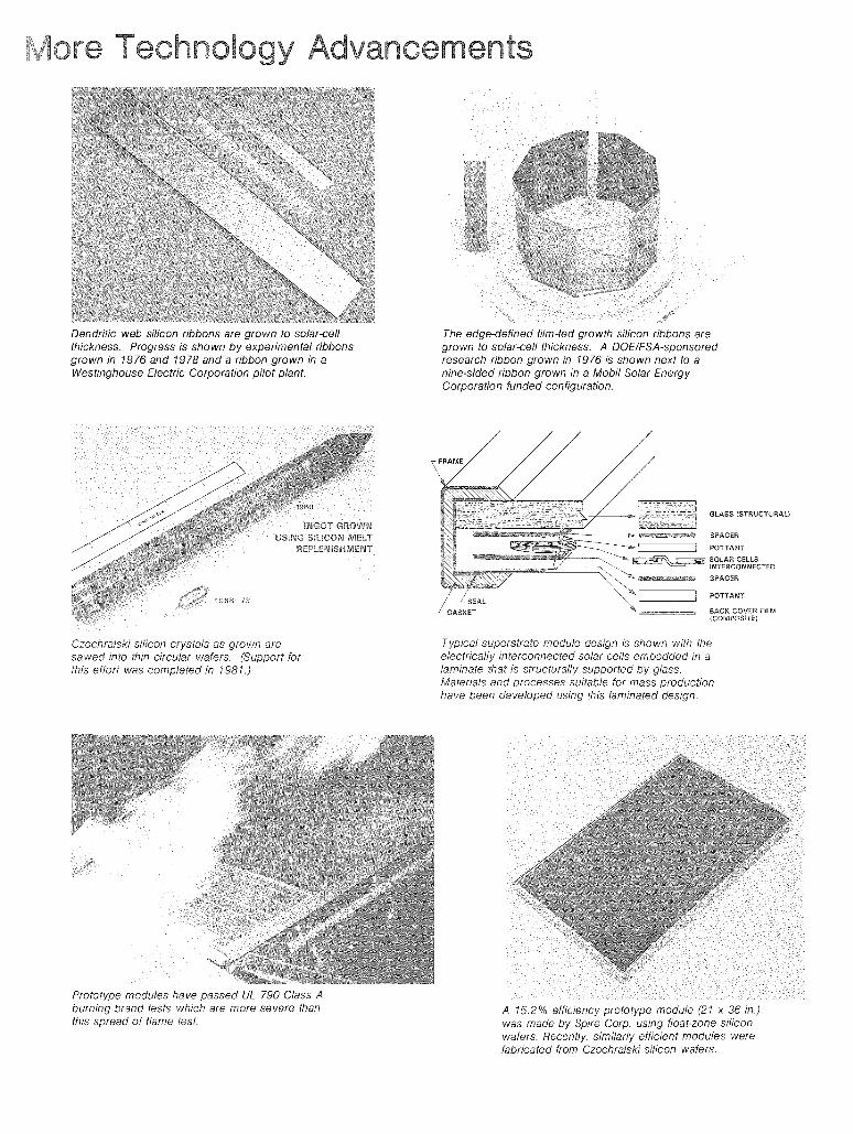
Dendritic web silicon ribbons are grown to solar-eellthickness. Progress is shown by experimental ribbonsgrown in 1976 and 1978 and a ribbon grown in aWestinghouse Electric Corporation pilot plant.
The edge-<iefined film-fed growth silicon ribbons aregrown to solar-eell thickness. A DOE/FSA-sponsoredresearch ribbon grown in 1976 is shown next to anine-sided ribbon grown in a Mobil Solar EnergyCorporation funded configuration.
FRAME
GLASS (STRUCTURALI
SPACER
I I POTTANT
[~~~~ fN~lE~~g~~lESCTED
SPACER
POTTANT
BACK COVER FilM{COMPOSITE}
Czochralski silicon crystals as grown aresawed into thin circular wafers. (Support forthis effort was completed in 1981.)
Prototype modules have passed UL 790 Class Aburning brand tests which are more severe thanthis spread of flame test.
Typical superstrate module design is shown with theelectrically interconnected solar cells embedded in alaminate that is structurally supported by glass.Materials and processes suitable for mass productionhave been developed using this laminated design.
A 15.2% efficiency prototype module (21 x 36 in.)was made by Spire Corp. using float-zone siliconwafers. Recently, similarly efficient modules werefabricated from Czochralski silicon wafers.
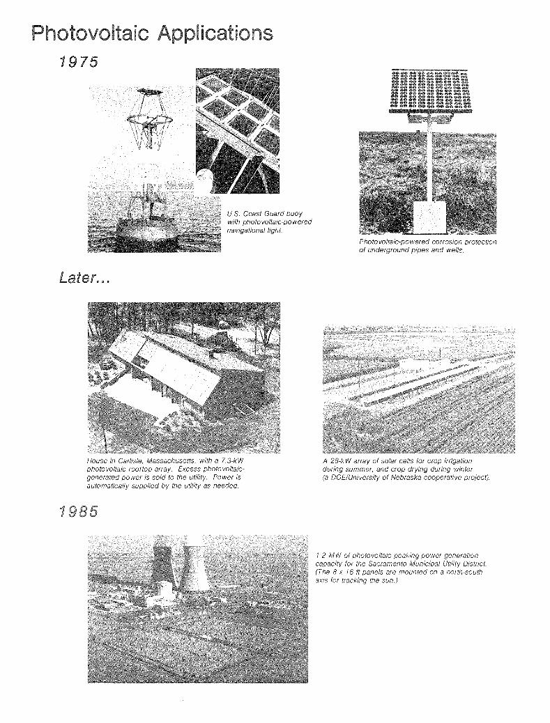
otovoltaic Applications1975
u.s. Coast Guard buoywith photovoltaic-powerednavigational light.
Later...
House in Carlisle, Massachusetts, with a 7.3-kWphoto voltaic rooftop array. Excess photo voltaicgenerated power is sold to the utility. Power isautomatically supplied by the utility as needed.
Photo voltaic-powered corrosion protectionof underground pipes and wells.
A 28-kW array of solar cells for crop irrigationduring summer, and crop drying during winter(a DOE/University of Nebraska cooperative project).
1
1.2 MW of photo voltaic peaking-power generationcapacity for the Sacramento Municipal Utility District.(The 8 x 16 It panels are mounted on a north-southaxis for tracking the sun.)