electrically small dipole antenna probe for quasi-static ... · ii preface with acknowledgements i...
TRANSCRIPT

Electrically Small Dipole Antenna Probe
for Quasi-static Electric Field Measurements
by
Adnan Zolj
B.S. Electrical Science and Engineering
Massachusetts Institute of Technology, 2010
SUBMITTED TO THE DEPARTMENT OF ELECTRICAL AND COMPUTER ENGINEERING
IN PARTIAL FULFILLMENT OF THE REQUIREMENTS FOR THE DEGREE OF
MASTER OF SCIENCE
IN ELECTRICAL AND COMPUTER ENGINEERING AT THE
WORCESTER POLYTECHNIC INSTITUTE
MARCH 2018
© 2018 Adnan Zolj. All rights reserved.
The author hereby grants WPI permission to reproduce
And to distribute publicly paper and electronic
Copies of this thesis document in whole or in part
In any medium now known or hereafter created.
Signature of Author: ____________________________________________________________________
Department of Electrical and Computer Engineering
March 23, 2018
Approved By: _________________________________________________________________________
Dr. Sergey Makarov
Thesis Supervisor
Approved By: _________________________________________________________________________
Dr. Aapo Nummenmaa
Thesis Committee Member
Approved By: _________________________________________________________________________
Dr. Greg Noetscher
Thesis Committee Member
Approved By: _________________________________________________________________________
Dr. Reinhold Ludwig
Thesis Committee Member
Accepted By: _________________________________________________________________________
Dr. John A. McNeill
Department Head

i
Electrically Small Dipole Antenna Probe
for Quasi-static Electric Field Measurements
by
Adnan Zolj
Submitted to the Department of Electrical and Computer Engineering
on March 23, 2018 in Partial Fulfillment of the
Requirements for the Degree of Master of Science in
Electrical and Computer Engineering
ABSTRACT
The thesis designs, constructs, and tests an electrically small dipole antenna probe for the measurement of
electric field distributions induced by a transcranial magnetic stimulation (TMS) coil. Its unique features
include high spatial resolution, large frequency band from 100 Hz to 300 kHz, efficient feedline isolation
via a printed Dyson balun, and accurate mitigation of noise. Prior work in this area is thoroughly reviewed.
The proposed probe design is realized in hardware; implementation details and design tradeoffs are
described. Test data is presented for the measurement of a CW capacitor electric field, demonstrating the
probe’s ability to properly measure conservative electric fields caused by a charge distribution. Test data is
also presented for the measurement of a CW solenoidal electric field, demonstrating the probe’s ability to
measure non-conservative solenoidal electric fields caused by Faraday’s law of induction. Those are the
primary fields for the transcranial magnetic stimulation. Advantages and disadvantages of this probing
system versus those of prior works are discussed. Further refinement steps necessary for the development
of this probe as a valuable TMS instrument are discussed.
Thesis Supervisor: Sergey Makarov
Title: Professor of Electrical and Computer Engineering

ii
Preface with Acknowledgements
I would like to thank Vicor Corporation for their generous financial support of my master’s studies for
which this thesis is but a part. I would like to thank Dr. Sergey Makarov, Dr. Aapo Nummenmaa and Dr.
Lucia Navarro de Lara for their mentorship on this thesis. I would like to thank Mr. Franco Baudino for
his assistance in the initial prototyping and initial discussions of this thesis.

iii
TABLE OF CONTENTS
List of Figures ................................................................................................................................................ v
List of Tables ............................................................................................................................................... vii
1 Introduction .......................................................................................................................................... 1
1.1 Prior Work on Electric Field Probes for TMS Characterization ..................................................... 1
1.1.1 Bioelectrode-based Electric Field Probes.............................................................................. 2
1.1.2 ∂B⁄∂t probes using a small loop ............................................................................................ 4
1.1.3 ∂B⁄∂t probes using a long rectangular loop .......................................................................... 4
1.1.4 ∂B⁄∂t probes using a triangular loop .................................................................................... 4
1.2 Other Prior Work on Probes for EM Field Measurements ........................................................... 5
1.2.1 Small Dipole with Capacitive Load ........................................................................................ 5
1.2.2 Small Dipole with Diode/Thermocouple Loads..................................................................... 6
1.2.3 Electro-optic Probes .............................................................................................................. 6
1.3 Contribution of this Work ............................................................................................................. 7
2 Electrical Design and Implementation .................................................................................................. 9
2.1 Dipole and Balun Hardware .......................................................................................................... 9
2.2 Instrumentation Hardware ......................................................................................................... 11
2.3 Design Process and Tradeoffs ..................................................................................................... 12
2.4 Final Design Parameters ............................................................................................................. 14
3 Experimental Procedures and Setup................................................................................................... 16
3.1 Frequency Response ................................................................................................................... 16
3.1.1 Differential-mode Gain ....................................................................................................... 16
3.1.2 Common-mode Gain ........................................................................................................... 16
3.2 Transient Response ..................................................................................................................... 16
3.3 Quasistatic Electric Field of Parallel Plate Capacitor ................................................................... 17
3.4 Quasistatic Electric Field of Solenoid .......................................................................................... 17
4 Experimental Results and Discussion .................................................................................................. 19
4.1 Frequency Response ................................................................................................................... 19
4.1.1 Differential-mode Gain ....................................................................................................... 19
4.1.2 Common-mode Gain ........................................................................................................... 20
4.2 Transient Response ..................................................................................................................... 20
4.3 Quasistatic Electric Field of Parallel Plate Capacitor ................................................................... 21

iv
4.4 Quasistatic Electric Field of Solenoid .......................................................................................... 23
5 Conclusion and Future Work .............................................................................................................. 27
6 Bibliography ........................................................................................................................................ 29
7 Appendix A: Ancillary Circuitry on Instrumentation PCB .................................................................... 33
8 Appendix B: Soft-switched MOSFET-based Stimulator ....................................................................... 36

v
LIST OF FIGURES
Figure 1: The following is a caricature of the loaded probe concept as proposed by Swiontek [8]. The
bioelectrode surfaces normal to the current density being measured are processed to have a very low
charge transfer resistance, RCT. As such current readily enters the loaded probe forming a current divider
with the medium. The load resistor is chosen to match the current density at the low RCT surfaces of the
probe with that of the medium. ................................................................................................................... 3
Figure 2: a) – Zoom-in of the 5mm printed dipole; b) – the dipole, balun and instrumentation assembled
together; c) – a simplified schematic for the complete electric field probe; biasing and other ancillary
circuitry are omitted. .................................................................................................................................... 9
Figure 3: Stackup for PCB of dipole and balun. Copper layers are 1 oz. thick (1.35mils). Prepreg thickness
between layers 1-2 and layers 3-4 is around 9.5mils. Thickness of center core material between layers 2-
3 is about 39mils. ........................................................................................................................................ 10
Figure 4: Top view of PCB for dipole and balun. Dipole and feedlines are shown on layer 2. Layers 1,3, 4
are the shield of the balun. The layers are stitched together with the vias denoted as green dots. ......... 10
Figure 5: Photograph showing the rework needed to eliminate the loop made by the SMA connector
assembly required by the partitioning of the design into two PCBs. The feedlines are cut on the top layer
before they reach the pads for the SMA center conductors on both the dipole/balun PCB and the
instrumentation PCB. The feedlines are routed through air using a differential pair made using AWG32
insulated wire. ............................................................................................................................................ 11
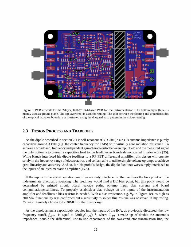
Figure 6: PCB artwork for the 2-layer, 0.062” FR4-based PCB for the instrumentation. The bottom layer
(blue) is mainly used as ground plane. The top layer (red) is used for routing. The split between the
floating and grounded sides of the optical isolation boundary is illustrated using the diagonal strip
pattern in the silk-screening. ...................................................................................................................... 12
Figure 7. a) – Simplified INA half-circuit noise model; b) – computed signal-to-noise ratio following Eq.
(1); note that in is set to 0 for these calculations. ....................................................................................... 13
Figure 8: This is a repeat of Figure 2c) to improve the readability of this section ..................................... 15
Figure 9: Parallel plate capacitor setup for parallel capacitor experiments. .............................................. 17
Figure 10: Shield is placed between length of coil and dipole oriented along the circulating magnetic
vector potential of the coil.......................................................................................................................... 18
Figure 11: The differential mode conversion factor is normalized to the data point at 3kHz. The
conversion factor at 3kHz is 0.227V on the output for 1V/cm of input electric field strength. ................. 19
Figure 12.. The common-mode gain is due to the parasitic capacitance bridging the isolation barrier of
the HCNR201. .............................................................................................................................................. 20
Figure 13. Transient response of the probe. CH1 (blue) is voltage of the driven plate of the parallel plate
capacitor. CH2 (red) is the output voltage of the electric field probe. a) –AC-coupled probe output
response to a 100 Hz square wave; b) – response to a 10 kHz square wave; c) – response to a 100 kHz
square wave with an artifact; d) –the same result as in c) but after shorting the isolation barrier. .......... 21
Figure 14. Vector field plot of electric field. Only x-hat components of the E-field were measured in the
region from x=0 to x=4 and y=-4 to y=4 ...................................................................................................... 22
Figure 15: Streamlines of the E-field vector field shown in Figure 14. ....................................................... 22
Figure 16. Dominant electric-field component inside and outside the parallel-plate capacitor setup
described in section 4.3. The dotted lines represent the capacitor plates. The capacitors were driven by a
vi
differential voltage amplitude of 7.6V, corresponding to an expected field strength of 1.84V/cm
between the plates. .................................................................................................................................... 23
Figure 17: The coil setup of section 3.4 was altered to align the dipole wings along the length of the coil
where there is naturally no -∂A⁄∂t. The left waveform in Figure 17 measures the probe output voltage
when there is no shield between the dipole and the coil. The right waveform measures the probe output
voltage when the shield is inserted. ........................................................................................................... 24
Figure 18: Initial data reduction comparing measured data to expected data for the solenoidal field tests
.................................................................................................................................................................... 24
Figure 19: Illustration showing parasitic dB/dt loop made by SMA connector bridge. .............................. 25
Figure 20: Expected Probe output when only the contribution from the dB/dt loop is include. ............... 25
Figure 21. The measured dA/dt versus the expected dA/dt as evaluated by the expression in [39] ........ 26
Figure 22: Measured induced electric field waveform at x=4.524cm; the SNR at these measurement
amplitudes was improved by averaging the waveform 64 times resulting in the waveform shown. CH1
(blue) is the coil current measured with a separate current probe in series with the coil, and CH2 (red) is
the output voltage of the electric-field probe. The excitation frequency is 3.846kHz. .............................. 26
Figure 23. Block diagram showing battery power and push-button state machine .................................. 33
Figure 24. Placement of blocks shown in Fig. 23. ....................................................................................... 34
Figure 25. Simple FSM for high-pass filter (HPF) bypass and ON/RESET control........................................ 34
Figure 26. This plot shows the measured differential mode gain response with the high-pass filter
enabled. The high-pass filter was implemented as a 4th order Bessel filter with corner frequency at
360Hz, providing 50dB of attenuation at 60Hz. The data was normalized to the conversion gain at 3kHz,
which measured to be 0.227V of output voltage for 1V/cm of incident electric field. The inclusion of this
filter was intended as a test-mode. ............................................................................................................ 35
Figure 27. Schematic for a bi-stable current pulse generator for induced E-field measurements with a
solenoid. Decoupling/bypass capacitors and unused circuits (in multi-circuit parts) are not shown. ....... 36
vii
LIST OF TABLES
Table 1: Key Performance Metrics for E-field Probe .................................................................................. 15
Table 2: Impedance of Solenoid for Induced Electric Field Measurements ............................................... 18
1
1 INTRODUCTION
Transcranial magnetic stimulation (TMS) is a commonly used tool in the academic study of the brain and
for the clinical treatment of certain neuropsychiatric conditions [1]. In TMS a coil is positioned above a
patient’s head and driven with a sequence of current pulses, inducing a sequence of electric field pulses in
a targeted region of the patient’s brain, which subsequently modulate the neural activity there [2].
Given the targeted nature of its application a TMS coil’s design is naturally predicated not only on the
geometry of the coil but also on the geometry of the brain under stimulation, e.g. it size, its shape, and its
underlying tissue layer composition [3]. As such computational simulation methods often play a significant
role in the design of TMS coils. In fact, for the highest accuracy, simulation methods such as the boundary
element method (BEM) as demonstrated by Nummenmaa [3] may be the best tool available for researchers
and clinicians who need to accurately pinpoint the exact area of stimulation given a particular coil and target
specimen.
Our computational capability will only improve with time. We should be wary, however, of believing
too much in our models lest they lead us astray; as the old adage goes it is always good to trust but always
better to verify. And in this spirit, the aim of this work is to add to the body of knowledge concerned with
the physical measurement of coil performance. In what follows we demonstrate a way to measure the
induced electric field distribution of a coil in air using an electrically small dipole antenna. This method
has some advantages and some disadvantages compared with the methods and probes of prior work, whose
operation we will briefly review before delving into the details of our approach.
1.1 PRIOR WORK ON ELECTRIC FIELD PROBES FOR TMS CHARACTERIZATION
As Makarov [4] explains the brain can be modeled as a weakly conducting medium satisfying the thin
limit condition, i.e. the skin depth is much greater than the greatest dimension of interest of the object, and
the general magneto-static approximation, whereby displacement current are neglected, for frequencies of
interest for the object.
In neglecting displacement currents the relationship between current density, 𝐽, and the magnetic field,
, becomes:
∇ × = 𝐽 (1)
whereas the electric field:
= −𝜕𝐴
𝜕𝑡− ∇𝜑 (2)
must continue to be expressed in terms of both the magnetic vector potential, 𝐴, and the electric scalar
potential, φ. Lastly, the eddy current, 𝐽𝑠, is related to the electric field and bulk conductivity, 𝜎, by:
𝐽𝑠 = 𝜎 (3)
The consequence of the thin limit condition with respect to TMS is that since the magnetic field due to
the coil dominates any secondary fields created by eddy current, the electric field contribution due to
−𝜕𝐴 𝜕𝑡⁄ in (2) is determined using coil current alone [4]. The contribution due to −∇𝜑 comes from charge
accumulation at conductivity boundaries in tissue due to the eddy current flow [4].

2
Both contributions to the electric field as expressed in (3) are important for neuromodulation [5].
Therefore, in the review of prior work in the subsections that follow a distinction will be made between
probes that can only capture the primary contribution to the electric field, or −𝜕𝐴 𝜕𝑡⁄ , and probes that can
capture the complete electric field as describe in (2) and under what assumptions they do so.
The major types of probes that have been used to measure the electric fields patterns of TMS coils in the
past are the following:
a) electric field probes using bioelectrodes;
b) 𝜕 𝜕𝑡⁄ probes using a small loop;
c) 𝜕 𝜕𝑡⁄ probes using a long rectangular loop;
d) 𝜕 𝜕𝑡⁄ probes using a triangular loop.
Among these only a) is designed to be used in tissue or saline solution-based phantoms, and only a) can
measure the complete electric field of (1) under general conditions. The rest of the probes are meant to be
used in air. The probes in b) and c) can only measure the primary electric field. The triangular 𝜕 𝜕𝑡⁄ probe
of d) can be used to make a phantom measurement of the complete electric field found in a spherically
symmetric volume conductor.
1.1.1 Bioelectrode-based Electric Field Probes
A bioelectrode is simply an electrode designed to be compatible for measurements in bodily tissues [6].
The free charge carriers in the metal conductor that makes up the electrode are electrons. The free charge
carriers in bodily tissue are ions available in solution. The simplest model for a bioelectrode in an
electrolytic solution is a built-in electric potential (a voltage source) in series with a parallel resistor and
capacitor [6]. This voltage source is sometimes called the half-cell potential or the reversible potential [6].
The resistance is called the charge transfer resistance, or RCT, and represents the change in the voltage drop
across the electrode-electrolyte interface with current flow [6]. The capacitance is called the double-layer
capacitance, or CDL, and is reviewed in great detail by Bockris in [7].
Broadly speaking, there are two ways to apply bioelectrodes in measuring induced electric field during
TMS. One method, called the loaded probe method [8], assembles two bioelectrodes to create an ammeter
loosely speaking. The other method interfaces the bioelectrodes to a high impedance amplifier to create a
voltmeter.
The most significant works using the loaded probe method in the evaluation of electric fields induced by
TMS are those of Tay [9], [10], where TMS measurements were made in saline solution and in the brain of
anesthetized cats. Although it is not precisely clear how Tay constructed her loaded probes based on her
works alone, earlier works by Swiontek [8] and Deutsch [11] shed some light on nature of the construction.
An illustration of Swiontek’s loaded probe is shown in Fig. 1. In essence Swiontek proposes a probe
whereby two opposite-facing sides of a small rectangular insulating volume are plated with a low RCT
bioelectrode surface that readily passes current to an external load resistance, which is matched to the
electrolytic solution under test so that the probe in a way electrically transparent to the medium [8]. In other
words, if the spacer thickness in Fig. 1 is d and the surface area of the low RCT electrodes is A, then ideally
the load resistance would be RL=Ed/(JA), where E and J are the electric field and current density normal to
the low RCT surfaces respectively. An interesting feature of the loaded probe is that the electrode surface
area can be traded off for signal-to-noise ratio (SNR); i.e. assuming d is fixed, A can be increased and
thereby RL can be decreased reducing its thermal noise. One disadvantage is that the low RCT surface shorts
out the lateral electric field. Another disadvantage is that a large volume of the medium is potentially
displaced by this electrode and that in a time-vary magnetic field the spacing between the electrode surfaces

3
might be problematic owing to the non-conservative nature of the magnetic field [12].
Figure 1: The following is a caricature of the loaded probe concept as proposed by Swiontek [8]. The bioelectrode
surfaces normal to the current density being measured are processed to have a very low charge transfer resistance,
RCT. As such current readily enters the loaded probe forming a current divider with the medium. The load resistor is
chosen to match the current density at the low RCT surfaces of the probe with that of the medium.
The other popular method of constructing a bioelectrode-based probe is as a voltmeter so to speak. It is
described so as the driving point impedance looking into the probe tips is designed to be high as the
bioelectrode feedlines are ultimately interfaced to a high impedance voltage amplifier. Early references for
this method can be found in the works of Durand [13], Tofts [14], Hart [15] and Maccabee [16]. In this
method the bioelectrodes are formed in the shape of an electric dipole that maintains very close spacing
between the feedlines [12].
One important requirement not explicitly stated in prior works on the short dipole probe is that the passive
interface impedance of the bioelectrodes, e.g. RCT in parallel with CDL, should ideally be much lower than
the input impedance of the downstream differential amplifier. This is because the passive interface
impedance is not stable; both RCT and CDL can change with time, temperature, frequency and electrolyte
concentration [17].
A second important requirement for the short dipole probe is that the feedlines must be routed together
as closely as possible. The voltage seen by the downstream differential amplifier is the superposition of the
voltage drop along the bioelectrodes due to (2) and the contributions of −𝜕𝐴 𝜕𝑡⁄ along the feedlines. Since
the magnetic field is non-conservative, exact cancellation of the feedline contributions can only occur if the
feedlines are coincident in space as explained and demonstrated experimentally by Glover [12].
The greatest disadvantage with the bioelectrode-based approach, whether a loaded probe or short dipole
probe is considered, compared with other approaches is that the experimental setup is the most complicated,
primarily owning to the fact that it is a wet science. In principle, however, if a suitably detailed phantom
can be built or in vitro measurements can be performed then accurate measurement of the complete electric
field are possible, which is a claim no other probe of the prior art can make.

4
1.1.2 ∂B⁄∂t probes using a small loop
A small loop can be used to measure the magnetic field or flux. If the x, y and z components of the
magnetic field over space are sampled properly, the inverse problem for the vector potential ∇ × 𝐴 =
could be solved. These probes can only measure the solenoidal electric field −𝜕𝐴 𝜕𝑡⁄ . The advantage of
small loop probes is that they are very easy to construct and that the measurements can be made in air. The
disadvantage is that only the solenoidal electric field can be derived, and that three very small orthogonal
loops and very many measurements are required to accurately restore the electric field.
1.1.3 ∂B⁄∂t probes using a long rectangular loop
Epstein [18] pioneered a clever rectangular loop probe to measure the solenoidal electric field without
solving the inverse problem. His approach was successfully applied most recently by Salinas [19], [20],
where he refers to the rectangular loop as a 3D eddy current probe. The basic construction of this 𝜕 𝜕𝑡⁄
probe consists of a long rectangular loop, whose long sides are determined by the amount of distance
required for the magnetic vector potential to fall off to negligible levels [18]. The short sides are determined
by the desired spatial resolution [18]. One short side is placed at the location and in the direction for the
desired primary electric field measurement, while the other short side is connected to some voltage
measuring devices like an oscilloscope [18]. If the long sides are centered along an axis of symmetry with
respect to the magnetic vector potential, then the −𝜕𝐴 𝜕𝑡⁄ contributions along the long sides cancel out
and the total emf is simply the length of the short side multiplied by its −𝜕𝐴 𝜕𝑡⁄ ; this is the voltage that is
ultimately measured [18].
Tofts [14] criticized this approach for only being able to measure the solenoidal electric field along an
axis of symmetry. However, that assessment is only true if a single measurement is permitted. Salinas [19]
claims the design can be applied off of the axis of symmetry by using two measurements; however, it is not
clear to me that his two-measurement technique is generally applicable. Unfortunately, Salinas was never
contacted for clarification on his claim. The advantage of the rectangular loop is that measurements can be
made in air and that it is relatively easy to construct. Salinas [20] suggested a simple way to create a two-
axis probe using two orthogonal rectangular loops on a single support rod.
The advantage of the rectangular loop is that measurements can be made in air and that it is relatively
easy to construct. The disadvantages of the probe are that it can only measure the primary electric field and
it may only be able to do so along a line of symmetry where the −𝜕𝐴 𝜕𝑡⁄ along the long sides cancels [18],
[14]. I am not convinced of Salinas’ claim [19] that with two measurements the unbalanced −𝜕𝐴 𝜕𝑡⁄
contributions on the long sides can be compensated for, but let it be known that such a claim is out there.
1.1.4 ∂B⁄∂t probes using a triangular loop
The triangular loop-based 𝜕 𝜕𝑡⁄ probe was created by Niemenin [21]. His probe, which he called the
TMS calibrator, was inspired by prior work done by Ilmoniemi [22], [23] on the inverse and forward
problems of magnetoencephalography (MEG).
The basis for the operation of the Niemenin’s TMS calibrator is a subtle argument that hinges on the fact
that an externally applied magnetic field cannot induce a radial current in a spherical conductor [24]. Using
this fact, a proof can be constructed to show that the external magnetic field generated outside of a

5
spherically symmetric volume conductor by an internal tangential current dipole and its associated volume
currents is indistinguishable from that of a triangular current loop in free space that includes the original
primary current dipole and whose vertex is the center of the original volume conductor [21]. Once this is
proved it can be argued by reciprocity that the emf measured by the triangular loop so constructed is the
same as the complete electric field integrated along the aforementioned tangential length in a spherically
symmetric volume conductor [21]. An elegant graphical proof of this can be found in Niemenin’s paper
[21].
The advantages of Niemenin’s triangular loop probe are that it is easy to construct and its measured emf
is a phantom for the complete electric field at point inside a spherically symmetric volume conductor.
Furthermore, Niemenin’s triangular loop-based probe can be used in air. Its main disadvantages are that it
cannot be used as a phantom for general volume conductor shapes or arbitrary conductivity profiles. One
final disadvantage, albeit minor, is that a given triangular probe can only be used to sweep the electric field
at a fixed radial distance. If a different sweep radius is desired the probe’s vertex cannot simply be shifted
in space, instead a new triangular probe with shorter radial side lengths must be constructed [21].
1.2 OTHER PRIOR WORK ON PROBES FOR EM FIELD MEASUREMENTS
1.2.1 Small Dipole with Capacitive Load
In a review of standard probes for electromagnetic field measurements, Kanda [25] discusses the idea of
an electrically short dipole loaded with a capacitive load. Due to its capacitive self-impedance, the
electrically short dipole antenna will yield a frequency independent transfer characteristic when driving a
capacitive load. Kanda [25] experimentally demonstrates this feature using a 15-cm dipole (6-mm radius)
connected to a 13 pF FET amplifier to achieve a flat frequency response from 2kHz to 400MHz.
The low frequency cutoff of this E-field probe is determined by the RC time constant made between the
input resistance of the FET amplifier working against the combined input capacitance of the FET amplifier
together with the antenna capacitance of the dipole. The high frequency cutoff is fundamentally limited by
the half-wave resonant frequency of the dipole. The dipole must be operated below its half-wave resonant
frequency in order to be considered electrically small so that its impedance remains predominantly
capacitive. One easy way to extend the high frequency cut off is to use a physically smaller dipole. The
tradeoff here is between bandwidth and signal-to-noise ratio as explained by Smith [26]. Another limitation
at the time that Kanda wrote his paper [25] was the unavailability of differential FET amplifiers with
adequate high frequency common-mode rejection. To extend the frequency range further the FET
amplifiers would have to be replaced with a diode detector as describe in section 1.2.2, but this is a whole
different animal as it is no longer able to measure the time-domain evolution of the E-field [25]. The beauty
of the original approach is the time-domain behavior can accurately be measured as long as the spectra is
contained within the bandwidth of the E-field probe.
The end application of Kanda’s capacitively loaded small dipole antenna was in the measurement of EMI
and EMC problems and determination of safe levels for electromagnetic radiation [25]. In recent years,
other researchers have continued to use electrically small dipoles to create E-field probes for EMC and EMI
test purposes [27], [28]. The most exciting new research I have found in this sphere is by Schmid & Partner
Engineering AG (SPEAG) in Zurich, Switzerland, whereby they combined the electrically small,
capacitively loaded dipole with an optical power and data link resulting in a fully robotized system that is
able to sweep out the field in the vicinity of a device-under-test (DUT) for EMC/EMI characterization [29].

6
1.2.2 Small Dipole with Diode/Thermocouple Loads
To extend the high frequency range of the E-field probes discussed in section 1.2.1 the FET amplifier of
the last section can be replaced with a diode or thermocouple detector. This system is a whole different
animal from the E-field probes discussed in the last section. For starters the probe is no longer able to
accurately measure pulse waveforms in the time domain. It either outputs a signal proportional to the square
of the electric field magnitude or the peak depending on the signal level [25], [30]. As such the probe is
designed to be used as a DC instrument, whose output is ultimately connected through a DC voltmeter.
In the case of the diode load the reason for this behavior is owed to the non-linear I-V characteristic of
the diode and its relative slow response time relative to the RF signal from the antenna. As a result of these
two characteristics, when given a continuous wave (CW) signal the diode will be driven into its reverse-
bias region as the junction capacitance is much lower when the diode is reversed-biased, meaning the
negative going pulse will have a much easier time driving the diode’s junction capacitance than that of
positive going pulse. If the amplitude of the input signal is large the diode will be driven deeper into reverse
bias where its junction capacitance becomes more linear. This is the region where the probe output is
proportional to peak signal level. With low input signal levels, the diode is biased close to it zero bias point.
Owing to this fact the probe’s output now has a square-law dependence on the input field [25]. Details on
the operation of the small dipole with a thermocouple detector is explained by Bassen [30].
The last detail I would like to mention about this class of E-field probes is that since they are designed to
only measure the magnitude or the square magnitude of the electric field the dipole is interfaced to the
downstream instrumentation via a very resistive transmission line to filter out the RF signal content and to
minimize the extent to which the probe scatters the incident field as explained by Bassen [30]. In particular,
Bassen [30] explains the high resistance transmission line can be formed using carbon impregnated Teflon
strips with resistivity of 4 megaohm/meter.
1.2.3 Electro-optic Probes
Electro-optic (EO) probes use the fact that an applied electric field changes some optical properties of an
EO material in order to indirectly infer the electric field by measuring the change in the relevant optical
properties [31]. Jarrige [31] developed an EO probe suitable for bioelectromagnetic investigation over a
frequency range from 1KHz to 10GHz. His probe is able to extract the vectoral electric field and was an
extension of prior work completed by Wakana [32] and Bernier [33]. The use case for these probes seems
to be in the measurement of specific absorption rates (SAR) of electromagnetic radiation; in fact, Jarrige
[31] claims that his EO crystal has a relatively permittivity of 42, which he implies makes it a good
candidate for testing of biological media, which has a similar relative permittivity at a frequency of interest,
meaning that the crystal should be transparent to the environment in which it is submersed. Zhu [34] claims
that the one drawback to electro-optic technology is that the EO materials can have piezoelectric properties,
which limit low frequency operation to tens of kilohertz.
Given the discussion in the previous paragraph it seems that EO probes are likely competitors to the small
dipoles loaded with diode detectors described in section 1.2.2. One obvious drawback I see to the EO probes
described in the works of Jarrige [31], Wakana [32] and Bernier [33] is the high computational and
optoelectronic overhead required for its operation.

7
1.3 CONTRIBUTION OF THIS WORK
From section 1.1 we see that there was and still is interest in being able to evaluate electric field
measurements of TMS coils in air. This is probably partially due to the fact that air is a more controlled
medium than saline solution, which makes air the better candidate for making meaningful comparisons
between measurements and simulations (i.e. there may be less guesswork involved with air as the medium.)
Furthermore, owing to the relative simplicity of air as a test medium compared to saline solution, the
automation of in-air electric field measurements should in principle be more easily accomplished. In fact,
Niemenin [21] constructed a fully robotized measurement system utilizing his triangular loop that was able
to sweep out the electric field pattern on a hemispherical surface with the push of a button.
The trouble with loop-based approaches is that they in general cannot measure the complete electric field,
including the contributions from both the electric scalar potential due to surface charges and the magnetic
vector potential due to the coil current. This is simply due to the fact that the −∇𝜑 contribution comes from
surface charge accumulation normal to the eddy current density in a medium of varying conductivity; in
other words, without the actual volume conductor (e.g. saline solution) there are no eddy currents and hence
no induced surface charges and hence zero −∇𝜑. Niemenin’s approach [21] using the triangular loop
represents the best method known to date for measuring the electric field of a TMS coil in air. Its only
drawback is that the conditions under which the emf picked up by his triangular loop is proportional to the
field around a tangential current dipole (including both the primary and secondary field components) are
that the volume conductor be perfectly spherically symmetric; note that this spherical symmetry does allow
conductivity to vary radially [21]. These conditions limit the general-purpose applicability of Niemenin’s
probe because the brain, even if limited to cranial cavity is not perfectly spherical and the conductivity
profile is not always perfectly radial [3]. With small deviations in the spherical symmetry of the volume
conductor the prevailing belief that the TMS coil cannot induce radial currents is no longer true as explained
in detail by Mosher in his Review on the Importance of Volume Currents [35]. All of this said in no way
should diminish the great utility of Niemenien’s probe as a calibration instrument; with it numerical
simulation of coils and spherical conductor models can be validated against accurate, in air measurements,
which is truly remarkable [21].
To measure the complete electric field the bioelectrode-based approach of section 1.1.1 is the only way
known to date. The loaded probe approach is of limited applicability in my opinion due to the non-
conservative nature of the magnetic field and to the fact that lateral electric fields can be shorted out by the
low RCT surface electrodes as was discussed in section 1.1.1. The best approach is the short dipole probe
owing to its high impedance, which should minimally distort the field distribution in the medium, and the
close spacing of the feedlines, which should minimize −𝜕𝐴 𝜕𝑡⁄ along the feedlines as explained by Glover
[12]. The largest drawback with the bioelectrode-based approach is the saline solution or tissue medium,
which would seem to require a lot of experimental due diligence to make sure experimentation is controlled.
In this thesis I propose to add a new probe for the measurement of electric fields of TMS coils. This probe
is simply the electrically short dipole antenna loaded with a capacitive load that was presented in section
1.2.1 but adapted for the evaluation of TMS coil performance. Its unique features include high spatial
resolution, large frequency band from 100 Hz to 300 kHz, efficient feedline isolation via a printed Dyson
balun, and good signal-to-noise properties. In this thesis I demonstrate how the probe can be used to
measure induced electric field pattern (due to −𝜕𝐴 𝜕𝑡⁄ ) of a coil in air. I also demonstrate how the probe
can be used to measure the electric field pattern (due to −∇𝜑) of a parallel-plate capacitor. Data for the
frequency and time-domain characterization of the probe is also presented.

8
In the context of the TMS probes of prior works the probe of this thesis is able to generally measure the
primary field component in air with a single measurement, which represents an improvement over the
rectangular loop. Furthermore, it should in principle be applicable in the measure of the complete electric
field inside saline solution phantom or tissue sample. This is not demonstrated in this work but is further
discussed in the conclusion.

9
2 ELECTRICAL DESIGN AND IMPLEMENTATION
In this section I will review in detail the design of the electrically small dipole probe of this thesis, which
will be referred to as the E-field probe from here on out. The E-field probe consists of a small dipole as
shown in Fig. 2a whose feedlines are capacitively coupled to the inputs of an optically isolated
instrumentation amplifier via a printed version of the Dyson balun [36], [37]. At face value the circuits
involved are not particularly challenging or difficult, which is great from an engineering perspective;
however, there are some subtleties related to the interplay between biasing, spatial resolution, frequency
range and signal-to-noise ratio, which I will discuss in the sections that follow.
I will first start by describing the implementation of the dipole and balun. Then I will present the
instrumentation, including hardware that goes beyond the core circuits shown in Figure 2c for the reader
interested in reproducing the probe of this work. With the hardware sufficiently described I will discuss the
design tradeoffs between spatial resolution, frequency range, biasing and the signal-to-noise ratio. In the
final section I will summarize the key performance metrics of the hardware implementation that was
ultimately realized.
Figure 2: a) – Zoom-in of the 5mm printed dipole; b) – the dipole, balun and instrumentation assembled together; c)
– a simplified schematic for the complete electric field probe; biasing and other ancillary circuitry are omitted.
2.1 DIPOLE AND BALUN HARDWARE
The dipole and balun were implemented using a standard 4-layer, 0.062” FR4-based PCB with stack-up
a) b)
c)

10
shown in Figure 3. To implement the printed, Dyson balun, which is equivalent to a shielded, balanced two-
conductor transmission line, only three layers are really necessary; the 4-layer structure was chosen as it is
inexpensive and easy to manufacture given the desired 0.062” total thickness. Although the resultant stack-
up is not symmetric with respect to the cross-section it is balanced with respect to the feedlines, which is
the key feature. The 0.062’’ thickness was driven by the desire to interface standard edge-mount SMA
connectors to the final assembly. Figure 4 shows the top view of the dipole and balun PCB. Layers 1,3 and
4 of the PCB were exclusively used as the shield and were stitched together with vias spaced 0.2” (or
0.508cm) apart on either side of the feedlines. The dipole and the feedlines were routed on inner layer 2
using 7mil (or 0.178mm) thick traces. The dipole length was 5mm and the gap between the feedlines was
8mils (or 0.203mm). The total feedline length was 6’’ (or 15.24cm).
Figure 3: Stackup for PCB of dipole and balun. Copper layers are 1 oz. thick (1.35mils). Prepreg thickness between
layers 1-2 and layers 3-4 is around 9.5mils. Thickness of center core material between layers 2-3 is about 39mils.
Figure 4: Top view of PCB for dipole and balun. Dipole and feedlines are shown on layer 2. Layers 1,3, 4 are the
shield of the balun. The layers are stitched together with the vias denoted as green dots.
The feedlines of this PCB are ultimately interfaced to a separate PCB where the instrumentation resides.
The separation of the dipole/balun from the instrumentation was so chosen to save on material costs in
anticipation of the iterative nature of electronics design; the idea was that it would be wasteful to do a re-
spin of the complete structure if only a small revision were required for one part. No good deed goes
unpunished, however, as the two PCBs required a SMA connector bridge as shown in Figure 2b, which was
a source of unwanted 𝜕 𝜕𝑡⁄ coupling during the solenoidal field testing, which is further discussed in
Section 4.4. In order to eliminate the parasitic 𝜕 𝜕𝑡⁄ coupling the feedline traces were ultimately cut on
either end of the SMA connector bridge as shown in Figure 5 and routed back along the same path they
came before jumping the gap by way of a differential pair made using AWG32 magnetic wire. In this case
the role of the SMA connector bridge was reduced to mechanical support and shield biasing.

11
Figure 5: Photograph showing the rework needed to eliminate the loop made by the SMA connector assembly required
by the partitioning of the design into two PCBs. The feedlines are cut on the top layer before they reach the pads for
the SMA center conductors on both the dipole/balun PCB and the instrumentation PCB. The feedlines are routed
through air using a differential pair made using AWG32 insulated wire.
2.2 INSTRUMENTATION HARDWARE
The instrumentation PCB was implemented using 2-layer, 0.062” FR4 stack-up with top and bottom layer
plated to 1oz. copper. The artwork for the design is shown in Figure 6. As the instrumentation is optically
isolated there are two separate ground planes for the floating circuits, which interface to the dipole/balun,
and the grounded circuits, which ultimately interface with an oscilloscope. The shield of the balun is
connected to the floating ground. The ground of the grounded circuits is connected to the outer conductor
of the output SMA connector, meaning that it will ultimately be connected to the oscilloscope ground. The
split between the two ground planes is denoted by the diagonally striped pattern in Figure 6.
The essential circuits comprising the instrumentation were already depicted Figure 2c), where it is also
noted that biasing and other ancillary circuits are omitted. The large volume of circuitry evident in Figure
6 is in large part due to the aforementioned biasing and ancillary circuits. As the operation of these
additional circuits is not particularly relevant to the operation of the E-field probe they will not be discussed
in depth in this section. The only significant thing to appreciate with respect to the additional circuits are
that they pertain to battery power operation, a simple push-button state-machine and an optional high-pass
filter for 60Hz suppression (intended as a debug mode.) For information on the ancillary circuitry refer to
Appendix A.
12
Figure 6: PCB artwork for the 2-layer, 0.062” FR4-based PCB for the instrumentation. The bottom layer (blue) is
mainly used as ground plane. The top layer (red) is used for routing. The split between the floating and grounded sides
of the optical isolation boundary is illustrated using the diagonal strip pattern in the silk-screening.
2.3 DESIGN PROCESS AND TRADEOFFS
As the dipole described in section 2.1 is self-resonant at 30 GHz (in air,) its antenna impedance is purely
capacitive around 3 kHz (e.g. the center frequency for TMS) with virtually zero radiation resistance. To
achieve a broadband, frequency independent gain characteristic between input field and the measured signal
the only option is to present a capacitive load to the feedlines as Kanda demonstrated in prior work [25].
While Kanda interfaced his dipole feedlines to a RF FET differential amplifier, this design will operate
solely in the frequency range of electrostatics, and so I am able to utilize simple voltage op-amps to achieve
great linearity and accuracy. And so, for this probe’s design, the dipole feedlines were simply interfaced to
the inputs of an instrumentation amplifier (INA).
If the inputs to the instrumentation amplifier are only interfaced to the feedlines the bias point will be
indeterminate practically speaking. The feedlines would find a DC bias point, but this point would be
determined by printed circuit board leakage paths, op-amp input bias currents and board
contamination/cleanliness. To properly establish a bias voltage on the inputs of the instrumentation
amplifier and feedlines a bias resistor is needed. With a bias resistance, e.g. 𝑅𝐵 in Figure 1c), as high as
500 MΩ functionality was confirmed but a sensitivity to solder flux residue was observed in my testing.
𝑅𝐵 was ultimately chosen to be 30MΩ for the final design.
As the dipole antenna capacitively couples into the inputs of the INA, as previously discussed, the low
frequency cutoff, 𝑓𝐿𝑂𝑊 , is equal to (2πRBCTOT)−1 , where 𝐶𝑇𝑂𝑇 is made up of double the antenna’s
impedance, double the differential line-to-line capacitance of the two-conductor transmission line, the

13
whole line-to-shield capacitance of the two-conductor transmission line, the common-mode input
capacitance of INA op-amp, the parasitic shunt capacitance of 𝑅𝐵 , and any additional external input
capacitance 𝐶𝐼𝑁. The additional input capacitance 𝐶𝐼𝑁 is a degree of freedom for lowering 𝑓𝐿𝑂𝑊. At the
same time, 𝐶𝐼𝑁 also attenuates the input signal resulting in a degradation of the SNR.
The SNR of the system is determined by the INA input stage alone. Downstream stages do not contribute
into the noise calculation due to the high gain of the INA, which should be set as large as possible given
bandwidth and accuracy requirements: in our implementation it was set to 20 V/V, which reduces the closed
loop bandwidth of our selected op-amp to 500 kHz. The noise contributors are the equivalent noise voltage
and equivalent noise current of the INA op-amps, 𝑒𝑛 and 𝑖𝑛, respectively, and the thermal noise from 𝑅𝐵
shown in Fig 7a. It is assumed that INA feedback resistors, 𝑅𝐺 and 𝑅𝐹, shown in Fig. 2 are chosen such
that their noise contributions are negligible.
Figure 7. a) – Simplified INA half-circuit noise model; b) – computed signal-to-noise ratio following Eq. (1); note
that in is set to 0 for these calculations.
The total input referred noise is approximately given by √(𝜋 2⁄ )𝑓𝐵𝑊𝑒𝑛2 + 𝑘𝐵𝑇 𝐶𝑇𝑂𝑇⁄ , where 𝑓𝐵𝑊 is the
bandwidth of the INA op-amp, 𝑘𝐵 is Boltzmann’s constant and 𝑇 is the absolute temperature in Kelvin.
Even with RB=30MΩ the noise contribution from 𝑖𝑛 turns out to be negligible compared with that of 𝑒𝑛 for
the OPA2325, which was the op-amp ultimately used and thus 𝑖𝑛 was omitted in the noise expression. The
input signal is determined by the full-scale input field 𝐸𝐹𝑆, the dipole length 𝑙𝐴, and the capacitive divider
made between the half-circuit antenna capacitance 𝐶𝐴 and 𝐶𝑇𝑂𝑇. The expression for the resultant SNR is
obtained in the form:
𝑆𝑁𝑅 = 20 log10 (𝐸𝐹𝑆𝑙𝐴𝐶𝐴
𝐶𝑇𝑂𝑇√(𝜋 2⁄ )𝑓𝐵𝑊𝑒𝑛2+𝑘𝐵𝑇 𝐶𝑇𝑂𝑇⁄
) (4)
A plot of Eq. 4 versus (𝐶𝑇𝑂𝑇 − 𝐶𝐴) is shown in Fig. 7b. The SNR of the system using the OPA2325 with
𝑒𝑛 = 10nV/√Hz is shown in blue and the SNR of a system using a noiseless amplifier is shown in red; the
difference between the curves is the noise figure of our circuit. In order to minimize this noise figure (i.e.

14
keep it less than 5dB) we should keep 𝐶𝑇𝑂𝑇 less than 100 pF. We also see that the SNR of our system falls
off at two different slopes. When 𝐶𝑇𝑂𝑇 is less than 20 pF but greater than 0.1pF the SNR degrades at a rate
of 10 dB/decade; whereas, when 𝐶𝑇𝑂𝑇 is greater than 20pF the SNR degradation slope becomes 20
dB/decade. This difference in slopes is due to the fact that the noise power saturates to a constant level
determined by 𝑒𝑛 alone when 𝐶𝑇𝑂𝑇 is greater than 20 pF, whereas the noise power decreases at a rate of 10
dB/decade when 𝐶𝑇𝑂𝑇 is less than 20 pF. The plateau seen at minimal (𝐶𝑇𝑂𝑇 − 𝐶𝐴) can be understood
analytically by taking the limit of Eq. (2) as 𝐶𝑇𝑂𝑇 → 𝐶𝐴. Since the self-capacitance of an electrically small
dipole is proportional to its length 𝑙𝐴 [25] we can replace 𝐶𝐴 in our expression with κ𝑙𝐴, where constant κ
has units of F/m and is the first coefficient of the power series expansion, and neglect the contribution from
𝑒𝑛 altogether, which yields
lim𝐶𝑇𝑂𝑇→𝐶𝐴
𝑆𝑁𝑅 = 20 log10 (𝐸𝐹𝑆
√𝑘𝑏𝑇√𝜅(𝑙𝐴)3/2) (5)
Eq. (5) illustrates a tradeoff between the spatial resolution and the maximum achievable SNR. For a given
dipole length, 𝑙𝐴, the only means to improve the SNR is to increase the full-scale electric field or to decrease
temperature. The derivation presented here is simplified; a more detailed derivation of a similar system can
be found in [26].
The design of the rest of the system is less critical and I will present it expeditiously. The instrumentation
amplifier gives us a differential output. A single-ended output and more gain is ultimately needed to
interface with the HCNR201. To accomplish this, a simple difference amplifier was used to do the
differential to single-ended conversion.
The last part of the design is galvanic isolation via the Broadcom HCNR201 matched opto-coupler shown
in Fig. 2c. The purpose of the galvanic isolation is to suppress any common-mode current. The optical
isolation amplifier of Fig. 2c depends on tight matching of photodiodes PD1 and PD2 and equal
illumination by the LED, which is guaranteed by the design of the HCNR201. The first op-amp drives the
PNP and ultimately the LED to make the current in PD1 and PD2 equal to V𝐼𝑁/𝑅𝑉𝐼 . Hence the output
voltage, V𝑂𝑈𝑇, will be equal to V𝐼𝑁 to within the bandwidth of the cascade of amplifiers, which is set by 𝐶1
and 𝐶2.
Both sets of circuits, on either side of the isolation barrier, are battery powered to eliminate any potential
common-mode noise issues.
2.4 FINAL DESIGN PARAMETERS
Figure 8 shows the simplified schematic for the complete electric field probe repeated from Figure 2 for
the reader’s convenience; biasing and other ancillary circuitry are omitted. The dipole-facing and output
facing circuits are galvanically isolated via U4 and separate batteries are used to supply the bias power. The
component values used for the final implementation are: RB= 30 MΩ, CIN= 22 pF, RF= 2 kΩ, RG= 200 Ω,
RA= 1 kΩ, RF= 15 kΩ, RVI= 82 kΩ, RIV= 82 kΩ, RE= 50 Ω, C1= 10 pF, C2= 5 pF, Q1= ON Semiconductor
BC856. All resistors excepting RE and RB should be 1% tolerant (preferably 0.1%). CIN should match to
better than 1pF and utilize a Class 1 dielectric (e.g. preferably NP0). All op-amps were implemented using
the Texas Instruments OPA2325; U1A and U1B must be co-packaged. The Broadcom HCNR201 was used
to implement the matched opto-coupler depicted with U4. VREF was pinned to 1.8V above VLF and was
developed using the Texas Instruments TLV431B shunt regulator. The net label VLF represents the return

15
of the antenna-facing floating circuits.
Figure 8: This is a repeat of Figure 2c) to improve the readability of this section
The summary of some key performance metrics can be found in Table 1. Data supporting the claimed
frequency range and common-mode rejection can be found in Section 4.1. Common-mode rejection is
defined as the amount of rejection of floating ground variation by the output port (e.g. 50dB corresponds
to a rejection factor of 316, meaning that 1V of variation on the floating ground results in 3.16mV of
variation on the output port). The spatial variation is determined by the dipole length alone. The probe
conversion factor relates the variation in probe output voltage to incident electric field as determined by a
parallel plate calibration setup described in section 3.3 (e.g. 1V/cm of input field variation should show up
as 0.227V of variation on the output port.) The input dynamic field range was determined based on
oscilloscope waveforms and the compliance of the active circuitry. In other words, a variation of 50mV/cm
of incident electric field was observed to be clearly discernable as approximately 10mV on an oscilloscope
with no averaging (e.g. refer to section 4.4); The active circuitry is designed to swing +/-1.5V on the output,
which limiting the maximum input dynamic range for the field to +/-6.6V per cm. The quiescent current is
equally split between the bias current required for the HCNR201 LED, which is approximately 4mA, and
the bias current required for the six op-amps used in the instrumentation each of which consume 0.65mA.
The peak working voltage is determined by the insulation ratings of the HCNR201 opto-coupler.
TABLE 1: KEY PERFORMANCE METRICS FOR E-FIELD PROBE
SPECIFICATION TYPICAL VALUE OR RANGE
Frequency Range (kHz) 0.1-300
Common-mode Rejection @ 3kHz (dB) 50
Spatial Resolution (mm) 5
Probe Conversion Factor (V per V/cm) 0.227
Input Field Dynamic Range (V/cm) 0.050 - 6.6
Quiescent Current (mA) 8.3
Isolation Peak Working Voltage (V) 1414
Battery Technology Lithium-Ion 400mAh
Battery Charging Method Micro USB 5V powered LDO

16
3 EXPERIMENTAL PROCEDURES AND SETUP
In this section the experimental procedures and setup are described. Section 4 discusses the results of the
measurements and presents the data. Section 3.1 describes the differential and common-mode frequency
responses, which were determined using a network analyzer. Section 3.2 describes the experimental setup
for the transient response measurements. Section 3.3 describes the experimental setup for the evaluation of
the probe’s ability to measure electrostatic electric fields using a parallel plate capacitor setup. Finally,
section 3.4 describes the experimental setup for evaluating the probe’s ability to measure solenoidal electric
fields due to Faraday’s law of induction alone.
3.1 FREQUENCY RESPONSE
This section describes the experimental procedure and measurement setup for the evaluation of the
differential-mode and common-mode gains.
3.1.1 Differential-mode Gain
The differential mode gain was measured using the parallel plate capacitor setup described in Section 3.3
together with the AP instruments AP300 network analyzer. The dipole feed of the electric field probe was
positioned in the center of the capacitor test setup with the dipole wings aligned along the axis of symmetry.
The top plate of the capacitor test setup was connected to both the injection source and the input channel
(i.e. A) of the network analyzer. The output port, VOUT, of the electric field probe was connected to the
output channel (i.e. B) of the network analyzer. The bottom plate of the capacitor test setup and the outer
conductors of all coaxial cables used (for the injection source, input channel A and output channel B) were
connected to the return of the output port, VOUT, of the electric field probe. The output power of the injection
source was set to 7dBm, corresponding to a voltage amplitude of 0.5V across the plates of the capacitor test
setup. The frequency of the injection source was swept from 10 Hz to 1 MHz, and both the gain and phase
of chosen network (i.e. B/A) were measured.
3.1.2 Common-mode Gain
The common-mode gain was evaluated using the instrumentation PCB assembly alone with the Agilent
4395A network analyzer. The SMA connector inputs of the instrumentation PCB assembly were shorted
together. Both the injection source and input channel (i.e. A) of the network analyzer were connected to
the floating circuit return, VLF. The output channel (e.g. B) of the network analyzer was connected to the
output port, VOUT. The outer conductors of all coaxial cables used (for the injection source, input channel
A and output channel B) were connected to the return of the output port, VOUT, of the electric field probe.
The output power of the injection source was set to 15dBm, corresponding to a voltage of 2.52V across the
optical isolation barrier. The frequency of the injection source was swept from 100Hz to 1MHz, and both
the gain and phase of chosen network (i.e. B/A) were measured.
3.2 TRANSIENT RESPONSE
The transient response was measured using the parallel plate capacitor setup described in section 3.3

17
together with an Agilent 33250A function generator. The dipole feed of the electric field probe was
positioned in the center of the capacitor volume with the dipole wings aligned along the axis of symmetry.
The top plate of the capacitor test setup was connected to function generator output. The bottom plate of
the capacitor test setup and function generator return were connected to the return of the output port of the
electric field probe. The load impedance setting of the function generator was set to high impedance. The
square wave function was used to drive function generator output at an amplitude of 10V. The output port
of the electric field probe was connected to a Tektronix MSO4000B oscilloscope. Transient response
waveforms given a function generator frequency of 100 Hz, 10 kHz and 100 kHz were captured.
3.3 QUASISTATIC ELECTRIC FIELD OF PARALLEL PLATE CAPACITOR
A parallel-plate, air-filled capacitor with plate separation distance of 4.128 cm, circular plate diameter of
10 cm, and plate thickness of 0.25 mm was constructed and positioned on a grid as shown in Figure 9. The
plates of the test capacitor were driven by a bipolar function generator so that the potentials of the top plate
and bottom plate were equal in magnitude but perfectly output of phase; the differential voltage amplitude
across the plates was 7.6V; the frequency of excitation was 20 kHz; and the wave shape was sinusoidal.
The output port of the electric field probe was connected to a Tektronix MSO4000B oscilloscope. The
resultant constant wave (CW) electric field was measured at different points in space.
Figure 9: Parallel plate capacitor setup for parallel capacitor experiments.
3.4 QUASISTATIC ELECTRIC FIELD OF SOLENOID
A solenoidal coil is wound using AWG 18 copper magnet wire to make a 35-turn single layer solenoid
with a diameter of 5.3cm and a length of 3.58cm. The impedance was measured with the HP 4284A

18
Precision LCR meter and is shown in Table 2.
TABLE 2: IMPEDANCE OF SOLENOID FOR INDUCED ELECTRIC FIELD MEASUREMENTS
Frequency
(kHz)
Resistance
(ohm)
Reactance
(ohm)
Inductance
(uH)
0.3 0.1400 0.1064 56.45
1.0 0.1364 0.3538 56.30
3.0 0.1380 1.0564 56.04
10 0.1495 3.5173 55.98
30 0.2168 10.514 55.78
100 0.4881 34.737 55.29
300 1.0015 103.44 54.88
1000 2.1080 343.75 54.71
The coil was inserted into a current stimulator described in Appendix B. To operate the coil stimulator a
bias voltage is applied to its VBIAS port. The current pulse is initiated by pulsing the VFG port with a
manually triggered 1us, 5V single-shot pulse using a pulse generator. To first order the resultant peak
current pulse amplitude is given by:
𝑖𝑐𝑜𝑖𝑙 ≈𝑅𝐹1
(𝑅𝐹1+𝑅𝐵)
𝑉𝐵𝐼𝐴𝑆
√𝐿𝐹𝐿𝐷/𝐶𝑅𝐸𝑆 (6)
A sheet of acrylic measuring 8½”x11” was coated with a layer of aluminum foil on one side to create a
shield. The shield was positioned in between the dipole feed and the length of the coil as shown in Figure
10. The shield was electrically biased to the ground potential of the coil stimulator. The dipole feedlines
are on a radial line from the center of the coil, and the dipole wings are oriented on the circumference of
circles centered on the coil axis; in this way the dipole should be set up to measure −𝜕𝐴 𝜕𝑡⁄ . The dipole
feed position is measured from the center of the coil as the coil is pulsed with 36A peak. A set of dipole
feed positions is chosen. At each position a measurement is repeated 64 times and averaged to improve the
signal-to-noise ratio.
Figure 10: Shield is placed between length of coil and dipole oriented along the circulating magnetic vector potential
of the coil

19
4 EXPERIMENTAL RESULTS AND DISCUSSION
In this section the experimental results are presented and discussed. Section 3 discusses the experimental
procedures and setup necessary to reproduce the results contained herein. Section 4.1 presents the
differential and common-mode frequency responses. Section 4.2 presents the transient step response
waveforms. Section 4.3 presents the electric field distributions of the parallel plate capacitor setup. Finally,
section 4.4 presents the measured radial fall off of the magnetic vector potential versus distance from the
coil axis.
4.1 FREQUENCY RESPONSE
This section presents the results for the differential-mode and common-mode frequency domains
measurements.
4.1.1 Differential-mode Gain
The normalized differential-mode gain is shown in Figure 11. The 0dB line corresponds to the conversion
factor at 3kHz, which is 0.227V of output variation for 1V/cm of incident electric field variation. The phase
response around 3kHz is practically 0, demonstrating its suitability for TMS measurements as the pulse
waveform is typically a 3kHz bi-stable sinusoidal pulse [21].
Figure 11: The differential mode conversion factor is normalized to the data point at 3kHz. The conversion factor at
3kHz is 0.227V on the output for 1V/cm of input electric field strength.

20
4.1.2 Common-mode Gain
The common-mode gain is due to a small capacitance that bridges the primary to the secondary side of
the HCNR201. That the common-mode gain increases with frequency makes sense owing to the capacitive
nature of the parasitic common-mode injection. At 3kHz the probe achieves a common-mode rejection of
50dB as shown in Figure 12. The poorest rejection is at 500kHz with only 16dB of rejection.
Figure 12.. The common-mode gain is due to the parasitic capacitance bridging the isolation barrier of the HCNR201.
4.2 TRANSIENT RESPONSE
Given the frequency response plots of section 4.1, the transient response is expected to have an AC-
coupled characteristic at frequencies below 1 kHz as demonstrated in Fig. 13a.
At frequencies greater than 1 kHz, the step response of the probe follows the electric field between the
plates with a high fidelity as shown in Fig. 13b. Even at 100 kHz the electric field probe is able to follow
the external electric field as shown in Fig. 13c. However, there seems to be an artifact in the output at the
onset of the step at 100 kHz. This is due to the common-mode gain of the probe. If the probe orientation is
flipped, the artifact appears in the opposite direction. If the isolation is shorted out, this artifact completely
disappears as shown in Fig. 13d.

21
Figure 13. Transient response of the probe. CH1 (blue) is voltage of the driven plate of the parallel plate capacitor.
CH2 (red) is the output voltage of the electric field probe. a) –AC-coupled probe output response to a 100 Hz square
wave; b) – response to a 10 kHz square wave; c) – response to a 100 kHz square wave with an artifact; d) –the same
result as in c) but after shorting the isolation barrier.
4.3 QUASISTATIC ELECTRIC FIELD OF PARALLEL PLATE CAPACITOR
The quasi-static electric field pattern was measured along the plane that goes through the center of both
circular plates of the cylindrical capacitor described in section 3.3. Figure 13 shows the measured relative
electric field magnitude and direction along the half plane from the capacitor center. Note that this plot does
not represent a complete data set as I was unable to take x-axis directed field measurements in the region
from x=0 to x=4 and y=-4 to y=4; it is this reason that the lines are especially straight in that vicinity.
MATLAB was used to generate streamline plots of the data in Figure 15. The fringing field lines look
convincing qualitatively. However, due to the coarse and incomplete nature of the measured dataset I did
not attempt to correlate the measured data with numerical or analytical results. The polarization of the
dipole probe was evaluated and confirmed by observing the relative phase of the E-field probe output versus
that of the driven plate voltages.
The dominant electric field component was measured between the plates and plotted in Figure 16. Given
that the plates were driven by a differential voltage amplitude of 7.6V with a plate separation of 4.128cm,
an expected field strength of 1.84V/cm is expected. The only peculiarity noted was an apparent increase in
the measured electric field strength as the proximity of the dipole to either plate increased, which is not
entirely understood. Tishchenko [38] claims that this effect is due to the wide separation of the plates; the

22
field would be more constant if the plate separation were reduced or the plate area were increased. This was
not experimentally verified. This effect should be investigated in a future work. The performance of the
probe in the presence of a quasi-static electric field within the capacitor was found satisfactory.
Figure 14. Vector field plot of electric field. Only x-hat components of the E-field were measured in the region from
x=0 to x=4 and y=-4 to y=4
Figure 15: Streamlines of the E-field vector field shown in Figure 14.

23
Figure 16. Dominant electric-field component inside and outside the parallel-plate capacitor setup described in section
4.3. The dotted lines represent the capacitor plates. The capacitors were driven by a differential voltage amplitude of
7.6V, corresponding to an expected field strength of 1.84V/cm between the plates.
4.4 QUASISTATIC ELECTRIC FIELD OF SOLENOID
The magnetic vector potential, 𝐴, of a solenoid forms a circulating vector field pattern centered at the
coil axis. The induced electric field pattern, or = −𝜕𝐴 𝜕𝑡⁄ , should follow this pattern. For a sinusoidal
current pulse, the expected induced field waveform would therefore be a cosine pulse.
There are two critical details that need to be accounted for to accurately complete this measurement. The
first item is that an electrostatic shield is absolutely necessary to block any fields due to charge (i.e. −∇𝜑)
that are generated in the process of pulsing the coil. In fact, Glover [12] explicitly claims that the
bioelectrode-based dipole probe is not useful in air since its measurements are dominated by electrostatic
fields. For a demonstration of this fact consider the waveforms shown in Figure 17. The coil setup of section
3.4 was altered to align the dipole wings along the length of the coil where there is naturally no −𝜕𝐴 𝜕𝑡⁄ .
The left waveform in Figure 17 measures the probe output voltage when there is no shield between the
dipole and the coil. The right waveform measures the probe output voltage when the shield is inserted. Only
with the shield am I able to measure the correct −𝜕𝐴 𝜕𝑡⁄ .

24
Figure 17: The coil setup of section 3.4 was altered to align the dipole wings along the length of the coil where there
is naturally no -∂A⁄∂t. The left waveform in Figure 17 measures the probe output voltage when there is no shield
between the dipole and the coil. The right waveform measures the probe output voltage when the shield is inserted.
The second issue alluded to in section 2.1 was the presence of the parasitic 𝜕 𝜕𝑡⁄ at the SMA connector
bridge. This was a pernicious little hardware bug that only showed up when I got around to reducing the
measurement data. As shown in Figure 18 the measured E-field probe output voltage was significantly
greater than expected probe output voltage due to −𝜕𝐴 𝜕𝑡⁄ at the probe tip. The expected −𝜕𝐴 𝜕𝑡⁄ was
numerically evaluated in Excel using the closed form expressions in terms of elliptical integrals that was
given on Wikipedia [39].
Figure 18: Initial data reduction comparing measured data to expected data for the solenoidal field tests
This prompted me to take a second look at the layout and construction of the probe. It is then that I noticed
the parasitic 𝜕 𝜕𝑡⁄ made by the SMA connector bridge between the dipole/balun PCB and the

25
instrumentation PCB as shown in Figure 19. I then proceed to re-evaluate the Excel model based on [39].
After including the emf of this parasitic loop the measured data began to make sense as shown in Figure 20.
This contribution is calculated by computing the capacitive voltage divider formed between Cin and (Ctot -
Cin) as defined in section 2.3; call this capacitive divider gain kv. The emf around the loop was calculated
by taking the 𝜕 𝜕𝑡⁄ normal to the center of the parasitic loop and multiplying it by the loop area to get the
change in flux. If the amplifier gain from the instrumentation input to the probe output is denoted by Av, the
probe output voltage due to the parasitic SMA connector bridge loop is simply the emf*kv*Av
Figure 19: Illustration showing parasitic dB/dt loop made by SMA connector bridge.
Figure 20: Expected Probe output when only the contribution from the dB/dt loop is include.
Once the loop was eliminated by cutting and re-routing the feedline as shown in Figure 5 the measured

26
−𝜕𝐴 𝜕𝑡⁄ agreed much more closely with the expected result given by numerical evaluation of the expected
solenoidal field [39] as shown in Figure 21. The remaining difference between the measured and computed
data is possibly due to stray magnetic field linking a small but finite gap between the feedlines.
Figure 21. The measured dA/dt versus the expected dA/dt as evaluated by the expression in [39]
Finally, a waveform of the induced waveform is shown in Figure 22. Notice that the probe’s output
voltage is a cosine pulse given a sine pulse current through the coil.
Figure 22: Measured induced electric field waveform at x=4.524cm; the SNR at these measurement amplitudes was
improved by averaging the waveform 64 times resulting in the waveform shown. CH1 (blue) is the coil current
measured with a separate current probe in series with the coil, and CH2 (red) is the output voltage of the electric-field
probe. The excitation frequency is 3.846kHz.

27
5 CONCLUSION AND FUTURE WORK
I began this paper by making the case for the need for empirical tools in the evaluation of primary and
secondary fields in volume conductors under TMS stimulation. I then reviewed past research pursued for
this purpose and compared the relative advantages and disadvantages of each prior approach. I then
proposed the electrically small dipole with a capacitive load and reviewed in detail its implementation and
characterization results. Lastly, I demonstrated my E-field probe’s ability to measure electric field due to
charges alone, or secondary fields in the case of TMS, along with my probe’s ability to measure induced
electric fields due to currents alone, or primary fields in the case of TMS.
Given all of the results that have been presented so far, the last questions I will tackle here are the
following:
1) How does this probe compare with the others?
2) How can it be improved?
As designed this probe was demonstrated to be able to individually measure both components of the
complete electric field in Eq. 2. The only nuisance was that an electrostatic shield was required for the
solenoidal field measurements. This shield should not be necessary if the probe is immersed in tissue or a
saline solution as the medium should be able to provide the shielding. With this insight the probe should be
able to measure the complete electric field in a volume conductor just like the bioelectrode-based probes
discussed previously.
Unlike the bioelectrode-based E-field probes, which should ideally be designed to have a stable voltage
gain of unity over time and temperature when immersed in the prerequisite electrolytic solution, the voltage
gain of the capacitively coupled dipole antenna will always be a function of the permittivity of the
surrounding medium, owing to the fact that the antenna capacitance is a function the surrounding
permittivity. This means that as constructed the gain of this work’s probe will vary and drift when immersed
in an electrolytic bath.
With some ingenuity one way this problem could be resolved is by using an automatic gain control (AGC)
circuit. A circuit could be designed to inject a known signal, say a differential current impulse across the
antenna feedlines, and measure the voltage response at the output of the first gain stage. With a known
stimulus and a measured response, it is possible to determine the antenna capacitance in principle. With the
antenna capacitance known the circuit could automatically adjust the system gain, which would make the
probe tolerant to changes in permittivity in different media and most importantly a time-variant permittivity
like that of an electrolytic bath.
With this point made it seems that the capacitively loaded small dipole antenna of this work could be
made to work in an electrolytic solution just like the standard bioelectrode-based electric field probes of
section 1.1.1. However, I would like to make the point that the bioelectrode-based dipole cannot be easily
made to work in air, owing to the very wide impedance swing that occurs as the bio-electrodes exit the
electrolytic test medium. As an example, consider the bioelectrode-based dipole that Salanas created for his
research in [19]. Salanas explains that the only necessary instrumentation for his dipole is an oscilloscope.
In other words, he is able to make measurements to within an accuracy of 2.6V/m, which is very comparable
to that of this work, by simply connecting the dipole feedlines to two channels of an oscilloscope. Outside
of the electrolytic solution his dipole is in principle no different from this work’s dipole; in other words, it
will lose the benefit of the low impedance afforded by the charge-transfer resistance, 𝑅𝐶𝑇, and the double-

28
layer capacitance, 𝐶𝐷𝐿. As such the transduced signal will be miniscule as demonstrated by this work, where
a gain of 300V/V and careful tuning of the input filter network was required to sufficiently amplify the
signal at a reasonable SNR.
Being able to measure electric fields is air is a big advantage. In his paper Niemenin [21] demonstrated
an automated, robotized system able to readily sweep the electric field in air, which is something that would
be rather difficult to do in an electrolytic medium. In principle the probe of this work could be used to do
the same thing with the prerequisite shield to block the electrostatic field. In this way the utility of this
work’s probe can be seen to be somewhere in between that of Niemenin’s triangular loop and
Epstein/Salanas long rectangular loop. Both the rectangular probe and this work’s probe can only measure
the primary electric field component in air, but this work’s probe can in general do it with a single
measurement. Just like this work’s probe the triangular loop also only needs a single measurement, but it
has the additional benefit of being a phantom measurement for the electric field of a spherical volume
conductor, which is truly remarkable, and puts it in a class of its own.
At present what prevents our probe from being used in its capacity to measure primary electric fields in
air as described in the last paragraph is the lack of a high quality electrostatic shield that produces negligible
secondary fields. The shield developed in this work was done so merely as a proof of concept not as a
serious attempt.

29
6 BIBLIOGRAPHY
[1] M. Hallet, "Transcranial Magnetic Stimulation: A Primer," Neuron, vol. 55, no. 2, pp. 187-199, 2007.
[2] A. T. Barker, R. Jalinous and F. I. L., "Non-invasive magnetic stiulation of human motor cortex,"
Lancet, vol. 1, no. 8437, pp. 1106-1107, 1985.
[3] A. Nummenmaa, M. Stenroos, R. Ilmoniemi, Y. Okada, M. Hämäläinen and T. Raij, "Comparison of
spherical and realistically shaped boundary element head models for transcranial magnetic
stimulation navigation," Clinical Neurophysiology, vol. 124, no. 2013, pp. 1995-2007, 2013.
[4] S. N. Makarov, G. M. Noetscher and A. Nazarian, "Fundamentals of Eddy Currents," in Low
Frequency Electromagnetic Modeling for Electrical and Biological Systems using MATLAB,
Hoboken, N. J., John Wiley & Sons, Inc., 2016, pp. 425-470.
[5] N. M. Branston and P. S. Tofts, "Analysis of the distribution of currents induced by a changing
magnetic field in a volume conductor," Physics in Medicine and Biology, vol. 36, no. 2, pp. 161-168,
1991.
[6] E. McAdams, "Bioelectrodes," in Encyclopedia of Medical Devices and Instrumentation, J. G.
Websters, Ed., Hoboken, New Jersey: Wiley-Interscience, 2006, pp. 120-166.
[7] J. O. Bockris and S. U. M. Khan, "The Interphasial Structure," in Surface Electrochemistry: A
Molecular Level Approach, New York, Springer Science+Business, 1993, pp. 59-166.
[8] T. J. Swiontek, A. Sances, S. J. Larson, J. J. Ackmann, J. F. Cusick, G. A. Meyer and E. A. Millar,
"Spinal Cord Implant Studies," IEEE Transactions on Biomedical Engineering, vol. 23, no. 4, pp. 307-
312, 1976.
[9] G. Tay, M. Chilbert, J. Battocletti, A. Sances, Swiontek and C. T. Kurakami, "Measurement of
Magnetically Induced Current Density in Slaine and in vivo," in IEEE Engineering in Medicine and
Biology Society 11th Annual International Conference, 1989.
[10] G. Tay, M. Chilbert, J. Battocletii, A. Sances and T. Swiontek, "Mapping of current densities induced
in vivo during magnetic stimulation," in Annual International Conference of the IEEE Engineering in
Medicine and Biology Society, 1991.
[11] S. Deutsch, "A Probe to Monitor Electroanesthesia Current Density," IEEE Transactions on
Biomedical Engineering, vol. 15, no. 2, pp. 130-131, 1968.
[12] P. M. Glover and R. Bowtell, "Measurement of electric fields due to time-varying magnetic field
gradients using dipole probes," Physics in Medicine and Biology, vol. 52, no. 17, pp. 5119-5130,
2007.

30
[13] D. Durand, A. S. Ferguson and T. Dalbasti, "Induced electric fields by magnetic stimulation in non-
homogenous conducting media," in Proceedings of the Annual International Engineering in
Medicine and Biology Society, Seattle, WA, 1989.
[14] P. S. Tofts and N. M. Branston, "The measurement of electric field, and the influence of surface
charge, in magnetic stimulation," Electroencephalography and Clinical Neurophysiology, vol. 81,
no. 3, p. 238, 1991.
[15] F. X. Hart and K. W. Wood, "Eddy current distributions: Their calculation with a spreadsheet and
their measurement with a dual dipole antenna probe," American Journal of Physics, vol. 59, no. 5,
pp. 461-467, 1991.
[16] P. J. Maccabe and e. al, "Magnetic coil stimulation of straight and bent amphibian and mammalian
peripheral nerve in vitro: locus of excitation," The Journal of Physiology, vol. 460, no. 1, pp. 201-
219, 1993.
[17] P. Mirtaheri, S. Grimnes and G. Martinsen, "Electrode polariziation impedance in weak NACl
aqueous solutions," IEEE transcations on Biomedical Engineering, vol. 52, no. 12, pp. 2093-2099,
2005.
[18] C. M. Epstein and e. all, "Localizing the site of magnetic brain stimulation in humans," Neurology,
vol. 40, no. 4, p. 666, 1990.
[19] F. S. Salinas, J. L. Lancaster and P. T. Fox, "3D modeling of the total electric field induced by
transcranial magnetic stimulation using the boundary element method," Physics in Medicine and
Biology, vol. 54, no. 12, p. 3631, 2009.
[20] F. S. Salinas, J. L. Lancaster and P. T. Fox, "Detailed 3D Models of the induced electric field of
transcranial magnetic stimulation coils," Physics in Medicine and Biology, vol. 52, no. 10, pp. 2879-
2892, 2007.
[21] J. O. Nieminen, L. M. Koponen and R. J. Ilmoniemi, "Experimental Characterization of the Electric
Field Distribution Induced by TMS Devices," Brain Stimulation, vol. 8, no. 3, pp. 582-589, 2015.
[22] R. J. Ilmoniemi, M. S. Hämäläinen and J. Knuutila, "The forward and inverse problems in the
spherical model," in Biomagnetism: Applicaitons & Theory, H. Weinberg, G. Stroink and T. Katila,
Eds., New York, Pergamon Press, 1985, pp. 278-282.
[23] R. J. Ilmoniemi, "The triangle phantom in magnetoencephalography," Journal of Japan
Biomagnetism and Bioelectromagnetics Society, vol. 22, no. 1, pp. 44-45, 2009.
[24] D. Cohen, "The MEG made ridiculously simple," 2009. [Online]. Available:
http://www.nmr.mgh.harvard.edu/meg/pdfs/talks/Cleve_Cohen_WithNotes2g.pdf. [Accessed 15
March 2018].

31
[25] M. Kanda, "Standard probes for electromagnetic field measurements," IEEE Transactions on
Antennas and Propagation, vol. 41, no. 10, pp. 1349-1364, 1993.
[26] G. S. Smith, "Limitations on the size of miniature electric-field probes," IEEE Transactions on
Microwave Theory and Techniques, vol. 32, no. 6, pp. 594-600, 1984.
[27] S. Ohoka, F. Asakura and H. Taki, "Electric field probe using a differential amplifier circuit with high
input impedance," Asia-Pacific Symposium on Electromagnetic Compatibility, pp. 554-556, 2015.
[28] B. Yang, W. Zhang, X. Cui and J. Chen, "Research of electric-field strength measurement based on a
top-loaded antenna in the near field," Asia-Pacific Symposium on Electromagnetic Compatibility
and 19th International Zurick Symposium on Electromagnetic Compatibility, pp. 602-605, 2008.
[29] S. Kuehn, S. Pfeifer, B. Kochali, E. Grobbelaar, P. Sepan and N. Kuster, "A Novel Automated Phasor
Measurement System for Validated and Traceable EMC/EMI Near-Field Analysis," IEEE
Electromagnetic Compatibility Magazine, vol. 5, no. Q2, pp. 41-46, 2016.
[30] H. Bassen and G. Smith, "Electric field probes-A review," IEEE Transcations on Antennas and
Propagation, vol. 31, no. 5, pp. 710-718, 1983.
[31] P. Jarrige, N. Ticaud, S. Kohler, R. P. O'Conner, L. Duvillaret, G. Gaborit, D. Arnaud-Cormos and P.
Leveque, "Electrooptic Probe Adapted for Bioelectromagnetic Experimental Investigations," IEEE
Transactions on Instrumentation and Measurement, vol. 61, no. 7, pp. 2051-2058, 2012.
[32] S. Wakana and e. al, "Fiber-edge electrooptic/magnetooptic probe for spectral-domain analysis of
electromagnetic field," IEEE Transcations on Microwave Theory and Techniques, vol. 48, no. 12, pp.
2611-2616, 2000.
[33] M. Bernier, G. Gaborit, L. Duvillaret, A. Paupert and J. L. Lasserre, "Electric field and temperature
measurement using ultra wide bandwidth pigtailed electro-optic probes," Applied Optics, Optical
Society of America, vol. 47, no. 13, pp. 2470-2476, 2008.
[34] T. Zhu, L. Zhou, M. Liu, J. Zhang and L. Shi, "High sensitive space electric field sensing based on
micro fiber interferometer with field force drive gold nanofilm," Nature Scientific Reports, 2015.
[35] J. C. Mosher, "A Review on the Importance of Volume Currents," in 14th International Conference
on Biomagnetism, Boston, MA, 2004.
[36] J. D. Dyson, "Measurement of near fields of antennas and scatterers," IEEE Transactions on
Antennas and Propagation, vol. 21, no. 4, pp. 446-460, 1973.
[37] J. D. Dyson and R. Ginyovsky, "Balanced Transmission-Line Measurements Using Coaxial
Equipment (Correspondence)," IEEE Transactions on Microwave Theory and Techniques, vol. 19,
no. 1, pp. 94-96, 1971.

32
[38] V. A. Tishchenko, V. I. Tokatly and V. I. Lukyanov, "Calculation of the field of a parallel-plate
capacitor for calibrating electric field strength converters with a grounded plate," Measurement
Techniques, vol. 55, no. 4, pp. 459-462, 2012.
[39] "Wikipedia - Solenoid: Finite continous solenoid," [Online]. Available:
https://en.wikipedia.org/wiki/Solenoid#Finite_continuous_solenoid. [Accessed 15 March 2018].
[40] K. Yunokuchi and D. Cohen, "Developing a more focal magnetic stimulator. Part II: Fabricating coils
and measuring induced current distributions," Journal of Clinical Neurophysiology, vol. 8, no. 1, p.
112, 1991.
[41] T. Wagner and e. al, "Intracranial measurement of current densities induced by transcranial
magnetic stimulation in the human brain," Neuroscience Letters, vol. 354, no. 2, pp. 91-94, 2004.
[42] E. E. Aslan, "Electromagnetic Radiation Survey Meter," IEEE Transactions on Instrumentation and
Measurement, vol. 19, no. 4, pp. 368-372, 1970.
[43] E. E. Aslan, "Broad-band Isotropic Electromagnetic Radiation Monitor," IEEE Transactions on
Instrumentation and Measurement, vol. 21, no. 4, pp. 421-424, 1972.
[44] Z. Deng, S. H. Lisanby and A. V. Peterchev, "Electric field depth-focality tradeoff in transcranial
magnetic stimulation: Simulation comparison of 50 coil designs.," Brain Stimulation, vol. 6, no. 1,
pp. 1-13, 2013.
[45] P. M. Glover and R. Bowtell, "Measurement of electric fields induced in a human subject due to
natural movements in static magnetic fields or exposure to alternating magnetic field gradients,"
Physics in Medicine and Biology, vol. 53, no. 2, pp. 361-373, 2008.
[46] J. R. Melcher and D. Cohen, "Dependence of the MEG on dipole orientation in the rabbit head,"
Electroencephalography and clinical Neurophysiology, vol. 70, no. 5, pp. 460-472, 1988.
[47] P. A. Merton and H. B. Morton, "Stimulation of the cerebral cortex in the intact human subject,"
Nature, vol. 285, p. 227, 1980.

33
7 APPENDIX A: ANCILLARY CIRCUITRY ON
INSTRUMENTATION PCB
Figure 23 shows the block diagram for the system implemented on the instrumentation PCB. Figure 24
shows how the various blocks are distributed on the PCB. Both the floating and grounded circuits are
powered off of a 3.7V Lithium-ion polymer battery. These batteries were sized for 400mAh each. The
majority of the quiescent current consumed by the instrument is on the floating side, owing to the large
number of opamps and the 4mA required bias current in the LED for the HCNR201. As such a little push-
button state-machine was implemented using a ripple counter to enable the user to turn off the device as
shown in Figure 25. If a simple power button were desired a simple switch could have been used; however,
I also wanted to implement a test-mode that switches in the high pass filter whose frequency response is
plotted of Figure 26. This was intended to help in the debugging of anticipated 60Hz hum.
Figure 23. Block diagram showing battery power and push-button state machine

34
Figure 24. Placement of blocks shown in Fig. 23.
Figure 25. Simple FSM for high-pass filter (HPF) bypass and ON/RESET control

35
Figure 26. This plot shows the measured differential mode gain response with the high-pass filter enabled. The high-
pass filter was implemented as a 4th order Bessel filter with corner frequency at 360Hz, providing 50dB of attenuation
at 60Hz. The data was normalized to the conversion gain at 3kHz, which measured to be 0.227V of output voltage for
1V/cm of incident electric field. The inclusion of this filter was intended as a test-mode.

36
8 APPENDIX B: SOFT-SWITCHED MOSFET-BASED
STIMULATOR
An experimental setup for measuring the induced electric field of a solenoidal coil is much more involved
than the test setup for measuring the quasi-static electric field of the parallel-plate capacitor of Section 3.3.
The major difficulty of the new setup is in pulsing the coil with a sufficiently high enough current to produce
reasonable electric-field levels for measurement. Therefore, we will describe our test setup in detail.
Figure 27. Schematic for a bi-stable current pulse generator for induced E-field measurements with a solenoid.
Decoupling/bypass capacitors and unused circuits (in multi-circuit parts) are not shown.
The schematic for the solenoidal test system is shown in Fig 27. This circuit applies a single-shot
sinusoidal current pulse to the coil via a series resonant RLC circuit made by the coil inductance 𝐿𝐹𝐿𝐷, the
resonant capacitance 𝐶𝑅𝐸𝑆, and the total series resistance from the MOSFET 𝑄1 and the equivalent series
resistances of reactive components and interconnecting wires. The pulse current amplitude, neglecting
damping, is equal to the initial voltage of 𝐶𝑅𝐸𝑆 divided by the tank impedance, e.g. √𝐿𝐹𝐿𝐷/𝐶𝑅𝐸𝑆 ; and the
pulse frequency is equal to (2𝜋√𝐿𝐹𝐿𝐷𝐶𝑅𝐸𝑆)−1
.
To operate the test setup, a bias voltage is applied to the VBIAS port. The current pulse is initiated by
pulsing the VFG with a manually triggered 1us, 5V single-shot pulse using a pulse generator. To first order
the resultant peak current pulse amplitude is given by
𝑖𝑐𝑜𝑖𝑙 ≈𝑅𝐹1
(𝑅𝐹1 + 𝑅𝐵)
𝑉𝐵𝐼𝐴𝑆
√𝐿𝐹𝐿𝐷/𝐶𝑅𝐸𝑆
The largest bias voltage utilized in testing was 60 V, resulting in peak coil current of 36 A. Since
significant reactive power is processed in the operation of this circuit it is critical to reliably turn off the
switch at the end of the bi-stable pulse. For this reason, the test setup implements a zero-crossing detector
to automatically soft-switch 𝑄1 off.
The component values used in our implementation are the following: RFG=50 Ω, U1=Texas Instruments
CD40106B, U2=Texas Instruments CD4001UB, U3= Texas Instruments CD4013B, U4=Advanced Linear

37
Devices ALD2302, U5=Texas Instruments UCC27322, Q1=International Rectifier IRL2910PBF, D1 =
1N4148, RIN=10 Ω, F1=250V/500mA fuse, CB= 33uF, 100V, aluminum electrolytic with ~1ohm ESR,
RB=200 Ω resistor network, RF1=2 kΩ resistor network, RF2=1 kΩ resistor network, CRES=30uF made using
3x parallel connected Panasonic ECQ-E2106KF 10uF film capacitors, CF=470pF, NP0, ceramic capacitor,
CHYS = 10pF, NP0, ceramic capacitor. The RF1 network needs to be sized for DC power dissipation. The RB
network can be sized according to its single pulse power curves. The MOSFET driver U5 needs to be placed
close to Q1. The interconnecting loop made by LFLD, CRES, Q1 should have negligible area. The maximum
attainable coil current is limited by power dissipation in Q1; therefore, adequate heatsinking of Q1 is critical.