electrical design and testing of an uplink antenna for ...hokiesat/subs/comm/s02...
TRANSCRIPT

Electrical Design and Testing of an Uplink Antenna for
Nanosatellite Applications
By
Christian W. Hearn
Thesis submitted to the Faculty of the Virginia Polytechnic Institute and State University
In partial fulfillment of the requirements for the degree of
MASTER OF SCIENCE In
Electrical Engineering Committee:
Wayne A. Scales, Chair Warren L. Stutzman
William A. Davis
October 4, 2001 Blacksburg, VA
Keywords: Nanosatellite, Antennas, Resonant Loop, Matching Network

ii
Electrical Design and Testing of an Uplink Antenna for Nanosatellite Applications
By Christian W. Hearn
Dr. Wayne A. Scales, Chairman Electrical Engineering
ABSTRACT
Virginia Tech, Utah State University, and the University of Washington were
teamed to form the Ionospheric Observation Nanosat Formation to investigate formation-
flying requirements for multiple spacecraft missions. A communication subsystem for
the mission will comprise an uplink, downlink and a satellite-to-satellite crosslink.
A linearly polarized resonant loop antenna mounted above the bottom surface of
the spacecraft was selected for a possible satellite uplink receive antenna. The resonant
loop was chosen to satisfy the physical requirements of the spacecraft while still
achieving efficient operation for a UHF signal.
A full-scale prototype was fabricated to measure frequency dependent
characteristics of the antenna. A gamma match and a quarter-wave sleeve balun
transformer were integrated to the system to minimize the power reflected at the antenna
input and to isolate the antenna from the feed line.
The uplink antenna demonstrated sufficient performance; however, the final
bandwidth of less than one percent will require additional tuning as other subsystems are
integrated into the final flight-ready prototype.

iii
ACKNOWLEDGEMENTS
The author would like to express his appreciation to R. Michael Barts for his
invaluable technical assistance and direction in completing this project. Additional
thanks are owed to Josh Arritt, Derek Wells, Koichiro Takamizawa, and other students in
the Virginia Tech Antenna Group (VTAG) who offered their assistance in the final
preparation of this document.

iv
Table of Contents Abstract...............................................................................................................................ii
Acknowledgements ...........................................................................................................iii
Table of Contents ..............................................................................................................iv
List of Figures.....................................................................................................................v
Chapter 1: Introduction ....................................................................................................1
1.1 Project Background ............................................................................................1 1.2 Nanosatellite Overview......................................................................................2 1.3 Overview of the Uplink ......................................................................................5
Chapter 2: Selection of Antenna .......................................................................................8
2.1 Microstrip Patch.................................................................................................9 2.2 Quadrifilar Helix ..............................................................................................12 2.3 Design Tradeoff ...............................................................................................13
Chapter 3: One Wavelength Resonant Loop Antenna .................................................15
3.1 Resonant Loop Antenna in free space..............................................................15 3.2 Resonant Loop Antenna over a Ground Plane .................................................21 3.3 Gamma Match..................................................................................................28
3.3.1 Transmission Bandwidth ..................................................................28 3.3.2 Design Considerations for Narrowband Operation...........................30
3.4 Balun transformer ............................................................................................32 Chapter 4: Fabrication and Testing of Prototypes.......................................................37
4.1 Prototype Fabrication.......................................................................................37 4.2 Measurements ..................................................................................................39 4.2.1 Review of Fundamental Terms .....................................................................39
4.2.2 Network Analyzer.............................................................................40 4.2.3 Tuning Measurements for the Balun Transformer............................41
4.3 Far field Pattern Measurements .......................................................................45 Chapter 5: Conclusions ...................................................................................................47 Appendix A: ION-F Link Budget for spacecraft uplink and downlink ......................49 Appendix B: Analytical Model of a One-Wavelength Hexagonal Loop.....................50
B1: Derivation of Magnetic Vector Potential ........................................................50 B2: Matlab script files used to generate far- field patterns .....................................56
Appendix C: NEC model and input geometry of Hexagonal Loop.............................62 References.........................................................................................................................63 Vita ....................................................................................................................................65

v
List of Figures Fig. 1.1 Illustration of the Shuttle Hitchhiker Experiment Launch System (SHELS) Fig. 1.2 Illustration of the exterior of the Virginia Tech ION-F satellite Fig. 1.3 Block diagram of the VT-ION-F communication system Fig. 2.1 Circularly polarized antennas initially considered for VT-ION-F uplink antenna
design. (a) degenerate mode microstrip patch fed by a single line, (b) Quadrifilar Helix
Fig. 3.1 Sinusoidal current distribution for (a) two-wire transmission line, (b) half-wave
dipole, (c) one-wave square loop antenna, (d) one-wave hexagonal loop antenna Fig. 3.2 Current distribution and far-field principal plane patterns for a one-wavelength
circular loop antenna. SOURCE: Antenna Engineering, R.C. Johnson, 3rd ed. Fig. 3.3 Current distribution and far-field principal plane patterns for a one-wavelength
square loop antenna. SOURCE: Antenna Theory and Design, Stutzman,Thiele, 2nd ed Fig. 3.4 Piece-wise linear approximation of the current distribution for a one-wavelength
hexagonal loop antenna
Fig. 3.5 Current distribution and far-field principal plane patterns for a one-wavelength
hexagonal loop antenna.
Fig. 3.6 Directivity of a circular loop antenna versus electrical size. SOURCE: Antenna
Engineering, R.C. Johnson, 3rd ed. Fig. 3.7 Input Impedance of a square loop versus electrical size. SOURCE: Antenna Theory and
Design, Stutzman, Thiele, 2nd ed. Fig. 3.8 Directivity of resonant circular loop antenna versus offset from reflector.
SOURCE: Antenna Engineering, R.C. Johnson, 3rd ed. Fig. 3.9 Input impedance of a resonant circular loop antenna versus offset from reflector.
SOURCE: Antenna Engineering, R.C. Johnson, 3rd ed.
Fig. 3.10 Far-zone principal plane patterns for a one-wavelength hexagonal loop antenna
in free space and at the maximum ION-F offset above an infinite ground plane.
Fig. 3.11 Gamma match. SOURCE: Antenna Theory and Design, Balanis, 2nd ed.

vi
Fig. 3.12 Gamma match feed to one λ/6 element of a one-wavelength hexagonal loop antenna.
Fig. 3.13 Input geometry and impedance response for a resonant hexagonal loop antenna
with gamma match mounted at the maximum ION-F offset above an infinite ground plane.
Fig. 3.14 Illustration of the various current paths at a dipole feed point. SOURCE: Reflections-
Transmission Lines and Antennas, Maxwell Fig. 3.15 Sleeve or bazooka balun transformer Fig. 4.1 Full-Scale Prototype of VT-ION-F uplink antenna Fig. 4.2 Open Circuit Phase Measurement to determine Port Extension. Fig. 4.3 Short Circuit measurement to tune balun transformer. Fig. 4.4 Return Loss plot and Smith Chart for the second full-scale prototype Fig. 4.5 Far-field Radiation Patterns for the 1/3 scale prototype

1
Chapter 1
Introduction
Satellite technology has developed at a steady pace since the first active satellite relay
began with Telstar I in 1962 [1]. In the years that followed, a multitude of Low Earth, Medium
Earth, and Geosynchronous orbit (LEO, MEO, GEO) satellites have entered space for missions
oriented toward national defense, communication, or science. Advances in space and satellite
technology have resulted in significant improvements to communication and navigation for
military, commercial, and individual applications.
The Global Positioning System (GPS) is one recent example of satellite technology that
has vastly improved the human condition. GPS is composed of a MEO constellation of satellites
that enables the user to determine a very accurate time and position solution at any point on the
surface of the earth. GPS technology has improved the level of safety for commercial marine
sea-lanes, as well as military and commercial air travel.
GPS receivers have also been developed for space applications. A GPS receiver mounted
aboard a spacecraft with attitude and orbit control algorithms would reduce its dependence on
groundstation commands. The inherent accuracy of a GPS navigation solution would allow
several satellites to fly as a group or in formation. Formation-flying has the potential to change
the entire philosophy of future science related space missions. NASA and the Air Force
Research Laboratory (AFRL) have made a considerable investment of time and expense to
develop the capability for multiple satellite missions. The University Nanosatellite Program is
an example of government-funded research in the development of space technology.
1.1 Project Background
The Air Force Office of Scientific Research (AFOSR) and the Defense Advanced
Research Projects Agency (DARPA) are jointly funding 10 universities to each design, build,
and fly a nanosatellite. The University Nanosatellite Program is part of the larger Air Force
Techsat 21 initiative to develop the technology of distributed small-satellite systems. The
universities are funded to explore creative low-cost space technology experiments in formation
flying, enhanced communications, miniaturized sensors, attitude control and maneuvering. The

2
Air Force Research Laboratory (AFRL) and NASA Goddard Space Flight Center (GSFC) are
also contributing to the University Nanosatellite Program.
Under this program, Utah State University (USU), University of Washington (UW), and
Virginia Tech (VT) were selected to each design and construct a flight-ready prototype for
further analysis. The three universities have teamed together to demonstrate formation-flying
technology and distributed ionospheric measurements. The collaboration is called the
Ionospheric Observation Nanosatellite Formation (ION-F). The ION-F formation-flying mission
is tied closely to NASA-Goddard Flight Center (NASA-GSFC). Many formation-flying
algorithms have been developed at GSFC, but none have yet been flown.
The ION-F mission will consist of three satellites and will provide a unique opportunity
to make multi-point ionospheric measurements. Each satellite will be equipped with a plasma
impedance probe (PIP) which will measure the absolute electron density with approximate scale
sizes from 100 km to 200 m. This mission would provide the first detailed multi-satellite study
of the global distribution of plasma density and irregularities over a large range of electron
density scale sizes. The proposed mission would provide essential information for the
understanding of ionospheric processes, their effects on communication, navigation and GPS
systems, and the development of predictive ionospheric irregularity and scintillation models.
1.2 Nanosatellite Overview
The university nanosatellites will be deployed from the shuttle bay using a Shuttle
Hitchhiker Experiment Launch System (SHELS). Figure 1.1 is an illustration of the SHELS
ejection system which is designed for payloads up to 182 kg (400 lbs). The satellites will be
deployed from the shuttle as a single module. Once the ION-F stack is deployed, the satellites
will detach from the SHELS base plate using three LightBands™ developed by Planetary
Systems Corporation (PSC) and will then maneuver into their initial orbits.

3
Fig 1.1 Illustration of the Shuttle Hitchhiker Experiment Launch System (SHELS)
Fig. 1.2 Illustration of the exterior of the Virginia Tech ION-F satellite
AUTOCAD image courtesy of Craig Stevens, VT-AOE

4
The overall design of a ION-F satellite is based primarily on constraints due to the
SHELS platform. Figure 1.2 is an illustration of the Virginia Tech ION-F satellite. The
structure for each satellite is hexagonal with an approximate width of 46 cm (18 in) and height of
30 cm (12 in). Each satellite will weigh approximately 15 kg (33 lbs).
The precise orbit parameters for the space flight have not been specified, however the
mission will have an orbit altitude lower than that of the space station’s altitude range of 390 to
410 km (242 to 254 miles) with an angle of inclination less than 51.5 degrees. An orbit altitude
of 300 km (186 miles) will be assumed for ION-F mission. The minimum satellite velocity to
maintain the assumed orbit will be over 7.5 km/s (16,778 mph). The satellites will be three-axis
stabilized. The estimated lifetime of the satellites will depend primarily upon their final orbit
altitudes, however the flight segment of the mission is estimated to last a maximum of six
months.
One primary objective of the proposed ION-F mission will be to exercise and validate a
prototype S-band cross-link transceiver currently being developed at the Applied Physics
Laboratory of Johns Hopkins University. GPS receivers will be integrated in the cross-link
transceivers.
Time and position coordinates are mission-critical for formation flying algorithms. An
objective of the formation-flying technology demonstration will be to control the inter-satellite
distance using either variable drag or microthrusters. The objective of the science mission will
be to record multipoint measurements of the absolute electron density. Data accumulated during
flight will be transferred to a ION-F groundstation through an S-band downlink.
One of the first tests to be conducted when the satellites detach will be to establish
contact on both of the communication links. This thesis will detail the electrical design for an
uplink receive antenna considered for the ION-F communication subsystem.
1.3 Overview of the Uplink
One primary function of the uplink will be to initiate a satellite downlink transmission.
The uplink will also be used with downlink attitude data to maintain a particular point in orbit.
The operating frequency has not yet been allocated, but the uplink will most likely be
above the amateur UHF band at 450-451 MHz. The 450-470 MHz bandwidth has been

5
designated by the FCC for Auxiliary Broadcasting with 2 way 20 kHz channels for analog
transmission [12]. The modulation will be narrowband-Frequency Shift Key (FSK), with a peak
deviation of 5 kHz. The maximum Doppler frequency based on the initial orbit altitude of 300
km is 11 kHz. The maximum data rate will be 1200 baud. AX.25 will be the uplink protocol.
General Uplink Downlink Frequency 450 MHz 2.295 GHz RF Bandwidth 20 kHz 1 MHz Data Rate 1200 baud 100 kbaud Modulation FSK FSK Peak Frequency Dev 5 kHz 6 MHz Transmit Groundstation Satellite Transmitter Yaesu L3 Comm Model FT-736R ST-802 Antenna Cross-Yagi Microstrip Patch Polarization Circular Circular Receive Satellite Groundstation Receiver TEKK TBD Model 960L TBD Antenna Resonant Loop TBD Polarization Linear TBD
Table 1.1 Operating Parameters for VT-ION-F Uplink and Downlink
Two groundstations will be in operation to support the ION-F mission. Utah State
University and Virginia Tech will maintain stations to track and communicate with the three
satellites. When satellite contact is established at one of the two groundstations, the maximum
time for data transfer will be less than nine minutes.
The primary components that make up the Virginia Tech groundstation are a Yaesu
FT736R transmitter, a Cushcraft circularly-polarized crossed-yagi antenna, and a Kantronics
Terminal Node Controller.
The spacecraft uplink receive hardware will include an antenna, terminal node controller,
an MO-96 modem internal to a TEKK 960L transceiver in receive mode. Figure 1.3 is a block
diagram of the ION-F communication system.
The design and implementation of an uplink receive antenna remains the primary task for
Virginia Tech’s involvement in the uplink subsystem design. The remaining components for the

6
uplink and downlink are to be made flight ready by the Space Dynamics Laboratory of Utah
State University.
The following section will outline the initial selection process for the uplink receive
antenna. The challenge to satisfy the physical requirements while considering the characteristics
of the transmitted uplink signal will be reviewed. Circular polarization will be discussed. Two
space-proven circularly polarized antennas were initially considered, but neither one was able to
satisfy the physical requirements of the nanosatellite. The problems encountered with the two
circularly polarized antennas led to the final selection of a linearly-polarized, one wavelength
hexagonal loop antenna.

7
Fig. 1.3 Block diagram of the VT-ION-F communication system
8
Chapter 2
Selection of Uplink Antenna
The primary restrictions in the design for every spacecraft subsystem have been due to
the size of the spacecraft and the stack configuration required for part of the mission. The top
and bottom of the structure is a hexagon with a major diameter of 46.4 cm (18.25 in). The height
of the structure is 30.5 cm (12 in). The limited available surface area of the spacecraft has been a
persistent challenge in the layout of the solar panels to satisfy power requirements.
Another physical limitation considered in the selection of the uplink receive antenna is
the maximum allowable clearance between the spacecraft while they are in the stack
configuration. The satellites will be placed in preliminary orbits by the Space Shuttle. The three
satellites will be stowed in the cargo bay during the shuttle flight and will be initially deployed in
the stack configuration.
The satellites will be inter-connected by LightBands™. The LightBand will connect the
top of one spacecraft to the bottom of the next. A LightBand will limit the maximum clearance
between two satellites to be less than 5 cm (2 in). Once the LightBands detach, each of the three
satellites will then use propulsion to reach their respective orbits. Soon after the satellites detach,
both the uplink and downlink will be tested to establish contact with one of the groundstations.
The uplink signal transmitted from the groundstation will be circularly polarized.
Circular Polarization (CP) is generated by exciting two equal-amplitude, orthogonal modes in
phase quadrature. The quality of polarization in circular systems is linked to how the orthogonal
modes in the antenna are excited and how well they can be controlled [6].
All radiated waves are elliptically polarized which can be defined by three variables:
Axial Ratio, tilt angle, and sense. Linear and Circular Polarization are special cases of elliptical
polarization. CP is more difficult to produce than linear polarization (LP), and CP antennas are
generally more complex than LP antennas [2].
Axial Ratio is the ratio of the maximum to the minimum orthogonal components of the
radiated E field. A perfectly circular polarized wave will produce a theoretical

9
Axial Ratio of unity. The components are ninety degrees out of phase and the sign of the
relative phase between them determines the sense of polarization [5].
For a given antenna, the quality of CP is specified by the Axial Ratio, and the tilt angle
depends on the rotational orientation of the antenna [6]. Ideally, a CP antenna will have its
direction of maximum gain aligned with the direction of its best Axial Ratio.
Circular Polarization may be achieved with several different antennas. Two methods are
used to generate circular polarization. Type 1 antennas produce CP due to their unique physical
geometry. Examples include helix and spiral antennas. The sense of polarization is determined
by the sense of the winding. Type 2 CP antennas contain hardware to explicitly generate
spatially orthogonal components in phase quadrature [5].
Figures 2.1 (a) and (b) illustrate two antennas which were initially considered for the
project. The microstrip patch and the Quadrifilar Helix are both circularly polarized and both
have been used on previous space missions.
2.1 Microstrip Patch
The microstrip patch antenna is very popular for its low-profile, and is used extensively
for cellular and GPS links. Microstrip patch antennas are typically used at frequencies above 1
GHz [2]. The microstrip patch falls into the class of resonant antennas where the operating
frequency of the antenna depends on the physical -dimensions.
A common method to excite circular polarization in a microstrip antenna is the
degenerate mode patch fed by a single line. The antenna requires minimal space for the feed
network, is compact, and has been adopted for many practical antennas [3].
Microstrip patch antennas have been designed to receive the circularly polarized GPS L1
frequency of 1575.42 MHz which corresponds to a free-space wavelength of λGPS=19.0cm. A
circularly polarized rectangular patch antenna made from Duroid with a dielectric constant,
εR=2.2, would require a side length [2],
Ls = (0.49)• λGPS •(1/√εR) (2.1)
= (0.49)•(19.0cm)•(1/ √2.2)
= 6.28 cm (2.47 in)

10
(a) Circularly polarized microstrip patch – degenerate mode single feed.
(b) Quadrifilar helix.
Fig. 2.1 Circularly polarized antennas initially considered for VT-ION-F uplink antenna design. (a) degenerate mode microstrip patch fed by a single line, (b) Quadrifilar Helix (photograph courtesy of R. Michael Barts, VTAG)

11
However, a CP patch antenna designed to operate at the uplink frequency of 450 MHz,
would be nearly 3.5 times larger. Using a free-space wavelength of 67 cm and the dielectric
constant for Duroid, the side length would need to be 22 cm (8.7 in). The patch antenna would
require a minimum surface area of 484 cm2 (75.0 in2).
The total area available on the bottom surface of the spacecraft (including the “stay out”
zones due to the Lightbands) is nearly 1360 cm2. A significant percentage of the bottom surface
area has been allocated for solar panels. The shortage of available surface area for mission
critical solar panels precluded the possibility of choosing an uplink patch antenna that would
require over 1/3 of the available surface area of the spacecraft.
Material with a higher dielectric constant may be used to reduce the surface area required
for an uplink patch antenna. Several high dielectric materials (εR≈10) are commercially
available. Ceramic substrates are produced by Coors Porcelain Company (ADS-995), 3M
Technical Ceramics Division (AlsiMag 838), and the Materials Research Corporation
(Superstrate 996), with relative permittivities of 10.1, 10.0, and 9.9 respectively [10].
Using a nominal relative permittivity of 10.0, the side length will need to be 10.6 cm (4.2
in). The required surface area for the high permittivity substrate patch would be approximately
112 cm2 (17.4 in2).
However, the typical microstrip patch antenna is extremely narrowband below 1.0 GHz
[9]. The impedance bandwidth (VSWR<2.0) for a microstrip patch antenna is a function of the
patch geometry and the relative permittivity of the substrate (εR) [2].
B = 3.77
−2
1
R
R
εε
λt
LW
; 1⟨⟨
λt
(2.2)
For circular polarization, 1=
LW
, and with a nominal substrate thickness of 1/16”,
0024.0=
λt
. The impedance bandwidth for this case;
B = 3.77
−
210110
(1)(0.0024) = 0.08 %

12
In terms of fabrication, a microstrip patch antenna with an impedance bandwidth less
than one percent is impractical. The accuracy required to achieve radiation at the desired
frequency or even in the correct bandwidth is extremely difficult to obtain. Also, microstrip
patch antennas are not conducive to tuning after fabrication.
Some techniques to improve bandwidth include using thicker substrates, using a low
dielectric material (εR≈1), or using a matching structure [8]. Neither the matching structure nor
the low permittivity substrate is viable due to the resulting increases in required surface area.
Solving the required substrate thickness for a one percent impedance bandwidth yields an
electrical thickness (t/λ) = 0.0295. At the UHF operating frequency of 450 MHz, the actual
thickness of the substrate would need to be 1.96 cm (0.774 in).
High quality, high permittivity substrate materials are not readily available on the order
of the thickness required to create a UHF patch antenna. For example, of the three materials
mentioned, AlsiMag 838 is available with a maximum thickness of 2.0mm (0.08 in) [10].
Microstrip antennas with thick substrates can also excite surface waves which propagate
along the air-dielectric interface. The presence of surface waves can produce undesirable effects
on the radiation patterns, and can reduce the radiation efficiency and bandwidth of the antenna
[8].
Bandwidth enhancement can be achieved by increasing the effective volume of the patch
antenna and introducing parasitic elements. The technique of stacking patches, horizontally or
vertically, is another method to achieve the wideband characteristic desired in practice [9]. The
design of a stacked patch antenna requires the use of finite-difference time domain (FDTD)
computation software. There is also minimal tuning capability once the antenna is fabricated.
And finally, the coupling which results between the different patches results in a significant loss
in efficiency.
The physical requirements for a microstrip patch antenna to operate at the UHF
frequency band specified by the ION-F project, precluded its use on the satellite uplink.
2.2 Quadrifilar Helix
A second option for the on-board uplink receive antenna would be a Quadrifilar Helix
(QFH). The QFH has very good CP properties, and the endfire radiation pattern would be ideal
for a satellite application [11].
13
The QFH has an established space heritage and details of the design are available [14].
However, the minimum dimensions for a QFH at a frequency of 450 MHz preclude the
possibility of its use for this application. The maximum allowable clearance on the zenith and
nadir surfaces of a ION-F nanosatellite separated by one LightBandTM is less than 5 cm. Using
the design values for the Air Force 5D and the AMSAT OSCAR 7 quadrifilars, the axial length
of a QFH at the uplink frequency of 450 MHz would need to be, as follows:
Laxial = 0.27 • λ (2.3)
= 0.27 • (66.7 cm)
= 18.0 cm (7.1 in)
which is several times larger than the maximum clearance permitted. 2.3 Design Tradeoff
The design of an uplink receive antenna to operate at UHF with circular polarization and
with the physical restrictions of the ION-F spacecraft was at an impasse. A design tradeoff study
concluded the solution was to investigate low profile, limited surface area antennas that are not
circularly polarized. A linearly polarized antenna receiving a circularly polarized transmitted
signal will suffer a theoretical loss of 3 dB [5]. However, the reduction in received power due to
the polarization loss may be offset by the increased gain of the proposed receive antenna. Other
parameters in the link budget (e.g. transmitted power) can be varied to compensate for the
polarization mismatch at the uplink receive antenna.
The possible use of the bottom surface of the spacecraft was also considered in the
selection process. The nadir surface could act as a ground plane, which would improve the total
gain patterns of the receive antenna.
A one-wavelength resonant loop antenna mounted above a ground plane was considered
for this application. The resonant loop antenna has a low profile, requires limited surface area,
and can be designed for a moderate gain of approximately 9 dB. Richtscheid and King have
analyzed the radiation properties of one-wavelength circular [21] and square [22] loop antennas
in free space. The characteristics of a resonant loop above a planar surface have also been
investigated [24]. A hexagonal shape was considered to facilitate the mechanical connection to
the isogrid pattern of the spacecraft.

14
The remaining chapters of this paper will verify the similarity of the hexagonal loop to
the well-known circular and square resonant loop antennas. Once the similarity between the
hexagonal loop to the circular and square loop antennas is established, published circular and
square loop data will be used to determine the preliminary design parameters for a one-
wavelength hexagonal loop antenna mounted above a ground plane. Calculations using more
exact numerical methods will then be used to finalize the geometry of the prototypes.
Methods to optimize the interface between the coaxial feed and the antenna input
terminals are also investigated. A network at the antenna input terminals composed of a gamma
match is used to maximize the received power. A sleeve balun transformer is integrated into the
feed to isolate the antenna from the transmission line.
Prototypes of a resonant hexagonal loop antenna with the matching network are
fabricated, and measurements are evaluated to investigate the feasibility of the design for the
ION-F mission.

15
Chapter 3
Fundamental Theory
3.1 One-Wavelength Resonant Loop Antenna
The one-wavelength loop antenna satisfies the physical constraints of the ION-F mission.
Resonant loop antennas mounted over a ground plane are low profile, require minimal surface
area and have moderate gain. However, resonant loop antennas are linearly polarized where the
transmitted uplink signal will be circularly polarized.
This chapter begins with a brief review of loop antennas. The differences between an
electrically small versus a resonant loop will be discussed. The results from analytical and
computer models of a hexagonal one-wavelength loop antenna will be compared to published
results for other simply shaped resonant loop antennas. The effects of mounting a resonant loop
antenna above a planar surface will also be presented. The gamma match and the sleeve balun
transformer will be used to optimize the transfer of transmitted power to the input of the uplink
receiver.
3.1.1 Resonant Loop Antenna in free space
A loop antenna with a circumference or perimeter, L, much smaller than a free-space
wavelength (L<λ/10) has low radiation efficiency [2]. Small loop antennas are poor radiators
because their radiation resistance is usually less than their loss resistances. Applications of small
loop antennas are usually for receive mode where antenna efficiency is not as important as the
signal to noise ratio [3].
The current amplitude and phase are nearly uniform along the length of a small loop.
The resulting radiation pattern is zero along the axis normal to the loop, and at a maximum in the
plane of the loop. The radiation patterns and input impedances for electrically small loop
antennas depend on the loop area, and generally are independent of loop shape [2].
As the operating frequency increases, the perimeter becomes proportional to a free-space
wavelength. The current distributions, both amplitude and phase, vary along the length of the
element. The operating characteristics become frequency dependent and the antenna will begin
to operate as a narrow-band device.
A resonant loop antenna has a perimeter that is approximately equal to one free-space
wavelength. The current distribution for a resonant loop antenna is nearly sinusoidal. A

16
qualitative example may be developed from a two-conductor transmission line. Figure 3.1
illustrates how the sinusoidal nature of the current distribution is maintained from the (a) two-
wire transmission line to (b) a half-wave dipole, (c) to a square loop, and (d) a hexagonal loop
antenna. The most notable characteristics aside from symmetry, are the locations of the current
maxima and the node points.
The radiation properties for circular and square loop antennas have been investigated
[21,22,23]. Figure 3.2 contains the current distribution and far-field principal plane patterns for a
resonant circular loop antenna [4]. Figure 3.3 contains similar results for a one-wavelength
square loop antenna [2]. The only noticeable difference between the two sets of patterns is the
orientation of the antenna input terminals with respect to the coordinate axes.
The radiation characteristics of a hexagonal loop will be analyzed in a similar manner.
The magnetic vector potential is derived from a piece-wise approximation of the sinusoidal
current distribution. The far-field patterns may then be calculated directly.
However, the far-field patterns calculated from the analytical model will not illustrate the
asymmetry due to the presence of the antenna feed. A more accurate numerical electromagnetics
code (NEC) model using the integral-equation Method of Moments (MoM), can simulate the
interface between the coaxial feed and the antenna.
Figure 3.4 is an illustration of a resonant hexagonal loop with the polarity of the
impressed current shown by the direction of the arrows. The near sinusoidal current distribution
will be approximated by a piece-wise linear current function. An analytical model of the far-
field radiation patterns may be determined from the calculation of the magnetic vector potential,
A . Once the magnetic vector potential is known, the electric field intensity can be calculated
directly.
Beginning with the general line-integral equation for the vector magnetic potential A ,
A = '4
'dleIr
e rrjrj
∫ •−
ββ
πµ
(3.1)
Symmetry allows the solution of the vector magnetic potential for the hexagon to be broken up
into three simpler pairs of dipoles with equivalent currents.

17
Sinusoidal current distribution for a two-wire transmission line
Fig. 3.1 Sinusoidal current distribution for (a) two-wire transmission line, (b) half-wavelength dipole, (c) one-wavelength square loop antenna, (d) one-wavelength hexagonal loop antenna.

18
The xz-plane (the H-plane) pattern plot of Eφ
The one-wavelength circular loop antenna. The arrows indicate the polarity of the current distribution.
The xy -plane (the plane of the loop and an E plane) pattern plot of Eφ
The yz-plane (an E-plane) pattern plot of Eθ
Fig. 3.2 Current distribution and far-field principal plane patterns for a one-wavelength circular loop antenna. SOURCE: R.C. Johnson, Ed. Antenna Engineering Handbook, 3rd ed.

19
The one wavelength square loop antenna. Each side is of length λ/4. The solid curve is the sinusoidal current distribution of (3.1). The dashed curve is the current magnitude obtained from more exact numerical methods.
The xy-plane (the plane of the loop and an E-plane) normalized pattern plot of Eφ. In this plane, the Half-Power Beamwidth, HP=94°.
The xz-plane (an E-plane) normalized pattern plot of Eθ. In this plane, HP=85°.
The yz-plane (the H-plane) pattern plot of Eφ.
Fig 3.3 Current distribution and far-field principal plane patterns for a one-wavelength square loop antenna. The solid curves are the patterns based on a sinusoidal current distribution of Fig 2.1. The dashed curves are the patterns from the current distribution obtained by more exact numerical methods. SOURCE: W.L Stutzman, G.A Thiele, Antenna Theory and Design, 2nd ed.

20
A = ∑=
6
1iiA = 6,35,24,1 AAA ++
where,
4,1A =
−
re rj
πµ β
4( )∫ ′
Ω
+− ′ ydeI yj
oγβπ coscos
32cos2
01
5,2A =
−
re rj
πµ β
4 ∫ ′
′
−
Ω
−
ydeyII joo β
λγ
ππ t62
cos4
coscos34
cos231
6,3A =
−
re rj
πµ β
4 ∫ ′
′
+
Ω
−−
ydeyII joo β
λγ
ππ t62
cos4
coscos34
cos23
1
and, β = λπ2
βt
= ( )[ ]Ω+ cos3cos2
γβ
γcos = φθ cossin ⋅ Ωcos = φθ sinsin ⋅
The vector components expressions for the six sides are combined to form the total vector magnetic potential,
∑6
1
A =
−
re rj
πµ β
4( )oI2
( )
′′
′′−′′
+
′′′′
−′′−
ββ
ββ
ββλ
sincos~
~32
sin~6
Aj
AA, (Wb/m) (3.2)
A ′′ =
Ω
6cos
6
cos6
sincos
32cos
λ
γπ
γπ
π
A~ =
Ω γ
ππcos
4coscos
34cos
β ′′ = ( )[ ]Ω+
cos3cos
6γ
π

21
β~ = ( )[ ]Ω+
cos3cos
2γ
β
The far-zone electrical field quantities may be calculated directly from the vector magnetic potential.
Eθ = -jωA•θ = -jω
•
φθφθ
sincoscoscos
AyAx
(3.3)
Eφ= -jωA•φ = -jω
−
•
φφ
cossin
AyAx
(3.4)
Figure 3.5 shows the far-field radiation patterns for the two principal planes and Eφ in the
plane of the loop. Results from a NEC computer model are included in Figures 3.5 (b), (c), and
(d) to illustrate the similarities in the solution. Again, the most notable difference between the
analytical solution and the NEC model is the asymmetry of Eφ in the x-y plane due to the
location of the NEC model source excitation. This asymmetry can also be seen in the results
from analyses of both the circular and square cases of a one-wavelength loop antenna [22,23].
Radiation characteristics are similar for all three equal side length polygons and circular
loop antennas. The calculated directivities for the one-wavelength loop antennas were 3.4 dB,
3.1 dB, and 3.4 dB for the circle, square, and hexagon, respectively. Figure 3.6 is a plot of the
directivity of a circular loop antenna versus its electrical size (circumference/wavelength) [4].
Input impedances were also similar with input resistances of approximately 100Ω and inductive
reactances nearly equal to the same value. The reactance is due to the fact that resonance occurs
for a perimeter of 1.09λ [2]. Figure 3.7 is a plot of the input impedance of a square loop antenna
versus its electrical size.
3.1.2 Resonant Loop Antenna Over a Ground Plane
The radiation characteristics of a one-wavelength circular loop antenna mounted above a
planar reflector have been investigated and the results are available [4]. The ground plane can be
used to form the pattern of the resonant loop such that it is unidirectional with peak directivity in
the direction normal to the loop is increased by placing the loop over a planar reflector. Two
important considerations are the distance the antenna is placed above the reflector (d/λ) and the

22
'4
'dleIr
eA rrj
rj
∫ •−
= β
β
πµ
∑=
=6
1iiAA =
−
re rj
πµ β
4( )oI2
( )
′′
′′−′′
+
′′′′
−′′−
ββ
ββ
ββλ
sincos~
~32
sin~6
Aj
AA
where, ( )[ ]Ω+
= cos3cos
2~
γβ
β
( )[ ]Ω+
=
=′′ cos3cos
612~
γπλ
ββ
( ) ( )
Ω= γ
ππcos
4coscos
34cos
~A
( )
Ω=′′
6cos6
cos6
sincos
32cos
λ
γπ
γπ
πA
Eθ = -jω θ•A = -jω
•
φθφθ
sincoscoscos
AyAx
Eφ= -jω φ•A = -jω
−
•
φφ
cossin
AyAx
Fig. 3.4 Piece-wise linear approximation of the current distribution for a one- wavelength hexagonal loop antenna

23
The yz-plane (an E-plane) pattern
plot of Eθ(φ=0) The xz-plane (the H-plane) pattern plot of Eφ(φ = π/2)
The one-wavelength hexagonal loop antenna. The arrows indicate the polarity of the current distribution.
The xy -plane (the plane of the loop and an E-plane) pattern plot of Eφ(θ=π/2)
Fig. 3.5 Current orientation and far-field principal plane patterns for a one wavelength hexagonal loop antenna. The solid curves are the patterns based upon the piecewise linear distribution of Fig 3.4. The dashed curves are the patterns from the current distribution obtained by more exact numerical methods.

24
Fig. 3.6 Directivity of a circular loop antenna for θ = 0,π versus electrical size (circumference/λ). Ω = 2ln(2πb/a), where a = wire radius and b= loop radius. SOURCE: R.C. Johnson, Ed., Antenna Engineering Handbook, 3rd ed.
Fig. 3.7 Input Impedance of a square loop antenna as a function of the loop perimeter in wavelengths. The loop is fed in the center of one side and has a wire radius of a = 0.001λ. Numerical calculation methods were used. SOURCE: W.A.Stutzman, G.A. Thiele, Antenna Theory and Design, 2nd ed.
25
size of the ground plane relative to the loop (S/λ). Figure 3.8 is a plot of the directivity of a
resonant circular loop versus the distance from the reflector. The curves are plotted for the
theoretical case of an infinite ground plane and two ranges of values for S/λ. The most notable
feature is a precipitous drop in directivity at the value d/λ = ½.
The influence of the ground plane can be explained with a model using image theory for
an ideal dipole oriented parallel to the plane. The boundary conditions at the surface are satisfied
with an oppositely directed image dipole equidistant below the ground plane. The fields above a
perfect ground plane from a source acting in the presence of the perfect ground plane are found
by summing the contributions of the source and its image, each acting in free space [2]. Because
the image source is oppositely directed from the primary source, the total tangential electric field
intensity at the boundary sums to zero. When the offset of the antenna approaches a distance of
d/λ = ½ from the plane, the fields cancel in the direction normal to the plane (θ = 0). As a result,
the directivity in the direction normal to the ideal dipole approaches zero.
For the ION-F project, the maximum offset allowed for the uplink antenna is one inch.
At a nominal operating frequency of 450 MHz, this distance, measured in wavelengths, is
(d/λ)max=0.04. Referring to Figure 3.8, the maximum offset d/λ=0.04 is near the region of
maximum directivity. An approximate value of directivity for the hexagonal loop antenna
should be D ≈ 9.5 dB.
The second consideration is the size of the ground plane relative to the loop (S/λ). If the
ground plane is much larger than the largest dimension of the antenna, edge diffraction effects
can be neglected. The calculations of the fields can be simplified by approximating the reflector
as an infinite ground plane.
The measured results in Figures 3.8 and 3.9 were made using a square reflector with side
lengths ranging from 0.6<S/λ<1.9 for Figure 3.8 and 0.48<S/λ<0.95 for Figure 3.9. A rough
comparison of the published results to the proposed ION-F uplink design can be established with
a nominal value of S/λ=1.0. The ratio of near edge of the square reflector to the loop radius ?
shows the ground plane is electrically π times larger than the antenna.
In the case of the hexagonal loop mounted over a hexagonal ground plane, the scaling
ratio for the two hexagons is 2. The hexagonal loop may suffer additional edge diffraction
effects when compared to the published results from [4]. However, the presence of the

26
Fig. 3.8 Directivity of a resonant circular loop antenna for θ = 0 versus distance from the reflector d/λ . The theoretical curve is for the infinite planar reflector; the measured points are for the square reflector. SOURCE: R.C. Johnson, Ed., Antenna Engineering Handbook, 3rd ed.
Fig. 3.9 Input Impedance of a resonant circular loop antenna versus distance from the reflector. The theoretical curve is for the infinite planar reflector; the measured points are for the square reflector. SOURCE: R.C. Johnson, Ed., Antenna Engineering Handbook, 3rd ed.

27
Fig. 3.10 Far-zone principal plane patterns for a one wavelength hexagonal loop antenna. The solid lines represent the gain patterns with the antenna mounted at the maximum ION-F offset above an infinite ground plane. The dashed lines represent the gain patterns for the antenna in free space. Numerical methods were used to calculate the total gain patterns.

28
LightBand along the edge of the hexagonal ground plane will minimize the “spillover” in
radiated power. Far-zone total gain patterns for a one-wavelength hexagonal loop with and
without a ground plane were computed with NEC models. Figures 3.10 (a) and (b) show that
placing the loop over a planar surface will increase gain, but the input impedance will become
highly dependent upon the distance between the antenna and the reflector. The input resistance
for a one-wavelength hexagonal loop placed d/λ = 0.04 above a ground plane is approximately
10 Ω. A reactance of nearly 5 Ω exists due to capacitive coupling between the loop and the
ground plane.
The next section will present the method used to match the antenna impedance to the 50
Ω coaxial transmission line.
3.2 Gamma Match
Theoretical and NEC calculated results for a one-wavelength hexagonal loop presented in
the previous section are consistent with the published results for both the circular and square
resonant loop antennas. The presence of a large planar reflector at a distance of d/λ = 0.04 will
reduce the input resistance of the loop to nearly 10 ? . Capacitive coupling between the antenna
and the ground plane will result in an input reactance which is dependent upon the cross-section
of the antenna element.
Maximum transfer of power from the uplink antenna and the 50 Ω coaxial transmission
line will occur with a conjugate impedance match between the two components. The 50 Ω
characteristic impedance of the transmission line is nearly independent of frequency, however a
resonant loop antenna is a narrow band device with a relatively narrow bandwidth. The
following section will describe a matching technique used to optimize the transmission of power
from the uplink antenna to the coaxial transmission line for the range of frequencies encountered
in the uplink design.
3.2.1 Transmission Bandwidth
Antenna bandwidth may be broadly defined as the range of frequencies with acceptable
antenna performance [2]. The required bandwidth for the uplink antenna will depend upon the
data rate, type of modulation, and the Doppler shift due to the orbit velocity of the satellite.

29
Resonant antennas (e.g. microstrip patches and one wavelength loops) are inherently narrow-
band, and may have a smaller bandwidth than the receiver front end band-pass filter (BPF).
The minimum bandwidth of narrow band antennas is usually expressed as a percentage of
the center frequency, fC, where fU and fL are the upper and lower operating frequencies
respectively [2].
%100min ×−
=C
LU
fff
B (3.5)
The operating frequency for the satellite uplink has not yet been specified, but a center
frequency of 450 MHz with a channel bandwidth allocation of 20 kHz will be assumed. The
binary data will be modulated using Frequency Shift Key (FSK) with a peak deviation of 5 kHz.
The data rate will be 1200 bps. The following calculations will assume the uplink system will
have a raised cosine premodulation filter with a rolloff value of 0.3.
The widest spectrum of the binary signal will occur when the input data signal consists of
a periodic square wave with an alternating data pattern. The approximate transmission
bandwidth, BT, for the FSK signal is given by Carson’s rule [13],
BT = 2(β + 1)B (3.6)
β = ∆F/B
B = bandwidth of the digital waveform.
Substituting, BT = 2∆F + 2B
If a raised cosine-rolloff premodulation filter is used, the zero ISI baud rate, D, which can be
supported for a fixed bandwidth B [13],
D = r
B+1
2, or 2B = D(1 + r) (3.7)
Substituting,
BT = 2∆F + (1 + r)D
For a binary signal, the baud rate D, is equal to the data rate, R
BT = 2∆F + (1 + r)R
The required transmission bandwidth for the uplink with a peak deviation of 5 kHz, a raised
cosine rolloff premodulation filter (r = 0.3), and a data rate of 1200 bps will be,
BT = 2(5kHz) + (1 + 0.3)(1200 bps) = 11.6 kHz.

30
The maximum Doppler frequency shift, fD, ascending and descending from the horizon,
assuming an orbit altitude of 300 km is +/-11 kHz. The receive antenna must operate within the
transmission bandwidth, BT, plus or minus the total Doppler shift. The minimum bandwidth for
the uplink receive antenna is
Bmin ≈ 2fD + BT = 33.6 kHz
Approximating Bmin as 45 kHz, the minimum bandwidth for the receive antenna operating at 450
MHz is,
Bmin ≈MHzkHz
45045
= 0.01 %
3.2.2 Design Considerations for Narrowband Operation
The uplink antenna must operate within a small fraction of its design impedance
bandwidth (Bant ≈ 1%). Design considerations for a narrow band device are somewhat simpler
than designing for broadband performance. The primary objective for narrow band antenna
design is to satisfy the conjugate impedance match at the interface between the antenna and the
50 ? coaxial transmission line.
A mismatch at the connection between the antenna and the transmission line will not only
result in a reduction of transmitted or received power, but the discontinuity can introduce RF
currents on the outer surface of the coaxial shield. The results from the stray currents could be
unwanted radiation which can cause distortion in the patterns of directive antennas [14].
The input resistance of a symmetric antenna can be changed by displacing the feed off-
center. Figure 3.11 is an illustration of a gamma match. A gamma match is effective for
coupling a balanced antenna to an unbalanced coaxial line. The RF voltage at the unmatched
feed point is zero; the RF current at the unmatched feed point is at a maximum. The outer
conductor or shield is connected at the voltage null, and the center conductor is tapped out to the
match point. As the feed point is moved further away from the voltage null, the input current at
the feed point decreases, resulting in an increase in the antenna input impedance [2].
The separation between the arm of the gamma match and the antenna element will create
inductive coupling. The inductance from the presence of the arm is tuned out by a series
capacitor. Figure 3.12 is a schematic of a gamma match at the antenna input terminals.

31
Fig. 3.11 Gamma Match SOURCE: Antenna Theory and Design, Balanis
Fig. 3.12 Gamma match feed to one λ/6 element of a one-wavelength hexagonal loop antenna.

32
A NEC model of hexagonal loop one inch over ground plane was used to determine the
appropriate point to tap the center conductor of the coaxial line to the antenna element. The
approximate electrical dimensions for the gamma match were determined from varying the
parameters of a NEC model of the hexagonal loop with the gamma feed. The model used a wire
diameter of 0.2 cm, or 0.003λ. Referring to Figure 3.11 the full scale gamma match parameters
were a tap length, LT = 4.6 cm(0.07λ) and and an offset length, LO=0.6 cm(0.009λ). Figure 3.13
(a) and (b) are plots of the input geometry and impedance response versus frequency for a one-
wavelength hexagonal loop antenna mounted at the maximum ION-F offset (2.54 cm = 1 in)
above an infinite ground plane.
The presence of the inductive and capacitive reactances from the gamma match does
affect the radiation properties of the antenna. The antenna is no longer symmetric, or balanced.
Unbalanced operation even with a matched load can introduce current flow on the transmission
line. The following section will discuss the method used to minimize the flow of stray current
along the outer conductor of the coax.
3.3 Balun Transformer
NEC models may be used to calculate the input impedance to determine the approximate
dimensions for a gamma match. However, the implementation of the antenna design will
introduce other concerns. NEC elements are solid thin wire with a circular cross-section. A first
prototype was fabricated from brass “C” sections and the gamma match was constructed from
flat brass plate. A series capacitance was also integrated in the gamma match. As a result, the
measured coupling between the gamma match and the antenna element differed from the NEC
results. A second, more accurate prototype was fabricated from 3/16 inch diameter copper
tubing. Impedance matches were eventually achieved with both models.
With the gamma match as part of the radiating element, the current and voltage distributions will
no longer symmetric along the perimeter of the antenna. As a result, the antenna will no longer
balanced. Attaching an unbalanced coaxial line to an unbalanced antenna can introduce a
discontinuity at the interface. Any discontinuity will create a net current at the connection point.
Because the skin effect at RF isolates the current between the inner and outer surfaces of the
coaxial shield, the net current at the input terminals of the antenna may have a low impedance

33
path to ground on the outer skin of the coaxial shield [17]. Figure 3.14 is an illustration of the
current paths at the

34
Input geometry for calculations using more exact numerical methods. The wire diameter is 0.2 cm and the offset is 2.54 cm. The dimensions of the gamma match are Lo = 0.6 cm, and LT = 4.568 cm.
Fig. 3.13 Input geometry and impedance response for a one-wavelength hexagonal loop antenna at the maximum ION-F offset above an infinite ground plane.

35
feed point of the antenna. The magnitude of the skin current is also dependent upon the
impedance to ground provided by the coaxial shield. The feed line impedance to ground will
change with line length.
Devices that can be used to balance inherently unbalanced systems by canceling or
choking the net current are known as baluns (balance to unbalance) [18]. A balun transforms the
input impedance of the antenna to the unbalanced coaxial line such that there is no net current on
the outer conductor of the coax. With the addition of a 1:1 balun, the antenna will be isolated
from the transmission line.
Sleeve or Bazooka balun
Quarter-wavelength metal sleeve-balun transformer may be modeled as a transmission
line with an open circuit at the input terminals, and a short circuit at the connection to the coaxial
shield. Figure 3.15 is an illustration of how the sleeve and the outer conductor of the coax form
a second transmission line of impedance Zo’. The new transmission line is shorted at the solder
point. The space between the coax shield and the outer sleeve is the dielectric. The input
impedance to the quarter-wave stub at the antenna terminals would (ideally) be infinite. Any
unbalanced current on the outer conductor of the coax will “see” a high impedance to ground at
the balun input and would be choked off.
The following section will detail the fabrication and testing of a full-scale prototype
model of the uplink antenna. A hexagonal loop antenna with a gamma match and sleeve balun
was fabricated and connected to the isogrid of a full-scale prototype of the satellite. The antenna
was tuned to operate within the bandwidth of the sleeve balun. A network analyzer was used to
measure the input impedance of the prototype antennas.
36
Fig. 3.14 Illustration of the various current paths at a dipole feed point. SOURCE: M.W. Maxwell, Reflections-Transmission Lines and Antennas
Fig. 3.15 Sleeve or bazooka balun transformer. The outer conductor of the coaxial line and the conductive sleeve form a two-wire transmission linne. The short circuit (b-b’) is transformed to a high impedance at the antenna input terminals (a-a’) which isolates the antenna from the feed.

37
Chapter 4
Fabrication and Testing of Prototypes
Initially, one full-scale prototype was constructed from impedance measurements and
tuning. A one-third scale model was also created to measure far-field radiation patterns in an
anechoic chamber. Once the electrical characteristics were verified, a more accurate full-scale
model was fabricated to work through the mechanical considerations required for flight-ready
hardware.
The following section will briefly describe the fabrication process for the electrical
models. Measurements made with a Network Analyzer to verify and tune the balun transformer
will also be discussed. Measured results for the second full-scale model and the far-field
radiation patterns for the 1/3 scale model will be presented. Measured results for the initial full-
scale prototype are enclosed in the appendix.
4.1 Prototype Fabrication
The first full-scale model and the 1/3 scale model were fabricated from brass C-sections.
Each resonant hexagonal loop had a perimeter length of 1.09λ, which was divided into six
sections, or elements, of equal length. The sections were interconnected with wire segments
which acted as tenons. The joints were then soldered. Flanges were then soldered on each
element such that the locations of the standoffs matched the isogrid hole pattern. The standoffs
were ¼” diameter nylon rods with threaded metal pedestals. The full-scale prototype includes a
copper replica of the LightBand, and the isogrid hole pattern, which will be in place on the flight
model. Figure 4.1 is a photograph of the full-scale prototype uplink antenna used for initial
testing.
The second full-scale model was fabricated in the same manner. The only exception was
the elements were made from copper tubing instead of the original brass C-sections.
A quarter-wave sleeve or “bazooka” balun was constructed with wrapped Teflon tape as
the dialectric and copper tape for the outer conductor. Two measurements were made on a
Network Analyzer to tune the balun transformer to the center frequency.

38
Fig 4.1 Full-Scale Prototype of VT-ION-F One-Wavelength Uplink Antenna.The coaxial feed is attached at the midpoint of one of the λ/6 elements. The gamma matching section is in the plane of loop.

39
4.2 Measurements
A complete review of microwave engineering and transmission line analysis can be found
in several texts (e.g., D.K. Cheng, Field and Wave Electromagnetics, 2nd ed. ). However, it may
be necessary to review some definitions to understand the measured outputs from the Network
Analyzer.
4.2.1 Review of Fundamental Terms
The method used to model the behavior of a given electrical circuit will depend upon the
“electrical size” of the circuit components. Components in low frequency devices may be
represented as lumped or discrete parameters (e.g. resistors, capacitors, and inductors).
As the operating frequency, f, of a circuit increases, the physical size of components will
become comparable to the free-space wavelength λ,
λ = fc
, where c = 300•106 m/s (4.1)
The propagation of electromagnetic energy may no longer be modeled with a circuit composed
of discrete elements, but rather with distributed parameters. Wave propagation can be more
accurately modeled with transmission line equations. The fundamental characteristic of a
resonant loop antenna is that its perimeter is very close to one free-space wavelength at the
operating frequency.
Two transmission line theory parameters that will be referred to in the following
discussion are the Standing Wave Ratio (SWR) and Return Loss (RL). Both of these parameters
are derived from the more fundamental voltage reflection coefficient, Γ. The voltage reflection
coefficient at a termination of a transmission line is defined as the amplitude of the reflected
wave, Vo-, normalized to the amplitude of the incident voltage, Vo
+ [18]. The total voltage at the
load is related to the load impedance, ZL, and the characteristic impedance of the transmission
line, Zo
Γ = +
−
o
o
V
V =
oL
oL
ZZZZ
+−
(4.2)
The ratio of the maximum value to the minimum value of the electric field intensity of a standing
wave is called the Standing Wave Ratio (SWR), or the Voltage Standing Wave Ratio (VSWR)
VSWR = SWR = ||1||1
Γ−Γ+
(4.3)

40
When a transmission line termination is mismatched, not all of the available power is delivered
to the load. The transmitted power may be related to the reflection coefficient by the Return
Loss (RL). The Return Loss is defined (in dB) as,
RL = -20 log |Γ| (dB) (4.4)
For a perfect match at a termination, Γ = 0, and the Return Loss would be infinite. For both a
perfect open and a perfect short circuit, Γ=1, and the Return Loss would equal zero. The
following table illustrates the relationships between Γ, VSWR, and RL.
In the case of an actual measurement, there would be some radiation with an open circuit,
and there would be some resistance in a short circuit. The Return Loss would not be exactly
zero. A 10 dB Return Loss is approximately equal to a VSWR of 2 (=1.92), and a 30 dB Return
Loss in a laboratory environment is a nearly perfect match (VSWR=1.07).
4.2.2 Network Analyzer
The Network Analyzer is used to measure the scattering parameters of an N-port
microwave network. Scattering parameters make up the Scattering matrix which relates the
magnitude and phase of traveling waves incident and reflected from a microwave network [19].
A linearly polarized antenna may be modeled as a two port device with port 1 as the
antenna input terminal and port 2 as free space. [6] The free space assumption implies the
reflections at the port two terminal are neglible. The Smatrix may then reduce to one term, S11.
The antenna input impedance is related to S11 [19]:
S11 = 11
11
11
+−
ZZ
or Z11 = 11
11
11
SS
−+
(4.5)
Γ ( )
VSWR ( )
RL (dB)
0.00 0.25 0.50 0.75 1.00
1.00 1.67 3.00 7.00 ∞
∞ 12.04 6.02 2.49 0.00

41
4.2.3 Tuning Measurements for the Balun Transformer An open circuit test was performed to determine the overall length of the coaxial
transmission line. The original phase reference plane of the network analyzer was extended to
the antenna input terminal. This port extension transforms the S11 by e-j2ßl. The port extension
was adjusted such that the phase angle of the open circuit at the new reference point was zero.
Figure 4.2 is a screen plot from the Network Analyzer to which verifies the phase angle
measured at the antenna input terminals. The port extension in this case was 29.73 cm. Any
further measurements were made with the antenna input terminal as the reference point.
Once the port extension was adjusted, a short circuit measurement was used to tune the
balun transformer. The center conductor was soldered to the outer sleeve. The network analyzer
was measuring the amplitude and phase of the balun impedance from the antenna input terminal.
In this configuration, the tuned balun was a quarter-wave transmission line with the termination
at the short-circuit connection between the sleeve of the balun and the shield of the coax.
Moving one quarter-wavelength from the short circuit termination toward the source, the
measured phase of the impedance should be zero at the correct frequency. Figure 4.3 contains
both a Smith chart and a plot of the phase angle versus frequency which were used to illustrate
the λ/4 balun transformer acts as an open circuit at the antenna input terminals.
Once the balun measurements were performed and the transformer was tuned to resonant
frequency of the antenna, the full-scale hexagonal loop was attached to the feed. Figure 4.4
contains plots of the Return Loss and a Smith Chart for the second full-scale prototype. The
measurements were made with the port extension to the antenna input terminals.

42
Fig. 4.2 Open Circuit Phase Measurement to determine Port Extension for λ/4 balun transformer.

43
Fig. 4.3 Short Circuit measurement to tune the balun transformer.
Both the phase plot and Smith Chart verify the λ/4 short circuited balun transformer acts as an open circuit at the antenna input terminals. The estimated bandwidth of 10 kHz is based upon a balun input resistance, Rb
equal to approximately ten times the nominal impedance of 50 ohms.

44
Fig. 4.4 Return Loss Plot and Smith Chart for the second full-scale protoype. Measurements were made with the port extended to the antenna input terminals.

45
4.3 Far-field Pattern Measurements
The dimensions from the full-size prototype were scaled by 1/3 to create a model for far-
field pattern measurements in the anechoic chamber. Figure 4.5 shows the Co-Polarized
Amplitude far-field patterns for the 1/3 scale model.
The measured far-field gain is a directivity value based upon the numerical integration of
the near-field radiation pattern. Directivity is defined as the ratio of the radiation intensity in a
certain direction to the average radiation intensity. [2] An expression for directivity is given,
AAD
Ω=
π4 (4.6)
∫∫ Ω=Ω dFA2
),( φθ (4.7)
where ),( φθF is the normalized field pattern defined in terms of electric field strength.
The power gain, GA, is used to quantify how efficiently an antenna transforms available
input power to radiated power combined with its directive properties. Directivity may be viewed
as the gain an antenna would have if all the input power appeared as radiated power. [2]
The portion of the input power that does not appear as radiated power can absorbed on
the antenna or other objects. Gain and Directivity are related by the radiation efficiency of the
antenna.
GA = εRDA (4.8)
The symmetry of the measured patterns in Figure 4.5 suggest the balun transformer is
operating properly and the losses due to stray currents are minimized. The narrow bandwidth of
the antenna system shown in Figure 4.__ also indicates the resonant nature of the antenna
radiates efficiently at the tuned frequency.
It is possible to conclude the radiation efficiency of the antenna is very nearly equal to
100%, and the gain and directivity are nearly equal.
GA ≈ DA (4.9)
A maximum measured gain of 9.25 dB is also consistent with published results for the one-
wavelength circular and square loops.

46
VT-ION-F Satellite Uplink One Wavelength Loop Antenna – 1/3 scale
Far Field Patterns Frequency: 1.3950 GHz
Fig. 4.5 Far-field Radiation Patterns for the 1/3 scale prototype

47
Chapter 5
Conclusions
The three previous chapters discussed several aspects of the Virginia Tech ION-F uplink
antenna design. The challenges to optimize the electrical performance of the satellite antenna
while satisfying the physical limitations of the spacecraft were also presented in some detail.
This chapter will summarize some of the results and “lessons learned” during the theoretical
development and fabrication of the first prototype. Recommendations for future work will also
be made.
The hexagonal one-wavelength loop antenna mounted over the plane of the spacecraft
was chosen for its moderate gain, low profile, and minimal surface area requirement. A total
gain of more than 9.5 dB is made possible with the use of the bottom surface of the satellite as a
ground plane. The presence of the ground plane will make the pattern unidirectional pointing in
the direction normal to the bottom surface of the spacecraft. A unidirectional beam is desired for
a three axis stabilized satellite.
The primary tradeoff of the loop antenna for this application will be the loss in received
power due to the polarization mismatch. The transmitted signal will be circularly polarized, but
the proposed satellite antenna will be linearly polarized. This polarization loss may be offset by
an increase in transmitted power or a reduction of the uplink data rate.
One major concern for future prototypes will be the necessity to tune the antenna
continuously during the fabrication stage of the project. Figure 4.4 illustrates the point that the
operating bandwidth of the first prototype was a very narrow 0.75%. It was noted that
impedance measurements were particularly sensitive to any changes made on the ground plane.
Revisions in the design and layout of the bottom exterior surface of the spacecraft will
affect the operating frequency and input impedance of the uplink antenna system. Adjustments
in the antenna system will be necessary to keep the final allocated frequency within the operating
bandwidth of the antenna.
Two foreseeable changes that will require additional tuning will be the addition of the
flight-model standoffs for the antenna as well as the solar panels to the bottom surface of the
spacecraft. The addition of the flight-ready standoffs, made of Delrin which cover part of the
antenna, combined with the solar panels on the ground plane will have an effect upon the center

48
frequency of the antenna. A series of measurements with a network analyzer will be necessary
to account for these changes. Future prototypes may need to integrate a capacitive tuning
element with a nominal range of 10-20 pF for in-situ antenna adjustments.

49
Appendix A: ION-F Link Budget for spacecraft uplink and downlink

50
Appendix B: Analytical Model of a One-Wavelength Hexagonal Loop B1: Derivation of Magnetic Vector Potential
Magnetic vector potential: A = '4
'dleIr
e rrjrj
∫ •−
ββ
πµ
∫ ′• 'dleI rrjβ = ∑=
•6
1
'
ii
rrji dleI β
Ω=
θ
γ
θφθ
φθ
coscos
cos
cossinsin
cossin
;
xII o ˆ)(1 −= xII o ˆ)(4 −=
−
=
=dx
yx
r1
11
+
=
=dx
yx
r4
44
Ω−=
−•
Ω=• coscos
0coscos
cos
'1 dxd
x
rr γθ
γ
; Ω+=
+•
Ω=• coscos
0coscos
cos
'4 dxd
x
rr γθ
γ
∫ • ''4,1 dleI rrjβ = ( ) ( )∫
−
Ω−−12
12
coscos '
λ
λ
γβ dxeI dxjo + ( ) ( )∫
−
Ω+−12
12
coscos '
λ
λ
γβ dxeI dxjo

51
= ( ) ( ) ( )∫−
ΩΩ− +−12
12
coscoscos' 'ˆ
λ
λ
ββγβ dxeeeIx djdjxjo
= ( ) ( )∫−
Ω−12
12
'cos ˆ,'coscos)2(
λ
λ
γββ xdxedI xjo
4,1A = ( ) ( ) ( ) ( )
−
Ω
∫
−
01
'1coscos24
'cos dxedIr
e xjo
rjγβ
β
βπ
µ
( )
+−
==αα
cossin
'252 yfII
[ ] ( )( ) ( )( )( )( ) ( )( )
+−−−
=
−
−=
−
=
='cossin'sincos
cossinsincos
''
'2
22 yd
ydyd
yd
Ryx
rαααα
αααα
[ ] ( )( ) ( )( )( )( ) ( )( )
++−+
=
+
−=
+
=
='cossin'sincos
cossinsincos
'''
5
55 yd
ydyd
yd
Ryx
rαααα
αααα
−−
−−
•
Ω=•
0cos'sin
sin'cos
coscos
cosˆ 2 αα
αα
θ
γ
yd
yd
rr ;
+
−
•
Ω=•
0cos'sin
sin'cos
coscos
cosˆ 5 αα
αα
θ
γ
yd
yd
rr
( ) ( )ααααγ cos'sincossin'coscosˆ 2 ydydrr +−Ω+−−=• ( ) ( )ααααγ cos'sincossin'coscosˆ 5 ydydrr ++Ω+−+=•
∫∫ •−
•−
+
= '
4'
4'
5'
25,2 dleIr
edleI
re
A rrjrj
rrjrj
ββ
ββ
πµ
πµ
= ( ) ( ) ( ) ( )[ ] 'cossin
'... cos'sincossin'coscos2 ydeyf ydydj∫ +−Ω+−−
− ααααγβ
αα
+ ( ) ( ) ( ) ( )[ ]∫ ++Ω+−+
−
'cossin
'... cos'sincossin'coscos5 dyeyf ydydj ααααγβ
αα
( ) ( ) ( ) [ ] ''sincoscoscoscoscoscossin
44 'coscos'sincos
5,2 dyeyfddr
e yyjrj
∫ Ω+−−
Ω
−
= ααγβ
β
αβαβγαα
πµ

52
( )
−−
==αα
cossin
'363 yfII
[ ] ( )( ) ( )( )( )( ) ( )( )
+−−+−
=
−
−
=
−
=
='cossin
'sincoscossinsincos
''
6,3'3
33 yd
ydyd
yd
Ryx
rαα
αααααα
[ ] ( )( ) ( )( )( )( ) ( )( )
++−++
=
+
−
=
+
=
='cossin
'sincoscossinsincos
'''
6,36
66 yd
ydyd
yd
Ryx
rαα
αααααα
++
+−
•
Ω=•
0cos'sin
sin'cos
coscos
cosˆ 3 αα
αα
θ
γ
yd
yd
rr ;
+
+
•
Ω=•
0cos'sin
sin'cos
coscos
cosˆ 6 αα
αα
θ
γ
yd
yd
rr
( ) ( )ααααγ cos'sincossin'coscosˆ 3 ydydrr ++Ω++−=• ( ) ( )ααααγ cos'sincossin'coscosˆ 6 ydydrr +−Ω+++=•
= ( ) ( ) ( ) ( )[ ]∫ ++Ω++−
−−
'cossin
'... cos'sincossin'coscos3 dyeyf ydydj ααααγβ
αα
+ ( ) ( ) ( ) ( )[ ]∫ +−Ω+++
−−
'cossin
'... cos'sincossin'coscos6 dyeyf ydydj ααααγβ
αα
( ) ( ) ( ) [ ] ''sincoscoscoscoscoscossin
44 'coscos'sincos
5,2 dyeyfddr
e yyjrj
∫ Ω+−−
Ω
−
= ααγβ
β
αβαβγαα
πµ
∫∫ •−
•−
+
= '
4'
4'
6'
36,3 dleIr
edleI
re
A rrjrj
rrjrj
ββ
ββ
πµ
πµ

53
4,1A = 2 ( ) ( ) ( )∫Ω
−
−
''coscos01
4'cos
4,1 dxeyfdr
e xjrj
γββ
βπ
µ
5,2A ( ) ( )( ) ( )( ) ( ) [ ] ''sincoscoscoscoscoscossin
..4 'coscos'sincos5,2 dyeyfdd yyj∫ Ω+−Ω
+−
= ααγββαβαγαα
6,3A ( ) ( )( ) ( )( ) ( ) [ ] ''sincoscoscoscoscoscossin
...4 'coscos'sincos6,3 dyeyfdd yyj∫ Ω+−Ω
+−
= ααγββαβαγαα
( ) ( )23
cos;21
sin6
==→= ααπ
α
3423
6cos
6λλ
αλ
=
==d
32342 πλλπ
β =
=d
( )4322
3cos
ππβα =
=d ; ( )
34sin
πβα =d
( ) oIyf ='4,1
( ) '6
2'5,2 y
IIyf oo
−=
λ
( ) '6
2'6,3 y
IIyf oo
+=
λ
( )( ) ( )∫
Ω
+−
= '32
coscos01
2... 'cos4,1 dyeIA yj
oγβπ
( )( ) ''6
234coscos
4coscos
3
12...
'cos23
cos21
5,2 dyeyII
Ayj
oo
Ω
+
∫
−
Ω
+
−=
γβ
λππ
γ
( )( ) ''6
234coscos
4coscos
3
12...
'cos23
cos21
6,3 dyeyII
Ayj
oo
Ω
+
∫
+
Ω
−
−=
γβ
λππ
γ
( )( ) ( )∫
Ω
+−
= '32
coscos01
2... 'cos4,1 dyeIA yj
oγβπ

54
( )( ) ( )∫
Ω
+−
= '32
coscos01
2... 'cos dyeI yjo
γβπ
[ ] ( )∫∗∗= ''cos dye yj γβ
[ ]12
12
'cos
cos1
λ
λ
γβ
γβ
+
−
∗∗= yje
j
[ ]( ) ( )
−
∗∗=
−
jee
jj
2cos2
cos12cos12 γλβγλβ
γβ ; ( )
6122
12πλ
λπλβ =
=
[ ]
∗∗= γ
πγβ
cos6
sincos2
( )( ) ''6
234coscos
4coscos
3
12...
'cos23
cos21
5,2 dyeyII
Ayj
oo
Ω
+
∫
−
Ω
+
−=
γβ
λππ
γ
[ ]∫
−∗∗∗= ''
62
'dyeyII yjoo β
λ
t
[ ]Ω+= cos3cos2
γβ
βt
expand the 5,2A term into the difference of two integrals,
[ ] [ ]∫ ∫
∗∗∗−
∗∗∗= ''
6'
2''
5,2 dyeyI
dyeI
A yjoyjo ββ
λ
t
[ ] [ ]( ) ( )
[ ] ( )12sin2
'2
1212' λβ
ββ
λβλββ
ttt
ttt
∗∗∗=
−
∗∗∗=
∗∗∗ ∫−
ojj
oyjo IjeeI
dyeI
[ ] [ ] ( )∫+
−−−
∗∗∗−=
∗∗∗− 12
122
'' 1'
6''
6 λ
λ
ββ β
βλλyj
eIdyey
I yjoyjo
tt
t
[ ]
−
−
−
−
−
∗∗∗−=−
12122
112
112
16 λβ
λβ λ
βλ
ββλ
tt ttt
jjo ejej
I
−−
+
∗=
−−12121212
12
λβ
λβ
λβ
λβλ
βttttt jjjj
eeeej
( )
−
−
+
∗=
−−
jeeee
jjjjj
22122
12121212λ
βλ
βλ
βλ
βλ
β
tttt
t

55
( )
−
∗=
12sin
12cos
122
λβ
λβ
λβ
tttj
[ ] [ ] ( )
−
−
∗∗∗−=
∗∗∗− ∫ 12
sin12
cos12
216
''6
2' λ
βλ
βλ
ββλλ
βttt
tt
jI
dyeyI oyjo
[ ] ∫
−
−
∗∗∗= ''6
231 '
5,2 dyeyII
A yjoo β
λ
tt
[ ]
−
+
−
∗∗∗=12
sin12
cos12
2612
sin23
12
λβ
λβ
λβ
βλλ
βttt
tt jII oo
[ ]∫
+∗∗∗= ''
62
'6,3 dyey
IIA yjoo β
λ
t
[ ] ( )
−
−
∗∗∗+=
12sin
12cos
122
1626,3
λβ
λβ
λβ
βλ
tttt j
IA o

56
Appendix B2: MATLAB script files used to generate far-field patterns EphXY.m Eφ(θ= π/2, φ=[0,2π]) EphYZ.m Eφ(θ=[0,2π], φ= π/2 ) EthXZ.m Eθ(θ=[0,2π], φ= 0 ) _______________________________________________________________________ % EphXY.m Christian Hearn % 6-05-01 % % Radiation pattern calculations for resonant hexagonal loop % % Ephi(theta = pi/2, phi=0,2pi) -> the XY plane, an E-plane % % n= 360; dph= 2*pi/n; th= pi/2; % sq3= sqrt(3); lmda= 1; le= lmda/6; B= 2*pi/lmda; % % ph(1)= 0; crho(1)= sin(th)*cos(ph(1)); comg(1)= sin(th)*sin(ph(1)); % Bh(1)= (B/2)*( crho(1) + sq3*comg(1) ); Bs(1)= Bh(1)*(le/2); % Ah(1)= cos( (pi/4)*(1/sq3)*comg(1) )*cos( (pi/4)*crho(1) ); As(1)= cos( (pi/2)*(1/sq3)*comg(1) )*sinc( (1/6)*crho(1) )*le; % Ax(1)= -As(1) - le*Ah(1)*sinc(Bs(1)/pi); Ay(1)= j*(2*sq3)*( Ah(1)/Bh(1) )*( cos(Bs(1)) - sinc(Bs(1)/pi) ); % An = [Ax(1);Ay(1)]; phi= [-sin(ph(1)); cos(ph(1))]; % Ephxy(1)= -j*dot(An,phi); % % for i=2:(n+1) ph(i)= ph(i-1) + dph; crho(i)= sin(th)*cos(ph(i)); comg(i)= sin(th)*sin(ph(i)); Bh(i)= (B/2)*( crho(i) + sq3*comg(i) ); Bs(i)= Bh(i)*(le/2); % Ah(i)= cos( (pi/4)*(1/sq3)*comg(i) )*cos( (pi/4)*crho(i) ); As(i)= cos( (pi/2)*(1/sq3)*comg(i) )*sinc( (1/6)*crho(i) )*le; % Ax(i)= -As(i) - le*Ah(i)*sinc(Bs(i)/pi); Ay(i)= j*(2*sq3)*( Ah(i)/Bh(i) )*( cos(Bs(i)) - sinc(Bs(i)/pi) ); %

57
An = [Ax(i);Ay(i)]; phi= [-sin(ph(i)); cos(ph(i))]; % Ephxy(i)= -j*dot(An,phi); % end % %"necEphXY.m" % % matlab polar plot of nec output data % load rpephxy.txt % phr(:,1)=rpephxy(:,1)*(pi/180); % nelem=size(phr); n=nelem(1); % % for i=1:n Erphxy(i)=(rpephxy(i,2))*cos( rpephxy(i,3)*(pi/180) ); Eiphxy(i)=(rpephxy(i,2))*sin( rpephxy(i,3)*(pi/180) ); % Ephxyn(i,1)= Erphxy(i) + j*Eiphxy(i); end % %polar plot of both patterns % polar(phr,abs(Ephxyn)/max(abs(Ephxyn)),'--' ) hold on % polar( ph,abs(Ephxy)/max(abs(Ephxy)) ) hold off

58
% EphYZ.m Christian Hearn % 6-05-01 % % Normalized Radiation pattern calculations for resonant hexagonal loop % % Eph(phi= pi/2, theta=[0,2pi]) -> the YZ plane, the H-plane % % n= 360; dth= 2*pi/n; ph= pi/2 ; % sq3= sqrt(3); lmda= 1; le= lmda/6; B= 2*pi/lmda; % % th(1)= 0; crho(1)= sin(th(1))*cos(ph); comg(1)= sin(th(1))*sin(ph); % Bh(1)= (B/2)*( crho(1) + sq3*comg(1) ); Bs(1)= Bh(1)*(le/2); % Ah(1)= cos( (pi/4)*(1/sq3)*comg(1) )*cos( (pi/4)*crho(1) ); As(1)= cos( (pi/2)*(1/sq3)*comg(1) )*sinc( (1/6)*crho(1) )*le; % Ax(1)= -As(1) - le*Ah(1)*sinc(Bs(1)/pi); Ay(1)= j*(2*sq3)*( Ah(1)/Bh(1) )*( cos(Bs(1) - sinc(Bs(1)/pi)) ); % An = [Ax(1);Ay(1)]; phi = [-sin(ph); cos(ph)]; Eph(1)= -j*dot(An,phi); % % for i=2:(n+1) th(i)= th(i-1) + dth; crho(i)= sin(th(i))*cos(ph); comg(i)= sin(th(i))*sin(ph); Bh(i)= (B/2)*( crho(i) + sq3*comg(i) ); Bs(i)= Bh(i)*(le/2); % Ah(i)= cos( (pi/4)*(1/sq3)*comg(i) )*cos( (pi/4)*crho(i) ); As(i)= cos( (pi/2)*(1/sq3)*comg(i) )*sinc( (1/6)*crho(i) )*le; % Ax(i)= -As(i) - le*Ah(i)*sinc(Bs(i)/pi); Ay(i)= j*(2*sq3)*( Ah(i)/Bh(i) )*( cos(Bs(i) - sinc(Bs(i)/pi)) ); % thx(i)= cos(th(i))*cos(ph); thy(i)= cos(th(i))*sin(ph); % An = [Ax(i);Ay(i)]; phi = [-sin(ph); cos(ph)]; Eph(i)= -j*dot(An,phi); % end

59
% %"necEphYZ.m" % % matlab polar plot of nec output data % load rpephyz.txt % phr(:,1)=rpephyz(:,1)*(pi/180); % nelem=size(thr); n=nelem(1); % for i=1:n Erphyz(i)=(rpephyz(i,2))*cos( rpephyz(i,3)*(pi/180) ); Eiphyz(i)=(rpephyz(i,2))*sin( rpephyz(i,3)*(pi/180) ); % Ephyzn(i,1)= Erphyz(i) + j*Eiphyz(i); end % %polar plot of the two patterns % polar(phr, abs(Ephyzn)/max(abs(Ephyzn)),'--') hold on polar(th,abs(Eph)/max(abs(Eph))) hold off

60
% EthXZ.m Christian Hearn % 6-05-01 % % Radiation pattern calculations for resonant hexagonal loop % % Eth(phi= 0, theta=[0,2pi]) -> the XZ plane, an E-plane % % n= 360; dth= 2*pi/n; ph= 0 ; % sq3= sqrt(3); lmda= 1; le= lmda/6; B= 2*pi/lmda; % % th(1)= 0; crho(1)= sin(th(1))*cos(ph); comg(1)= sin(th(1))*sin(ph); % Bh(1)= (B/2)*( crho(1) + sq3*comg(1) ); Bs(1)= Bh(1)*(le/2); % Ah(1)= cos( (pi/4)*(1/sq3)*comg(1) )*cos( (pi/4)*crho(1) ); As(1)= cos( (pi/2)*(1/sq3)*comg(1) )*sinc( (1/6)*crho(1) )*le; % Ax(1)= -As(1) - le*Ah(1)*sinc(Bs(1)/pi); Ay(1)= j*(2*sq3)*( Ah(1)/Bh(1) )*( cos(Bs(1) - sinc(Bs(1)/pi)) ); % thx(1)= cos(th(1))*cos(ph); thy(1)= cos(th(1))*sin(ph); % An = [Ax(1);Ay(1)]; theta = [thx(1);thy(1)]; Eth(1)= -j*dot(An,theta); % % for i=2:(n+1) th(i)= th(i-1) + dth; crho(i)= sin(th(i))*cos(ph); comg(i)= sin(th(i))*sin(ph); Bh(i)= (B/2)*( crho(i) + sq3*comg(i) ); Bs(i)= Bh(i)*(le/2); % Ah(i)= cos( (pi/4)*(1/sq3)*comg(i) )*cos( (pi/4)*crho(i) ); As(i)= cos( (pi/2)*(1/sq3)*comg(i) )*sinc( (1/6)*crho(i) )*le; % Ax(i)= -As(i) - le*Ah(i)*sinc(Bs(i)/pi); Ay(i)= j*(2*sq3)*( Ah(i)/Bh(i) )*( cos(Bs(i) - sinc(Bs(i)/pi)) ); % thx(i)= cos(th(i))*cos(ph); thy(i)= cos(th(i))*sin(ph); % An = [Ax(i);Ay(i)]; theta = [thx(i);thy(i)];

61
Eth(i)= -j*dot(An,theta); % end % %"necEthXZ.m" % % matlab polar plot of nec output data % load rpethxz.txt % thr(:,1)=rpethxz(:,1)*(pi/180); % nelem=size(thr); n=nelem(1); % % for i=1:n Erthxz(i)=(rpethxz(i,2))*cos( rpethxz(i,3)*(pi/180) ); Eithxz(i)=(rpethxz(i,2))*sin( rpethxz(i,3)*(pi/180) ); % Ethxzn(i,1)= Erthxz(i) + j*Eithxz(i); end % %polar plot of the two patterns polar(thr, abs(Ethxzn)/max(abs(Ethxzn)),'--') hold on polar(th,abs(Eth)/max(abs(Eth))) hold off
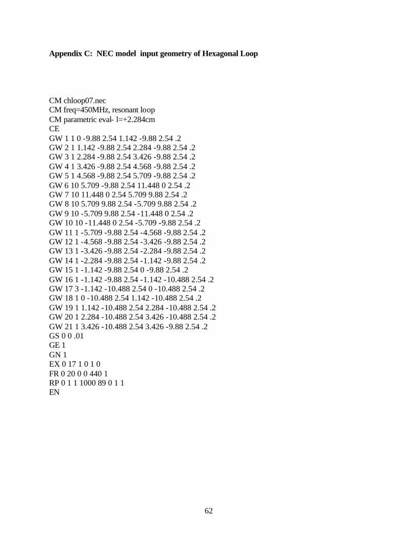
62
Appendix C: NEC model input geometry of Hexagonal Loop CM chloop07.nec CM freq=450MHz, resonant loop CM parametric eval- l=+2.284cm CE GW 1 1 0 -9.88 2.54 1.142 -9.88 2.54 .2 GW 2 1 1.142 -9.88 2.54 2.284 -9.88 2.54 .2 GW 3 1 2.284 -9.88 2.54 3.426 -9.88 2.54 .2 GW 4 1 3.426 -9.88 2.54 4.568 -9.88 2.54 .2 GW 5 1 4.568 -9.88 2.54 5.709 -9.88 2.54 .2 GW 6 10 5.709 -9.88 2.54 11.448 0 2.54 .2 GW 7 10 11.448 0 2.54 5.709 9.88 2.54 .2 GW 8 10 5.709 9.88 2.54 -5.709 9.88 2.54 .2 GW 9 10 -5.709 9.88 2.54 -11.448 0 2.54 .2 GW 10 10 -11.448 0 2.54 -5.709 -9.88 2.54 .2 GW 11 1 -5.709 -9.88 2.54 -4.568 -9.88 2.54 .2 GW 12 1 -4.568 -9.88 2.54 -3.426 -9.88 2.54 .2 GW 13 1 -3.426 -9.88 2.54 -2.284 -9.88 2.54 .2 GW 14 1 -2.284 -9.88 2.54 -1.142 -9.88 2.54 .2 GW 15 1 -1.142 -9.88 2.54 0 -9.88 2.54 .2 GW 16 1 -1.142 -9.88 2.54 -1.142 -10.488 2.54 .2 GW 17 3 -1.142 -10.488 2.54 0 -10.488 2.54 .2 GW 18 1 0 -10.488 2.54 1.142 -10.488 2.54 .2 GW 19 1 1.142 -10.488 2.54 2.284 -10.488 2.54 .2 GW 20 1 2.284 -10.488 2.54 3.426 -10.488 2.54 .2 GW 21 1 3.426 -10.488 2.54 3.426 -9.88 2.54 .2 GS 0 0 .01 GE 1 GN 1 EX 0 17 1 0 1 0 FR 0 20 0 0 440 1 RP 0 1 1 1000 89 0 1 1 EN

63
References 1. W.L. Pritchard, J.A. Sciulli, Satellite Communications Systems Engineering, Prentice-
Hall, 1998 2. W.L. Stutzman, G.A. Thiele, Antenna Theory and Design, 2nd edition, Wiley and Sons:
1998 3. C.A. Balanis, Antenna Theory and Design, Wiley and Sons: NY, 1982
4. R.C. Johnson, Antenna Engineering Handbook, 3rd edition, McGraw-Hill 5. W.L. Stutzman, Polarization in Electromagnetic Systems, Artech House, Canton, Mass, 1993 6. K.F. Lee, W.Chen, Advances in Microstrip and Printed Antennas, Wiley and Sons: NY,
1997 7. D.R. Jackson & N.G. Alexopoulos, “Simple Approximate Formulas for Input Resistance,
Bandwidth and Efficiency of a Resonant Rectangular Patch, IEEE Transactions on Antennas and Propagation, Vol 39, No 3, March 1991 pgs 407-410.
8. Mehmet Kara, “A Simple Technique for the Calculation of the Bandwidth of Rectangular
Microstrip Antenna Elements with Various Substrate Thicknesses” Microwave and Optical Technology Letters / Vol 12, No. 1, May 1996 pgs 16-20.
9. S.H. Al-Charchafci, W.K. Won Ali, S. Sinkeree, “A Stacked Annular-Ring Microstrip
Patch Antenna”, IEEE APS Symposium, July 1997, pg 948-951 10. J.R. James, A. Henderson, P.S. Hall, “Microstrip Antenna Performance Is Determined by
Substrate Constraints”, MSN, August 1982, pg 73-84 11. C.C. Kilgus, “Resonant Quadrifilar Helix” IEEE Transactions, Vol AP-17, May 1969,
pgs 349-351 12. Richard Johnson & Henry Jasik, “Antenna Applications Reference Guide” McGraw-Hill,
NY, 1987 13. Leon W. Couch, III, Digital and Analog Communication Systems, 6th ed., Prentice-Hall, 2001, pgs 338-351 14. M.W. Maxwell, Reflections-Transmission Lines and Antennas, ARRL, 1990 15. J.J. Carr, Loop Antenna Handbook, Universal Radio Research, 1999 16. The ARRL Antenna Book 18th ed., ARRL, Newington CT, 1997

64
17. R.L. Thomas, A Practical Introduction to Impedance Matching, Artech House, 1976.
18. D.M. Pozar, Microwave Engineering, Addison-Wesley, 1990
19. R.W. Lewallen, “Baluns: What They Do and How They Do It”, The ARRL Antenna
Compendium, Vol 1, ARRL, Hartford Conn. 1985 20. J.E. Storer, Impedance of Thin Wire Loop Antennas, AIEE Trans. (Part 1. Comm and
Electronics) Vol. #75 November 1956, pg 606-619
21. R. King, “Theory of Antennas Driven from Two Wire Line”, Journal of Applied Physics, Vol. #20, 1949, pg 832
22. A. Richtscheid, “Calculation of the Radiation Resistance of Loop Antennas with
Sinusoidal Current Distribution”, IEEE Transactions on Antennas and Propagation, Vol #AP 24, No. 6, Nov 1976, pg 889-891
23. RWP King, “Theory of the Center Driven Square Loop Antenna” IRE Transactions on
Antennas and Propagation, Vol AP-4, No 4, July 1956, pg 393
24. T. Tsukiji & S. Tou, “On Polygonal Loop Antennas”, IEEE Transactions on Antennas and Propagation, Vol AP-28, No 4, July 1980, pg 571-575

65
Vita
Christian W. Hearn, P.E., was born on February 25, 1966 in Norfolk Virginia. He received a B.S. in Mechanical Engineering from Virginia Tech in 1989. From 1989 to 1997 he worked for the Underwater Explosions Research Division of the Naval Surface Warfare Center. During his employment, he completed a second B.S. in Electrical Engineering Technology at Old Dominion University. He is currently pursuing a Ph.D. in Electrical Engineering at Virginia Tech. His research interests include antenna design, testing, and measurements.