efficient modeling and floorplanning of …cas.ee.ic.ac.uk/people/schaudhu/fparticle.pdf ·...
TRANSCRIPT

EFFICIENT MODELING AND FLOORPLANNING OF EMBEDDED-FPGA FABRIC
Sumanta Chaudhuri, Jean-Luc Danger, Sylvain GuilleyGET / Telecom Paris, CNRS – LTCI (UMR 5141)46 rue Barrault, 75634 PARIS Cedex 13, FRANCE
ABSTRACTIn this paper we present an automatic design flow for gen-erating customized embedded FPGA (eFPGA) fabric anda domain specific SOC+eFPGA architecture. This designflow encompasses both the eFPGA user and automatic lay-out generator perspectives. We discuss generic FPGA mod-eling based on VPR, simulation and high-level models ofreconfigurable components, and we present an innovativefloor-planing for island style FPGAs using rectilinear macros.Several system integration issues are highlighted. Layout ofa real life SOC with an embedded RTR FPGA for crypto-graphic applications, designed with this flow, is also pre-sented.
1. INTRODUCTION
Rapid evolution in technology permits us to use program-able parallel devices along with microprocessors in a SOC.While eFPGAs are flexible, and reasonably fast comparedto serially executed microprocessor code, it also presentsa huge cost in area compared to application specific hardIPs. Due to these factors, it’s vital to have an efficient floor-plan and timing budget for these programable fabrics, whichshould be optimum in area and delay.
Several companies have already come up with program-able logic fabric [1, 2], but in most cases users can not cus-tomize the fabric according to their own needs. The prob-lems associated with customized programable logic coresare well summarized by Wilton et. al [3]. While [3] pro-poses a soft PLC approach, that is the fabric synthesized asstandard cell design, and can be customized by the user [4],discusses the problems of synthesizing an FPGA due to ahuge number of potential timing paths. Hauck [5, 6] pro-poses an architecture called “Rapid” and an automatic gen-erator of layout called “Totem”. An automatic layout gener-ator is proposed by Kuon et. al [7]. Our CAD flow consistsin integrating the bitstream and the structural VHDL gener-ator into the place and route tool vpr [8], instead of usinga seperate tool. Our eFPGA architecture differs from theabove mentioned architectures in
• While most other architectures propose a course grainreconfigurable fabric, somewhere in between a stan-dard FPGA [5] and a ASIC, to compensate for the
area and delay cost, we plan to implement a standardFPGA embedded in a SOC aimed at random logic,and modeled with VPR [8], (an open source FPGAmodeling and place/route tool developed at universityof Toronto).
• Our architecture is oriented towards run-time Recon-figurability and a multi-tasking FPGA.
These basic differences are reflected in the design flow thatwe are going to present.
The rest of the article is organized as follows: In sec-tion 2 we present the generic eFPGA design flow and aoverview of the domain sepcific eFPGA, section 3 presentsmodeling and simulation of reconfigurable components, insection 4 we present a physical layout of FPGA using rec-tilinear macros, section 5 presents system integration issuesand in section 6 we present an eFPGA designed with thisflow.
2. OVERVIEW
2.1. Design Flow
Our FPGA design flow as illustrated in figure 1, has a sin-gle entry point: namely the architecture file (format VPR).To fully exploit the capabilities of VPR as a FPGA mod-eling tool, and not as a mere Placer/Router, VPR has beenmodified to generate a VHDL structural model as a one toone mapping from it’s internal routing graph. The advan-tage of this flow is, that since the place/route and modelinguse the same structure, the bitstream and physical layout isalways coherent, and complicated modeling issues such asstaggered segments, different types of switch-boxes are al-ready taken care of by VPR.
The design flow can be viewed from two perspectivesas explained in figure 1: user and the designer. They sharethe same modeling software(VPR) and the same architec-ture file. A domain-specific user proceeds to design hisSOC with the help of VPR, which allows him to explore thedesign-space, and RTL models, which allows him to rapidlysimulate his dynamic reconfiguration strategies. Once a suit-able architecture is determined depending on the area/timeconstraints in his SOC, he passes on the architecture fileand the timing constraints to the FPGA fabric designer. The

LEGEND EQUIVALENTFLOW
VPRARCHITECTURE FILE
COMPONENTLIBRARYsynthesis
DESIGNERPERSPECTIVE
VPRASIC Tools+EFPGA Fabri Designer
AUTOMATIC FLOORPLANPLACE/ROUTE (SILICON)CLOCK TREE LAYOUTTIMING VERIFICATIONDRC + LVS
USERPERSPECTIVE
Bitstream
MASK DELAY ABSTRACTTIMING
Mask+Layout Abstra t+Timing Abstra tAr hite ture File + Expe ted Timing
Simulation ToolsVPR++Domain Knowledge
Domain Spe ifi User
ROUTING GRAPH
VHDL SIMULATORBitstreamRTL
VHDL SIMULATORBitstreamIn Cir uit Simulation
Fun tional Simulation( lbs ,
Bitstream
NetlistBa k Annotate DelayBa k Annotate Faults
MODELSswit hes)
SDF AnnotatePLACER/ROUTER(FPGA)
STRUCTURAL VHDL
Fig. 1. Domain Specific EFPGA Fabric Design Flow
FPGA designer can rapidly generate a structural VHDL andan automatic floorplan from this architecture file, and pro-vides the mask, the layout and timing abstracts to the domainspecific user, which are essential for integration of the eF-PGA into SOC. Depending on the design complexity theremight be a few iterations of the above transactions.
The input to the automatic layout generator is the struc-tural VHDL generated by VPR, so it can handle FPGAs thatcan be modeled with VPR.
2.2. VHDL Model
The structural VHDL model describes the connectivity tothe layout tool, and thus describes the bitstream ordering.The automatic layout generator uses this VHDL structureand generic parameters from the architecture file to repeatthe same motif (i.e the configurable tile CT which consists ofCLB and connection boxes, and the switchbox) over space.The switchbox and connection box interconnections are de-scribed in VHDL. This model can also be laid out as a flatstandard cell design, however in that case we won’t be re-specting the structure assumed by VPR timing analyzer.
Although this structural description doesn’t need any syn-thesis, a synthesis tool is important for detecting timing vi-olations that may occur for configuration signals w.r.t con-figuration clock. To have a correct timing analysis, we dis-able all functional paths (i.e paths corresponding to inter-connect resources are set as false paths) and the synthesizeranalyzes only the paths that are relevant for correct configu-
ration. The functional timing analysis inside FPGA is donepost-fabrication with the FPGA place/route tool (i.e VPR).This issue is discussed in detail in section 5.
3. SIMULATION AND MODELING OF BASICCOMPONENTS
The basic components of our FPGA are CLB configurablelogic block (4-LUT+FF), the switches(tri-state buffer, trans-mission gates, muxes) and the configuration points, whichin our case are Flip-Flops connected in a shift register chain.Apart from the transmission gates, all other components aresynthesized as a standard-cell design, thus we used the ven-dor provided models to simulate them. We are going to dis-cuss in detail the simulation and modeling of transmissiongates.
3.1. Pass Transistor and Transmission Gate
Pass transistors are frequently used in modern day FPGAsand reconfigurable architectures. Aside from the fact, thatthey are more compact compared to tri-state buffer switches,they are also bi-directional. Considerable Research has beendone on pass-transistor dimensions notably by Betz et al [9,10]. However few references are available on the topic ofpass-transistor modeling. Such a model seems necessary forRTR FPGAs to avoid potential short-circuits, and for valida-tion at the early steps of the design flow, (i.e simulation withbehavioural models of other co-systems) without going into

S: Column[1℄ D:Column[4℄Pro essENVIRONMENT test D
STATE=ONS'driving value: Column[2℄
D'driving value: Column[3℄test S ENVIRONMENT
test S test D ns Æ 1 2 3 40 Z 0 +0 U Z Z U0 Z 0 +1 0 Z 0 Z0 Z 0 +2 0 Z 0 01 Z 10 +0 1 Z 1 01 Z 10 +1 1 Z 1 1Z 1 20 +0 Z 1 Z 1Z 1 20 +1 1 1 Z 11 Z 30 +0 1 Z 1 Z1 Z 30 +1 1 Z 1 10 1 40 +0 0 Z 0 10 1 40 +1 0 X 0 X0 1 40 +2 X X Z X0 1 40 +3 X 1 Z 11 0 50 +0 1 0 Z 01 0 50 +1 X 0 X 01 0 50 +2 X Z X X1 0 50 +3 1 Z 1 XZ H 60 +0 Z Z Z XZ H 60 +1 1 H Z HZ H 60 +2 H H Z HZ L 70 +0 H L Z LZ L 70 +1 L L Z LFig. 2. Pass transistor model: simulated values
spice simulations which are too slow.The Major disadvantage with pass-transistor gates is that
it’s output voltage can only rise to Vdd − Vt [9]. The trans-mission gate circumvents this problem at the cost of 1 moretransistor of opposite polarity.
3.2. Transmission Gate Model
In this section we present a transmission gate model whichallows rapid simulation and functional verification of theFPGA run-time reconfiguration strategies. In figure 2 wedepict the behaviour of this model. Either of the pins Dor S can be source or sink over time. We always write aweak value(’Z’) to the source and the resolved value of thesource to the sink. Each time the process is called (i.e. foreach delta D or S changes value). Delta refers to the sym-bolic time for process execution. We test if the driving valueis different from resolved value, to identify the source andthe sink, and act accordingly. If the driving value is differ-ent from the resolved value, then it is source, otherwise itis sink, since sink does not drive any value into the port.Pseudo code of the process is given below:
process(d,s)
beginif((d=d’driving_value and s=s’driving value) or(d/=d’driving_value and s/=s’driving value)) then
d<= s;s<= d;
elseif(d’event and d/=d’driving value) then 10
s<=d;
elsif(d’event and d=d’driving value) thens<=’Z’;
end if;
if(s’event and s/=s’driving value) thend<=s;
elsif(s’event and s=s’driving value) thend<=’Z’;
end if; 20end if;
end process;
4. PHYSICAL LAYOUT
4.1. Rectilinear Modules
An efficient and compact layout of the FPGA is essential.The advantages of using rectilinear macros are described infigure 3. In a conventional layout we are constrained to haverectangular shapes aligning with other rectangular shapes,even if a module is not very dense(e.g a particular connec-tion box does not have a many switches but it must alignwith other modules). However in rectilinear layout the stan-dard cells from both CLB and connection boxes are evenlyspread out. Moreover, since in our architecture each CLBwith it’s connection boxes belongs to the same reconfig-urable entity(i.e same address) this rectilinear tile permitsus to use a modular and repetitive layout.
4.2. Automatic Floorplan
Our layout scheme is divided in two parts. Firstly the rout-ing matrix which consists of square switch-boxes and rout-ing channels repeated over space, and secondly the rectilin-ear Configurable Tiles (CLB + Connection Boxes) superim-posed on this routing matrix. The automatic layout genera-tor in figure 1 works in the following manner
• First the switches inside the switchboxes are placedand routed and a switchbox library is built. 9 dif-ferent switchbox types (4 side +4 corner +centre) areplaced and routed. We use the same size for all ofthem because the FPGA area is mainly dependent on
������
������
������
������
��������
��������
��������
��������
������
������
������
������
������
������
������
������
������
������
������
������
������
������
������
������
��������
��������
������
������
������
������
������
������
��������
��������
������
������
������
������
����������������
����������������
������
������
������
������
������
��������������
��������
������
������
������
������
��������
������
������
������
������
��������
������
������
��������
��������
������
������
������
������
������
������
������
������
������
������
��������
��������
��������
������
��������������
��������
��������
��������
��������
������
������
������
������
������
������
������
������
��������
��������
��������
��������SBOXCLBCBOX2
Re tangular Re tilinear
SBOXCTCBOX1Fig. 3. Rectangular Vs. Rectilinear

Fig. 4. Rectilinear Configurable Tile (CT)
Fig. 5. FPGA layout
the centre switch box size. The routing channel portsare aligned for each switch box. These switchboxesare then placed inside FPGA.
• Next the CTs as described in figure 4 are placed androuted. Their rectilinear dimensions are dependent onswitchbox dimensions previously calculated. Thereare 5 different CTs( 4 side + Centre) as shown in fig-ure 5.
• clock tree synthesis: To insert the clock tree bufferswe left small slices in between the configurable tilesand switchboxes. This slice size is estimated in twopass. For the first pass all tiles are placed, and clocktree is synthesized. In the next pass all tiles are re-placed with appropriate gaps between them, to insertclock tree buffers.
• The configuration signals are routed automatically byASIC layout tool in the top metal layers
5. SYSTEM INTEGRATION
5.1. Timing Abstract Generation of eFPGA
Generating a timing and layout abstract of the eFPGA is likethe data-sheet of a conventional FPGA. Automatic timinganalyzers consider all possible paths in a design, to deter-mine the critical path. Obviously in an FPGA all paths are
not of interest, e.g the paths from configuration input sig-nals to the functional outputs. Another example is a path inthe FPGA which includes all the switches, since we are notgoing to program the FPGA in such a manner. So the fol-lowing method has been used to generate the timing abstractof the EFPGA.
• First we fix the critical path delay tcrit inside the FPGA.This depends on the period of the clock signal used inSOC(tcrit = tclk soc). This must be compared before-hand with the timings of a set of benchmark circuitsplaced/routed in FPGA. In our case the clock periodis 15 ns. We also fix the maximum input delay for allinput pins, and maximum output delay for all outputpins.
• While generating the timing abstract, we disable allfunctional paths inside the FPGA, and all paths be-tween configuration and functional signals.
• For each functional inputs we add only one path toeach of the outputs with a delay tcrit.
• All the configuration signals are synchronous, so theyare not disabled, and we specify the transition time foreach signal.
• We include the clock insertion delay in the timing ab-stract, which is necessary for clock tree generation atthe top level.
The timing abstract permits the ASIC timing analyzer to op-timize the critical paths that are partly inside the FPGA andpartly in SOC. The value tcrit is then passed on to FPGAplace/route and timing analyzer tool(VPR) which guaran-tees this delay inside FPGA.
5.2. Interface
During Boot process the eFPGA is unprogrammed. Un-known values for critical output signals connected to theinterfacing circuitry, might cause a failure during boot pro-cess(e.g a interrupt line is asserted). To avoid that, at Power-on-Reset every output signal is disconnected from the inter-nal cells of eFPGA, and pulled up/down to a known value.During normal operation these outputs must be reprogrammedto their original functionality.
6. REALISATION
6.1. Architecture and Layout Summary
Our SOC architecture is based upon an open source micro-processor(FREE6502), and several cryptographic IPs resis-tant against side channel attacks. It also includes a dynam-ically reconfigurable FPGA code named FASE. The system
FREE6502
DES
CRYPTOIP 1VCI INTERFACEVCI WRAPPERVCI INTERFACEVCI WRAPPER
VCI WRAPPER VCI INTERFACEVCI WRAPPER VCI INTERFACEVCI WRAPPER
CONFSIGNALSFASE CONFVCI INTERFACEVCI WRAPPER
VCI INTERFACECRYPTOIP 2
FASE ARRAY
Fig. 6. System Overview
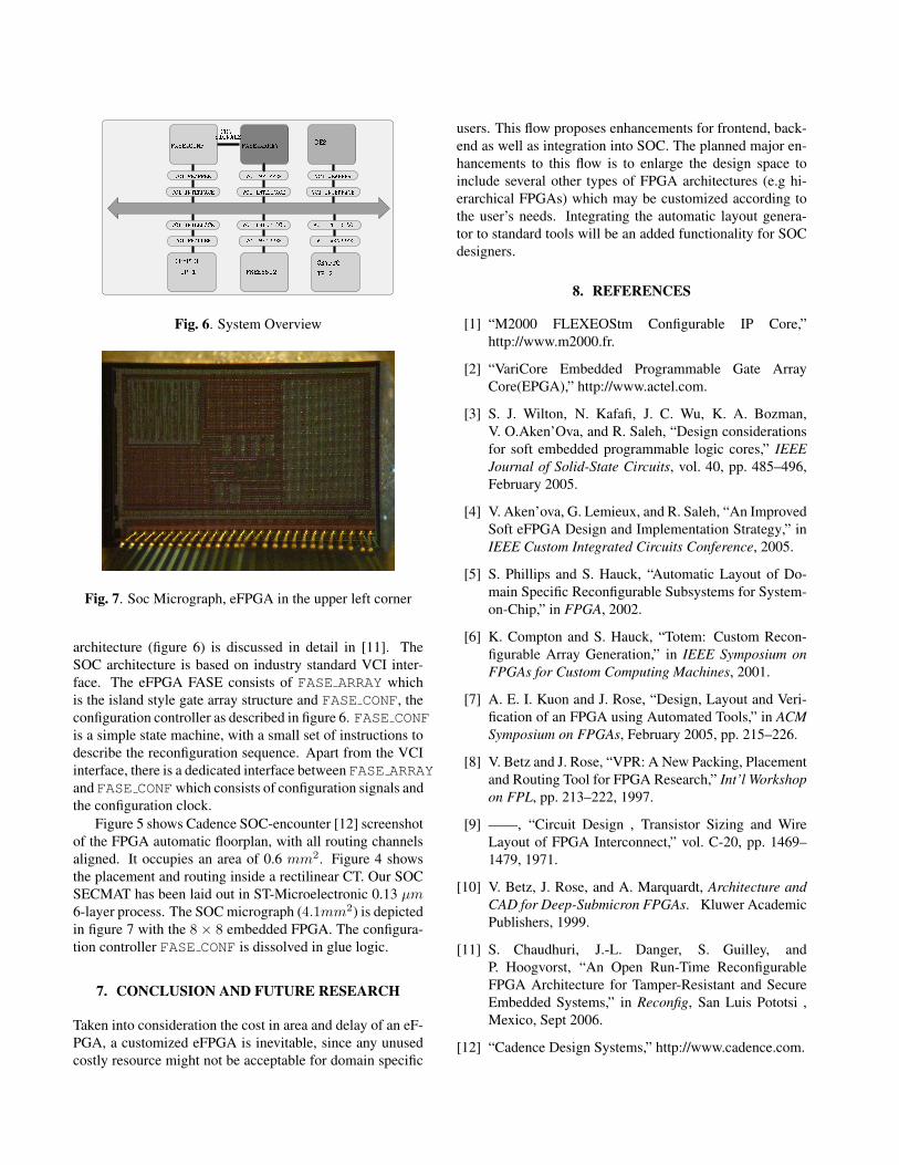
Fig. 7. Soc Micrograph, eFPGA in the upper left corner
architecture (figure 6) is discussed in detail in [11]. TheSOC architecture is based on industry standard VCI inter-face. The eFPGA FASE consists of FASE ARRAY whichis the island style gate array structure and FASE CONF, theconfiguration controller as described in figure 6. FASE CONFis a simple state machine, with a small set of instructions todescribe the reconfiguration sequence. Apart from the VCIinterface, there is a dedicated interface between FASE ARRAYand FASE CONFwhich consists of configuration signals andthe configuration clock.
Figure 5 shows Cadence SOC-encounter [12] screenshotof the FPGA automatic floorplan, with all routing channelsaligned. It occupies an area of 0.6 mm2. Figure 4 showsthe placement and routing inside a rectilinear CT. Our SOCSECMAT has been laid out in ST-Microelectronic 0.13 µm6-layer process. The SOC micrograph (4.1mm2) is depictedin figure 7 with the 8 × 8 embedded FPGA. The configura-tion controller FASE CONF is dissolved in glue logic.
7. CONCLUSION AND FUTURE RESEARCH
Taken into consideration the cost in area and delay of an eF-PGA, a customized eFPGA is inevitable, since any unusedcostly resource might not be acceptable for domain specific
users. This flow proposes enhancements for frontend, back-end as well as integration into SOC. The planned major en-hancements to this flow is to enlarge the design space toinclude several other types of FPGA architectures (e.g hi-erarchical FPGAs) which may be customized according tothe user’s needs. Integrating the automatic layout genera-tor to standard tools will be an added functionality for SOCdesigners.
8. REFERENCES
[1] “M2000 FLEXEOStm Configurable IP Core,”http://www.m2000.fr.
[2] “VariCore Embedded Programmable Gate ArrayCore(EPGA),” http://www.actel.com.
[3] S. J. Wilton, N. Kafafi, J. C. Wu, K. A. Bozman,V. O.Aken’Ova, and R. Saleh, “Design considerationsfor soft embedded programmable logic cores,” IEEEJournal of Solid-State Circuits, vol. 40, pp. 485–496,February 2005.
[4] V. Aken’ova, G. Lemieux, and R. Saleh, “An ImprovedSoft eFPGA Design and Implementation Strategy,” inIEEE Custom Integrated Circuits Conference, 2005.
[5] S. Phillips and S. Hauck, “Automatic Layout of Do-main Specific Reconfigurable Subsystems for System-on-Chip,” in FPGA, 2002.
[6] K. Compton and S. Hauck, “Totem: Custom Recon-figurable Array Generation,” in IEEE Symposium onFPGAs for Custom Computing Machines, 2001.
[7] A. E. I. Kuon and J. Rose, “Design, Layout and Veri-fication of an FPGA using Automated Tools,” in ACMSymposium on FPGAs, February 2005, pp. 215–226.
[8] V. Betz and J. Rose, “VPR: A New Packing, Placementand Routing Tool for FPGA Research,” Int’l Workshopon FPL, pp. 213–222, 1997.
[9] ——, “Circuit Design , Transistor Sizing and WireLayout of FPGA Interconnect,” vol. C-20, pp. 1469–1479, 1971.
[10] V. Betz, J. Rose, and A. Marquardt, Architecture andCAD for Deep-Submicron FPGAs. Kluwer AcademicPublishers, 1999.
[11] S. Chaudhuri, J.-L. Danger, S. Guilley, andP. Hoogvorst, “An Open Run-Time ReconfigurableFPGA Architecture for Tamper-Resistant and SecureEmbedded Systems,” in Reconfig, San Luis Pototsi ,Mexico, Sept 2006.
[12] “Cadence Design Systems,” http://www.cadence.com.