effect of pixel size and scintillator on image quality - worcester
TRANSCRIPT

EFFECT OF PIXEL SIZE AND SCINTILLATOR ON IMAGE QUALITY OF A CCD-BASED DIGITAL X-RAY
IMAGING SYSTEM
By
Michael J. Leal
A Thesis
Submitted to the Faculty
of the
WORCESTER POLYTECHNIC INSTITUTE
in partial fulfillment of the requirements for the
Degree of Master of Science
in
Biomedical Engineering
May 2001
APPROVED: Andrew Karellas, Ph.D., Major Advisor Professor, Department of Radiology University of Massachusetts Medical School Robert A. Peura, Ph.D., Co-Advisor Professor Biomedical Engineering Department, WPI Christopher H. Sotak, Ph.D., Co-Advisor Professor and Department Head Biomedical Engineering Department, WPI

i
Abstract
The term “Digital X-ray Imaging” refers to a variety of technologies that
electronically capture x-ray images. Once captured the images may be electronically
processed, stored, displayed and communicated. Digital imaging has the potential to
overcome weaknesses inherent in traditional screen-film imaging, with high detection
efficiency, high dynamic range and the capability for contrast enhancement. Image
processing also makes possible innovative techniques such as computer-aided
diagnosis, tomosynthesis, dual-energy imaging, and digital subtraction imaging.
Several different approaches to digital imaging are being studied, and in some cases,
have been developed and are being marketed. Common to all these approaches are a
number of technological and medical issues to be resolved. One of the technological
issues is the optimal pixel size for any particular image sensor technology. In
general, the spatial resolution of the digital image is limited by the pixel size.
Unfortunately while reducing pixel size improves spatial resolution this comes at the
expense of signal to noise ratio (SNR). In a scintillator-charge-coupled device (CCD)
system, the signal can be increased by improving the efficiency of the scintillator or
by reducing noise. This study used a very low noise CCD to determine if image
quality, as indicated by the modulation transfer function (MTF), the noise power
spectrum (NPS) and the detective quantum efficiency (DQE), could be maintained
while reducing pixel size. Two scintillators, one a commonly used radiographic
screen the other a thallium doped cesium iodide scintillator, were used and the results
compared. The results of this study show that image quality can be maintained as
pixel size is reduced and that high DQE can be attained and maintained over a wide
range of spatial frequencies with a well designed scintillator.

ii
ACKNOWLEDGMENTS
Mr. Leal wishes to acknowledge the assistance of the following people: teachers, colleagues and friends. I would like to thank my major advisor, Dr. Andrew Karellas, for his extraordinary knowledge, patience, and encouragement. His suggestions were invaluable and to him I extend my heartfelt gratitude. I am grateful for the academic advice and encouragement provided by Dr. Robert Peura, and his unceasing willingness to answer questions throughout my tenure as a student at WPI. I also appreciate the support of Dr. Christopher Sotak as a co-advisor. I would also like to thank Srinivasan Vedantham and Sankararaman Suryanarayanan for sharing their expertise, and humor. A special thanks to my wife, Cynthia, for her support, understanding and love. I would not be where I am today without her.

iii
TABLE OF CONTENTS
ABSTRACT i
ACKNOWLEDEMENTS ii
I. INTRODUCTION 1
II. METHODS AND MATERIALS 9
A. Equipment 9
B. Presampling modulation transfer function measurement 12
C. Noise power sprectrum (NPS) measurement 15
D. NEQ and DQE measurement 22
III. RESULTS 24
A. Presampling MTF 24
B. NPS 29
C. NEQ 38
D. DQE 46
IV. DISCUSSION 53
V. CONCLUSION 55
VI. REFERENCES 57
APPENDIX A – SUPPLEMENTAL FIGURES 60

iv
LIST OF FIGURES
Figure 1. Schematic of a Scintillator-CCD Detector. Incident X-ray photons interact with the scintillator where they are absorbed and light photons are emitted. Light photons enter the fiberoptic plate and are carried to the CCD where they are detected and converted to electrons. 2
Figure 2. Hardware binning process 6
Figure 3. Experimental setup for MTF measurement 13
Figure 4. 2-D NPS for Kodak MIN-R 2000™ (left) and CsI (right) scintillators. Both images were derived from 16 images with no binning (24 micron pixels) with 5 mAs exposures. 17
Figure 5. Experimental setup for NPS measurement 20
Figure 6. Presampling MTF for Kodak MIN-R 2000™ scintillator for 24 micron (unbinned), 48 micron, 72 micron and 96 micron pixel sizes through hardware binning. 25
Figure 7. Presampling MTF for CsI:Tl scintillator for 24 micron (unbinned), 48 micron, 72 micron and 96 micron pixel sizes through hardware binning. pixel sizes through hardware binning. 26
Figure 8. Comparison of MTF with Kodak MIN-R 2000™ and CsI:Tl, with no binning (24 micron). Above 3 cycles/mm the CsI:Tl MTF is greater than the Kodak MIN-R 2000™ MTF and the CsI:Tl MTF is greater than 0.1 up to 13.5 cycles/mm while the Kodak MIN-R 2000™ MTF drops below 0.1 at 9.5 cycles/mm. 27
Figure 9. Comparison of MTF with Kodak MIN-R 2000™ and CsI:Tl, with 4 x 4 binning (96 micron). Above 3 cycles/mm the CsI:Tl MTF is slightly greater than the Kodak MIN-R 2000™ MTF indicating that there may be a slight improvement in resolution when the CsI:Tl scintillator is used. 28
Figure 10. NPS at 5, 10, 16 and 20 mAs with Kodak MIN-R 2000™ with no binning (24 micron). As expected, the normalized NPS decreases as exposure increases. 30

v
Figure 11. NPS at 5, 10, 16 and 20 mAs with CsI:Tl with no binning (24 micron). As expected, the normalized NPS decreases as exposure increases. 31
Figure 12. NPS comparison of Kodak MIN-R 2000™ and CsI:Tl at 5 mAs with no binning (24 micron). CsI shows lower noise, particularly at low frequencies, than Kodak MIN-R 2000™. 32
Figure 13. NPS comparison of Kodak MIN-R 2000™ and CsI:Tl at 20 mAs with no binning (24 micron). CsI shows lower noise, particularly at low frequencies, than Kodak MIN-R 2000™. 33
Figure 14. NPS for Kodak MIN-R 2000™ at 5 mAs for 24 micron, 48 micron, 72 micron and 96 micron pixel sizes. NPS decreases slightly as pixel size increases reflecting the relative increase in signal. No significant improvement in noise is noted. 34
Figure 15. NPS for CsI:Tl at 5 mAs for 24 micron, 48 micron, 72 micron and 96 micron pixel sizes. As in the case of Kodak MIN-R 2000™, NPS decreases slightly as pixel size increases reflecting the relative increase in signal. No significant improvement in noise is noted. 35
Figure 16. Hardware vs Software 2 x 2 Binning (48 micron), NPS for Kodak MIN-R 2000™ at 5 mAs and 20 mAs. No significant difference is noted between hardware and software binning. 36
Figure 17. Hardware vs Software 2 x 2 Binning (48 micron), NPS for CsI:Tl at 5 mAs and 20 mAs. As with Kodak MIN-R 2000™, no significant difference is noted between hardware and software binning. 37
Figure 18. NEQ for Kodak MIN-R 2000™ with no binning at 5 mAs, 10 mAs, 16 mAs and 20 mAs. As expected, the NEQ increases with exposure. 39
Figure 19. NEQ for CsI:Tl with no binning at 5 mAs, 10 mAs, 16 mAs and 20 mAs. As with Kodak MIN-R 2000™, the NEQ increases with exposure. 40
Figure 20. NEQ for Kodak MIN-R 2000™ with 4 x 4 binning at 5 mAs, 10 mAs, 16 mAs and 20 mAs. As previously noted, the NEQ increases with exposure. 41
vi
Figure 21. NEQ for CsI:Tl with 4 x 4 binning at 5 mAs, 10 mAs, 16 mAs and 20 mAs. As with Kodak MIN-R 2000™, the NEQ increases with exposure. 42
Figure 22. NEQ for Kodak MIN-R 2000™ at 20 mAs (300170 quanta) for 24 micron, 48 micron, 72 micron and 96 micron pixels. The NEQ shows no significant difference as pixel size changes. 43
Figure 23. NEQ for CsI:Tl at 20 mAs (300170 quanta) for 24 micron, 48 micron, 72 micron and 96 micron pixels. The NEQ shows no significant difference as pixel size changes. 44
Figure 24. NEQ comparison of Kodak MIN-R 2000™ and CsI:Tl at 20 mAs for 1 x1 (24 micron) and 4 x 4 (96 micron) binning The NEQ for the CsI:Tl scintillator is consistently higher than for the Kodak MIN-R 2000™ scintillator. 45
Figure 25. DQE for Kodak MIN-R 2000™ without binning at exposures of 5 mAs, 10 mAs, 16 mAs and 20 mAs. There is minimal influence of exposure on DQE. 47
Figure 26. DQE for CsI:Tl without binning at 5 mAs, 10 mAs, 16 mAs and 20 mAs. As with Kodak MIN-R 2000™, there is minimal influence of exposure on DQE.. 48
Figure 27. DQE comparison of Kodak MIN-R 2000™ and CsI:Tl without binning at exposures of 5 mAs and 20 mAs. Not only is the DQE of the CsI:Tl initially higher than that of the Kodak MIN-R 2000™, it remains relatively high and does not begin to drop off until it reaches 10 cycles/mm. While the DQE for the Kodak MIN-R 2000™ falls below 0.1 at 9.5 cycles/mm, the DQE for the CsI:Tl does not drop below 0.1 until 19 cycles/mm. 49
Figure 28. DQE for Kodak MIN-R 2000™ with and without binning at 5 mAs. Other than limiting spatial resolution, pixel size does not influence the DQE in this system. 50
Figure 29. DQE for CsI:Tl with and without binning at 5 mAs. Other than limiting spatial resolution, pixel size does not influence the DQE in this system. 51

1
I. INTRODUCTION
The term “Digital X-ray Imaging” refers to a variety of technologies that
electronically capture x-ray images. Once captured the images may be electronically
processed, stored, displayed and communicated. Images may also be printed on film
for viewing and storage.
The first step in digital imaging is image acquisition. Traditionally image acquisition
has been accomplished using a fluorescent screen and film. This screen-film
technology and associated film processing have advanced in recent years and
specialized screens and films have been developed for particular imaging specialties
such as mammography1. While image quality has improved, screen-film technology
has significant limitations with respect to dynamic range, granularity and contrast.
Digital imaging has the potential to overcome these weaknesses with high detection
efficiency, high dynamic range and the capability for contrast enhancement. Image
processing also makes possible innovative techniques such as computer aided
diagnosis2, 3, tomosynthesis4, dual-energy imaging5, and digital subtraction imaging6.
Several different approaches to digital imaging are being studied, and in some cases,
have been developed and are being marketed. Techniques being studied include
dedicated detectors, which may be stationary or slot scanned, and removable
stimulable phosphor plates7 (CR plates), which are similar in appearance and use to
current screen-film cassettes. Dedicated detectors may be either direct detection,

2
such as amorphous selenium8, 9, 10 or CdZnTe, or indirect detection, using a
scintillator to convert x-rays to light and a light sensitive detector such as an active
matrix flat-panel imager (AMFPI)11, 12 or a charge-coupled device (CCD)13, 14 to
detect the light. A schematic of a scintillator-CCD system is shown in Figure 1.
Radiographic screens, such as Kodak MIN-R 2000, have been used as scintillators
as well as amorphous silicon and thallium doped cesium iodide (CsI:Tl).
Figure 1. Schematic of a Scintillator-CCD Detector. Incident X-ray photons interact with the scintillator where they are absorbed and light photons are emitted. Light photons enter the fiberoptic plate and are carried to the CCD where they are detected and converted to electrons.
Among those commercially available are CR plates, amorphous silicon-based, flat-
panel detectors and scintillator-CCD systems. CR plates are in use in general
radiography15 while amorphous silicon is in use in mammography16, 17. In these cases
“full field” detectors have been developed, i.e. detectors comparable in size to their
screen-film counterparts. The commercial scintillator-CCD systems are used in small
field imaging for stereotactic localization and core biopsies18.
Incident X-rays
Scintillator
Fiberoptic Plate
CCD
0.15 mm
25 mm

3
Common to all these approaches are a number of technological and medical issues to
be resolved. One of the technological issues is the optimal pixel size for any
particular image sensor technology19, 20, 21. In general, the spatial resolution of the
digital image is limited by the pixel size. For a given detector technology the spatial
resolution is inversely proportional to the pixel size and is defined as the Nyquist
limit which states that the maximum resolution, R, is equal to the inverse of 2 times
the pixel size, x, in mm [ )*2(1 xR = ]. From this relationship, a system with a pixel
size of 96 microns has a Nyquist limit of 5.2 cycles/mm while a system with a pixel
size of 24 microns has a Nyquist limit of 20.8 cycles/mm. High resolution is
important in applications such as mammography where microcalcifications on the
order of tenths of a mm provide an early indication of cancer. However, this
improvement in spatial resolution comes at the expense of signal to noise ratio (SNR)
and as SNR degrades so does image quality.
In addition, other components of the system, such as the scintillator, also influence
the system resolution. The system resolution (RT) can be derived from the following
relationship:
RRRR nT
222
21
2
1...111 +++= (1)
where R1, R2, …, Rn represent the resolution of the various components in the
imaging chain. From this relationship, a scintillator with a spatial resolution of 20.8
cycles/mm, coupled with a CCD with a spatial resolution of 20.8 cycles/mm will

4
result in a system resolution of 14.7 cycles/mm. In current clinical systems, screen-
film mammography has spatial resolutions between 16 and 18 cycles/mm. Newer CR
systems and amorphous selenium flat-panel systems have spatial resolutions up to 10
cycles/mm, and small field CCD systems have spatial resolutions between 5 and 10
cycles/mm.
In a scintillator-CCD system, SNR can be increased by increasing the x-ray exposure,
by improving the efficiency of the scintillator or by reducing noise. Increasing x-ray
exposure is undesirable since this increases patient dose. Improving the efficiency of
the scintillator is possible, however, this must be accomplished without requiring
additional dose, and without introducing artifacts or otherwise degrading the final
image. Image degradation typically occurs as a thick scintillator causes greater light
diffusion, a condition in which the light produced from one interaction illuminates
several pixels of the detector.
Reducing noise, by using a very low-noise CCD, is also possible. Photon noise,
preamplifier noise and dark current noise are the three primary noise sources in a
CCD. Dark current is thermally generated charge which can be measured and
subtracted from data. There is a noise component of dark current that cannot be
isolated and this may influence SNR if the signal is very low. Preamplifier noise is
generated by the on-chip output amplifier and is also called read noise. By carefully
choosing operating conditions this can be reduced to a few electrons. Photon noise is
a fundamental property of the quantum nature of x-rays and light and is unavoidable.

5
The charge collected by a CCD exhibits a similar Poisson distribution as the incident
photons so the noise is equal to the square root of the signal. Photon noise is always
present in imaging systems and is simply the uncertainty of the data.
For very low-noise CCDs it is not known if image quality can be maintained while
reducing pixel size. It is generally assumed that image quality, as measured by the
detective quantum efficiency (DQE), will degrade as pixel size decreases thus
negating any gain in resolution21. The DQE is a comparison of the output signal to
noise ratio (SNRout) to the input signal to noise ratio (SNRin) and is equal to the
square of the SNRout divided by the square of the SNRin. Ideally the SNRout should
equal the SNRin so that the ideal DQE is equal to 1 at all frequencies. In reality the
SNRout is less than the SNRin so the DQE is always less than 1.
Another method of increasing SNR is pixel binning, which will henceforth be
referred to as “binning”. Binning is the process of combining charge from adjacent
pixels in a CCD prior to readout (hardware binning) or combining digital values from
adjacent pixels in an image (software binning). The process of hardware binning is
shown in Figure 2. During exposure each pixel accumulates charge (Figure 2A).
Without binning each pixel of the CCD is individually transferred to the serial
register, then to the summing well and read (Figure 2B). In this case, each pixel is
displayed individually in the final image. With binning adjacent pixels are
transferred into the serial register 2, 3 or 4 at a time (Figure 2C). They are then

6
transferred to the summing well 2, 3 or 4 at a time then read together (Figure 2D). In
the case of 2 x 2 binning, 4 adjacent pixels are summed,
Serial shift direction
Serial Register SummingWell
11 12 13 1421 22 23 2431 32 33 3441 42 43 44
CCD Pixels
A. Individual pixels accumulateelectrons during exposure.
1121
1222
1323
1424
Serial Register SummingWell
31 32 33 3441 42 43 4451 52 53 5461 62 63 64
CCD Pixels
C. Individual pixels are shifted to theserial register two at a time duringreadout in 2 x 2 binning mode.
11 12 13 14
Serial Register SummingWell
21 22 23 2431 32 33 3441 42 43 4451 52 53 54
CCD Pixels
B. Individual pixels are shifted tothe serial register and then to thesumming well during readout in1 by 1 (full field) mode.
1121
1222
13,1423,24
Serial Register SummingWell
31 32 33 3441 42 43 4451 52 53 5461 62 63 64CCD Pixels
D. The serial register is shifted tothe summing well two at a timeduring readout in 2 x 2 binningmode.
Para
llel s
hift
dire
ctio
n
Figure 2. Hardware binning process. A. During exposure, individual pixels accumulate electrons in proportion to the light photons they detect. B. During readout, each row of pixels is shifted to the serial register, then each cell of the serial register is shifted to the summing well where it is read out. After all the serial register cells are read the next row of pixels is shifted into the serial register. C. For 2 x 2 binning, 2 rows of pixels are shifted to the serial register where they are summed. D. Two cells of the serial register are then shifted to the summing well, where they are

7
summed, and read out. After all the serial register cells are read the next 2 rows of pixels is shifted into the serial register.
the sum is then processed and displayed as a single pixel in the final image. If the
CCD has 24 micron pixels then 2 x 2 binning will yield an effective pixel size of 48
microns. Similarly, 3 x 3 binning will yield an effective pixel size of 72 microns and
4 x 4 binning will yield an effective pixel size of 96 microns.
One limitation of hardware binning is saturation, the point at which a pixel, the serial
register or the summing well reaches its capacity. When saturation occurs any charge
beyond the saturation value will be truncated and the final image will reflect the
maximum pixel value rather than the actual value. An even greater problem is
degradation of contrast due to charge spilling to adjacent pixels. Since 4, 9 or 16
individual pixels may be summed in the summing well its capacity may be exceeded
during the binning process even though the individual pixels have not reached
saturation. If this occurs, software binning may be a suitable option.
A comparison of full-field digital mammography (FFDM) with screen-film
mammography, a procedure dependent on high resolution and high image quality,
showed no difference in cancer detection rate22. The FFDM system used an
amorphous silicon area detector bonded to a cesium iodide crystal (GE Medical
Systems) with a pixel size of 100 microns. This limited the spatial resolution of the
FFDM system to 5 cycles/mm compared to spatial resolutions between 16 and 18
cycles/mm for current screen-film mammography systems. In order for digital x-ray

8
imaging to achieve it’s potential, and exceed comparable screen-film procedures, the
limiting spatial resolution must be increased and this must be accomplished without
degrading image quality.
This study compares the effect of pixel size and scintillator on image quality of a
CCD based digital imaging system. The modulation transfer function (MTF), noise
power spectrum (NPS), and detective quantum efficiency (DQE) are used as
indicators of image quality. The study was conducted using two different
scintillators, one designed as a screen for screen-film mammography, and one
designed as a scintillator for use with a CCD. A very low-noise CCD with a 24
micron pixel pitch and with binning capability was used. Both hardware and software
binning techniques were used to obtain pixel sizes of 48, 72 and 96 microns.

9
II. METHODS AND MATERIALS
A. Equipment
For this study a “SciTe”, Photometrics, Inc., Tucson, AZ, calibrated 1024 x 1024
pixel (24 µm x 24 µm) CCD was used. This CCD has a 100% fill factor, meaning
that the entire area of each pixel is active and can accumulate charge. The CCD is
also fully binnable, i.e. the pixels can be read individually or in groups. The CCD is
back illuminated, meaning that the image is focused on the backside of the CCD
where there is no gate structure. This gives the CCD high sensitivity to light from the
soft x-ray to the near infrared regions of the spectrum. The CCD has thermoelectric
cooling with a liquid circulation chiller and thermal isolation around the CCD. The
CCD was operated between –25o C and –35o C resulting in a dark current between
12.6 electrons/pixel/second and 6 electrons/pixel/second. Read noise for this CCD is
10 electrons rms or better.
The CCD is bonded to a fiberoptic plate approximately 1 inch long. (See Figure 1)
The fiberoptic plate carries light from the scintillator to the CCD while protecting the
CCD from excessive x-radiation. The fiberoptic is straight so there is neither
magnification nor demagnification between the scintillator and the CCD.
Hardware binning for this CCD is accomplished by summing the charges from
adjacent pixels during readout (See Figure 2). For example, when 2 x 2 binning is

10
selected, charge is integrated in the individual pixels while the CCD is exposed.
During the parallel read out, the charge from two rows of pixels, rather than a single
row, are shifted into the serial register. Charge is then shifted from the serial register
two pixels at a time into the summing well. This accumulated charge, from four
pixels on the CCD, then becomes one pixel in the acquired image.
For software binning the full field (unbinned) images were binned by averaging pixel
values from adjacent pixels and assigning the result to the corresponding binned
image pixel. Before software binning the full field images were converted from 16
bit to 32 bit floating point to preclude truncation error.
The x-ray source for the study was a General Electric Senographe 500TS
mammography system. The typical breast support/cassette holder was replaced with
a support in which the CCD was mounted. The support was designed to maintain a
fixed source to image distance (SID) of 650 mm. All measurements were performed
at 28 kVp with a Mo/Mo filter/target combination with approximately 4.5 cm of
Lucite filtration in the beam.
To determine exposure on the surface of the detector a calibrated MDH 1515 (RadCal
Corp.) dosimeter with a calibrated mammographic ionization chamber was used. The
chamber was mounted on a tripod and placed in the central portion of the x-ray beam
at a distance of 45 cm from the x-ray source to the active area of the chamber. The

11
average of 5 exposures was used to improve precision. Using the inverse square law,
the exposure at 65 cm was calculated.
The first scintillator used was a Kodak MIN-R 2000 screen. This is a commonly
used screen in film-screen mammography and is designed for use with Kodak MIN-R
2000 film. An approximately 2-inch square was cut from a new screen and the
adhesive was removed from the back. For this study, the square of screen was placed
on top of the fiberoptic plate and a piece of rigid foam was placed on top to assure
good contact between the screen and the plate. This was then covered with a piece of
paper-backed black plastic and the edges were taped down with black tape to prevent
the CCD from being exposed to extraneous room light. In addition, images were
acquired with the room lights out.
The second scintillator was a 0.15 mm thick, thallium-doped Cesium Iodide (CsI:Tl)
scintillator (Hamamatsu Corporation, Anaheim, CA). This scintillator consists of a
thin layer of cesium iodide on a substrate. The cesium iodide layer consists of many
thin, rod-shaped, cesium iodide crystals aligned parallel to one another and extending
from the top surface of the cesium iodide to the substrate on which they were
produced. When an x-ray photon is absorbed in a cesium iodide fiber the cesium
iodide produces light. The light reflects within the fiber and is transmitted out one
end. This helps to reduce diffusion in the scintillator and makes it well suited for use
with a CCD. This scintillator is hygroscopic however and had to be handled carefully

12
to minimize moisture absorption. This scintillator was placed on the CCD in the
same manner as the Kodak MIN-R 2000™ screen.
Images were acquired at each binning combination using x-ray machine settings of 5
milliamp-seconds (mAs), 10 mAs, 16 mAs and 20 mAs. In screen-film
mammography, using the same 28 kV energy, output readings of 80 to 120 mAs are
typical per exposure. At 65 cm from the x-ray source, this system delivered 0.28
milliRoentgen (mR) per mAs, giving exposures at the CCD of 1.41 mR, 2.81 mR,
4.50 mR and 5.62 mR respectively. This compares favorably with clinical exposures
of 8 to 15 mR. At exposures greater than 20 mAs the 4 x 4 pixel elements (super-
pixels) exhibited saturation therefore the maximum mAs was limited to 20.
B. Presampling modulation transfer function measurement
The presampling modulation transfer function (MTF) was measured according to the
technique described by Fujita et al.23 The experimental procedure for this
measurement has also been described in detail by Dobbins et al.24 The effects of
undersampling have also been described in detail by Dobbins.25 The experimental
setup is shown in Figure 3.

13
Figure 3. Experimental setup for MTF measurement
An image of a 10 mm long, 10µm (±1 µm) wide slit made of 1.5 mm thick tantalum
placed at a slight angle (approximately 1.2o) to the anode-cathode axis at the center of
the detector was obtained at each binning combination. The area around the slit was
covered with lead (0.5 cm thick). Due to the thickness of the slit housing the slit was
approximately 7 mm from the surface of the scintillator. The exposure technique was
Support Assembly
X-ray Source
Collimator with 4.5 cm Lucite attenuator
CCD
65 cm
Readout to computer
Scintillator
Light shield (Cover)
Slit assembly

14
adjusted to ensure that the tails of the dark-image subtracted slit image obtained had
no significant electronic noise. This slit image represents the systems response to a
line object and is called the line spread function (LSF) of the system. This blurred
image defines the degree of spatial correlation. The appropriate techniques resulted
in maximum pixel values between 50% and 70% of the saturation value. The slit
image obtained was corrected for variations along the edge of the slit. This was
accomplished by normalizing the signal values along the horizontal direction
(perpendicular to the anode-cathode axis) by dividing each pixel value by the sum of
the pixel values in that particular row.
This normalization method assumes that the slit width is approximately constant over
the length used for obtaining the finely sampled LSF and that the signal spreading is
approximately equal along each line of data. The validity of these assumptions has
previously been verified16. Before performing this normalization the pixel values
were converted from 16-bit to 32-bit floating-point numbers to avoid loss of
information due to truncation. The pixel amplitudes along the column or vertical
direction (along the anode-cathode axis) were plotted. This provided the adequate
number of individual LSF’s needed to obtain a finely sampled LSF. Since each pixel
represented a sample of the LSF at a distance equal to the distance between the center
of the slit and the pixel center, the finely sampled LSF was obtained by plotting the
pixel intensity from the center of the slit. The finely sampled LSF was synthesized by
using 34 individual LSF’s and normalized to a peak value of one. The Fourier
transform (FT) of the finely sampled LSF was performed and the resultant FT was

15
deconvolved of the finite dimension of the slit by dividing the resultant FT by a sinc
function in the frequency domain to provide the presampling MTF.
This process was repeated for each scintillator and for each binning combination.
C. Noise power spectrum (NPS) measurement
The entire two-dimensional (2D) NPS was computed and an estimation of the one-
dimensional (1D) NPS from the 2D NPS was used. The 1D NPS was estimated from
the 2D NPS using a radial-averaging technique. For each data value (u,v) at radius r
from the center of the image (excluding the axes) the frequency was computed as
22 vu + for the 1D NPS estimate.
One difficulty was to determine the size of the region-of-interest (ROI) of the noise
data required to provide adequate resolution for proper representation of the NPS
without the finite size of the ROI overtly affecting the NPS estimate. Since the
measured NPS is produced by convolving the “true” NPS with the sinc2 function in
the frequency domain, due to the finite ROI of the noise data, the choice of ROI is a
concern. In this study the limiting factor was the maximum size of the 4 x 4 binned
image. Since the CCD had 1024 x 1024 pixels the unbinned image size was 1024 x
1024 pixels. When the images were binned the size was reduced to 512 x 512 pixels
for 2 x 2 binning, 341 x 341 pixels for 3 x 3 binning and 256 x 256 pixels for 4 x 4
16
binning. Previous studies have shown that a 256 x 256 ROI is the smallest ROI
required for proper representation of the NPS with minimum spectral distortion16.
Therefore, the 256 x 256 ROI was utilized for NPS estimation. For full field (1 x 1)
images, which contain 1024 x 1024 pixels, the central 256 x 256 pixels were used as
the ROI for the NPS estimate. For 2 x 2 binned images, which contain 512 x 512
pixels, the central 256 x 256 pixels were used as the ROI for the NPS estimate. For 3
x 3 binned images, which contain 341 x 341 pixels, the central 256 x 256 pixels were
used as the ROI for the NPS estimate. For 4 x 4 binned images, the entire 256 x 256
pixel image was used for the NPS estimate.
The other difficulty was to determine the number of NPS realizations needed to be
averaged in order to obtain a smooth and accurate curve depicting the noise power
spectrum. Ideally, a large number of NPS realizations are needed so that they can be
averaged to obtain a smooth spectrum. Previous experience has shown that the
ensemble average of 15 NPS realizations taken from the same location through 15
images is sufficient to accurately characterize the NPS of the system16. Initially it
was decided to use 16 images for each NPS determination since we could select four
256 x 256 ROI’s from full field and 2 x 2 binned images. This would reduce the total
number of raw images needed, however, it was found that the resultant NPS curves
exhibited greater variability than those generated from 16 separate images. The final
results are based on 16 images acquired at each exposure for each binning
configuration. Figure 4 shows the 2-D NPS images for Kodak MIN-R 2000™ (left)

17
and CsI (right) scintillators. Both images were derived from 16 images with no
binning (24 micron pixels) with 5 mAs exposures.
Figure 4. 2-D NPS for Kodak MIN-R 2000™ (left) and CsI (right) scintillators. Both images were derived from 16 images with no binning (24 micron pixels) with 5 mAs exposures.
Problems associated with background trends such as from the heel effect can corrupt
the noise spectrum and provide artificially inflated values15, 24 along the axes. The
heel effect is due to the geometry of the target in the mammographic x-ray tube and
the manner in which the tube is mounted. The result is a slightly higher exposure at
the outer edge (chest wall) of the image receptor than at the inner edge (nipple side).
The exposure decreases linearly along the image receptor resulting in a density
gradient along the image. This is advantageous in mammographic imaging since the
breast is thickest at the chest wall and thinnest at the nipple, however, this contributes
to noise in the NPS measurement. Techniques for suppression of such background
trends have been described by various authors15, 24. We considered surface (ramp)
fitting each ROI and subtracting these background trends, however, we felt that this
would smooth the images and reduce values. Hence, we did not surface fit or
18
∑ ∑
∑
= = =
m
1y
m
1x
n
1ii2 y)(x,subtracteddark
n1
m1
otherwise process the ROI’s, but we avoided using data values directly on the axes, as
they were not representative in amplitude of the rest of the 2D NPS in the vicinity of
the axes.
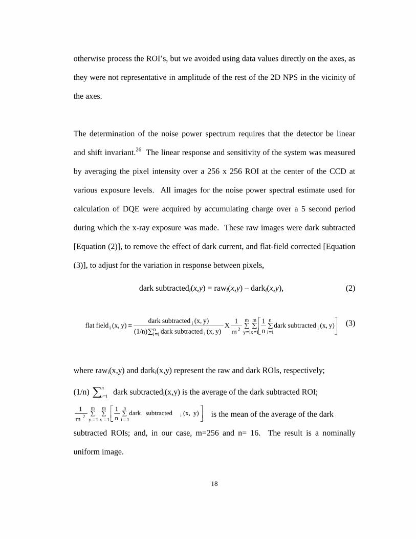
The determination of the noise power spectrum requires that the detector be linear
and shift invariant.26 The linear response and sensitivity of the system was measured
by averaging the pixel intensity over a 256 x 256 ROI at the center of the CCD at
various exposure levels. All images for the noise power spectral estimate used for
calculation of DQE were acquired by accumulating charge over a 5 second period
during which the x-ray exposure was made. These raw images were dark subtracted
[Equation (2)], to remove the effect of dark current, and flat-field corrected [Equation
(3)], to adjust for the variation in response between pixels,
dark subtractedi(x,y) = rawi(x,y) – darki(x,y), (2)
∑ ∑
∑
∑=
= = ==
m
1y
m
1x
n
1ii2n
1i i
ii y)(x,subtracteddark
n1
m1X
y)(x,subtracteddark (1/n)y)(x,subtracteddark
y)(x,fieldflat (3)
where rawi(x,y) and darki(x,y) represent the raw and dark ROIs, respectively;
(1/n) ∑ =
n
i 1dark subtractedi(x,y) is the average of the dark subtracted ROI;
is the mean of the average of the dark
subtracted ROIs; and, in our case, m=256 and n= 16. The result is a nominally
uniform image.

19
The ROIs (256 x 256) used for the NPS analysis were taken from the same location
(centered) from multiple (16) images. Though the detector might not to be
completely shift invariant, the process of flat-field correcting and using the same ROI
from multiple images for NPS analysis allows for the reasonable assumption of the
“shift-invariant” property of the system16.
The noise power spectra were determined at four exposure levels, and with two
different scintillators, and were obtained with 4.5 cm thick Lucite in the x-ray beam
path. This thickness of Lucite was used as it was found to be the median thickness
range (4.5 - 4.99 cm) of the compressed breast from a random sample of 100 patient
exams obtained from a population of 1400 patients16. In order to minimize the
detection of scattered radiation, the 4.5-cm-thick Lucite block was mounted onto the
tube housing. The experimental setup for NPS measurement is shown in Figure 5.
Sixteen dark-image subtracted, flat-field corrected, images were acquired as
described previously. Before performing dark-image subtraction and flat-field
correction, the pixel intensity values were converted to 32 bit floating point numbers,
from the original 16 bit digital values, to avoid truncation error. The ensemble
average of the squares of the magnitude of these 16 Fourier transformed 256 x 256
ROI, scaled as shown in Equation (4), provided the 2D raw noise power spectrum,
NPSraw(u,v).

20
Figure 5. Experimental setup for NPS measurement
The NPSraw(u, v) was obtained by
[ ]
yxyx
raw NN
yxflatfieldFTvuNPS ∆∆=
2),(),( (4)
Support Assembly
X-ray Source
Collimator with 4.5 cm Lucite attenuator
CCD
65 cm
Readout to computer
Scintillator
Light shield (Cover)

21
where [ ] 2),( yxflatfieldFT represents the ensemble average of the squares of the
magnitude of the Fourier transformed 256 x 256 ROI’s, Nx and Ny are the number of
elements in the x and y directions respectively (which are equal and 256 in this case),
and ∆x and ∆y are the pixel pitch in the x and y directions, respectively. The pixel
pitch for the full field image is 24 µm. For the 2 x 2, 3 x 3 and 4 x 4 binned images,
the pixel pitch is 48 µm, 72 µm and 96 µm respectively.
The 2D NPSnormalized(f) to be used for the DQE calculations was obtained by scaling
the 2D NPSraw(f) for the mean signal by
( )2ROI 256 x 256 of signalmean
)()(
fNPSfNPS raw
normalized = (5)
The mean signal of the 256 x 256 ROI is expressed in digital values.
To compute the noise equivalent quanta (NEQ), a commonly used form of the signal
to noise ratio, and the DQE, a 1D NPS curve was required. This was achieved by
using a radial-averaging technique. For each data value (u,v) at radius r from the
center of the image (excluding the axes), the frequency was computed as
22 vu + for the 1D NPS estimate. The final 1D NPS at each exposure level is the
average of 128 data points grouped into frequency bins. Each bin represents 0.164

22
cycles/mm for 24 micron pixels (no binning), 0.082 cycles/mm for 48 micron pixels
(2 x 2 binning), 0.055 cycles/mm for 72 micron pixels (3 x 3 binning) and 0.042
cycles/mm for 96 micron pixels (4 x 4 binning).
D. NEQ and DQE measurement
The NEQ was computed as
)(NPS
)(MTF)(NEQnormalized
2
fff = (6)
The NEQ of the system was computed for the four exposure levels at each binning
configuration. For the purpose of calculating the DQE of the imaging system, Eqs (7)
and (8) were used24:
qf
ff)(NPS
)(MTF)DQE(
normalized
2
= (7)
and hence
q
ff )(NEQ)DQE( = (8)

23
where MTF(f) is the modulation transfer function of the system; NPSnormalized(f) is the
normalized noise power spectrum of the imaging system; q is the number of x-ray
photons incident on the detector per unit area; NEQ(f) is the noise equivalent quanta
of the imaging system and f is the spatial frequency. The only factor that needs to be
determined is q and this has previously been done for this system16.

24
III. RESULTS
A. Presampling MTF
An object can be represented in the frequency domain by a series of discrete
frequencies. The modulation transfer function (MTF) is a measure of the ability of a
system to reproduce the original object frequencies in the final image. Figures 6
through 9 show and compare the MTF curves for this imaging system with a Kodak
MIN-R 2000™ scintillator and with a CsI:Tl scintillator. Figure 6 and Figure 7 show
that the MTF decreases slightly as pixel size increases for both scintillators. Since
larger pixels cannot adequately sample high frequencies this result is expected.
Larger pixels can sample low frequencies as well as small pixels can so the curves
tend to merge at low frequencies. Because small objects or abrupt changes in x-ray
attenuation are represented by high frequencies systems must be capable of detecting
these higher frequencies in order to display small objects. This is especially
important in applications such as mammography where microcalcifications tenths of a
mm in diameter provide early evidence of cancer.

25
0
0.1
0.2
0.3
0.4
0.5
0.6
0.7
0.8
0.9
1
0 2 4 6 8 10 12 14 16 18 20
Spatial Frequency (cycles/mm)
Mod
ulat
ionT
rans
fer F
unct
ion
1x1 (24 micron)
2x2 (48 micron)
3x3 (72 micron)
4x4 (96 micron)
Figure 6. Presampling MTF for Kodak MIN-R 2000™ scintillator for 24 micron (unbinned), 48 micron, 72 micron and 96 micron pixel sizes through hardware binning.

26
Figure 7. Presampling MTF for CsI:Tl scintillator for 24 micron (unbinned), 48 micron, 72 micron and 96 micron pixel sizes through hardware binning.
Figure 8 and Figure 9 compare the MTF curves of Kodak MIN-R 2000™ and CsI:Tl
with and without pixel binning. In Figure 8 the curves show the MTF without
binning, i.e. with a 24 micron pixel. This shows that up to about 3 cycles/mm the two
scintillators are comparable. Above 3 cycles/mm the CsI:Tl MTF is greater than the
Kodak MIN-R 2000™ MTF. In this system, the MTF of Kodak MIN-R 2000™
0
0.1
0.2
0.3
0.4
0.5
0.6
0.7
0.8
0.9
1
0 2 4 6 8 10 12 14 16 18 20
Spatial Frequency (cycles/mm)
Mod
ulat
ion
Tran
sfer
Fun
ctio
n
1x1 (24 micron)
2x2 (48 micron)
3x3 (72 micron)
4x4 (96 micron)

27
drops below 0.1 at about 9.5 cycles/mm while the CsI:Tl MTF remains above 0.1
until about 13.5 cycles/mm. This shows that with the CsI:Tl scintillator this system
is capable reproducing higher frequencies than with the Kodak MIN-R 2000™.
Figure 8. Comparison of MTF with Kodak MIN-R 2000™ and CsI:Tl, with no binning (24 micron). Above 3 cycles/mm the CsI:Tl MTF is greater than the Kodak MIN-R 2000™ MTF and the CsI:Tl MTF is greater than 0.1 up to 13.5 cycles/mm while the Kodak MIN-R 2000™ MTF drops below 0.1 at 9.5 cycles/mm.
0
0.1
0.2
0.3
0.4
0.5
0.6
0.7
0.8
0.9
1
0 1 2 3 4 5 6 7 8 9 10 11 12 13 14 15 16 17 18 19 20 21
Spatial Frequency (cycles/mm)
Mod
ulat
ion
Tran
sfer
Fun
ctio
n
CsI
MINR 2000

28
Figure 9 compares the MTF curves with 4 x 4 hardware binning which produces a 96
micron pixel. In this case the Kodak MIN-R 2000™ curve appears to be slightly
higher than the CsI:Tl curve up to about 3.5 cycles/mm. From that point up to the
Figure 9. Comparison of MTF with Kodak MIN-R 2000™ and CsI:Tl, with 4 x 4 binning (96 micron). Above 3 cycles/mm the CsI:Tl MTF is slightly greater than the Kodak MIN-R 2000™ MTF indicating that there may be a slight improvement in resolution when the CsI:Tl scintillator is used.
0
0.1
0.2
0.3
0.4
0.5
0.6
0.7
0.8
0.9
1
0 1 2 3 4 5 6
Spatial Frequency (cycles/mm)
Mod
ulat
ion
Tran
sfer
Fun
ctio
n CsI
MINR 2000

29
Nyquist limit, CsI:Tl shows a higher MTF. This indicates that there may be a slight
improvement in resolution when the CsI:Tl scintillator is used. This is typical of 2 x
2 and 3 x 3 binning (48 micron and 76 micron pixels, respectively), for which results
are not shown.
B. NPS
Figures 10 through 17 show and compare the 1-D NPS curves for this system.
Figures 10 and 11 show the NPS curves for Kodak MIN-R 2000™ and CsI:Tl
respectively, with no binning, at the four exposure levels used. Both curves show that
the normalized NPS decreases as exposure increases for both scintillators. Figures 12
and 13 compare the NPS curves for Kodak MIN-R 2000™ and CsI:Tl, with no
binning, at exposures of 5 mAs (1.41 mR) and 20 mAs (5.62 mR), respectively. Both
curves show that CsI:Tl has lower noise than Kodak MIN-R 2000™. This is also true
for exposures of 10 mAs (2.82 mR) and 16 mAs (4.50 mR), for which results are not
shown.

30
Figure 10. NPS at 5, 10, 16 and 20 mAs with Kodak MIN-R 2000™ with no binning (24 micron). As expected, the normalized NPS decreases as exposure increases.
0.0E+00
5.0E-06
1.0E-05
1.5E-05
2.0E-05
2.5E-05
3.0E-05
3.5E-05
4.0E-05
4.5E-05
0 2 4 6 8 10 12 14 16
Spatial Frequency (cycles/mm)
NPS
(mm
2 )
5mAs
10mAs
16mAs
20mAs

31
Figure 11. NPS at 5, 10, 16 and 20 mAs with CsI:Tl with no binning (24 micron). As expected, the normalized NPS decreases as exposure increases.
0.0E+00
5.0E-06
1.0E-05
1.5E-05
2.0E-05
0 2 4 6 8 10 12 14 16
Spatial Frequency (cycles/mm)
NPS
(mm
2 )
5mAs
10mAs
16mAs
20mAs

32
Figure 12. NPS comparison of Kodak MIN-R 2000™ and CsI:Tl at 5 mAs with no binning (24 micron). CsI shows lower noise, particularly at low frequencies, than Kodak MIN-R 2000™.
0.0E+00
5.0E-06
1.0E-05
1.5E-05
2.0E-05
2.5E-05
3.0E-05
3.5E-05
4.0E-05
4.5E-05
0 2 4 6 8 10 12 14 16
Spatial Frequency (cycles/mm)
NPS
(mm
2 )
MINR 5mAs
CsI 5mAs

33
Figure 13. NPS comparison of Kodak MIN-R 2000™ and CsI:Tl at 20 mAs with no binning (24 micron). CsI shows lower noise, particularly at low frequencies, than Kodak MIN-R 2000™.
0.0E+00
2.0E-06
4.0E-06
6.0E-06
8.0E-06
1.0E-05
1.2E-05
0 2 4 6 8 10 12 14 16
Spatial Frequency (cycles/mm)
NPS
(mm
2 )
MINR 20mAs
CsI 20mAs

34
There was much less of a difference in the 1-D NPS as a function of pixel size as
shown in Figures 14 and 15. In these figures hardware binning is used. Figure 14
shows the NPS as pixel size increases for Kodak MIN-R 2000™ at 5 mAs, Figure 15
shows the same curves for CsI:Tl. These curves at 20 mAs are shown as Figures A1
and A2 of Appendix A.
Figure 14. NPS for Kodak MIN-R 2000™ at 5 mAs for 24 micron, 48 micron, 72 micron and 96 micron pixel sizes. NPS decreases slightly as pixel size increases reflecting the relative increase in signal. No significant improvement in noise is noted.
0.0E+00
5.0E-06
1.0E-05
1.5E-05
2.0E-05
2.5E-05
3.0E-05
3.5E-05
4.0E-05
4.5E-05
5.0E-05
0 2 4 6 8 10 12 14 16 18 20 22
Spatial Frequency (cycles/mm)
NPS
(mm
2 )
1x1 (24 micron)
2x2 (48 micron)
3x3 (72 micron)
4x4 (96 micron)

35
Figure 15. NPS for CsI:Tl at 5 mAs for 24 micron, 48 micron, 72 micron and 96 micron pixel sizes. As in the case of Kodak MIN-R 2000™, NPS decreases slightly as pixel size increases reflecting the relative increase in signal. No significant improvement in noise is noted.
In all cases, and in the cases of 10 mAs and 16 mAs exposures which are not shown,
NPS decreases slightly as pixel size increases. While this reflects the relative
increase in signal as pixel size increases it does not indicate a significant
improvement in noise as is noted when comparing Kodak MIN-R 2000™ and CsI:Tl.
0.0E+00
5.0E-06
1.0E-05
1.5E-05
2.0E-05
2.5E-05
3.0E-05
3.5E-05
0 2 4 6 8 10 12 14 16 18 20 22
Spatial Frequency (cycles/mm)
NPS
(mm
2 )
1x1 (24 micron)
2x2 (48 micron)
3x3 (72 micron)
4x4 (96 micron)
36
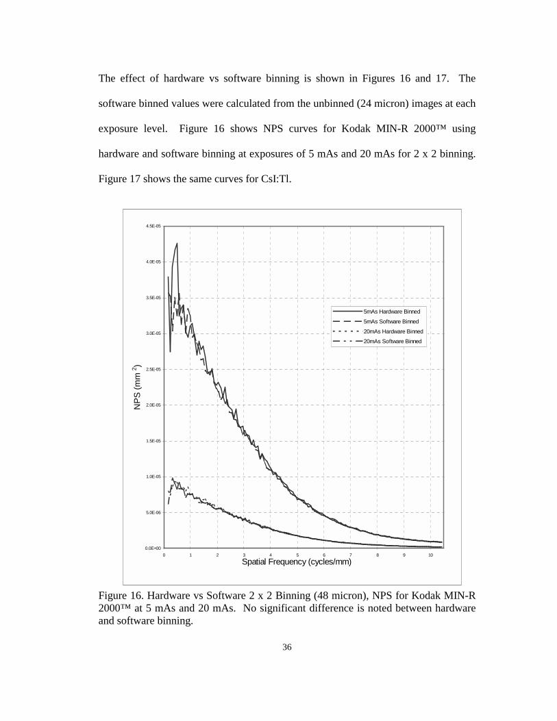
The effect of hardware vs software binning is shown in Figures 16 and 17. The
software binned values were calculated from the unbinned (24 micron) images at each
exposure level. Figure 16 shows NPS curves for Kodak MIN-R 2000™ using
hardware and software binning at exposures of 5 mAs and 20 mAs for 2 x 2 binning.
Figure 17 shows the same curves for CsI:Tl.
Figure 16. Hardware vs Software 2 x 2 Binning (48 micron), NPS for Kodak MIN-R 2000™ at 5 mAs and 20 mAs. No significant difference is noted between hardware and software binning.
0.0E+00
5.0E-06
1.0E-05
1.5E-05
2.0E-05
2.5E-05
3.0E-05
3.5E-05
4.0E-05
4.5E-05
0 1 2 3 4 5 6 7 8 9 10
Spatial Frequency (cycles/mm)
NPS
(mm
2 )
5mAs Hardware Binned
5mAs Software Binned
20mAs Hardware Binned
20mAs Software Binned

37
Figure 17. Hardware vs Software 2 x 2 Binning (48 micron), NPS for CsI:Tl at 5 mAs and 20 mAs. As with Kodak MIN-R 2000™, no significant difference is noted between hardware and software binning. These curves for 3 x 3 binning (72 micron) and 4 x 4 binning (96 micron) are
included in Appendix A as Figures A3 and A4 for Kodak MIN-R 2000™, and A5 and
A6 for CsI:Tl. Not shown are NPS curves for exposures of 10 mAs and 16 mAs,
which follow the trends of the curves shown. In all cases, there is no significant
difference between hardware and software binning.
0.0E+00
5.0E-06
1.0E-05
1.5E-05
2.0E-05
2.5E-05
3.0E-05
0 1 2 3 4 5 6 7 8 9 10
Spatial Frequency (cycles/mm)
NPS
(mm
2 )
5mAs Hardware Binned5mAs Software Binned20mAs Hardware Binned20mAs Software Binned

38
This indicates that the read noise per pixel for this CCD is very low when compared
to the signal per pixel and that where maximum resolution is not needed either
binning technique can be used without degrading image quality.
C. NEQ
The NEQ is shown in Figures 18 through 24 indicating how the signal to noise ratio
changes with exposure and pixel size. Figures 18 and 19 show how the NEQ with no
binning varies at different exposures for Kodak MIN-R 2000™ and CsI:Tl
respectively. As expected in both cases, NEQ is higher at higher exposures. With
hardware binning the results are the same, as shown in Figures 20 and 21, NEQ with
4 x 4 binning (96 micron) at different exposures for Kodak MIN-R 2000™ and CsI:Tl
respectively. This was also true with 2 x 2 binning (48 micron) and 3 x 3 binning (72
micron) for which results are not shown.

39
Figure 18. NEQ for Kodak MIN-R 2000™ with no binning at 5 mAs, 10 mAs, 16 mAs and 20 mAs. As expected, the NEQ increases with exposure.
0
20000
40000
60000
80000
100000
120000
140000
0 2 4 6 8 10 12 14 16 18 20
Spatial Frequency (cycles/mm)
NEQ
(mm
-2)
20 mAs (300170 quanta)
16 mAs (240350 quanta)
10 mAs (150085 quanta)
5 mAs (75310 quanta)

40
Figure 19. NEQ for CsI:Tl with no binning at 5 mAs, 10 mAs, 16 mAs and 20 mAs. As with Kodak MIN-R 2000™, the NEQ increases with exposure.
0
50000
100000
150000
200000
250000
0 2 4 6 8 10 12 14 16 18 20
Spatial Frequency (cycles/mm)
NEQ
(mm
-2)
20 mAs (300170 quanta)
16 mAs (240350 quanta)
10 mAs (150085 quanta)
5 mAs (75310 quanta)

41
Figure 20. NEQ for Kodak MIN-R 2000™ with 4 x 4 binning at 5 mAs, 10 mAs, 16 mAs and 20 mAs. As previously noted, the NEQ increases with exposure.
0
20000
40000
60000
80000
100000
120000
0 1 2 3 4 5 6
Spatial Frequency (cycles/mm)
NEQ
(mm
-2)
20 mAs (300170 quanta)
16 mAs (240350 quanta)
10 mAs (150085 quanta)
5 mAs (75310 quanta)

42
Figure 21. NEQ for CsI:Tl with 4 x 4 binning at 5 mAs, 10 mAs, 16 mAs and 20 mAs. As with Kodak MIN-R 2000™, the NEQ increases with exposure.
Using the highest exposure, 20 mAs (5.62 mR), NEQ shows no significant difference
as pixel size changes. Figures 22 and 23 show the NEQ at 20 mAs, for Kodak MIN-
R 2000™ and CsI:Tl, respectively for each pixel size.
0
50000
100000
150000
200000
250000
0 1 2 3 4 5 6
Spatial Frequency (cycles/mm)
NEQ
(mm
-2)
20 mAs (300170 quanta)
16 mAs (240350 quanta)
10 mAs (150085 quanta)
5 mAs (75310 quanta)

43
Figure 22. NEQ for Kodak MIN-R 2000™ at 20 mAs (300170 quanta) for 24 micron, 48 micron, 72 micron and 96 micron pixels. The NEQ shows no significant difference as pixel size changes.
0
20000
40000
60000
80000
100000
120000
140000
0 2 4 6 8 10 12 14 16 18 20
Spatial Frequency (cycles/mm)
NEQ
(mm
-2)
1x1 (24 micron)
2x2 (48 micron)
3x3 (72 micron)
4x4 (96 micron)

44
Figure 23. NEQ for CsI:Tl at 20 mAs (300170 quanta) for 24 micron, 48 micron, 72 micron and 96 micron pixels. The NEQ shows no significant difference as pixel size changes.
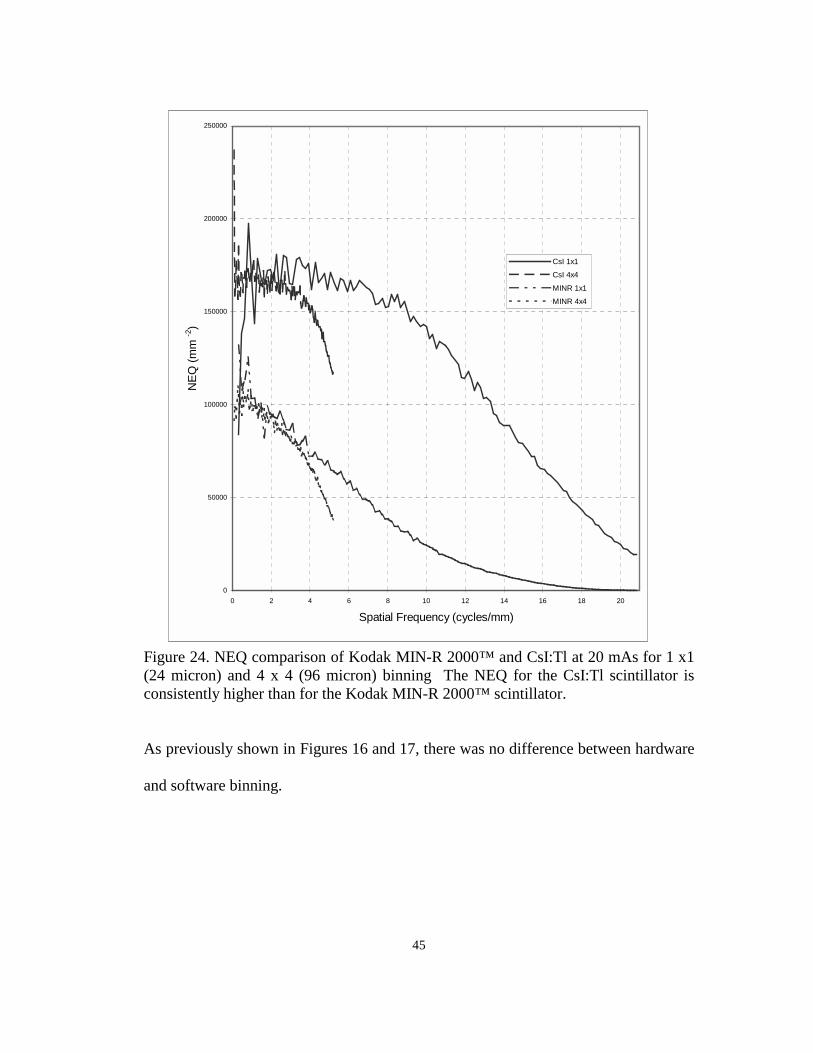
The NEQ for the CsI:Tl scintillator is consistently higher than for the Kodak MIN-R
2000™ scintillator. This is shown in Figure 24, NEQ at 20 mAs using 1 x 1 (24
micron) and 4 x 4 (96 micron) binning with both scintillators. Results followed the
same trend at all exposures.
0
50000
100000
150000
200000
250000
0 2 4 6 8 10 12 14 16 18 20
Spatial Frequency (cycles/mm)
NEQ
(mm
-2)
1x1 (24 micron)
2x2 (48 micron)
3x3 (72 micron)
4x4 (96 micron)
45
Figure 24. NEQ comparison of Kodak MIN-R 2000™ and CsI:Tl at 20 mAs for 1 x1 (24 micron) and 4 x 4 (96 micron) binning The NEQ for the CsI:Tl scintillator is consistently higher than for the Kodak MIN-R 2000™ scintillator.
As previously shown in Figures 16 and 17, there was no difference between hardware
and software binning.
0
50000
100000
150000
200000
250000
0 2 4 6 8 10 12 14 16 18 20
Spatial Frequency (cycles/mm)
NEQ
(mm
-2)
CsI 1x1
CsI 4x4
MINR 1x1
MINR 4x4

46
D. DQE
The photon flux incident on the detector was previously determined to be 5.34 x10⁴
photons/mm2/mR. The exposure at the detector was determined by measuring the
exposure at a distance of 45 cm and calculating the exposure at 65 cm. These were
then used to calculate the DQE.
The DQE of the system at the four exposure levels without binning is shown in
Figure 25 for Kodak MIN-R 2000™ and in Figure 26 for CsI:Tl. As shown, there is
minimal influence by exposure on the DQE for either scintillator. DQE is influenced
by scintillator, however, as shown in Figure 27, DQE without binning at 5 mAs and
20 mAs for both scintillators. This continues to hold true with hardware binning as
shown in Appendix A, Figures A7, A8 and A9, DQE at 5 mAs and 20 mAs for both
scintillators with 2 x 2 (48 micron), 3 x 3 (72 micron) and 4 x 4 (96 micron) binning,
respectively.
As previously noted in Figures 16 and 17, the binning method does not change the
results. Comparisons of hardware and software binning are shown in Appendix A,
Figures A10, A11 and A12, which depict the DQE for hardware and software binning
at 5 mAs for both scintillators at 2 x 2 (48 micron), 3 x 3 (72 micron) and 4 x 4 (96
micron) binning, respectively.

47
Figure 25. DQE for Kodak MIN-R 2000™ without binning at exposures of 5 mAs, 10 mAs, 16 mAs and 20 mAs. There is minimal influence of exposure on DQE.
0
0.05
0.1
0.15
0.2
0.25
0.3
0.35
0.4
0.45
0 2 4 6 8 10 12 14 16 18 20
Spatial Frequency (cycles/mm)
DQ
E
5 mAs
10 mAs
16 mAs
20 mAs

48
Figure 26. DQE for CsI:Tl without binning at 5 mAs, 10 mAs, 16 mAs and 20 mAs. As with Kodak MIN-R 2000™, there is minimal influence of exposure on DQE..
0
0.1
0.2
0.3
0.4
0.5
0.6
0.7
0 2 4 6 8 10 12 14 16 18 20
Spatial Frequency (cycles/mm)
DQ
E5 mAs
10 mAs
16 mAs
20 mAs

49
Figure 27. DQE comparison of Kodak MIN-R 2000™ and CsI:Tl without binning at exposures of 5 mAs and 20 mAs. Not only is the DQE of the CsI:Tl initially higher than that of the Kodak MIN-R 2000™, it remains relatively high and does not begin to drop off until it reaches 10 cycles/mm. While the DQE for the Kodak MIN-R 2000™ falls below 0.1 at 9.5 cycles/mm, the DQE for the CsI:Tl does not drop below 0.1 until 19 cycles/mm.
0
0.1
0.2
0.3
0.4
0.5
0.6
0.7
0.8
0 2 4 6 8 10 12 14 16 18 20
Spatial Frequency (cycles/mm)
DQ
E
CsI 5 mAs
CsI 20 mAs
MINR 5 mAs
MINR 20 mAs

50
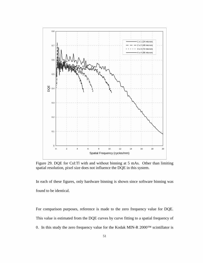
There is also minimal influence by pixel size on the DQE as shown in Figures 28 and
29, DQE at 5 mAs with and without binning for Kodak MIN-R 2000™ and CsI:Tl
respectively. This holds true as exposure increases as shown in Appendix A, Figures
A13 and A14, 10 mAs; A15 and A16, 16 mAs and A17 and A18, 20 mAs.
Figure 28. DQE for Kodak MIN-R 2000™ with and without binning at 5 mAs. Other than limiting spatial resolution, pixel size does not influence the DQE in this system.
0
0.05
0.1
0.15
0.2
0.25
0.3
0.35
0.4
0.45
0.5
0 2 4 6 8 10 12 14 16 18 20
Spatial Frequency (cycles/mm)
DQ
E
1 x 1 (24 micron)
2 x 2 (48 micron)
3 x 3 (72 micron)
4 x 4 (96 micron)
51
Figure 29. DQE for CsI:Tl with and without binning at 5 mAs. Other than limiting spatial resolution, pixel size does not influence the DQE in this system.
In each of these figures, only hardware binning is shown since software binning was
found to be identical.
For comparison purposes, reference is made to the zero frequency value for DQE.
This value is estimated from the DQE curves by curve fitting to a spatial frequency of
0. In this study the zero frequency value for the Kodak MIN-R 2000™ scintillator is
0
0.1
0.2
0.3
0.4
0.5
0.6
0.7
0.8
0 2 4 6 8 10 12 14 16 18 20
Spatial Frequency (cycles/mm)
DQ
E
1 x 1 (24 micron)
2 x 2 (48 micron)
3 x 3 (72 micron)
4 x 4 (96 micron)

52
approximately 0.35. The zero frequency value for the CsI:Tl scintillator is
approximately 0.6. For a clinical prototype, full breast digital mammography system
the zero frequency DQE at comparable exposures was approximately 0.4816.

53
IV. DISCUSSION
As shown in Figure 8, the resolution characteristics of the CsI:Tl scintillator are
comparable to the Kodak MIN-R 2000™ scintillator at low frequencies, but exhibits a
higher MTF above about 3 cycles/mm. This indicates that the CsI:Tl scintillator has a
greater ability to reproduce the higher frequencies that represent smaller objects and
sharper edges. This is particularly important in applications such as mammography
where small microcalcifications and the shape of masses provide early evidence of
cancer.
The data also shows that there is a small increase in the MTF as the pixel size
decreases. This difference is expected since larger pixels cannot adequately sample
higher frequencies.
As shown in Figures 12 and 13, the normalized NPS for the Kodak MIN-R 2000™
scintillator is higher than that for the CsI:Tl scintillator. This is noted particularly at
low frequencies and may be due to the columnar structure of the CsI:Tl scintillator.
This is also reflected in the NEQ and DQE results showing that the CsI:Tl scintillator
produced not only higher NEQ and DQE but maintained those high levels to a higher
frequency than the Kodak MIN-R 2000™ scintillator. Figure 30 shows the NEQ
comparison and Figure 33 shows the DQE comparison. In both cases the Kodak
MIN-R 2000™ scintillator curve falls off sharply as frequency increases while the

54
CsI:Tl scintillator curve stays very close to the zero frequency value almost halfway
to the limiting frequency.
The NEQ results showed an increase with increased exposure, as expected since
increased exposure provides increased signal. The results also showed no significant
difference as pixel size decreased. This indicates that noise in the system was
dominated by the x-ray photon (quantum) noise.
The results showed no significant difference in DQE with either exposure or pixel
size. This also indicates that the noise in the system is predominantly x-ray photon
noise. It also indicates that exposure need not be increased to improve image quality
and that decreasing pixel size does not necessarily degrade image quality.

55
V. CONCLUSION
By using a very low-noise CCD the DQE of a digital x-ray imaging system can be
maintained while pixel size is reduced. Combined with a properly designed
scintillator resolution can be substantially improved without compromising image
quality.
Where maximum resolution is not required, hardware or software binning can be used
to increase pixel size. Hardware and software binning were shown to be identical
with no degradation of image quality.
While gadolinium oxysulfide screens, such as Kodak MIN-R 2000™, are well suited
for use with film, they do not perform as well as a scintillator designed for use with a
CCD. For the system represented in Figure 28, the DQE falls to 0.1 at about 9
cycles/mm for both the 48 micron pixel (2 x 2 binning) and the 24 micron pixel (no
binning). Using 0.1 as a lower limit for DQE, and maintaining the exposure at 5
mAs, this system with a 48 micron pixel will perform as well as this system with a 24
micron pixel, i.e. smaller objects and sharper edges will not be imaged any more
clearly with this system with a 24 micron pixel.
The columnar structure of CsI:Tl appears to be far superior to the granular structure
of gadolinium oxysulfide. The DQE using the CsI:Tl scintillator achieved a higher
initial DQE and maintained a relatively high DQE to a higher frequency than did the

56
DQE using Kodak MIN-R 2000™. For the system represented in Figure 29 the DQE,
at an exposure of 5 mAs, for the 96 micron pixel (4 x 4 binning), the 72 micron pixel
(3 x 3 binning) and the 48 micron pixel (2 x 2 binning) is greater than 0.35 when the
Nyquist limits are reached. For the 24 micron pixel (no binning) the DQE falls to 0.1
at about 19 cycles/mm. In this system, at an exposure of 5 mAs, resolution will be
increased by reducing the pixel size to 24 microns. Compared with the above Kodak
MIN-R 2000™ scintillator, this system will have more than twice the resolution and
would have slightly better resolution than current screen-film mammography systems
that operate in the 16 to 18 cycles/mm range.

57
REFERENCES
1. Bunch P, The effects of reduced film granularity on mammographic image
quality. Opt. Soc. Int. Eng. (SPIE), 3032, 302-317 (1997). 2. Yoshida H, Doi K, Nishikawa RM, et al: An improved computer-assisted
diagnostic scheme using wavelet transform for detecting clustered microcalcifications in digital mammograms. Acad Radiol 3(8): 621-627, 1996.
3. Anastasio MA, Yoshida H, Nagel R, et al: A genetic algorithm-based method for
optimizing the performance of a computer-aided diagnosis scheme for detection of clustered microcalcifications in mammograms. Med Phys 25(9): 1613-1620, 1998.
4. Suryanarayanan S, Karellas A, Vedantham S, et al: Comparison of Tomosynthesis
Methods Used with Digital Mammography. Acad Radiol 2000; 7:1085-1097 (2000).
5. Chakraborty DP and Barnes GT, An energy sensitive cassette for dual-energy
mammography, Med. Phys. 16(1), 7-13 (1989). 6. Flanagan FL, Murray JG, Gilligan P, Stack JP and Ennis JT, Digital subtraction in
Gd-DTPA enhanced imaging of the breast, Clin. Radiol. 50(12), 848-854 (1995). 7. Hillen W, Schiebel U, and Zaengel T, Imaging performance of a storage phosphor
system, Med. Phys. 14(5), 744-751 (1987). 8. Hillen W, Schiebel U, and Zaengel T: A selenium-based detector system for
digital slot-radiography. SPIE Vol. 914 Medical Imaging II 253-261, 1988 9. Neitzel U, Maack I, Gunther-Kohfahl S: Image quality of a digital chest
radiography system based on a selenium detector. Med Phys 21(4): 509-516, 1994.
10. Zhao W, Rowlands JA: Digital radiology using active matrix readout of
amorphous selenium: Construction and evaluation of a prototype real-time detector. Med Phys 24(12): 1834-1843, 1997.
11. Antonuk LE, El-Mohri Y, Jee K, et al: Performance Evaluation of a Large Area,
97 µm Pitch: Indirect Detection Active Matrix Flat-panel Imager (AMFPI) for Radiography and Fluoroscopy. Radiology 209(P): 357, 1998.

58
12. Siewerdsen JH, Antonuk LE, El-Mohri Y, et al: Empirical and theoretical
investigation of the noise performance of indirect detection, active matrix flat-panel imagers (AMFPIs) for diagnostic radiology. Med Phys 24(1): 71-89, 1997.
13. Hejazi S, Trauernicht DP: System considerations in CCD-based x-ray imaging for
digital chest radiography and digital mammography. Med Phys 24(2): 287-297, 1997.
14. Karellas, L.J. Harris, H. Liu, M.A. Davis and C.J. D’Orsi, “Charge-coupled
device detector: Performance considerations and potential for small-field mammographic imaging applications,” Med. Phys. 19(4), 1015-1023 (1992).
15. Bradford CD, Peppler WW and Dobbins JT, Performance characteristics of a
Kodak computed radiography system, Med. Phys. 26(1), 27-37 (1999). 16. Vedantham S, Karellas A, Suryanarayanan S, et al: Full Breast Digital
Mammographic Imaging with an Amorphous Silicon-based Flat Panel Detector: Physical Characteristics of a Clinical Prototype. Med Phys 27(3): 558-567, 2000.
17. Vedantham S, Karellas A, Suryanarayanan S, et al: Breast Imaging Using an
Amorphous Silicon-based Full-Field Digital Mammogaphic System: Stability of a Clinical Prototype. Journal of Digital Imaging, Vol 13, No 4, 191-199, 2000.
18. Vedantham S, Karellas A, Suryanarayanan S, et al: Mammographic Imaging with
a small format CCD-based digital cassette: Physical characteristics of a clinical system. Med Phys 27(8), 2000.
19. MacMahon H, Vyborny C, Powell G, et al: The effect of pixel size on the
detection rate of early pulmonary sarcoidosis in digital chest radiographic systems. Medical Imaging and Instrumentaion 14-20, 1984
20. Freedman M, Steller D, et al: Digital Mammography: Tradeoffs between 50 and
100 micron pixel size. Proc. Of SPIE Vol 2432, Medical Imaging 1995 21. Chan H-P, Helvie MA, Petrick N, et al: Digital Mammography: Observer
Performance Study of the Effects of Pixel Size on Radiologists’ Characterization of Malignant and Benign Microcalcifications. Proc. Of SPIE Vol 3659, Medical Imaging 1999
22. Lewin J M, Hendrick R E, D’Orsi CJ, et al: Comparison of Full-Field Digital
Mammography with Screen-Film Mammography for Cancer Detection: Results of 4,945 Paired Examinations. Radiology 2001; 218:873-880

59
23. Fujita H, Tsai DY, Itoh T, Doi K, Morishita J, Ueda K, and Ohtsuka A, A simple
method for determining the modulation transfer function in digital radiography, IEEE Trans. Med. Imaging 11, 34-39 (1992)
24. Dobbins JT, Ergun DL, Rutz L, Hinshaw DA, Blume H, and Clark DC, DQE(f) of
four generations of computed radiography acquisition devices, Med. Phys. 22, 1581-1593 (1995)
25. Dobbins JT, Effects of undersampling on the proper interpretation of modulation
transfer function, noise power spectra, and noise equivalent quanta of digital imaging systems, Med. Phys. 22, 171-181 (1995)
26. Dainty JC and Shaw R, Image Science (Academic, New York, 1974)

60
Appendix A – Supplemental Figures
Figure A1. NPS for Kodak MIN-R 2000™ at 20 mAs for 24 micron, 48 micron, 72 micron and 96 micron pixel sizes. NPS decreases slightly as pixel size increases even at higher exposures. This reflects the relative increase in signal as pixel size increases while there is no significant improvement in noise.
0.0E+00
2.0E-06
4.0E-06
6.0E-06
8.0E-06
1.0E-05
1.2E-05
0 1 2 3 4 5 6 7 8 9 10 11 12 13 14 15 16 17 18 19 20 21
Spatial Frequency (cycles/mm)
NPS
(mm
2 )
1x1 (24 micron)
2x2 (48 micron)
3x3 (72 micron)
4x4 (96 micron)

61
Figure A2. NPS for CsI:Tl at 20 mAs for 24 micron, 48 micron, 72 micron and 96 micron pixel sizes. As in the case of Kodak MIN-R 2000™, NPS decreases slightly as pixel size increases even at higher exposures. This reflects the relative increase in signal as pixel size increases while there is no significant improvement in noise.
0.0E+00
1.0E-06
2.0E-06
3.0E-06
4.0E-06
5.0E-06
6.0E-06
7.0E-06
8.0E-06
9.0E-06
1.0E-05
0 1 2 3 4 5 6 7 8 9 10 11 12 13 14 15 16 17 18 19 20 21
Spatial Frequency (cycles/mm)
NPS
(mm
2 )
1x1 (24 micron)
2x2 (48 micron)
3x3 (72 micron)
4x4 (96 micron)

62
Figure A3. Hardware vs Software 3 x 3 Binning (72 micron), NPS for Kodak MIN-R 2000™ at 5 mAs and 20 mAs. No significant difference is noted between hardware and software binning.
0.0E+00
5.0E-06
1.0E-05
1.5E-05
2.0E-05
2.5E-05
3.0E-05
3.5E-05
4.0E-05
0 1 2 3 4 5 6 7
Spatial Frequency (cycles/mm)
NPS
(mm
2 )
5mAs Hardware Binned
M5mAs Software Binned
20mAs Hardware Binned
20mAs Software Binned

63
Figure A4. Hardware vs Software 4 x 4 Binning (96 micron), NPS for Kodak MIN-R 2000™ at 5 mAs and 20 mAs. No significant difference is noted between hardware and software binning.
0.0E+00
5.0E-06
1.0E-05
1.5E-05
2.0E-05
2.5E-05
3.0E-05
3.5E-05
4.0E-05
0 1 2 3 4 5 6
Spatial Frequency (cycles/mm)
NPS
(mm
2 )
5mAs Hardware Binned
5mAs Software Binned
20mAs Hardware Binned
20mAs Software Binned

64
Figure A5. Hardware vs Software 3 x 3 Binning (72 micron), NPS for CsI:Tl at 5 mAs and 20 mAs. As with Kodak MIN-R 2000™, no significant difference is noted between hardware and software binning.
0.0E+00
5.0E-06
1.0E-05
1.5E-05
2.0E-05
2.5E-05
3.0E-05
0 1 2 3 4 5 6 7
Spatial Frequency (cycles/mm)
NPS
(mm
2 )
5mAs Hardware Binned
5mAs Software Binned
20mAs Hardware Binned
20mAs Software Binned
65
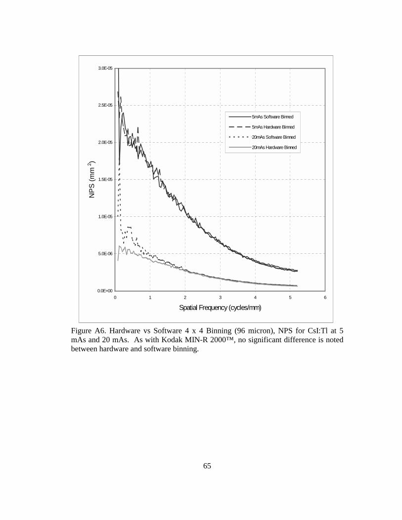
Figure A6. Hardware vs Software 4 x 4 Binning (96 micron), NPS for CsI:Tl at 5 mAs and 20 mAs. As with Kodak MIN-R 2000™, no significant difference is noted between hardware and software binning.
0.0E+00
5.0E-06
1.0E-05
1.5E-05
2.0E-05
2.5E-05
3.0E-05
0 1 2 3 4 5 6
Spatial Frequency (cycles/mm)
NPS
(mm
2 )
5mAs Software Binned
5mAs Hardware Binned
20mAs Software Binned
20mAs Hardware Binned

66
Figure A7. DQE comparison for Kodak MIN-R 2000™ and CsI:Tl with 2 x 2 binning (48 micron) at 5 mAs and 20 mAs. Not only is the DQE of the CsI:Tl initially higher than that of the Kodak MIN-R 2000™, it remains relatively high out to the Nyquist limit. The DQE for the Kodak MIN-R 2000™ falls below 0.1 at 8.5 cycles/mm, while the DQE for the CsI:Tl reaches the Nyquist limit before approaching 0.1.
0
0.1
0.2
0.3
0.4
0.5
0.6
0.7
0.8
0 1 2 3 4 5 6 7 8 9 10 11
Spatial Frequency (cycles/mm)
DQ
ECsI 5 mAs
CsI 20 mAs
MINR 5 mAs
MINR 20 mAs

67
Figure A8. DQE comparison of Kodak MIN-R 2000™ and CsI:Tl with 3 x 3 binning at 5 mAs and 20 mas. Not only is the DQE of the CsI:Tl initially higher than that of the Kodak MIN-R 2000™, it remains relatively high out to the Nyquist limit. The DQE for the Kodak MIN-R 2000™ falls below 0.1 at 6.5 cycles/mm, while the DQE for the CsI:Tl reaches the Nyquist limit before approaching 0.1.
0
0.1
0.2
0.3
0.4
0.5
0.6
0.7
0.8
0 1 2 3 4 5 6 7
Spatial Frequency (cycles/mm)
DQ
E
CsI 20 mAs
CsI 5 mAs
MINR 20 mAs
MINR 5 mAs

68
Figure A9. DQE comparison of Kodak MIN-R 2000™ and CsI:Tl with 4 x 4 binning at 5 mAs and 20 mAs. Not only is the DQE of the CsI:Tl initially higher than that of the Kodak MIN-R 2000™, it remains relatively high out to the Nyquist limit. The DQE for the Kodak MIN-R 2000™ approaches 0.1 at the Nyquist limit (5 cycles/mm), while the DQE for the CsI:Tl reaches the Nyquist limit before approaching 0.1.
0
0.1
0.2
0.3
0.4
0.5
0.6
0.7
0.8
0 0.5 1 1.5 2 2.5 3 3.5 4 4.5 5 5.5
Spatial Frequency (cycles/mm)
DQ
ECsI 20 mAs
CsI 5 mAs
MINR 20 mAs
MINR 5 mAs

69
Figure A10. DQE comparison Kodak MIN-R 2000™ and CsI:Tl with 2 x 2 hardware and software binning at 5 mAs. No significant difference is noted between hardware and software binning.
0
0.1
0.2
0.3
0.4
0.5
0.6
0.7
0 1 2 3 4 5 6 7 8 9 10 11
Spatial Frequency (cycles/mm)
DQ
E
CsI Hardware B inned
CsI So ftware B inned
M INR Hardware B inned
M INRSoftware B inned

70
Figure A11. DQE comparison Kodak MIN-R 2000™ and CsI:Tl with 3 x 3 hardware and software binning at 5 mAs. No significant difference is noted between hardware and software binning.
0
0.1
0.2
0.3
0.4
0.5
0.6
0.7
0 1 2 3 4 5 6 7
Spatial Frequency (cycles/mm)
DQ
E
CsI Hardware Binned
CsI Software Binned
MINR Hardware Binned
MINR Software Binned

71
Figure A12. DQE comparison Kodak MIN-R 2000™ and CsI:Tl with 4 x 4 hardware and software binning at 5 mAs. No significant difference is noted between hardware and software binning.
0
0.1
0.2
0.3
0.4
0.5
0.6
0.7
0.8
0 0.5 1 1.5 2 2.5 3 3.5 4 4.5 5 5.5
Spatial Frequency (cycles/mm)
DQ
E
CsI Hardware Binned
CsI Software Binned
MINR Hardware Binned
MINR Software Binned

72
Figure A13. DQE for Kodak MIN-R 2000™ with and without binning at 10 mAs. Other than limiting spatial resolution, pixel size does not influence the DQE in this system.
0
0.05
0.1
0.15
0.2
0.25
0.3
0.35
0.4
0.45
0.5
0 2 4 6 8 10 12 14 16 18 20
Spatial Frequency (cycles/mm)
DQ
E
1 x 1 (24 micron)
2 x 2 (48 micron)
3 x 3 (72 micron)
4 x 4 (96 micron)

73
Figure A14. DQE for CsI:Tl with and without binning at 10 mAs. Other than limiting spatial resolution, pixel size does not influence the DQE in this system.
0
0.1
0.2
0.3
0.4
0.5
0.6
0.7
0.8
0 2 4 6 8 10 12 14 16 18 20
Spatial Frequency (cycles/mm)
DQ
E
1 x 1 (24 micron)
2 x 2 (48 micron)
3 x 3 (72 micron)
4 x 4 (96 micron)

74
Figure A15. DQE for Kodak MIN-R 2000™ with and without binning at 16 mAs. Other than limiting spatial resolution, pixel size does not influence the DQE in this system.
0
0.05
0.1
0.15
0.2
0.25
0.3
0.35
0.4
0.45
0 2 4 6 8 10 12 14 16 18 20
Spatial Frequency (cycles/mm)
DQ
E
1 x 1 (24 micron)
2 x 2 (48 micron)
3 x 3 (72 micron)
4 x 4 96 micron)

75
Figure A16. DQE for CsI:Tl with and without binning at 16 mAs. Other than limiting spatial resolution, pixel size does not influence the DQE in this system.
0
0.1
0.2
0.3
0.4
0.5
0.6
0.7
0.8
0 2 4 6 8 10 12 14 16 18 20
Spatial Frequency (cycles/mm)
DQ
E
1 x 1 (24 micron)
2 x 2 (48 micron)
3 x 3 72 micron)
4 x 4 (96 micron)

76
Figure A17. DQE for Kodak MIN-R 2000™ with and without binning at 20 mAs. Other than limiting spatial resolution, pixel size does not influence the DQE in this system.
0
0.05
0.1
0.15
0.2
0.25
0.3
0.35
0.4
0.45
0.5
0 2 4 6 8 10 12 14 16 18 20
Spatial Frequency (cycles/mm)
DQ
E
1 x 1 (24 micron)
2 x 2 (48 micron)
3 x 3 (72 micron)
4 x 4 (96 micron)

77
Figure A18. DQE for CsI:Tl with and without binning at 20 mAs. Other than limiting spatial resolution, pixel size does not influence the DQE in this system.
0
0.1
0.2
0.3
0.4
0.5
0.6
0.7
0 2 4 6 8 10 12 14 16 18 20
Spatial Frequency (cycles/mm)
DQ
E1 x 1 (24 micron)
2 x 2 (48 micron)
3 x 3 (72 micron)
4 x 4 (96 micron)