eetop.cn_power integrity for io interfaces.pdf
TRANSCRIPT

8/10/2019 eetop.cn_Power Integrity for IO Interfaces.pdf
http://slidepdf.com/reader/full/eetopcnpower-integrity-for-io-interfacespdf 1/439

8/10/2019 eetop.cn_Power Integrity for IO Interfaces.pdf
http://slidepdf.com/reader/full/eetopcnpower-integrity-for-io-interfacespdf 2/439

8/10/2019 eetop.cn_Power Integrity for IO Interfaces.pdf
http://slidepdf.com/reader/full/eetopcnpower-integrity-for-io-interfacespdf 3/439
Power Integrity for I/O Interfaces: With SignalIntegrity/Power Integrity Co-Design
By: Vishram S. Pandit; Woong Hwan Ryu; Myoung Joon Choi
Publisher: Prentice Hall
Pub. Date: October 13, 2010
Print ISBN-10: 0-13-701119-9
Print ISBN-13: 978-0-13-701119-3
Web ISBN-10: 0-13-259694-6
Web ISBN-13: 978-0-13-259694-7
Pages in Print Edition: 416
Amazon.com® Rating: [0 Ratings]
Subscriber Rating: [0 Ratings]
Overview Table of
Contents
Search This
Book
Hel
Table of Contents
Copyright
Foreword
Preface
Acknowledgments
About the Authors
Chapter 1. Introduction
Section 1.1. Digital Electronic System
Section 1.2. I/O Signaling Standards
Section 1.3. Power and Signal Distribution Network
Section 1.4. Signal and Power Integrity
Section 1.5. Power Noise to Signal Coupling
Section 1.6. Concurrent Design Methodology
References
Chapter 2. I/O Interfaces
Section 2.1. Single-Ended Drivers and Receivers
Section 2.2. Differential Drivers and Receivers
Section 2.3. Prior Stages of I/O Interface
References
Chapter 3. Electromagnetic Effects
Section 3.1. Electromagnetic Effects on Signal/Power Integrity
Section 3.2. Electromagnetic Theory
Section 3.3. Transmission Line Theory

8/10/2019 eetop.cn_Power Integrity for IO Interfaces.pdf
http://slidepdf.com/reader/full/eetopcnpower-integrity-for-io-interfacespdf 4/439
Section 3.4. Interconnection Network Parameters: Z,Y,S and ABCD
Section 3.5. LTI System
References
Chapter 4. System Interconnects
Section 4.1. PCB Technology
Section 4.2. Package Types
Section 4.3. Power Distribution Network
Section 4.4. Signal Distribution Network
Section 4.5. Interaction Between Interconnect Systems
Section 4.6. Modeling Tools for the PDN and Signal Networks
References
Chapter 5. Frequency Domain Analysis
Section 5.1. Signal Spectrum
Section 5.2. Signal and Power Integrity Applications
Section 5.3. Power Distribution Network Design in Frequency Domain
Section 5.4. Signal Network Design in Frequency Domain
References
Chapter 6. Time Domain Analysis
Section 6.1. Time Domain Modeling and Simulation
Section 6.2. Simulation for Optimization
Section 6.3. PDN Noise Simulations
Section 6.4. Jitter Impact for Time Domain Analysis
References
Chapter 7. Signal/Power Integrity Interactions
Section 7.1. Background
Section 7.2. Root Cause Analysis
Section 7.3. SSO Coupling Mechanism
Section 7.4. Case Study I: DDR2 800 Control Signal
Section 7.5. Case Study II: DDR2 667 Vref Bus
Section 7.6. Referencing/Stitching/Decoupling Effects–Single-Ended Interface
Section 7.7. Stitching Effects—Differential Interface [9]
Section 7.8. EMI Trade-Off
References
Chapter 8. Signal/Power Integrity Co-Analysis
Section 8.1. Identifying Controllable Parameters
Section 8.2. SI-PI Modeling and Simulation
Section 8.3. SI-PI Co-Analysis
Section 8.4. SI-PI Co-Simulation and Co-Analysis Flow: Summary

8/10/2019 eetop.cn_Power Integrity for IO Interfaces.pdf
http://slidepdf.com/reader/full/eetopcnpower-integrity-for-io-interfacespdf 5/439
References
Chapter 9. Measurement Techniques
Section 9.1. Frequency Domain Characterization
Section 9.2. Equivalent Circuit Model Extraction
Section 9.3. Time Domain Characterization
References
Index

8/10/2019 eetop.cn_Power Integrity for IO Interfaces.pdf
http://slidepdf.com/reader/full/eetopcnpower-integrity-for-io-interfacespdf 6/439
No part of any chapter or book may be reproduced or transmitted in any form by any means withoutthe prior written permission for reprints and excerpts from the publisher of the book or chapter.Redistribution or other use that violates the fair use privilege under U.S. copyright laws (see 17USC107) or that otherwise violates these Terms of Service is strictly prohibited. Violators will be
prosecuted to the full extent of U.S. Federal and Massachusetts laws.
Copyright
Many of the designations used by manufacturers and sellers to distinguishtheir products are claimed as trademarks. Where those designations appearin this book, and the publisher was aware of a trademark claim, the
designations have been printed with initial capital letters or in all capitals.
The authors and publisher have taken care in the preparation of this book,but make no expressed or implied warranty of any kind and assume noresponsibility for errors or omissions. No liability is assumed for incidentalor consequential damages in connection with or arising out of the use of theinformation or programs contained herein.
The publisher offers excellent discounts on this book when ordered in
quantity for bulk purchases or special sales, which may include electronic
versions and/or custom covers and content particular to your business,training goals, marketing focus, and branding interests. For moreinformation, please contact:
U.S. Corporate and Government Sales(800) [email protected]
For sales outside the United States, please contact:
International [email protected]
Visit us on the Web: informit.com/ph
Library of Congress Cataloging-in-Publication Data:
Pandit, Vishram S. (Vishram Shriram)Power integrity for I/O interfaces : with signal integrity/power integrity co-
design /
Vishram S. Pandit, Woong Hwan Ryu, Myoung Joon Choi.p. cm.
Includes bibliographical references.

8/10/2019 eetop.cn_Power Integrity for IO Interfaces.pdf
http://slidepdf.com/reader/full/eetopcnpower-integrity-for-io-interfacespdf 7/439
ISBN 978-0-13-701119-3 (hardback : alk. paper) 1. Interface circuits—Design andconstruction. 2. Computer interfaces—
Power supply. 3. Signal integrity (Electronics)4. Power electronics. I. Ryu, Woong Hwan, 1971- II. Choi, Myoung Joon, 1973- III. Title.
TK7868.I58P36 2011621.3815--dc22
2010030786
Copyright © 2011 Pearson Education, Inc.
All rights reserved. Printed in the United States of America. This publicationis protected by copyright, and permission must be obtained from thepublisher prior to any prohibited reproduction, storage in a retrieval system,or transmission in any form or by any means, electronic, mechanical,photocopying, recording, or likewise. For information regarding permissions,write to:
Pearson Education, IncRights and Contracts Department501 Boylston Street, Suite 900Boston, MA 02116Fax (617) 671 3447
ISBN-13: 978-0-137-01119-3
Text printed in the United States on recycled paper at Courier in Westford,Massachusetts.
First printing October 2010
Editor-in-Chief Mark Taub
Acquisitions Editor Bernard Goodwin
Managing Editor Kristy Hart
Project Editor Lori Lyons
Copy Editor
Apostrophe Editing Services
Senior Indexer

8/10/2019 eetop.cn_Power Integrity for IO Interfaces.pdf
http://slidepdf.com/reader/full/eetopcnpower-integrity-for-io-interfacespdf 8/439
Cheryl Lenser
Proofreader
Sheri Cain
Technical Reviewers Jory McKinleyEric BogatinSteve Weir
Moises Cases
Publishing Coordinator Michelle Housley
Cover Designer
Anne Jones
Compositor Robert Mauhar
Graphics Laura Robbins
Dedication
We would like to dedicate this book to our families for theirdevotion, untiring support, and encouragement.
—Authors
Vishram S. Pandit thanks his wife, kids, parents, brother and
family.
Woong Hwan Ryu thanks his wife Cindy; his kids Josh, Erin,Lauren, and Jacob; his parents, brothers, sisters, and family.
Myoung Joon Choi thanks his wife Joo Young and his daughterGiana, his parents, his brother and family.

8/10/2019 eetop.cn_Power Integrity for IO Interfaces.pdf
http://slidepdf.com/reader/full/eetopcnpower-integrity-for-io-interfacespdf 9/439
No part of any chapter or book may be reproduced or transmitted in any form by any means withoutthe prior written permission for reprints and excerpts from the publisher of the book or chapter.Redistribution or other use that violates the fair use privilege under U.S. copyright laws (see 17USC107) or that otherwise violates these Terms of Service is strictly prohibited. Violators will be
prosecuted to the full extent of U.S. Federal and Massachusetts laws.
Foreword
With recent advancement of the semiconductor technology, microprocessorsand System-On-Chip (SoC) products are taking advantage of cheaperproduction cost and the extended Moore’s law. This has reinvigorated more
widespread use of personal computing devices and consumer electronicsdevices. Most of these recent electronics systems are getting faster,smaller, and, are operating at lower power. In addition, the design cycle forproducts is getting shorter, putting more pressure on efficient designcapability while the robust operation of devices is a definite requirement.The issues arising from these trends range from physical design,electromagnetic compatibility, electromagnetic interference, to thermal andpower consumption reduction. The designers of the cutting-edge productstry to manage all of these problems together while keeping the overall pricedown as much as possible. Too much over-design tends to make the system
lose competitive edge, and under-design apparently makes the system loseits robustness.
Digital design portion of the semiconductor circuit design has advancedsignificantly since the advent of the transistor CAD design tools. However,
for high-speed Input/Output (IO) interfaces, the digital signals pass throughpower and signal distribution networks, and analog effects becomeimportant. The advances in the analog signaling techniques—or morespecifically, the advances in the signal and power integrity assurancetechniques—had been relatively slow compared with digital design
techniques. Electromagnetic effects occurring in the systems were notreflected very accurately in the earlier digital systems. With increase inoperating frequencies, it became necessary to consider the transmissionline and electromagnetic effects for signal quality and timing analysis.Availability of more accurate, faster, and more user-friendly electromagneticsimulation tools facilitated the signal integrity analysis.
Power integrity has been catching up with signal integrity in terms of tools,methodologies, and standardized techniques. The initial development of thepower integrity techniques in the last decade focused largely on designingfor low impedance power distribution networks. Commercialelectromagnetic tools to model power networks started to come in the
market in late 1990s. With the increase of system speeds and decrease in

8/10/2019 eetop.cn_Power Integrity for IO Interfaces.pdf
http://slidepdf.com/reader/full/eetopcnpower-integrity-for-io-interfacespdf 10/439
operating voltages, it was required to design the power network to meettighter noise tolerances. Simultaneously Switching Output (SSO) noise hasbecome a major noise source, and its analysis and mitigation techniques
have been developed. It is necessary to predict the effect of power noise onthe receiver jitter. For today’s I/O interfaces, operating at multi-Gbps datarates, voltage and timing margins are influenced by the Power DistributionNetwork (PDN) designs. This book describes a systematic comprehensivemethodology for analyzing power integrity, and its impact on the I/Ointerface performance.
The signal and power integrity is moving faster toward the cheaper andmore efficient solution, until the cost of the interference reduction orimproved integrity adds up to competitive level. Whatever the means ofsignal transfer solutions are, the signal and power integrity analysis hasbeen and will dictate significant portion of the system design. With
increased system complexity and demand for the low-cost designs, it willbecome more and more important to analyze power/signal integrityconcurrently.
Joungho Kim
KAIST (Korea Advanced Institute of Science and Technology)
Terahertz Interconnection and Package Laboratory

8/10/2019 eetop.cn_Power Integrity for IO Interfaces.pdf
http://slidepdf.com/reader/full/eetopcnpower-integrity-for-io-interfacespdf 11/439
No part of any chapter or book may be reproduced or transmitted in any form by any means withoutthe prior written permission for reprints and excerpts from the publisher of the book or chapter.Redistribution or other use that violates the fair use privilege under U.S. copyright laws (see 17USC107) or that otherwise violates these Terms of Service is strictly prohibited. Violators will be
prosecuted to the full extent of U.S. Federal and Massachusetts laws.
Preface
Power Integrity is becoming increasingly important in today’s high-speeddigital I/O systems. The cover of this book gives a high-level summary of itssystem impact. It shows an electronic system with a Printed Circut Board
(PCB), a daughter card, and their layer stackup. A driver chip is mounted onthe PCB and a receiver chip is mounted on the daughter card. The expandedview of the power grid of the driver chip is also shown. The receiver jitterimpact is due to Power Delivery (PD) to signal coupling, and there aredifferent coupling mechanisms. Self impedance response of the PDN at thedriver chip shows a resonance in the mid-frequency range. The PD to signalcoupling response at the driver chip follows the PDN self impedanceresponse. The jitter at the receiver follows a similar signature at thosefrequencies when the transmission line effect is negligible. The PD to signalcoupling at the package to PCB interface increases as the frequency goes
higher. The channel response shows resonances at high frequencies, due toimpedance discontinuities. The power to signal coupling noise can getamplified due to the channel effects and resonances. This, in turn, getstranslated into jitter at the receiver at high frequencies. Referencingscheme, such as dual referencing, also causes the PD to signal coupling.
Intended audience for this book is Signal Integrity (SI) and Power Integrity(PI) Engineers (On-chip, package, and PCB designers). It can also be usedby graduate students who want to pursue careers in these fields. Overalldiscussion level is beginner to intermediate; however, some advanced
topics are also discussed. There may be different designers working onspecific components, such as on-chip or package or PCB. However, thisbook presents power integrity design techniques along with power-to-signalcoupling mechanisms at various stages in the system, such as chip levelcoupling and interconnect level coupling. This will give the component SI orPI engineers a perspective of system level impact of power integrity, andenable them to proactively design the system to avoid possible problem
areas and also to identify the root-cause, in case of any system problems.
Chapter 1, “Introduction,” describes digital electronic systems and gives ahigh-level overview of the PDN and signal network. It describes signal andpower integrity effects on system performance and highlights power noise
to signal coupling mechanisms. Finally, it addresses the need for concurrent

8/10/2019 eetop.cn_Power Integrity for IO Interfaces.pdf
http://slidepdf.com/reader/full/eetopcnpower-integrity-for-io-interfacespdf 12/439

8/10/2019 eetop.cn_Power Integrity for IO Interfaces.pdf
http://slidepdf.com/reader/full/eetopcnpower-integrity-for-io-interfacespdf 13/439
differential drivers are presented for AC noise analysis. Next, the concept ofchip level driver noise coupling on the signal is discussed. It showsexamples of the jitter analysis due to the PDN noise, for single ended and
differential interfaces.
Chapter 7, “Signal/Power Integrity Interactions,” is devoted to unintended
interactions between power/ground and signals, which has become animportant consideration for optimizing high-bandwidth I/O signalingscheme. Power noise coupling can be amplified through channel resonance.It describes the power noise amplification mechanism that is due to acombination of three factors: SSO generation, power to signal coupling, andsignal channel resonance. Then two case studies are demonstrated: DDR2-800 control bus resonance problem and DDR2-667 Vref bus noise issue.Next, it describes the referencing/stitching/and decoupling effects for singleended and differential interfaces.
Chapter 8, “Signal/Power Integrity Co-Analysis,” addresses the eye-marginanalysis with SI-PI co-simulations. It describes the basic elements for theco-simulations: buffer models, 3D EM models for package and PCB, on-chipPDN models, and so on. The simulation deck is constructed and the worstcase pattern is identified. Full-time domain simulations are performed withISI, crosstalk, and SSO analysis; and response decomposition techniquesare illustrated. The linear interaction indicator between power and signal isdefined and evaluated for single ended and differential interfaces.
Chapter 9, “Measurement Techniques,” covers the frequency domain andtime domain measurement techniques for validating signal/power integrity,in high-speed I/O signaling. The theory and some applications of theenhanced 2-port VNA technique for low impedance power delivery networkcharacterization are discussed in the first part of this chapter. It alsodescribes the on-chip interconnect and pad capacitance characterizationtechniques. In addition, it presents S-parameter measurement-basedextraction methods to obtain the high-frequency SPICE model, withmicrowave network analysis and parametric optimization. Next, it describesthe time domain characterization techniques. It includes Time Domain
Reflectometry (TDR) measurement, PDN noise measurement, SSO couplingmeasurement, and jitter measurement.

8/10/2019 eetop.cn_Power Integrity for IO Interfaces.pdf
http://slidepdf.com/reader/full/eetopcnpower-integrity-for-io-interfacespdf 14/439
No part of any chapter or book may be reproduced or transmitted in any form by any means withoutthe prior written permission for reprints and excerpts from the publisher of the book or chapter.Redistribution or other use that violates the fair use privilege under U.S. copyright laws (see 17USC107) or that otherwise violates these Terms of Service is strictly prohibited. Violators will be
prosecuted to the full extent of U.S. Federal and Massachusetts laws.
Acknowledgments
Many people have contributed to this book in some way or another. TheSPIE (Signal & Power Integrity Engineering) team at Intel Corporation hasbeen great to work with through the years on both the article and the
seminar levels. We would like to thank individually the following Intel peoplefor their contributions they have made to the writing of the book. First, weare thankful to Lyndell Asbenson, Derek Conrow, and Leonid Proekt fortechnical reviews and consultations for some chapters of the book. We alsothank Adam Norman for his help on Chapter 5, “Frequency DomainAnalysis.” We are thankful to Michael Mirmak, Mauro Lai, SankalpRamanujam, Kirupa Pushparaj, Farag Fattouh, Ashish Pardiwala, Hsiao-ching Chuang, Md. Ruhul Quddus, Julius Delino, Thao Pham, Min Wang, PaulYang, Hao Wang, Philip Truong, Sanjiv Soman, James A. McCall, EdwardChan, Russell Shryock, Jie Zhu Chen, and Almario Delos Angeles for their
technical discussions and contributions to the book. We would like to thankother SPIE team members who directly or indirectly contributed through thetechnical discussions.
The basic information about signal and power interactions contained in this
book is the result of many years of research at KAIST (Korea AdvancedInstitute of Science and Technology), and we would like to acknowledge Dr.Jongbae Park, Dr. Woopoung Kim, and professor Joungho Kim, who tookpart in the studies. In addition, we are also thankful to Joe Salmon, HenriMaramis, George Canepa, and Srinivasan Rajappa for their support,
encouragement, and help during the creation of this book.
Finally, we thank Bernard Goodwin and the Prentice Hall team for their helpthroughout the publication process.

8/10/2019 eetop.cn_Power Integrity for IO Interfaces.pdf
http://slidepdf.com/reader/full/eetopcnpower-integrity-for-io-interfacespdf 15/439
No part of any chapter or book may be reproduced or transmitted in any form by any means withoutthe prior written permission for reprints and excerpts from the publisher of the book or chapter.Redistribution or other use that violates the fair use privilege under U.S. copyright laws (see 17USC107) or that otherwise violates these Terms of Service is strictly prohibited. Violators will be
prosecuted to the full extent of U.S. Federal and Massachusetts laws.
About the Authors
Vishram S. Pandit is a technical lead in the Signal/Power IntegrityEngineering team at Intel Corporation. He works on developing powerdelivery designs for high-speed interfaces. His focus areas include high-
speed system power delivery, on-chip power delivery, and Signal/PowerIntegrity co-design. Prior to Intel he worked at Hughes Network Systems onElectromagnetic Interference (EMI), Electromagnetic Compatibility (EMC),power integrity, and signal integrity technologies. He has received a B.E.(Instrumentation) from College of Engineering, Pune, India, an M.S.(Electrical Engineering) from University of Utah, USA, and an AdvancedCertificate for Post-Master’s Study (Computer Science) from Johns HopkinsUniversity, USA. He is a senior member of IEEE and a member of the CPMTTechnical Committee on Electrical Design, Modeling and Simulation; and heserves as a technical program committee member for DesignCon. He was a
recipient of the International Engineering Consortium’s paper awards forDesignCon 2008 and DesignCon 2009.
Woong Hwan Ryu is currently a Signal/Power Integrity EngineeringManager at Intel Corporation. He has been responsible for pre-silicon signalintegrity and power integrity analysis for high speed interfaces. He receivedhis Ph.D. degree in Electrical Engineering from the Korea Advanced Instituteof Science and Technology (KAIST). Dr. Ryu holds an IEEE Senior Memberstatus; he serves as a reviewer for several IEEE journals; and he serves asa technical program committee member and organizing committee memberfor DesignCon. He was a recipient of the International EngineeringConsortium’s paper awards for DesignCon 2006 and DesignCon 2008. Dr.
Ryu has authored and co-authored more than 80 technical publications inpremier journals and international conferences, and holds three issuedpatents and has one patent pending.

8/10/2019 eetop.cn_Power Integrity for IO Interfaces.pdf
http://slidepdf.com/reader/full/eetopcnpower-integrity-for-io-interfacespdf 16/439
Myoung Joon Choi is a technical lead in the Signal/Power IntegrityEngineering team at Intel Corporation. He works on developingmethodologies for high-speed interface simulation and analysis. His focusareas include high-speed system SI-PI co-simulation, on-chip signal andpower integrity, and computational analysis of entire high-speed systems.Dr. Choi has received a Ph.D. and an M.S. from University of Illinois atUrbana-Champaign, Urbana, IL, USA, and a BS from Korea University,Seoul, Korea. He has authored and co-authored many technical publications
in journals and conferences.

8/10/2019 eetop.cn_Power Integrity for IO Interfaces.pdf
http://slidepdf.com/reader/full/eetopcnpower-integrity-for-io-interfacespdf 17/439
No part of any chapter or book may be reproduced or transmitted in any form by any means withoutthe prior written permission for reprints and excerpts from the publisher of the book or chapter.Redistribution or other use that violates the fair use privilege under U.S. copyright laws (see 17USC107) or that otherwise violates these Terms of Service is strictly prohibited. Violators will be
prosecuted to the full extent of U.S. Federal and Massachusetts laws.
Chapter 1. Introduction
In a digital electronic system, when high-speed signals pass through theinterconnect network, different unwanted effects such as Inter SymbolInterference (ISI) and crosstalk are produced that degrade the signal
integrity. Power integrity is related to noise in the Power DistributionNetwork (PDN). Various techniques have been developed to model anddesign the PDN and analyze the noise impact [1, 2]. SimultaneouslySwitching Output (SSO) noise is produced when charging/dischargingcurrents from the multiple buffers go through the PDN. This noise affectsthe circuit response and produces timing skews and delays. The powernoise is coupled to signals at the chip level and at the interconnect level. Itis becoming increasingly essential to determine not only the PDN noise, butalso the margin degradation due to the noise coupling to signals. Due toISI, crosstalk, SSO, and combinations thereof, the signal quality and timing
margin becomes degraded at the receiver. System designers need toconsider a concurrent design methodology to evaluate power integrity andits effects on signal integrity.
1.1. Digital Electronic System
The digital electronic system comprises a processing unit and an I/Ocontroller unit. Different types of data flow from one part of the system toothers in digital format, on different buses. Internal buses communicate
within the different components of the system, and external busescommunicate with the external devices. Various networking devicescommunicate with the digital electronic system with different protocols andstandards. The I/O controller unit manages various types of input and
output data on the buses and networking devices. The processing unit andthe I/O controller unit are on different integrated circuits or chips in aconventional personal computer system, whereas they are on the same chipin a System-on-chip– (SoC) based platform. The I/O controller unit hasseveral I/O interfaces that communicate with different I/Os. Figure 1.1 shows the block diagram of a typical I/O interface in a digital system.
Figure 1.1. Input output interface

8/10/2019 eetop.cn_Power Integrity for IO Interfaces.pdf
http://slidepdf.com/reader/full/eetopcnpower-integrity-for-io-interfacespdf 18/439
[View full size image]
A typical I/O interface has a logic block, clocking scheme, transmitter block,and receiver block. The logic block consists of digital circuits thatcommunicate with the processing unit. The clocking is based on individualinterface architecture and provides clocking for transmitter and receiver
blocks. It can include Phase Locked Loops (PLLs) or Delay Lock Loops(DLLs). There are two types of I/O interfaces: a single-ended interface anda differential interface. The transmitter unit has high-speed digital circuitsand a final stage driver unit. Transmitter high-speed digital circuits caninclude a predriver, equalizer, multiplexer, and parallel-to-serial converter,and so on, depending on the architecture and interface type. Similarly, thereceiver block has high-speed digital circuits and a final stage receiver unit.Receiver high-speed digital circuits can include a sampling amplifier, serial-to-parallel converter, and so on, depending on the interface type andarchitecture. Single-ended and differential interfaces have different types of
drivers, receivers, and high-speed digital circuits.

8/10/2019 eetop.cn_Power Integrity for IO Interfaces.pdf
http://slidepdf.com/reader/full/eetopcnpower-integrity-for-io-interfacespdf 19/439
No part of any chapter or book may be reproduced or transmitted in any form by any means withoutthe prior written permission for reprints and excerpts from the publisher of the book or chapter.Redistribution or other use that violates the fair use privilege under U.S. copyright laws (see 17USC107) or that otherwise violates these Terms of Service is strictly prohibited. Violators will be
prosecuted to the full extent of U.S. Federal and Massachusetts laws.
1.2. I/O Signaling Standards
Examples of the logic families include Transistor Transistor Logic (TTL),Complementary Metal Oxide Semiconductor Logic (CMOS), Emitter CoupledLogic (ECL), and Bipolar Complementary Metal Oxide Semiconductor Logic(Bi-CMOS). Voltage requirements for the I/O signaling are dependent on the semiconductor process. The I/O standard defines a circuit topology with alogic family. It includes driving current, operating voltage, terminationschemes, and switching behaviors [3].
I/O signaling can be in voltage mode or current mode. In voltage-modecircuits, the information processed by the electric network is represented bynodal voltages. In current-mode circuits, information processed isrepresented by branch currents. The sensing circuit at the destinationdetermines the logic or signal state. The signal state is determined by the
voltage value in voltage mode signaling, whereas it is determined by thecurrent value in current mode signaling.
1.2.1. Single-Ended and Differential Signaling
Single-ended and differential signaling is categorized based on how voltagesand currents are observed at the driver and the receiver. Figure 1.2 shows
a single-ended signaling link. It comprises a driver, a receiver, and atransmission line from the driver to the receiver.
Figure 1.2. Single-ended link

8/10/2019 eetop.cn_Power Integrity for IO Interfaces.pdf
http://slidepdf.com/reader/full/eetopcnpower-integrity-for-io-interfacespdf 20/439
A single-ended driver has one output port and assumes a common groundor power connection as a reference. For a single-ended receiver, there isone input port that assumes a common ground or power connection as a
reference. In this chapter and in Chapter 2, “I/O Interfaces,” genericnomenclature is used for power (Power) and ground (Gnd) nodes, for thedriver as well as the receiver. Power nodes are electrically different from thedriver and the receiver due to PDN parasitics. Similarly, the ground nodesare electrically different for the driver and the receiver.
The single-ended signaling scheme with two input terminals at the receiveris shown in Figure 1.3. Similar to the previous scheme, it also has a singleoutput terminal at the driver. This terminal is referenced to common poweror ground.
Figure 1.3. Single-ended link with Vref at RX
However, at the receiver end, there is one input terminal along with alocally generated reference voltage (Vref). This receiver has a differentialamplifier, so it is similar to a pseudo differential receiver. Overall link is stilla single-ended link. This locally generated Vref is on the Printed CircuitBoard (PCB) and is primarily used to compensate the DC and low-frequencyvoltage drop. A single-ended push-pull driver can be designed in a currentmode or a voltage mode configuration [4].
A single-ended signal has a power or ground reference or both. Thereferencing scheme can be identified by the proximity of the signal line tothe power or ground domains. The proximity of the signal to the power orground domain tends to make a return path to the domain in highfrequencies, because capacitive coupling makes a low impedance path
between the signal and that domain. Frequently, unintentional referencingchange occurs in complex multilayer PCBs. When the signal is routed on theboard from one layer to the other layer, there may be some regions withsignal over void. The signal’s reference change due to the vertical structureinside of a rather flat power/ground domain structure works as one of the
major sources of unintended radial wave propagation. It contributes tosignal noise and power delivery noise when it is captured by otherstructures inside of the PCB. In addition to referencing change, rather loose

8/10/2019 eetop.cn_Power Integrity for IO Interfaces.pdf
http://slidepdf.com/reader/full/eetopcnpower-integrity-for-io-interfacespdf 21/439
coupling of single-ended signaling makes it more susceptible to noise thandifferential signaling. In general single-ended signaling is preferred in manyinterfaces including Double Data Rate (DDR) memory signaling because of
its rather simpler structure, less pincount, and simpler buffer circuit.
Figure 1.4 shows a differential link. A differential driver can be designed in a
current mode or a voltage mode configuration [5]. A differential driver hastwo ports, which are separate from the power or ground connections. At thedriver output, the differential signal is referenced from one of its ports tothe other ports. At the driver output, two transmission lines are connectedto the output ports. These lines are coupled lines: tightly coupled or looselycoupled. Tightly coupled differential links typically perform better at higherdata rate and are physically smaller than loosely coupled ones. If thereference power or ground plane is far away, then one line has the otherline as a reference. However, for most of the practical systems, due to the
vicinity of the reference planes, most of the return current goes through thereference planes. At the input of the receiver, there are two ports, whichare different than power or ground connections. At the receiver input, thesignal is referenced from one port to the other port. Differential signalingcan achieve higher data rates and has low susceptibility to noise. Theimpact of power/ground noise coupling to signal line on differential signalingis less than that on single-ended signaling. However, differential signalingrequires twice the number of wires compared to those for single-endedsignaling. More number of wires results in a higher cost of the system. Themismatch of the coupled lines causes common mode fluctuations at the
receiver; therefore either a well-designed receiver, well-matched coupledlines, or both are needed to fully utilize the advantages of differentialsignaling.
Figure 1.4. Differential link
Chapter 2 describes in details single-ended and differential drivers/receiverswith the associated currents in different nodes. When the interface is
switching, the current is generated on the power and ground nodes of the
circuits. This current produces noise at the chip, which gets coupled to thesignal lines.

8/10/2019 eetop.cn_Power Integrity for IO Interfaces.pdf
http://slidepdf.com/reader/full/eetopcnpower-integrity-for-io-interfacespdf 22/439
No part of any chapter or book may be reproduced or transmitted in any form by any means withoutthe prior written permission for reprints and excerpts from the publisher of the book or chapter.Redistribution or other use that violates the fair use privilege under U.S. copyright laws (see 17USC107) or that otherwise violates these Terms of Service is strictly prohibited. Violators will be
prosecuted to the full extent of U.S. Federal and Massachusetts laws.
1.3. Power and Signal Distribution Network
Chapter 4, “System Interconnects,” describes the power and signaldistribution networks, and their interactions. For a semiconductor I/Ointerface, the driver and receiver circuits are implemented in the chip. Thechip is packaged and then placed on a PCB. The block diagram of the PDN
and signal network is shown in Figure 1.5.
Figure 1.5. Power and signal distribution network
[View full size image]
PCB PDN comprises Voltage Regulator Module (VRM), power/ground plane
structure, and decoupling capacitors. The VRM converts the input voltagefrom the power supply to the desired DC output. PCB typically has amultilayer stackup, and power and ground planes form a cavity structure.Package PDN can have a power/ground plane structure and packagecapacitors. The package connects to the chip at the pad or the bump. Thepower routes from the bump to the I/O circuit through the on-chip
interconnects.
The signal network is routed on the chip, on the package, and then on thePCB. The impedance mismatch at the interface can cause the signalreflections. The two basic types of transmission lines in a package and PCB
are microstrip and stripline. Differential signaling utilizes coupled lines.Chapter 4 also describes the details of the on-chip power and signalnetworks, and Chapter 9, “Measurement Techniques,” illustrates thecharacterization of on-chip components.

8/10/2019 eetop.cn_Power Integrity for IO Interfaces.pdf
http://slidepdf.com/reader/full/eetopcnpower-integrity-for-io-interfacespdf 23/439
No part of any chapter or book may be reproduced or transmitted in any form by any means withoutthe prior written permission for reprints and excerpts from the publisher of the book or chapter.Redistribution or other use that violates the fair use privilege under U.S. copyright laws (see 17USC107) or that otherwise violates these Terms of Service is strictly prohibited. Violators will be
prosecuted to the full extent of U.S. Federal and Massachusetts laws.
1.4. Signal and Power Integrity
The I/O signal integrity addresses two major concerns in the electricaldesign aspects—the timing and the quality of the signal. Timing is critical ina high-speed digital system. Signal timing pertaining to interconnectsdepends on the delay caused by the electrical length of the interconnect
structure where the electromagnetic energy flows from one end to another.It also depends on the modes of the signal propagation—even and oddmodes especially in an inhomogeneous medium, that is, microstrip line. Theeven mode is the behavior of system when driven with identical signals ofthe same magnitude and same phase. The signal propagation delay can beincreased, for the microstrip line, due to the even mode excitation. By
contrast, the odd mode is the behavior of a system when it’s driven byidentical signals of the same magnitude but with different phase. An oddmode type of excitation would make signals faster for the microstrip line. In
summary, signal propagation delay in odd mode is shorter than that in theeven mode due to signal coupling in a microstrip or embedded microstrip.Lowering even/odd mode coupling results in lower timing jitter. We can
achieve less mode coupling by using low k and thinner dielectric PCB in themicrostrip systems. However, for a homogeneous medium, such as astripline, the phase velocity of even and odd mode propagation is the same.Furthermore, we need to carefully examine all other coupling mechanismsdue to 3-dimentional structures, for example vias, connectors, and so on.Electromagnetic simulation can help determine acceptable levels ofcoupling. Chapter 3, “Electromagnetic Effects,” describes the fundamentals
of electromagnetic theory and its applications for the signal and powerintegrity analysis.
Signal waveform distortions can be caused by many different mechanisms,but three major noise sources exist. The first noise element is the ISI. Formultidrop single-ended interfaces, it is primarily caused by reflection noisedue to impedance mismatch, stubs, vias, and other interconnectdiscontinuities causing energy disruption along the signal path. For high-speed differential interfaces, it is primarily due to the PCB losses, havingdifferent transfer function at different frequencies. The effect of ISI causes a
reduction in the system voltage margin by reducing the peak and causes anambiguity in the timing information. The second noise element is thecrosstalk noise due to electromagnetic coupling between adjacent signal

8/10/2019 eetop.cn_Power Integrity for IO Interfaces.pdf
http://slidepdf.com/reader/full/eetopcnpower-integrity-for-io-interfacespdf 24/439
traces and vias. The third noise element is the power/ground noise due toparasitics of the power/ground distribution system during the drivers’ SSO.It is sometimes also called ground bounce, Delta-I Noise, or Simultaneous
Switching Noise (SSN). In addition to these three kinds of electrical integrityproblems, other Electromagnetic Compatibility (EMC) and ElectromagneticInterference (EMI) problems can contribute to the signal waveformdistortions. Signal integrity, power integrity, and EMI are all based on thesame electromagnetic fundamentals and cannot be separated.
Power integrity for I/O interfaces is related to the voltage variations in thepower/ground network due to the noise. The power/ground noise causesvarious problems in high-speed systems, such as logic failure, EMI, timingdelay, and jitter, as shown in Figure 1.6. The power integrity problems canbe identified and root-caused based on the electromagnetic Maxwell’sequations. The system noise margin requirements may not be satisfied
when power integrity problems happen. The power integrity has severalimpacts to the I/O signaling as follows:
1. Signal Quality: Power noise exists on the signals due to thecoupling power/ground noise in signal interfaces through signalreference transition.
2. Timing Delay/Jitter (Lateral SSO push-out or pull-in, slewrate impact): The I/O interface has three stages: logic stage,high-speed I/O stage (clocking and other circuitry such as
predrivers), and final stage (driver/receiver circuitry).
Figure 1.6. Power noise impact on IO signaling

8/10/2019 eetop.cn_Power Integrity for IO Interfaces.pdf
http://slidepdf.com/reader/full/eetopcnpower-integrity-for-io-interfacespdf 25/439
There is a delay associated with the multiple stages of devices thesignal needs to pass through from core logic to the I/O outputstage. As the rail voltage fluctuates, the delay through each stageincreases or decreases. So the time from an edge leaving the coreto the time it arrives at the output of the I/O interface can change
with power/ground noise. Also, the signal edge will be faster orslower depending on the power/ground noise. All these internalstages may or may not be tied to the same power/ground networksas the final I/O stage (driver, receiver). Noise coupling from otherstages need to be considered when determining the supply noiseinduced timing variations.
3. Functionality: Power/ground voltage fluctuations disturb the datain the latch; then logic error, data drop, false switching, or evensystem failure can occur. This can happen when the noise causes
the signal voltage to fall below VIH (input high level) minimum orabove VIL (input low level) maximum.

8/10/2019 eetop.cn_Power Integrity for IO Interfaces.pdf
http://slidepdf.com/reader/full/eetopcnpower-integrity-for-io-interfacespdf 26/439
No part of any chapter or book may be reproduced or transmitted in any form by any means withoutthe prior written permission for reprints and excerpts from the publisher of the book or chapter.Redistribution or other use that violates the fair use privilege under U.S. copyright laws (see 17USC107) or that otherwise violates these Terms of Service is strictly prohibited. Violators will be
prosecuted to the full extent of U.S. Federal and Massachusetts laws.
1.5. Power Noise to Signal Coupling
When an I/O interfaces is switching, SSO noise is produced when rapidcharging/discharging currents flow through the PDN. The power to thesignal coupling can be attributed to two major mechanisms. First is the chiplevel SSO coupling and the second is the interconnect level SSO coupling.
1.5.1. SSO
SSO or SSN occurs in a system with multiple buffers nearby switching atthe same time, as shown in Figure 1.7. Rapid current draws from the
buffers leave instantaneous void of electrons in power and ground planes.The instantaneous formation of an electron void may be too fast in a high-speed channel for the electrons from the nearby capacitor to fill in, whichshows up as noise in the PDN that should be kept as stable as possible. As a
result of the PDN fluctuation, signals of the buffers in the vicinity areaffected, so the simultaneous switching impacts not only the PDN but alsosignal outputs. In this process, inductance in the PDN contributes to thevoltage variation of the PDN through Delta-I noise. The term Delta-I refersto the di/dt voltage drop due to the inductance. SSO noise can occur forboth single ended and differential drivers [6, 7].
Figure 1.7. Block diagram of multiple buffers switchingsimultaneously
1.5.2. Chip-Level SSO CouplingThe impact of supply on signaling is dependent on the driver type and the

8/10/2019 eetop.cn_Power Integrity for IO Interfaces.pdf
http://slidepdf.com/reader/full/eetopcnpower-integrity-for-io-interfacespdf 27/439
signaling schemes. The power noise at the driver is coupled to the signals atthe chip level. SSO noise at the buffer power/ground nodes propagates inthe package and the PCB. This noise depends on the impedance of the PDN
at the chip level, which is influenced by various stages on the PDN,including on-chip capacitance and package inductance. The chip level powernoise to the signal coupling is significant. This coupling is important forsingle-ended signaling and differential signaling. Chapter 5, “FrequencyDomain Analysis,” describes the PDN resonance behavior and the power tosignal coupling in frequency domain. Chapter 6, “Time Domain Analysis,”
describes the on-chip power noise coupling and its impact on signalperformance in the time domain both for single-ended and differentialchannels. The power noise coupling at the chip results in signaling impactsuch as jitter.
1.5.3. Interconnect Level SSO Coupling
There are various mechanisms of interconnect level SSO coupling. A PCBpower and signal distribution network includes not only planar conductorsbut also vertical structures, such as vias. A via is a pad with plated hole for
electrical connections between conductor traces on different layers. The flatpower-ground plane pair becomes a parallel plate wave guide or parallelplate cavity with short dimension along z-axis, as shown in Figure 1.8. Thefigure shows the ground net vias that are orthogonal to the power andground plane structure. When the multiple buffers are switching, the
excitation applied to the power-ground plane generates dominant radial
waves that propagate in between the two planar conductors, as shown inFigure 1.9. Here, higher order waves are usually small in magnitude. Theradial waves picked up by structures that are orthogonal to the planarpower-ground conductors become unwanted noise. The noise in thepower/ground planar cavity is coupled to the power/ground vias as well as
signal vias. If there is a signal trace in between the power and groundcavity, the power/ground noise is coupled to the trace.
Figure 1.8. Pulse excitation of a power-ground plane pair with1mm dielectric thickness
Figure 1.9. Radial wave propagation in power-ground plane pair

8/10/2019 eetop.cn_Power Integrity for IO Interfaces.pdf
http://slidepdf.com/reader/full/eetopcnpower-integrity-for-io-interfacespdf 28/439
Sockets, connectors, and adjacent signal/power vias, introduceelectromagnetic coupling between PDN and signal nets. In high-speedchannel, these vertical structures with adjacent power/ground nets, andsignal nets become vulnerable to the unwanted parallel coupling. Crosstalkin sockets’ vertical structures often becomes the source of coupling betweenthe signal and power.
Figure 1.10 shows a digital I/O channel with two IC chips: one (MCH)mounted on a PCB and the other (DRAM) mounted on a daughter-card. Forthe multi-layered high-speed systems, as shown in the figure, Delta-I noise,
or SSO generated by I/O buffer switching propagates in the power andground planes and significantly couples to the interconnects through signalreference transition. The coupled noise can be amplified due to transmissionline effect and can cause severe signal integrity problems. In Chapter 7,
“Signal/Power Integrity Interactions,” various case studies are presentedthat illustrate the interaction between power and signal integrity includingthe interconnect level coupling. Chapter 8, “Signal/Power Integrity Co-Analysis,” addresses the combined power and signal integrity analysis. It isessential for combined modeling and simulation of signal and powerintegrity to understand how SSO noise is translated into receiver jitter.
Radiated emissions may occur at edge of the printed circuit board (PCB)due to the power/ground noise. Stitching capacitors or vias help mitigatethese risks, but the effectiveness of the stitching capacitors appear todeteriorate at speeds higher than a few hundreds MHz.
Figure 1.10. Power/ground noise coupling to signal line in amultilayers link
[View full size image]
These types of noise issues and faults are extremely difficult to diagnose

8/10/2019 eetop.cn_Power Integrity for IO Interfaces.pdf
http://slidepdf.com/reader/full/eetopcnpower-integrity-for-io-interfacespdf 29/439
and solve after the system is built or prototyped. Understanding and solvingthese problems before they occur can eliminate having to deal with themfurther into the project cycle and in turn cut down the development cycle
and reduce the cost.
A signaling scheme impacts power integrity and signal integrity because of
their coupling differences in various stages of channels. Designing a systemwith a tight margin necessitates exploring the impact of these signalingoptions. Generally, differential signaling offers better quality signal at allspeeds than single-ended signaling if all the physical conditions arereasonable. Single-ended signaling is usually easier to implement; however,it is usually more susceptible to reference disturbance, SSO noise, orground bounce. For single-ended signaling, the impact of power noisecoupling at the interconnect level is higher than that for differentialsignaling. For differential signaling, with lines tightly coupled, common-
mode noises affect both lines. Thus at the receiver, the difference betweenthe two lines remains almost constant. Stray transient noise on the twolines will get canceled at the receiver, alleviating the impact due tointerconnect level power noise coupling. Chapters 7 and 8 address thepower noise coupling to the signal at the interconnect level for single-endedand differential channels. Chapter 9 describes the signal and power integritymeasurement techniques, including power to signal couplingcharacterization.

8/10/2019 eetop.cn_Power Integrity for IO Interfaces.pdf
http://slidepdf.com/reader/full/eetopcnpower-integrity-for-io-interfacespdf 30/439
No part of any chapter or book may be reproduced or transmitted in any form by any means withoutthe prior written permission for reprints and excerpts from the publisher of the book or chapter.Redistribution or other use that violates the fair use privilege under U.S. copyright laws (see 17USC107) or that otherwise violates these Terms of Service is strictly prohibited. Violators will be
prosecuted to the full extent of U.S. Federal and Massachusetts laws.
1.6. Concurrent Design Methodology
Power integrity, signal integrity, and EMC design techniques are inter-related, and their interactions need to be considered. A concurrent designmethodology is needed to analyze these interactions [8, 9, 10, 11].Common mode noise always exists due to power fluctuation and ground
bounce. The common mode noise is the main contributor to EMI. The co-design approach considering signal/power integrity and EMC throughout thedesign, as illustrated in Figure 1.11 (a), is a fundamentally more cost-effective approach compared to a crisis-management approach. If thedesigner anticipates interactions between signal/power integrity and EMC atthe beginning of the design process, and if noise suppression is consideredfor one stage or subsystem at a time, the noise mitigation techniques aresimpler and more straightforward. If the designer proceeds with a disregardof various interactions until the design is close to being finished, mitigation
techniques become considerably more costly, less effective, and lessavailable, as shown in Figure 1.11 (b).
Figure 1.11. Concurrent SI/PI/EMI design
[View full size image]
The design methodology proposed in this book is a further unified solutionto the co-design of signaling systems by proposing a new metric to unify
power integrity and signal integrity designs. In the co-design ofsignal/power integrity, several sources of coupled noise need to beconsidered in the signaling system that can degrade the quality of a

8/10/2019 eetop.cn_Power Integrity for IO Interfaces.pdf
http://slidepdf.com/reader/full/eetopcnpower-integrity-for-io-interfacespdf 31/439
transmitted signal. As the speed and width of interfaces increase,understanding these signal impediments and designing low-cost solutionsbecome challenging. Signals can contaminate one another through ISI,
crosstalk among adjacent signals, and PDN noise. All three items and theirinteraction need to be closely examined within the signaling system [13]. Insummary, this book presents the power integrity design techniques takinginto account the effects on signal integrity.

8/10/2019 eetop.cn_Power Integrity for IO Interfaces.pdf
http://slidepdf.com/reader/full/eetopcnpower-integrity-for-io-interfacespdf 32/439
No part of any chapter or book may be reproduced or transmitted in any form by any means withoutthe prior written permission for reprints and excerpts from the publisher of the book or chapter.Redistribution or other use that violates the fair use privilege under U.S. copyright laws (see 17USC107) or that otherwise violates these Terms of Service is strictly prohibited. Violators will be
prosecuted to the full extent of U.S. Federal and Massachusetts laws.
References
1. M. Swaminathan, E. Engin, Power Integrity Modeling and Design forSemiconductors and Systems, Prentice Hall, 2007.
2. I. Novak (Executive Editor), Power Distribution Design Methodologies,
IEC 2008.
3. B. Young, Digital Signal Integrity , Prentice Hall, 2001.
4. R. Bashirullah, Wentai Liu; R. Cavin III, “Delay and power model forcurrent-mode signaling in deep submicron global interconnects,” CustomIntegrated Circuits Conference, 2002. Proceedings of the IEEE 2002, pp513–515.
5. D. Heidar, M. Dessouky, H.F. Ragaie, “Comparison of output drivers forhigh-speed serial links,” ICM 2007. Internatonal Conference onMicroelectronics, 2007, pp 329–332.
6. Y-J Kim, S-W Han, K-W Park, J-K Wee, J-S Kih, “Analysis of simultaneousswitching noise by short-circuit current in CMOS-single ended driver,”Electronic Components and Technology Conference, 2005. Proceedings.55th, 2005, pp 1748–1751 Vol. 2.
7. J. Kho, Chooi Ian Loh; B. Krsnik, Zhe Li, Chee Seong Fong, P. Boyle, Man
On Wong, “Effect of SSN-induced PDN noise on a LVDS output buffer,”Applied Electromagnetics, 2007. APACE 2007. Asia-Pacific Conference on;2007, pp 1–5.
8. Woong Hwan Ryu and Min Wang, “A Co-Design Methodology of SignalIntegrity and Power Integrity,” DesignCon2006, Feb 2006.
9. Jinjun Xiong and Lei He, “Full-chip multilevel routing for power and signalintegrity Design,” Proceedings of Automation and Test in Europe Conferenceand Exhibition, vol. 2, pp 1116–1121, February 2004.
10. J. Park, H. Kim, J. S. Pak, Y. Jeong, S. Baek, J. Kim, J. Lee, and J. Lee, “Noise coupling to signal trace and via from power/ground simultaneous

8/10/2019 eetop.cn_Power Integrity for IO Interfaces.pdf
http://slidepdf.com/reader/full/eetopcnpower-integrity-for-io-interfacespdf 33/439
switching noise in high speed double data rates memory module,”Proceeding of EMC, vol. 2, pp 592–597, August 2004.
11. Edward K. Chan, Mauro Lai, Myoung Joon Choi, and Woong Hwan Ryu, “Concurrent Analysis of Signal-Power Integrity and EMC for High-SpeedSignaling Systems,” IEEE International Symposium on Electromagnetic
Compatibility, 2007. EMC 2007. 9-13 July 2007 pp 1–8.
12. M.J. Choi, and V. Pandit, “SI/PI Co-Analysis for I/O Interfaces,” IBISSummit, June 2009.
13. M. J. Choi and V. Pandit, “SI/PI Co-Analysis and Linearity Indicator,”IBIS Summit, Feb. 2010.

8/10/2019 eetop.cn_Power Integrity for IO Interfaces.pdf
http://slidepdf.com/reader/full/eetopcnpower-integrity-for-io-interfacespdf 34/439
No part of any chapter or book may be reproduced or transmitted in any form by any means withoutthe prior written permission for reprints and excerpts from the publisher of the book or chapter.Redistribution or other use that violates the fair use privilege under U.S. copyright laws (see 17USC107) or that otherwise violates these Terms of Service is strictly prohibited. Violators will be
prosecuted to the full extent of U.S. Federal and Massachusetts laws.
Chapter 2. I/O Interfaces
An Input/Output (I/O) interface, when in operation, produces current inpower and ground nodes. This current produces the noise, which is thesource for the power integrity effects. The rate of change of current and the
effective loop inductance of the Power Distribution Network (PDN)determine the noise. This chapter examines the current flow paths whendifferent types of drivers are in operation. The currents at the power nodeare dependent upon the termination schemes. An example is provided onhow the current changes when the termination scheme is altered from thecenter tap to the power termination for a push-pull driver. When multipledrivers are switching, the overall current in the PDN at the driver chipincreases and produces higher noise. The noise is dependent on the busoperating conditions, and is different for single-ended and differentialsignaling. This chapter presents the I/O interface currents and their noise
impact.
2.1. Single-Ended Drivers and Receivers
This section presents different types of single-ended drivers. It includesopen drain, open source, and push-pull drivers. A push-pull receiver is alsoshown. For the single-ended driver, output is pulled high or low dependingon the configuration. A path of the current is established between theoutput and power or ground terminals. Correspondingly, the voltage
appears on the output terminal with reference to the power or groundterminals. The single-ended drivers can be designed in multiple ways. Thenext section shows a conceptual representation.
2.1.1. Open Drain Drivers
N-channel Metal Oxide Semiconductor Field Effect Transistor (NMOS orNFET) and P-channel MOSFET (PMOS or PFET) open drain drivers are shown
in Figure 2.1 [1]. An NMOS open drain driver has no pull-up device. Node Ais the power node, node B is the output node, and node C is the ground
node, as shown in Figure 2.1(a).
Figure 2.1. Open drain drivers

8/10/2019 eetop.cn_Power Integrity for IO Interfaces.pdf
http://slidepdf.com/reader/full/eetopcnpower-integrity-for-io-interfacespdf 35/439
The output at B is typically referenced to common ground C. For the NMOSopen drain driver, there is a resistor R1 connected to the power at A. Whenthe NMOS is disabled, the output is pulled up to supply voltage through theresistor. Reff is an effective resistance at the driver output node. When
pulling up, Reff is R1, because R1 is parallel with the high output resistanceof the disabled NMOS. The logic low state is when NMOS turns on that theoutput is pulled low. When pulling down the NMOS resistance can be on thesame order of R1, which would make R1 in parallel with R1, giving Reff ahalf of R1. The lower Reff during the high-to-low transition causes thefalling edge to be faster than rising edge. If there are different operating
voltage levels, open drain circuits can interface that device. In this case,pull-up resistors connect to the different logic levels. The location of thetermination resistor R1 is dependent on the topology and can be at thereceiver.
The PMOS open drain driver has a pull-down resistor, as shown in Figure2.1(b). When the PMOS is turned on, the output at B is high. When PMOS isturned off, the output is pulled low. PMOS has higher on-state resistance,
and it requires a much larger area than NMOS for similar performance. As aresult, NMOS open drain drivers are more common than PMOS open draindrivers.
The signal integrity benefit of an open drain driver compared to a push-pulldriver is its typically low parasitic capacitance that provides betterimpedance matching to a transmission line at higher frequencies. However,its usefulness should be carefully weighed in when it comes to power-limited devices because of the driver’s static power consumption throughthe resistor, which is significantly larger than the push-pull driver without
on-die terminations.
2.1.2. Push-Pull Driver and Receiver

8/10/2019 eetop.cn_Power Integrity for IO Interfaces.pdf
http://slidepdf.com/reader/full/eetopcnpower-integrity-for-io-interfacespdf 36/439
Figure 2.2 shows a push-pull driver and a receiver [2]. A push-pull devicehas two MOSFETs, one sourcing current from the power supply into the loadand the other dissipating current from the load to the ground. The circuit
representation shows two transistors vertically, which is also known as “totem pole” configuration.
Figure 2.2. Push-pull driver and receiver
The driver has one pull-up and one pull-down device. PMOS pulls the outputat B up to logic high (power at A), and NMOS pulls it down to logic low
(ground at C). The driver circuitry is designed in such a way that onetransistor is on and the other is off. Similarly, a receiver has input D that isconnected to NMOS, and an inverted version of the input is sent to PMOS.Essentially, it acts as an inverter.
For the push-pull driver, the rise time and fall time mismatch occurs whenRon impedance for pull-up and pull-down becomes different because oftolerance and design specification. The mismatch can be easily minimizedby transistor compensation circuits. The driver also could suffer the direct
noise coupling from power delivery network through simultaneous switchingbecause of its rather low impedance connection to the power deliverynetwork.
The push-pull driver from one chip and the receiver from another chip are
connected by the transmission line. For a single-ended system, impedancematching of the connected transmission lines and driver/receiver should becarefully calculated. The push-pull driver can be used for voltage mode andcurrent mode configurations.
2.1.3. Termination Schemes for a Single-EndedSystem

8/10/2019 eetop.cn_Power Integrity for IO Interfaces.pdf
http://slidepdf.com/reader/full/eetopcnpower-integrity-for-io-interfacespdf 37/439
Termination of single-ended signaling is particularly important as it affectsthe quality of a transmitted signal at the receiver. Mismatched impedancecauses reflection of the transmitted signal and consequently degrades the
signal quality.
At the receiver end, parasitic capacitance of devices and pad interconnects
provides pF range capacitance, Cpad. The impact of the receiver endcapacitance is a frequency dependent signal reflection, which makes wide-bandwidth signal distortion inevitable. In general, the I/O receiver endcapacitance should be minimized to improve signal integrity at the receiver.Figure 2.3(a) shows a series termination scheme that simply provides basicmatching impedance for the transmission line. The series resistor value isdependent on the difference between the transmission line characteristicimpedance and the output impedance of the driver. To improve the signalquality, the parallel resistive termination can be added to the receiver, as
shown in Figure 2.3(b). The parallel resistive termination is used forimpedance matching between the receiver and the transmission line. Thistype of termination, as shown in Figure 2.3(b), is also called Center TapTermination (CTT). It increases the overall cost and also increases thecurrent consumption. In Double Data Rate (DDR) memory interface, fixedon-board termination, in DDR2 On-Die Termination (ODT), and in DDR3,dynamic On-Die Termination (ODT) is provided. Dynamically controlled ODTprovides better matching for the active receiver. Consequently, the eyediagram at the receiver is improved significantly. An alternative way ofparallel termination is termination to power only, as shown in Figure 2.3(c).
This termination scheme has lower current consumption compared to thatfor the CTT but sacrifices some signal integrity in terms of overshoot. Thesingle-ended termination scheme should be chosen carefully to consider thepower consumption and I/O interconnection specification.
Figure 2.3. Termination schemes for single-ended system

8/10/2019 eetop.cn_Power Integrity for IO Interfaces.pdf
http://slidepdf.com/reader/full/eetopcnpower-integrity-for-io-interfacespdf 38/439
2.1.4. Current Profiles in a Push-Pull Driver
The rate of change of current (di/dt) in the power/ground nodes willproduce noise. This section demonstrates the currents in power, ground,
and output nodes of a push-pull driver. The current flow is based on thetermination scheme at the receiver. Two types of termination schemes are
examined: center tap termination and power termination. Groundtermination can enable compatibility between different voltage domains butusually requires PMOS receivers, which are not as good as NMOS receivers.
2.1.4.1. Push-Pull Driver with CTT
Figure 2.4 shows a push-pull driver with a CTT. Node B is output at thedriver, and node D is input to the receiver. There is a transmission line in
between node B and node D with characteristic impedance Z0. Current
profiles at various nodes at the driver side are captured with the transistor

8/10/2019 eetop.cn_Power Integrity for IO Interfaces.pdf
http://slidepdf.com/reader/full/eetopcnpower-integrity-for-io-interfacespdf 39/439
level simulations [3], including some amount of DC current from associatedcircuitry.
Figure 2.4. Push-pull driver with CTT
PMOS pulls voltage of the line high; NMOS pulls it low. The inputs at thegates are inverted inputs, with respect to each other. At time t=0ns, theNMOS is on and PMOS is off. The current flows from the receiver powernode, to the resistor R1, to the transmission line node D, to the node B, and
to the ground node C. Figure 2.5 shows the current at node A (power);Figure 2.7 shows the current from the node D to the node B; and Figure 2.6 shows the current at node C (ground). At time t = 10ns, there is a low-to-high transition. The PMOS is switched on and NMOS is off. At time t=20ns,the transistors change their states: PMOS is now off, and NMOS is on.Again, at time t=30ns, PMOS switches on, and NMOS is off. The currentsshown in Figure 2.5 and Figure 2.6 have some DC value and do not go allthe way to zero, because simulations include some associated circuits asidefrom the final stage, that have some DC currents.
Figure 2.5. CTT: Current in node A
Source: V. Pandit, M.J. Choi, and W.H. Ryu, “Power Integrity for I/O Interfaces,” Tutorial, EPEP-2008, © [2008] IEEE.

8/10/2019 eetop.cn_Power Integrity for IO Interfaces.pdf
http://slidepdf.com/reader/full/eetopcnpower-integrity-for-io-interfacespdf 40/439
Figure 2.6. CTT: Current in node C
Source: V. Pandit, M.J. Choi, W.H. Ryu, “Power Integrity for I/O Interfaces,” Tutorial, EPEP-2008,© [2008] IEEE.
Figure 2.7. CTT: Current from Node D to node B
Source: V. Pandit, M.J. Choi, W.H. Ryu, “Power Integrity for I/O Interfaces,” Tutorial, EPEP-2008,© [2008] IEEE
When PMOS and NMOS transistors change their state, they both aremomentarily on. A sharp spike of current, which is known as a crowbarcurrent, flows from the power to the ground. Figure 2.5 shows current fromthe power node A to the node B. At t=10ns, there is a crowbar current fromthe node A to the node C, as both transistors change their states. After
that, it is a logic high state. The power current then goes from low to high.The current path is now from PMOS, to the transmission line, then to thebottom R2 resistor, and finally to the ground at the far end. When there is a

8/10/2019 eetop.cn_Power Integrity for IO Interfaces.pdf
http://slidepdf.com/reader/full/eetopcnpower-integrity-for-io-interfacespdf 41/439
high-to-low transition at t=20ns, both transistors change their states again.There is a crowbar current from the node A (power) to the node C. Thecurrent path is from the receiver power, to the top R1 resistor, then to the
transmission line node D, then to the node B, and then to the ground nodeC.
The current at node C is shown in Figure 2.6. As in power current, there is acrowbar current every time the logic state is changed. The ground currentgoes from high to low, when the logic state changes to high at 10ns. Theground current goes back to high, when the logic state changes to low at20ns.
Figure 2.7 shows the current in the buffer output from the node D to thenode B. When the logic state is low, the transmission line current flows fromthe node D to the node B. When the logic state is high, the transmissionline current flows from the node B to the node D.
Table 2.1 summarizes the current flows in logic low and logic high states forthe push-pull driver.
2.1.4.2. Push-Pull Driver with Power Termination
In CTT, for both logic levels there is a DC current flow. To reduce the overall
power, a power termination scheme can be constructed. Figure 2.8 showsthe power termination scheme for a push-pull driver.
Figure 2.8. Push-pull driver with power termination
Table 2.1. Currents for a Push-Pull Driver with CTT
Currents For Power Node Ground Node Output Node
Logic low Low High Enters node Bfrom power node
of receiver
Logic high High Low Exits node B toground node ofreceiver

8/10/2019 eetop.cn_Power Integrity for IO Interfaces.pdf
http://slidepdf.com/reader/full/eetopcnpower-integrity-for-io-interfacespdf 42/439
Figure 2.9 shows currents in power node A. Whenever there is a logic statechange, there is a crowbar current from the power node to the ground nodeof the driver. However, the steady state current remains the same, becausethere is no termination to ground at the receiver [1].
Figure 2.9. Power termination: Current from the node A to thenode B
Source: V. Pandit and M.J. Choi, “Power Integrity for Single Ended Systems,” IBIS Summit, June2008.
Figure 2.10 shows the current in ground node C for the push-pull driverwith power termination. Whenever there is a state transition, there is acrowbar current. Also, the steady state current changes at the ground node.When there is a logic high, steady state ground current is low and viceversa. The currents shown in Figure 2.9 and Figure 2.10 have some DCvalue, and they do not go all the way to zero, because simulations includesome associated circuits aside from the final stage that have some DCcurrents.
Figure 2.10. Power termination: Current in node C
Source: V. Pandit and M.J. Choi, “Power Integrity for Single Ended Systems,” IBIS Summit, June

8/10/2019 eetop.cn_Power Integrity for IO Interfaces.pdf
http://slidepdf.com/reader/full/eetopcnpower-integrity-for-io-interfacespdf 43/439
2008.
Figure 2.11 shows the current from node D to node B for a push-pull driverwith power termination. At logic state low, the current enters the node Bfrom the node D. At logic state high there is no current flow from the nodeD to the node B. At each state transition, there is a crowbar current.
Figure 2.11. Power termination: Current from node D to node B
Source: V. Pandit and M.J. Choi, “Power Integrity for Single Ended Systems,” IBIS Summit, June2008.
Table 2.2 summarizes the current flows in logic low and logic high states for
the push-pull driver with power termination. In general, a push-pull driverwith power termination at the receiver shows more overshoot in a signallevel than a push-pull driver with CTT at the receiver. However, powertermination has less power consumption compared with CTT. The currentprofiles at the power/ground nodes are significantly different for the twotermination schemes.
Table 2.2. Currents for a Push-Pull Driver with PowerTermination
Currents For Power Node Ground Node Output NodeLogic low Low High Enters node B

8/10/2019 eetop.cn_Power Integrity for IO Interfaces.pdf
http://slidepdf.com/reader/full/eetopcnpower-integrity-for-io-interfacespdf 44/439
2.1.5. Noise for Push-Pull Driver
Figure 2.12 shows an example of the simulated voltage noise for the single-ended interface at the driver power node [3]. It has a push-pull driver withCTT. The logic state high is the data pattern 1 and low is the data pattern 0.This noise is produced when the multiple buffers for a single-endedinterface are switching at the pattern 1100 for 1066Mbps data rate. When
the logic state is switched from 1 to 0 and vice versa, there is a currentspike in the power and ground. It produces noise at the driverpower/ground nodes. The noise frequency is 267MHz and its amplitude is260mV.
Figure 2.12. Noise profile for a single-ended driver
Source: V. Pandit, M.J. Choi, and W.H. Ryu, “Power Integrity for I/O Interfaces,” Tutorial, EPEP,2008 © [2008] IEEE
The performance of the single-ended buffer is susceptible to this
power/ground noise. At the driver, the noise on the PDN couples with thesignal (PD to signal coupling). It produces timing delay or jitter. When thesignal travels through a package and a PCB, it is referenced to the power orground. If the referencing is not so solid, and there are return pathdiscontinuities, the signal quality is affected. The interconnect structurefrom driver to receiver determines the PD to signal coupling.
Compared with differential signaling, single-ended signaling has advantagein its simplicity of manufacturing process and geometrical constraints.Simultaneous switching noise combined with crosstalk makes single-ended
signaling less attractive than differential signaling at higher speeds.Nevertheless, because of cheaper manufacturing costs and a well-established ecosystem, data rates of some single-ended systems are
from the power
node of receiver
Logic high Low Low No current flowfrom node D tonode B

8/10/2019 eetop.cn_Power Integrity for IO Interfaces.pdf
http://slidepdf.com/reader/full/eetopcnpower-integrity-for-io-interfacespdf 45/439
pushed beyond a couple of Gbits/second. One good example of pushing itscapability far beyond what had been predicted a decade ago is the DDRmemory channel. To assess genuine signaling impact at higher data rates,
signal and power integrity co-analysis is needed with cosimulations. It givesinformation not only on signal integrity and power integrity, but also on theinteraction between the two.

8/10/2019 eetop.cn_Power Integrity for IO Interfaces.pdf
http://slidepdf.com/reader/full/eetopcnpower-integrity-for-io-interfacespdf 46/439
No part of any chapter or book may be reproduced or transmitted in any form by any means withoutthe prior written permission for reprints and excerpts from the publisher of the book or chapter.Redistribution or other use that violates the fair use privilege under U.S. copyright laws (see 17USC107) or that otherwise violates these Terms of Service is strictly prohibited. Violators will be
prosecuted to the full extent of U.S. Federal and Massachusetts laws.
2.2. Differential Drivers and Receivers
A differential system comprises a driver, a transmission line pair, and areceiver. For a single-ended input or output buffer, there is only onededicated terminal referenced to the common ground or power. For adifferential input or output buffer, there are two dedicated terminals,
separate from the common power or ground [2]. The differential signalingrequires two pins per driver whereas single-ended signaling requires one pinper driver. At the differential driver or differential receiver, the signal isreferenced from one signal to the other and not referenced to the commonground or power. However, in the transmission line pair, the signal will bereferenced to the other line or to the ground or both depending on the
geometry. For all practical applications, even with tight coupling, the returncurrent flows through the reference planes due to the geometry.
In the following section, only conceptual representation of the differentialdrivers and receivers is shown. The actual implementation may be different.I/O Buffer Information Specification (IBIS) modeling cookbook [2] classifiesthe differential drivers as pseudo differential, half-differential, and fullydifferential. A pseudo differential driver is also known as a complementarydriver. Also, a half-differential and a fully differential driver are also knownas just “differential” drivers. In this chapter, terminology similar to that inIBIS modeling cookbook is used.
Figure 2.13 shows a pseudo differential driver and a fully differential driver
[2]. A pseudo-differential driver comprises two single-ended drivers. Thereare two output terminals B and B’. It is essentially a voltage mode driver,and the output swing is determined by the supply voltage. There is adifferential load between these output terminals, at the receiver. It needsan external low voltage supply for the low swing output. Reference [4]shows techniques to improve the performance of the voltage modedifferential driver.
Figure 2.13. Pseudo differential and fully differential drivers

8/10/2019 eetop.cn_Power Integrity for IO Interfaces.pdf
http://slidepdf.com/reader/full/eetopcnpower-integrity-for-io-interfacespdf 47/439
The implementation for fully and half differential driver shown in Figure2.13 and Figure 2.14 considers the current steering or current modetopology. As shown in the figure, in a fully differential driver, there are twocurrent sources, one connected to the power and the other to the ground.When the transistors T1 are turned on, the transistors T2 are turned off,and vice versa. When transistors T1 are turned on, the current flows fromthe power supply through the top current source to the output terminal B.
This type of fully differential driver is connected to a differential termination,that is, termination between two differential signals. The return currentcomes to terminal B’ and goes to the ground through the bottom transistorT1 and bottom current source. Similarly, when the T2 transistors are turnedon, the current will exit through the output terminal B’ to the differentialtermination. Then it enters back in to the terminal B and goes to the groundthrough the bottom transistor T2 and bottom current source. The advantageof the fully differential driver is that the current in the power node is nearconstant, and the rate of change of the current is small. It is lesssusceptible to power or ground variations.
Figure 2.14. Half differential driver and receiver

8/10/2019 eetop.cn_Power Integrity for IO Interfaces.pdf
http://slidepdf.com/reader/full/eetopcnpower-integrity-for-io-interfacespdf 48/439
The half differential driver and receiver are shown in Figure 2.14 [2]. In ahalf differential driver, there is only one current source near the power orground terminal. The other current source is typically replaced by resistorterminations. As shown in Figure 2.14, the current source is connected tothe ground node C. The outputs of the two transistors are B and B’. Theyare terminated to the power node A by resistors. For the half differentialreceiver, the inputs are D and D’ and are differential in nature. The currentsource is connected to ground node G. The output is at the nodes F and F’.
The fully differential driver has two current sources compared to onecurrent source in a half differential driver. The power consumption may ormay not be the same depending on how much current is sourced. A half
differential driver can use terminations and can have enhanced performancecompared to a fully differential driver.
2.2.1. Termination Schemes for Differential System
The termination scheme for differential signaling is also an important factorin determining signal quality. The challenges introduced in the differentialterminations are balanced termination design and power consumptioncontrol. Tolerance of components and power consumption of a differenttermination scheme should be carefully considered to achieve the designgoal.
Figure 2.15 shows different termination schemes for a differential link [5,6]. Series termination in Figure 2.15(a) is used for a point-to-point, low-speed and low-power system. It is used for a low-impedance driver, and a
series resistor compensates the difference between transmission linecharacteristic impedance and output impedance of the driver. For thisscheme, the signal integrity is modestly reserved. Figure 2.15(b) shows

8/10/2019 eetop.cn_Power Integrity for IO Interfaces.pdf
http://slidepdf.com/reader/full/eetopcnpower-integrity-for-io-interfacespdf 49/439
line-to-line termination at the receiver; however, with this scheme commonmode noise may be an issue with any imbalance in differential pair. Groundor power termination in Figure 2.15(c), Figure 2.15(d), and Figure 2.15(e)
show good signal integrity quality at a high speed, but additional resistorsare required that increase the cost of the system. In particular, powertermination through a bypass capacitor in Figure 2.15(f) is a popular choicefor clock differential signal termination because it wastes little power.However, too big of a bypass capacitor takes a long time to charge up, anda too small bypass capacitor is not effective enough for low-frequency noise
bypass. Therefore, careful optimization of the value of the bypass capacitorand charging circuits is needed to get the most benefit of the scheme.
Figure 2.15. Termination schemes for differential link
[View full size image]

8/10/2019 eetop.cn_Power Integrity for IO Interfaces.pdf
http://slidepdf.com/reader/full/eetopcnpower-integrity-for-io-interfacespdf 50/439
Intentional bias or mismatched differential signals create a common modesignal, which is the major sources of Electromagnetic Interference (EMI).Common mode rejection ratio (CMRR), which is the ratio of a differentialgain over a common mode gain, is an important factor when evaluating adifferential buffer. It is usually frequency-dependent; therefore, its
frequency domain characteristic should be well examined. A common modeof differential signals can occur because of a signal trace routing mismatchand termination mismatch. Termination mismatch often comes fromtolerance of the termination components.
2.2.2. Current Profiles in Half Differential Driver
A typical example of a half differential driver is shown in Figure 2.16 [5].There are two output terminals B and B’, which have transmission lines
connected to them. The far end of transmission lines are terminated to apower node (at the receiver) through resistors R2.
Figure 2.16. Half differential driver with power termination
Figure 2.17 shows current profiles in power and ground nodes at the driverand currents in the transmission lines [5]. If there is a differential line-to-line termination at the far end, then the transmission line currents would beequal and opposite. However, because the termination is to the power nodeat the receiver, there is a DC current flowing in the transmission line.Because of this, the summation of currents in the transmission line is notzero but produces a net DC current.
Figure 2.17. Half differential driver currents for normal operation
Source: V. Pandit and M. Mirmak, “Differential System Design and Power Delivery,” IBIS Summit,Feb., 2006.

8/10/2019 eetop.cn_Power Integrity for IO Interfaces.pdf
http://slidepdf.com/reader/full/eetopcnpower-integrity-for-io-interfacespdf 51/439
When the left transistor is on, the transistor at the right is off. The currentflows from the R1a resistor from the driver power and also from the R2b
resistor from the receiver power node. These two currents are added, andthe summation is equal to the current sourced from the current source I.Similarly, there are two currents when the transistor at left is off and theother one at the right is on. In both cases, the current from the driverpower node is added to the far end current from the receiver power nodeand flows through the ground node at the driver. Thus, the current in powernode is smaller than the current in the ground, as shown in the figure.These currents are plotted in the normal operation of the driver.
The half differential driver may be powered off to save power, in certainarchitectural modes. It is then powered on when the data transmission isrequired. There is some latency involved between the power on event andthe data transmission. An example of a power on/off scenario is shown in
Figure 2.18 [5]. The currents in the driver power, ground, and transmissionlines are shown. When the driver is powered off, there is no current in thetransmission line, in the power, or in the ground node at the driver. When itis powered on, the normal operation current flows as described in theprevious section. Again, when it is powered off; all the currents return tozero. The currents in the power node and the ground node follow a step, sothe di/dt is produced. The di/dt for the ground is larger than that for thepower. This di/dt produces voltage noise at the driver power/ground nodes.
Figure 2.18. Half differential driver current in power on/off
events
Source: V. Pandit and M. Mirmak, “Differential System Design and Power Delivery,” IBIS Summit,Feb., 2006

8/10/2019 eetop.cn_Power Integrity for IO Interfaces.pdf
http://slidepdf.com/reader/full/eetopcnpower-integrity-for-io-interfacespdf 52/439
2.2.3. Noise for Half Differential Driver
A typical simulated voltage noise plot for this type of driver is shown inFigure 2.19 [5]. Consider a differential interface with a certain number ofdrivers operating together. At t=12ns, there is a power-on condition for thedriver. There is voltage droop due to sudden di/dt in the power/groundnodes. Then the voltage settles with some ringing. At the steady state,when the differential link transfers the data, there is high-frequency noise.At t=60ns, there is a power-off scenario. The voltage bounces to a highervoltage and then settles down. This steady state noise is much smaller thanthe power-on or power-off state noise.
Figure 2.19. Noise profile for half differential driver
Source: V. Pandit and M. Mirmak, “Differential System Design and Power Delivery,” IBIS Summit,Feb., 2006
Table 2.3 provides characteristics of single-ended and differential signaling.For the single-ended signaling, at the driver output and the receiver input,the signal is referenced to power/ground terminal. The interconnect
structure from driver to receiver can be a microstrip or stripline and returncurrents flow through the nearby power and/or ground reference planes. Inthe case of differential signaling, at the driver output and the receiver input,the signal is referenced from one terminal to the other terminal with groundas a global reference. The interconnect structure from the driver to thereceiver is made primarily of a coupled line. Depending on the geometry ofthe structure, the coupling between the two lines is determined. If thecoupling is strong and the nearby reference plane coupling is weak, thenthe return currents flow through the other line. However, for most of thepractical package and PCB systems, the coupling between the two lines is
weak and there is a strong coupling to nearby reference planes. In thisscenario, the return currents sill flow through the reference planes, and notthrough the other line.

8/10/2019 eetop.cn_Power Integrity for IO Interfaces.pdf
http://slidepdf.com/reader/full/eetopcnpower-integrity-for-io-interfacespdf 53/439
Compared to singled-ended signaling, differential signaling can operate athigher data rate at the expense of increased pin-count. Generally,differential signaling gives a superior response to single-ended signalingbecause of less crosstalk/power noise generation and common mode noiserejection by the receiver and coupled interconnection line. Nevertheless, a
slight mismatch could introduce mode conversion from a differential modeto a common mode or a common mode to a differential mode. So, itbecomes important to design circuits and transmission lines that are wellbalanced enough to have the received signal within the specification. Thecommon-mode rejection ratio is an important factor to determine how much
the circuit can be designed to tolerate mismatch in the differential signal.
Table 2.3. Single-Ended and Differential Link Comparisons
Single Ended Differential
Reference scheme atthe driver/receiver
Ground and/or power From one terminal toother terminal with
ground as globalreference
Return current pathat the interconnect
Return currents gothrough nearbypower/and or ground
reference planes
Return current path isdependent on thegeometry of the
structure For typicalgeometries, strongreturn currents gothrough the reference
planesHigher di/dtcondition state
Normal operation Power on/off
Susceptibility tonoise
More susceptible Less susceptible
Data Rate Low–medium High

8/10/2019 eetop.cn_Power Integrity for IO Interfaces.pdf
http://slidepdf.com/reader/full/eetopcnpower-integrity-for-io-interfacespdf 54/439
No part of any chapter or book may be reproduced or transmitted in any form by any means withoutthe prior written permission for reprints and excerpts from the publisher of the book or chapter.Redistribution or other use that violates the fair use privilege under U.S. copyright laws (see 17USC107) or that otherwise violates these Terms of Service is strictly prohibited. Violators will be
prosecuted to the full extent of U.S. Federal and Massachusetts laws.
2.3. Prior Stages of I/O Interface
In the previous sections, the termination schemes, current profiles, andnoise profiles for single-ended and differential drivers and receivers areexamined. The driver and receiver circuits shown were typically for the finalstage of the I/O interface. As shown in Chapter 1, “Introduction,” there are
Tx and Rx high-speed I/O circuits in the prior stage of the driver andreceiver. Also, there is a clocking circuitry providing the clocks to the driverand receivers. Figure 2.20 shows power domains for different circuitry inthe I/O interface.
Figure 2.20. Power domains for I/O interface
[View full size image]
A generic block diagram for the transmitter and receiver paths is shown inFigure 2.20. For the transmit path the data is flowing from A to B, and forthe receive path it is from B to A. For the transmitter, the final stage is thedriver, and the prior stage may include the predriver, equalizer, multiplexer,and so on. In the receive path, the prior stage may include a samplingamplifier, a serial-to-parallel converter, and so on. Different stage circuitsmay or may not be on the same power rail as the final stage circuits. Powernodes P1, P2, P3, and P4 may have the same power rail or different powerrails. If all or some circuit blocks share the power rails, then the noisecoupling needs to be taken into account for those blocks. As an example,the predriver and the driver final stage are at the same power rail; thenwhile evaluating the noise, both the stages (the predriver and the driver)
are considered. In another example, if the clock circuits and the final stagecircuits share the same power rail, then the effect of noise from the finalstage circuits on the clock circuits need to be considered. For some sensitive

8/10/2019 eetop.cn_Power Integrity for IO Interfaces.pdf
http://slidepdf.com/reader/full/eetopcnpower-integrity-for-io-interfacespdf 55/439
clocking circuits, it may be required to utilize isolated power domains.Whether or not different circuits within the I/O interface share the samevoltage domain is determined by considering various factors, including the
noise sensitivity, package and board routing area, and the cost.
For an I/O interface, the current flow path needs to be examined. The
current generated at the power node produces noise at the chip. This noisebecomes prominent when multiple drivers and receivers are operatingsimultaneously. It gets coupled to the interconnect lines and affects thesignal performance. These signal and power integrity effects for theinterconnect system are analyzed with the electromagnetic theory, which issummarized in the next chapter.

8/10/2019 eetop.cn_Power Integrity for IO Interfaces.pdf
http://slidepdf.com/reader/full/eetopcnpower-integrity-for-io-interfacespdf 56/439
No part of any chapter or book may be reproduced or transmitted in any form by any means withoutthe prior written permission for reprints and excerpts from the publisher of the book or chapter.Redistribution or other use that violates the fair use privilege under U.S. copyright laws (see 17USC107) or that otherwise violates these Terms of Service is strictly prohibited. Violators will be
prosecuted to the full extent of U.S. Federal and Massachusetts laws.
References
1. V. Pandit and M.J. Choi, “Power Integrity for Single-Ended Systems,”IBIS Summit, June 2008.
2. IBIS Modeling Cookbook For IBIS Version 4.0, The IBIS Open Forum.
September 15, 2005.
3. V. Pandit, M.J. Choi, and W.H. Ryu, “Power Integrity for I/O Interfaces,”Tutorial, EPEP, 2008.
4. H. Song, S. Kim, and D.K. Jeong, “A Reduced-Swing Voltage-Mode Driverfor Low-Power Multi-Gb/s Transmitters,” Journal Of SemiconductorTechnology And Science, Vol.9, No.2, June, 2009
5. V. Pandit and M. Mirmak, “Differential System Design and PowerDelivery,” IBIS Summit, Feb., 2006.
6. “A Comparison of Differential Termination Techniques,” NationalSemiconductor, Application Note 903, 1993.

8/10/2019 eetop.cn_Power Integrity for IO Interfaces.pdf
http://slidepdf.com/reader/full/eetopcnpower-integrity-for-io-interfacespdf 57/439
No part of any chapter or book may be reproduced or transmitted in any form by any means withoutthe prior written permission for reprints and excerpts from the publisher of the book or chapter.Redistribution or other use that violates the fair use privilege under U.S. copyright laws (see 17USC107) or that otherwise violates these Terms of Service is strictly prohibited. Violators will be
prosecuted to the full extent of U.S. Federal and Massachusetts laws.
Chapter 3. Electromagnetic Effects
This chapter addresses the basic principles that underlie the co-analysis/design of power/signal integrity. The origins of Signal Integrity(SI), Power Integrity (PI), and Electromagnetic Interference (EMI) and the
significance of understanding interactions between them are discussed. Anoverview of how you can analyze and solve issues relating to these terms isalso presented.
3.1. Electromagnetic Effects on Signal/Power
Integrity
In recent years, we have made impressive progress in raising data rates ofI/O interfaces. System-on-chip (SoC), CPU and chipset designers,
nevertheless, need to do more than simply make their systems operateunder typical conditions in the laboratory. As the systems operate at 1GHzand beyond, a number of signal integrity, power integrity, andelectromagnetic interference problems become exponentially morecomplicated and crucial to the overall system bandwidth. The problemsconnected with high-frequency effects, such as Inter-Symbol Interference(ISI), crosstalk, timing jitter, reflection, Simultaneous Switching Output(SSO), power/ground noise coupling to signal, and noise amplificationsteadily attract more attention. In turn, these problems become morecritical; particularly in high-speed digital interconnect systems at multi-
Gbit/sec data rates. These issues prove to be increasingly crucial indetermining the processing speeds of digital systems. As shown in Figure3.1, many signal integrity, power integrity, and EMI problems areelectromagnetic in nature and hence related to the electromagnetic effects.
Figure 3.1. Applied Maxwell’s theory for Signal Integrity, PowerIntegrity, and EMI

8/10/2019 eetop.cn_Power Integrity for IO Interfaces.pdf
http://slidepdf.com/reader/full/eetopcnpower-integrity-for-io-interfacespdf 58/439
Signal Integrity is a measure of the quality of an electrical signal. In thearea of high-speed I/O signaling design, Signal Integrity has become acritical issue and poses increasing challenges to the I/O interface designengineers. Major Signal Integrity issues such as crosstalk, ISI, signalreflection, noise amplification, and so on are primarily due to transmissionline effects, which usually are based on the 1-dimensional (1D)electromagnetic (EM) Maxwell’s theory as depicted in Figure 3.1. To answerthe market demand for a better understanding of signal behavior andtransmission line effects, manufacturers have designed and tunedsimulation tools and testing instruments.
The preferred mode of electromagnetic signal wave propagation on atransmission line is Transverse Electromagnetic (TEM) because it comprisesan extremely low loss and fast mode propagation. The TEM mode, due toperpendicular propagation of the fields with respect to the signal, usuallypropagates in most transmission lines except for the wave-guides where thehigher modes such as Transverse Electric (TE) and Transverse Magnetic(TM) modes flow. The TEM mode has electromagnetic field variations only in
the perpendicular cross-section directions, and no field variations in the z-axis or transmission line axial direction. This enables both mono-modepropagation and simplified transmission line characteristics and behavior. A
transmission line can support a purely TEM mode in a homogeneousdielectric medium between a minimum of two perfect conductors. Basiccircuit analysis can be done using a quasistatic electromagnetic solver. For a

8/10/2019 eetop.cn_Power Integrity for IO Interfaces.pdf
http://slidepdf.com/reader/full/eetopcnpower-integrity-for-io-interfacespdf 59/439
typical power integrity analysis, a planar electromagnetic solver isadequate. The planar electromagnetic solver can analyze planar structuressuch as power/ground plane structure and nonuniform microstrip networks.
In a 3D planar EM solver, the Maxwell’s equations are solved primarily forthe 2D plane structures, and the electrical parameters are locally solved orprojected in the third dimension. For power noise to signal couplinganalysis, or EMI analysis, a full-wave 3-dimensional (3D) electromagneticsolver will be necessary. In a full-wave electromagnetic tool, the Maxwell’sequations are solved for the entire geometry.

8/10/2019 eetop.cn_Power Integrity for IO Interfaces.pdf
http://slidepdf.com/reader/full/eetopcnpower-integrity-for-io-interfacespdf 60/439
No part of any chapter or book may be reproduced or transmitted in any form by any means withoutthe prior written permission for reprints and excerpts from the publisher of the book or chapter.Redistribution or other use that violates the fair use privilege under U.S. copyright laws (see 17USC107) or that otherwise violates these Terms of Service is strictly prohibited. Violators will be
prosecuted to the full extent of U.S. Federal and Massachusetts laws.
3.2. Electromagnetic Theory
In this section, we enhance the reader’s understanding of the basics of RFeffects based on Maxwell’s equations and electromagnetic theory. As shownin Figure 3.2, for digital systems, digital interconnection is moving fromlow-speed lumped interconnection domain to RF and microwaveinterconnection domain. This frequency range is around 0.2 GHz to 10 GHz.In this range, we should consider electromagnetic phenomena for signalintegrity when designing for medium line lengths, 3 mm to 3 m. It isessential to apply EM modeling, design and simulation, optimization, andcharacterization to high-speed digital interfaces. Moreover, we should useRadio Frequency (RF) and microwave technology for high-speed digitalsystem design. RF effects become more visible for high-speed I/Ointerfaces, and RF technology is a viable alternative for improvinginterconnection bandwidth. After that, RF and microwave interconnection
can change to optical interconnection.
Figure 3.2. Interconnect technology and analysis techniques
Because of the complexity of Maxwell’s equations, numerous specialtechniques have been developed for solving the equations in special

8/10/2019 eetop.cn_Power Integrity for IO Interfaces.pdf
http://slidepdf.com/reader/full/eetopcnpower-integrity-for-io-interfacespdf 61/439
situations. Three ranges in the frequency spectrum for extensive specialtechniques are shown in Figure 3.2. In the case of conventional digitalinterconnects, the special analysis techniques known as circuit theory areobtained from Maxwell’s equations by applying an approximation, called thequasistatic field approximation, which is valid when L << λ, where λ, thewavelength, and L, the approximate dimension of interconnects, forexample interconnection line, power/ground plane, and so on. As theelectrical size increases, L ≈ λ, inductive and conductive effects becomemore visible, and skin effect exists in the RF and microwave interconnects.Optical interconnect technology has been widely used for decades in long-distance (L >> λ) and/or ultra-high performance applications such assuper-computer communications, telephony, and wide area networks(WANs).
3.2.1. Maxwell’s Equations
In this section, we conceptually describe equations of Maxwell’s theory thatunderlie the interaction between power and signal integrity and how theylink together to explain the origin of electromagnetic radiation such as light.The term “Maxwell’s equations” refers to a set of original eight equations;however, it refers to a set of modified four equations grouped together byHeaviside, in differential formulation. In this section, we present these fourequations. Later, we also present eight original equations with vectornotations.
The following examples depict the four Maxwell’s equations in differentialform [1]. Each law is named according to the individual or individuals whooriginally discovered the connections that the equation represented. Theseare vector notations unless specified.
Equation 3.1
Equation 3.2
Equation 3.3
Equation 3.4

8/10/2019 eetop.cn_Power Integrity for IO Interfaces.pdf
http://slidepdf.com/reader/full/eetopcnpower-integrity-for-io-interfacespdf 62/439
Where
H is the magnetic field intensity, which Maxwell called the “magnetic intensity” (A/m).
B is the magnetic flux density (T or Wb/m2).
E is the electric field intensity (V/m).
D is the electric flux density, called the “electric displacement” by
Maxwell (Coulombs /m2).
J is the electric current density comprising of conduction and
convection current densities (A/m2).
is the displacement current density (A / m2) due to the motionof bound charges in dielectric medium.
B= μH and D = εE are constitutive relationships. where μ is thepermeability (Henry/m) and ε is permittivity (F/m).
ρ is the free charge density, called the “quantity of free electricity”
by Maxwell (Coulombs /m3). ρ is a scalar quantity.
Maxwell’s four equations, formulated by James Clerk Maxwell, together forma complete description of the production and interrelation of electric andmagnetic fields. The statements of these four equations are
Equation (3.1): electric fields are produced by changing magneticfields.
Equation (3.2): circulating magnetic fields are produced by changingelectric fields and by electric currents.
Equation (3.3): total electric flux passing through the enclosed surfaceis equal to the total charge within the enclosed surface.
Equation (3.4): The total flux through a closed surface in a magneticfield must be zero; law of conservative of magnetic flux or Gauss’s lawfor magneto-static field.
Equations (3.1) and (3.2) express that a changing electric field generates amagnetic field; in turn, that change in the magnetic field generates an
electric field. We can conclude that the electromagnetic field will propagatespontaneously through regions of total vacuum in the form of a wave of Eand H fields; working with/against each other, as shown in Figure 3.3 and

8/10/2019 eetop.cn_Power Integrity for IO Interfaces.pdf
http://slidepdf.com/reader/full/eetopcnpower-integrity-for-io-interfacespdf 63/439
Figure 3.4. The eight original Maxwell’s equations can be written in modernvector notation as follows [2]:
(A) The law of total currents: Total current is the summation ofconduction, convection, and displacement currents. J is the
conduction current plus convection current densities. is thedisplacement current density:
Equation 3.5
(B) The equation of magnetic flux: B can be expressed as thecurl of the vector field A defined as the vector magnetic potential.It is similar to the introduction to the scalar electric potential φ inequation (3.8):
Equation 3.6
(C) Ampère’s circuital law: The circulation of magnetic fieldintensity H around any closed path is equal to the free space
current flowing through the surface bounded by the path:
Equation 3.7
(D) The electromotive force created by convection, induction, andstatic electricity. (This is in effect the Lorentz force.):
Equation 3.8
Here, φ refers to the electrostatic potential energy, and v is theinstantaneous velocity of the particle. φ is scalar potential and A isvector potential.
(E) The electric elasticity equation: The electric flux density D
is proportional to the electric field intensity E with permittivity ε ofa medium:

8/10/2019 eetop.cn_Power Integrity for IO Interfaces.pdf
http://slidepdf.com/reader/full/eetopcnpower-integrity-for-io-interfacespdf 64/439
Equation 3.9
(F) Ohm’s law: It is the point form of Ohmic’s law. The potential
difference across an ideal conductor is proportional to the currentthrough it:
Equation 3.10
(G) Gauss’s law: This relates an electric charge contained withina closed Gaussian surface to the surrounding electric field:
Equation 3.11
(H) Equation of continuity: The principle of conservation of anelectric charge must be satisfied at all times and under anycircumstances:
Equation 3.12
Figure 3.3. Transverse Electromagnetic (TEM) wave propagation
Figure 3.4. Electromagnetic wave in a parallel plate waveguide

8/10/2019 eetop.cn_Power Integrity for IO Interfaces.pdf
http://slidepdf.com/reader/full/eetopcnpower-integrity-for-io-interfacespdf 65/439
This equation relates the net flow of current to the rate of decrease ofcharge.
The Maxwell’s equations described in equations (3.1) through (3.4), withthe constitutive relations formulate a minimum complete set ofelectromagnetic behavior.
Figure 3.3 shows that electromagnetic waves are formed when an electricfield couples with a magnetic field. The magnetic and electric fields of anelectromagnetic wave are perpendicular to each other and to the directionof the wave. A changing E produces B and a changing B produces E. In theair, electromagnetic fields are oscillating and regenerating, andelectromagnetic waves are propagating at the speed of light.
To drive a wave equation, we start with Maxwell’s equations and take thecurl of Faraday’s law in equation (3.1). By using the vector identity, wederive a wave equation for the E field as shown in equation (3.13).Similarly, taking the curl of the Ampère-Maxwell equation (3.2) gives awave equation of the H field in equation (3.14). You can easily show that anidentical equation exists for B. A more general derivation yields the 3Dversion. For a source-free region, the following wave equations areapplicable:
Equation 3.13
Equation 3.14
Power/ground plane noise and its coupling onto signal trace are the mostdifficult EM effects to be modeled in system signaling analysis because ofthe complexity of the power/ground distribution system. Transient currents

8/10/2019 eetop.cn_Power Integrity for IO Interfaces.pdf
http://slidepdf.com/reader/full/eetopcnpower-integrity-for-io-interfacespdf 66/439
drawn by a large number of devices (logic, clocks, drivers) switchingsimultaneously can cause voltage fluctuations between power and groundplanes, SSO, or Delta-I noise, or power fluctuation/ground bounce. SSOwould slow down the signals due to an imperfect return path constituted bythe power/ground distribution system. It would also cause a logic errorwhen it couples to quiet signal nets or disturbs the data in the latch.
Maxwell’s equations govern the propagation of electromagnetic fields. Theelectromagnetic wave equation is a second-order partial differentialequation that describes the propagation of electromagnetic waves through amedium or in a vacuum. A pair of closely spaced parallel planes behavesmuch like an ideal resonant cavity with two PEC (perfect electric conductor)and four PMC (perfect magnetic conductor) boundaries. The followingequation shows the resonant frequencies of a power/ground plane:
Equation 3.15
where m and n are mode numbers equal to 0, 1,2, . . . and a and b are thedimensions of the plane length and width, as shown in Figure 3.5.
Figure 3.5. Poles and zeros of power/ground fields distribution
Designing a robust power distribution network for high-speed I/O signalinghas become a challenging task. With equation (3.15), the location of polesand zeros, as shown in Figure 3.5, can be predicted at the differentresonant modes. Based on the location of the poles and zeros, themagnitude response of the power and ground plane can be quicklyunderstood. A power/ground distribution plane on the package and PCB is amajor noise source and a coupling structure as the impedance magnitude ofthe plane determines the fluctuations in the power/ground plane.Power/ground distribution networks necessitate reduction of theseundesired noise levels, especially at some sensitive parts of I/O interfacessuch as the reference transition area and chip area with high-speed I/O
circuitry. In general, it is crucial to mitigate the resonance voltagefluctuations of all critical hot spot regions (poles) of a power/ground planeby adding decoupling capacitors.

8/10/2019 eetop.cn_Power Integrity for IO Interfaces.pdf
http://slidepdf.com/reader/full/eetopcnpower-integrity-for-io-interfacespdf 67/439
No part of any chapter or book may be reproduced or transmitted in any form by any means withoutthe prior written permission for reprints and excerpts from the publisher of the book or chapter.Redistribution or other use that violates the fair use privilege under U.S. copyright laws (see 17USC107) or that otherwise violates these Terms of Service is strictly prohibited. Violators will be
prosecuted to the full extent of U.S. Federal and Massachusetts laws.
3.3. Transmission Line Theory
In many ways, the Transmission Line Theory bridges the concept betweenfield analysis and circuit theory, underlies the channel resonance ofpower/ground planes and signal traces, and is significant in signal andpower integrity modeling and simulation. As you can see in Figure 3.6, the
phenomena of wave propagation on transmission lines may be approachedfrom an extension of the circuit theory or from the specialization ofMaxwell’s equations. We describe both viewpoints and show how the fieldtheory approach is differentiated from the lumped circuit theory approach,and describe 1D transmission line equations, called Telegrapher’s equations[3].
Figure 3.6. Transmission Line Theory: 1 dimensionalelectromagnetic
As shown in Table 3.1, the major deviation from the circuit theory with thetransmission line distributed network is the positional dependence ofvoltage and current. We must consider it in terms of the position and time
to understand the transmission line behavior. This positional dependence isadded when the assumption of the size of the circuit being small iscompared to the signaling wavelength. The RLC lumped elements describe

8/10/2019 eetop.cn_Power Integrity for IO Interfaces.pdf
http://slidepdf.com/reader/full/eetopcnpower-integrity-for-io-interfacespdf 68/439
the behavior of the charging and discharging mechanism whereas thecharacteristic constants such as characteristic impedance, attenuationconstant, and phase constant describe the behavior of the wave
propagation mechanism. The Vector Network Analyzer (VNA) is widely usedto characterize the behavior of transmission line.
In circuit analysis, the RLC of an interconnect system are lumped togetherbased on quasistatic EM theory; as shown in Figure 3.1. An interconnectsystem can be modeled by a transmission line including inductive andconductive effects, based on specialized 1D Maxwell’s theory; that is, it canbe modeled as an electric circuit (combination of paths, each containing oneor more circuit elements) if λ = c/f >> physical dimensions of thepower/ground plane and signal trace. For any lumped circuit, Kirchhoff’s
Voltage Law (KVL) states that the algebraic sum of all voltages around anyclosed path in a circuit at any time equals zero, as shown in Figure 3.7. Notime-varying magnetic flux through the interconnect loop or the electricallyshort-loop is necessary to satisfy KVL. Otherwise, there would be aninduced voltage (or noise) based on Faraday’s law, which states thealgebraic sum of the branch voltages around a loop cannot be zero. Toanalyze the interconnect network, we have to use a distributed modelrather than a lumped model. Antennas are designed to pick upelectromagnetic waves, but regular interconnect circuits often do soundesirably.
Figure 3.7. Kirchhoff’s voltage law in electromagnetic theory
Table 3.1. Transmission Line Theory Versus Lumped CircuitTheory
Lumped Circuit
Theory
Transmission Line Theory
Voltage andCurrentEquation
V (t ) = V 0 cos(ωt + φ)
, where ...
, where ...
Operation Time-varying Voltage,Current as a function
of time
Traveling Voltage and CurrentWave as a function of both location
and time
DescribingElements
R, L, C Zo (impedance), propagationconstant (γ = α + jβ)
Measurement RLC meter Time-Domain Reflectometer (TDR),
Vector Network Analyzer (VNA)

8/10/2019 eetop.cn_Power Integrity for IO Interfaces.pdf
http://slidepdf.com/reader/full/eetopcnpower-integrity-for-io-interfacespdf 69/439
Both electric and magnetic fields are present in the transmission lines.These fields are perpendicular to each other and to the direction of wavepropagation for TEM mode waves, which is the simplest mode, and isassumed for most transmission line simulators (except for microstrip lines,which assume quasi-TEM, which is an approximated equivalent for transientresponse calculations). When an electric potential difference is establishedbetween two conductors, an electric field will exist between them. Thisimplies that an equivalent circuit model must contain a distributedcapacitor. In addition, a magnetic field is induced by current flowing on theline. This implies an equivalent circuit model must contain a distributed
inductor. Thus, as Figure 3.8 shows, a transmission line is a distributedparameter network where voltages and currents can vary in magnitude andphase over its length [3].
Figure 3.8. Transmission line modeling (Distributed RLGC versusLumped RLGC)
[View full size image]

8/10/2019 eetop.cn_Power Integrity for IO Interfaces.pdf
http://slidepdf.com/reader/full/eetopcnpower-integrity-for-io-interfacespdf 70/439
We can drive the following equations, based on Kirchhoff’s voltage law
equation (3.16) and Kirchhoff’s current law equation (3.17).
Equation 3.16
Equation 3.17
When a transmission line is not electrically short, by using (3.16) and(3.17) in the limit as Δz → 0, Telegrapher’s differential equations can befound as follows:
Equation 3.18
Equation 3.19

8/10/2019 eetop.cn_Power Integrity for IO Interfaces.pdf
http://slidepdf.com/reader/full/eetopcnpower-integrity-for-io-interfacespdf 71/439
If harmonic time dependence is assumed, Telegrapher’s equations are givenby the following:
Equation 3.20
Equation 3.21
By applying (3.20) and (3.21), we can derive voltage and current waveequations as the following:
Equation 3.22
Equation 3.23
where , γ: propagation constant [m-1] α:attenuation constant [neper/m] (1 neper=8.686 dB) β: phase constant[rad/m].
In the physics of wave propagation, a plane wave is a constant-frequencywave whose wavefronts (surfaces of the constant phase) are infinite parallelplanes of constant amplitude normal to the phase velocity vector. TheHelmholtz equations, which yield the necessary plane wave solutions asshown in equations (3.13) and (3.14) can also be written in terms of the
voltage (V) of equation (3.22) and current (I) of equation (3.23).
The familiar plane wave solutions to these wave equations (3.22) and(3.23) are in terms of both forward and backward traveling voltage andcurrent waves given by the following:
Equation 3.24

8/10/2019 eetop.cn_Power Integrity for IO Interfaces.pdf
http://slidepdf.com/reader/full/eetopcnpower-integrity-for-io-interfacespdf 72/439
Equation 3.25
Characteristic impedance is the ratio of the voltage and current waves atany one position on the transmission line:
Equation 3.26
Propagation velocity is the speed with which signals are transmitted throughthe transmission line in its surrounding medium:
Equation 3.27
The input impedance Zin of a transmission line is the ratio of V/I:
Equation 3.28
If there is no reflected wave from transmission line (V1– = I
1– = 0), then
we can simplify (3.28) as follows:
Equation 3.29
The input impedance (Zin
) approaches the characteristic impedance (Z0[Ω])
when no reflection from the transmission line exists, as Figure 3.9 (a) depicts. Similarly, to calculate the time constant (τ) of the transmission line,we can assume Z
0 transmission line as R = Z
0, as Figure 3.9 (b) reveals.

8/10/2019 eetop.cn_Power Integrity for IO Interfaces.pdf
http://slidepdf.com/reader/full/eetopcnpower-integrity-for-io-interfacespdf 73/439
Figure 3.9. Lumped model approximation for a transmission line
By solving equations (3.24), (3.25), and (3.26) for the reflected and
incident voltage wave co-efficient, we can derive the ratio of voltage waveand current wave, which is the impedance when we look toward the loadend of the transmission line at a distance l from the load Z
L:
Equation 3.30
In Figure 3.10, we see that the input impedance of the transmission linewith an open-ended termination is Z
in_open = – jZ
0 cot γl whereas the input
impedance of the transmission line with a short-ended termination is
Z in_short
= – jZ 0 tan γl . When the line is a quarter-wavelength long, the
input impedance of a lossless transmission line transforms from open toshort or from short to open. Because it has the effect of transforming theload impedance, also depending on the characteristic impedance (Z
0) of the
transmission line, such a line is known as a quarter-wave transformer. For
high-speed chip-to-chip interfaces, the effect becomes more visible asfrequency increases. The impedance of a loading device is predominated byits parasitic capacitance. Even though it has well terminated at low

8/10/2019 eetop.cn_Power Integrity for IO Interfaces.pdf
http://slidepdf.com/reader/full/eetopcnpower-integrity-for-io-interfacespdf 74/439
frequency, due to I/O capacitance effect and the channel parasitics thechannel, impedance transformation effect cannot be avoided in a high-speed interface. This may cause channel resonance problem and amplifying
power/ground and crosstalk noise, as Figure 3.11 indicates.
Figure 3.10. (a) Finite transmission line terminated with load
impedance ZL. Impedance transformation of a transmission linewith (b) a short-ended termination (ZL=0) and (c) an open-
ended termination (ZL=∞)
Figure 3.11. A voltage transfer function variation due to the
channel impedance transformation effect (Resonant mode: Anodd multiple of one-quarter wavelength λ/4)

8/10/2019 eetop.cn_Power Integrity for IO Interfaces.pdf
http://slidepdf.com/reader/full/eetopcnpower-integrity-for-io-interfacespdf 75/439
Table 3.2 depicts a number of types of impedance with their equations,definitions, and applications.
Table 3.2. Various Types of Impedance
Type ofImpedance
Equation Definition Application
IntrinsicImpedance (η)
It is the functionof the materialproperties of themedium and is
equal to the
wave impedancefor plane waves.
Radiatedemission, planewave, free space
Wave Impedance(Z
w)
The ratio oftransverseelectric andmagnetic fields.TEM, TM, and TEwaves each havedifferent wave
impedances thatmay depend onthe type of the
Power integrity,power/groundplane noise,waveguides

8/10/2019 eetop.cn_Power Integrity for IO Interfaces.pdf
http://slidepdf.com/reader/full/eetopcnpower-integrity-for-io-interfacespdf 76/439
line or guide, thematerial, and theoperatingfrequency.
Characteristic
Impedance (Z0)
The ratio of V/I
for a travelingwave on atransmission line.It is the functionof the geometryand the materialproperties of themedium. Z
0 for
TEM wave is
unique.
Signal integrity,
transmission line,signal reflection,impedancediscontinuities
Self Impedance(Z
self ) (all
other ports=open)
The ratio of V/Ifor circuitry thatis seen lookinginto an arbitraryport when allother ports areopen.
Power integrity,characteristicimpedance ofpower deliverynetwork
Input Impedance
(Zin) (allother ports=short)
The ratio of V/I
for circuitry thatis seen lookinginto an arbitraryport when allother ports are
short.
Lumped circuit,
characteristicimpedance oftransmission linewith no reflection

8/10/2019 eetop.cn_Power Integrity for IO Interfaces.pdf
http://slidepdf.com/reader/full/eetopcnpower-integrity-for-io-interfacespdf 77/439
No part of any chapter or book may be reproduced or transmitted in any form by any means withoutthe prior written permission for reprints and excerpts from the publisher of the book or chapter.Redistribution or other use that violates the fair use privilege under U.S. copyright laws (see 17USC107) or that otherwise violates these Terms of Service is strictly prohibited. Violators will be
prosecuted to the full extent of U.S. Federal and Massachusetts laws.
3.4. Interconnection Network Parameters:Z,Y,S and ABCD
The performance of interconnect systems can be evaluated using formula-based calculations, waveform-level simulation, or through hardware
measurements. In this section, we focus on the basic principles of RF andmicrowave network theory to help us understand the limiting factors for thesignal/power design. This particular theory can be applied in S-parameter-based interconnects modeling and characterization discussed in Chapter 9,
“Measurement Techniques.” We first consider an arbitrary N-port
interconnection network, as shown in Figure 3.12. At the nth terminal plane,
total voltage and current are given by the following:
Equation 3.31
Equation 3.32
Figure 3.12. An arbitrary N-port interconnection network

8/10/2019 eetop.cn_Power Integrity for IO Interfaces.pdf
http://slidepdf.com/reader/full/eetopcnpower-integrity-for-io-interfacespdf 78/439
3.4.1. Impedance Matrix [Z]
The impedance matrix (Z) of the interconnection network then relates thesevoltages and currents:
Equation 3.33
Equation 3.34
Equation (3.34) shows that Zij can be found by driving port j with the
current I j, open-circuiting all other ports, and measuring the open-circuit
voltage at port i. Because the parameters are independent of the port
impedance, the Z-parameters prove extremely useful for FD analysis on theinterconnect network with arbitrary loads and power and ground planes. Wediscuss this in Chapter 5, “Frequency Domain Analysis.” Z
ii is the input

8/10/2019 eetop.cn_Power Integrity for IO Interfaces.pdf
http://slidepdf.com/reader/full/eetopcnpower-integrity-for-io-interfacespdf 79/439
impedance seen looking into port i when all other ports are open-circuited,and Z
ij is the transfer impedance from port j to i when all other ports are
open-circuited.
3.4.2. Admittance Matrix [Y]
Similar to the Z-parameters, the admittance matrix [Y] is defined asfollows:
Equation 3.35
Equation 3.36
Equation (3.36) depicts that Yij can be found by driving port j with the
voltage V j, short-circuiting all other ports, and measuring the short-circuit
current at port i. Similar to the impedance parameters, Yii is the input
admittance seen looking into port i when all other ports are short-circuited.In addition, Y
ij is the transfer admittance between ports j and i when all
other ports are short-circuited; that is Vk=0 for k≠ j. Similar to Z
parameters, Y parameters are also independent of reference impedance of
the port.
3.4.3. The Scattering Matrix [S]
Scattering parameters or S-parameters describe the electrical behaviors oflinear electrical networks when undergoing various steady state stimuli byelectrical signals. The parameters are useful for electrical engineering,electronics engineering, and communication systems design. As frequencyincreases, the impedance and admittance matrix become somewhat of anabstraction because the parameters cannot show the reflected and the
transmitted voltage and current waves separately. However, the scatteringmatrix shows the information about the reflected and the transmittedvoltage and current waves, so it is convenient to analyze high-speed

8/10/2019 eetop.cn_Power Integrity for IO Interfaces.pdf
http://slidepdf.com/reader/full/eetopcnpower-integrity-for-io-interfacespdf 80/439
interconnection networks for the reflection and the insertion loss of traces,the isolation and the coupling between traces, and so on.
The scattering matrix relates the voltage waves incident on the ports tothose reflected from the ports. Scattering parameters can be measured witha vector network analyzer. The scattering matrix or [S] matrix is defined in
relation to these incidents and reflected voltage waves as:
Equation 3.37
Equation 3.38
Equation (3.38) means that Sij is found by driving port j with an incident
wave of voltage V j+, and measuring the reflected wave amplitude, V
i+,
coming out of port I when all other port except the jth port are matched. Animportant point to understand about S-parameters is that the reflectioncoefficient looking into port k is not equal to S
kk, unless all other ports are
matched. Similarly, the insertion coefficient from j to i is different from Sij,
unless all other ports are matched. We discuss this in the following section.
Return loss (RL) at port j is defined (in dB) as follows:
Equation 3.39
If matched load (S jj
= 0), return loss is αdB, that indicates there is no
reflected power. By contrast, if total reflection is equal to 1 (open or short),then return loss is 0dB, which is a total reflection.
Insertion loss (IL) from port j to i is defined (in dB) as shown in the
following equation:

8/10/2019 eetop.cn_Power Integrity for IO Interfaces.pdf
http://slidepdf.com/reader/full/eetopcnpower-integrity-for-io-interfacespdf 81/439
Equation 3.40
If amplitude is reduced by 70.7%, then the insertion loss is 3dB.
Coupling and isolation [dB] between port i and j are defined as shown in thefollowing equations:
Equation 3.41
Equation 3.42
3.4.4. The Scattering Matrix [S] with ArbitraryLoads
The scattering parameters with arbitrary loads have been widely used to
characterize a nonideal power/ground I/O signaling system for signal/power
integrity cosimulation. Typically, power/ground plane impedance is much
smaller than signal transmission line impedance. With Touchstone® 2.0b as
a revision to the conventional Touchstone, network scattering parametersdescribe both power planes and signal lines with an arbitrary referenceimpedance [4].
We begin by considering a reciprocal (Sij=S
ji) and matched (S
ii=0) 4-ports
interconnect system with arbitrary load impedance, as shown in Figure
3.13, where Vn+ is the amplitude of the wave incident on port n, and V
n– is
the amplitude of the wave reflected from port n.
Figure 3.13. An arbitrary four-port interconnection network

8/10/2019 eetop.cn_Power Integrity for IO Interfaces.pdf
http://slidepdf.com/reader/full/eetopcnpower-integrity-for-io-interfacespdf 82/439
In the case of interconnect network, we can solve the independent
equations of incident and reflect wave such as [Vn-] = [S][V
n+] and V
n+
=ΓnV
n- (Γ
n: a load-sided reflection coefficient at the port n) and obtain the
following:
Equation 3.43
Equation 3.44
Equation 3.45
Equation 3.46
where S’ 21
and S’ 31
are insertion coefficients and far-end coupling
coefficients of port 2 and 3; when all other port are terminated witharbitrary load impedance. Equations (3.45) and (3.46) depict near-endcoupling and return coefficients S’
41, S’
11 respectively when all other ports
except ports 1 and 4 are terminated with arbitrary load impedance. The
preceding equations show that S-parameters (S’ 21, S’ 31, S’ 41, and S’ 11)with arbitrary load impedance are functions of reflection coefficients (Γ
2, Γ
3,
and Γ4) and well-matched S-parameters (S
21, S
31, S
32, S
42, S
43, and S
41).
Similarly, we can derive S-parameters with arbitrary load impedance, S’ 42
,
S’ 33
, S’ 22
, S’ 33,
and S’ 32
, using the independent equations of incident and a
reflected wave such as [Vn-]=[S][V
n+] and V
n+ = Γ
nV
n- (Γ
n: a load-sided
reflection coefficient at the port n).
Equation 3.47

8/10/2019 eetop.cn_Power Integrity for IO Interfaces.pdf
http://slidepdf.com/reader/full/eetopcnpower-integrity-for-io-interfacespdf 83/439
Equation 3.48
Equation 3.49
Equation 3.50
Equation 3.51
Also, as shown in equations from (3.43) to (3.51), we see that precedingequations show that S-parameters (S’
42, S’
33, S’
22, S’
33, and S’
32) with
arbitrary load impedance are functions of reflection coefficients (Γ1, Γ
3, and
Γ4) and well-matched S-parameters (S
42, S
21, S
41, S
31, S
43, and S
32).
3.4.5. Relation Between Scattering Matrix [S] and
Y/Z/ABCD Matrix
[S] matrix can be determined from the [Z] or [Y]. Assuming that Z0
(characteristic impedance) are identical and for convenience, and we set
Z0n
=1, then the total voltage and current at the nth port are
and .
From the definition of [Z] matrix
Equation 3.52

8/10/2019 eetop.cn_Power Integrity for IO Interfaces.pdf
http://slidepdf.com/reader/full/eetopcnpower-integrity-for-io-interfacespdf 84/439
Equation 3.53
Where, [U]: unit matrix:
Using def of [S] matrix [V –] = [S][V +] → [S] = [V –][V +]–1
Consequently, we can derive
Equation 3.54
In addition, [Z] is equal to [Y]–1:
Equation 3.55
For the relation between S-parameters and the Transmission Matrix(ABCD), the relation between the two-port S-parameters and Transmission(ABCD) Matrix is shown in equations (3.45) to (3.48). From the definition ofthe S-parameters and ABCD parameters
Equation 3.56
Equation 3.57
Here, using these relations, ,
we can derive the equations as follows:

8/10/2019 eetop.cn_Power Integrity for IO Interfaces.pdf
http://slidepdf.com/reader/full/eetopcnpower-integrity-for-io-interfacespdf 85/439
Equation 3.58
Equation 3.59
Equation (3.58) and (3.59) can be divided by V1+:
Equation 3.60
Equation 3.61
Similarly, equation (3.58) and (3.59) can be divided by V2+, and then also
derive the following equations:
Equation 3.62
Equation 3.63
Table 3.3 summarizes conversions between N-port network parameterssuch as S-parameter, Z-parameter, and Y-parameter.
Table 3.3. Microwave Network Parameters Conversions

8/10/2019 eetop.cn_Power Integrity for IO Interfaces.pdf
http://slidepdf.com/reader/full/eetopcnpower-integrity-for-io-interfacespdf 86/439
[S] ↔ [Z ], [Y ]
[Z ] ↔ [S], [Y ] [Z ] = Z 0([U ] + [S])
([U ] – [S])–1
[Z ] = [Y ]–1
[Y ] ↔ [Z ], [S] [Y ] = [Z ]–1
[U ]: unit matrix, Z0 (characteristic impedance)

8/10/2019 eetop.cn_Power Integrity for IO Interfaces.pdf
http://slidepdf.com/reader/full/eetopcnpower-integrity-for-io-interfacespdf 87/439
No part of any chapter or book may be reproduced or transmitted in any form by any means withoutthe prior written permission for reprints and excerpts from the publisher of the book or chapter.Redistribution or other use that violates the fair use privilege under U.S. copyright laws (see 17USC107) or that otherwise violates these Terms of Service is strictly prohibited. Violators will be
prosecuted to the full extent of U.S. Federal and Massachusetts laws.
3.5. LTI System
A linear system is a system for which the superposition property holds truewith the system input/output responses. A Linear Time Invariant (LTI)system is a linear system with no parameters changing with time. Mostpassive electrical components we deal with are LTI. Electromagnetic
systems represented by S, Y, or Z parameters are LTI systems; however,time domain simulation of EM LTI systems with nonlinear driver modelsoften shows nonlinear behavior. Most nonlinear responses probed at the LTIsystem with nonlinear driver models evolve from numerical errors andinaccuracies. Real component measurements are inherently subject toexternal perturbations and noises. repeatable and accurate measurement
technique is crucial in LTI component measurement.
3.5.1. Reciprocal Network
In frequency domain passive component transfer function measurement,such as the S, Y, or Z parameter measurement, if the network is made ofisotropic and passive material, the measurement should be symmetric (S
ij
= S ji
). Anisotropic components have asymmetric S,Y, or Z parameters. An
example of anisotropic components is a component with ferrite material.Usually circulator isolators are made from ferrite. RF amplifiers are usuallynot reciprocal. Unless required for a particular purpose, most common high-speed channels do not usually use ferrite material. Measured or simulated S
parameters of reciprocal channels could be slightly asymmetric because ofmeasurement error or numerical errors; however, huge asymmetry meansthe data is invalid.
3.5.2. Parameter Conversion Singularity
Sometimes when S-parameters are converted to Y/Z parameters, if portsare shorted at a particular frequency, parameter conversion singularityoccurs. A simple example is a series inductor with two ports. Conversion ofan ideal two-port inductor S-parameters to the Y-parameters results insingularity at the DC. To avoid the singularity, a small loss can be added toeach port to introduce interport loss. This numerically avoids singularitywhile keeping the component meaningful. Similar conversion singularity

8/10/2019 eetop.cn_Power Integrity for IO Interfaces.pdf
http://slidepdf.com/reader/full/eetopcnpower-integrity-for-io-interfacespdf 88/439
occurs for an ideal capacitor with two ports when an S-parameters areconverted to Z-parameters, because at the DC the S-parameter becomes an
unitary matrix, Z=Z0([U] – [S])-1([U] + [S]).
3.5.3. Stability
A stable high-speed channel system is a system with Bounded InputBounded Output (BIBO). Otherwise, the system is unstable [5]. Timedomain simulation of a high-speed channel with EM-modeled componentssometimes shows nonconverging behavior with bounded input. Frequently,the nonconverging output responses are ascribed to either nonpassivecharacteristics of EM components or numerical computation errors. To root-cause the nonconvergence, passivity of the EM modeled components shouldbe checked. As long as the components are strictly passive and thesimulator can accommodate a proper convolution algorithm withoutnumerical computation difficulties, the entire system simulation must bestable.
3.5.4. Passivity
A passive system is a system unable to generate energy [5]. Systeminterconnect components, such as interconnects and packages in digital andanalog systems, are passive. Passive systems are guaranteed to be stable.
Stable systems, however, are not necessarily passive. Passivity is of
particular interest in electromagnetic systems because time domain stabilityof those systems is rather easily implemented by enforcing passivity on thesystems.
S, Y, or Z parameters in a frequency domain are the most frequently usedforms of transfer functions to represent passive system. Behavior of asystem can be fully described by one of the three parameters. S-parameters can be transformed to Y or Z parameters without losing thesystem behavior information, and the reverse is true as well. Passivity canbe easily checked by examining one of the parameters. However, handling
S-parameters with certain assumptions constitutes an easier way to checkpassivity. Because all the energy coming out of the system should be atleast equal or smaller than the energy going in, for N port system,
Equation 3.64
Equation 3.65

8/10/2019 eetop.cn_Power Integrity for IO Interfaces.pdf
http://slidepdf.com/reader/full/eetopcnpower-integrity-for-io-interfacespdf 89/439
if the system can be assumed to be reciprocal, which is true for isotropicmaterial, the matrix can be assumed to be symmetric, and only one of(3.64) or (3.65) need to be sufficed.
Fixing the S-parameters for passivity is more complicated than checking the
passivity with the S-parameters. Fixing the passivity with S-parametersleaves one less equation than unknown variables that it is hard to obtainsystematic algorithm. On the other hand, using Y or Z parameters gives amore systematic approach when tested with the Sylvester test or Eigen-value check. Y-parameters are used here to define a passivity fix algorithm,and also using Z-parameters follows the same algorithms.
A network with an admittance matrix is passive only if the following twoconditions are met:
(1) Y(s*)= Y(s)*, where ‘ * ’ is the complex conjugate operator.
(2) Y(s) is a positive real matrix. That is, x* (Y(s) + Yt(s*))x>0 forvector x.
To test positive realness of a matrix, the Sylvester test can be used. It isstated in the Sylvester-Principal minors test that a Hermitian matrix M is apositive definite only if each of its leading principle minors is strictlypositive.
Equation 3.66
So for k by k matrix, Minor(1)...Minor(k) should be all positive for thematrix to be positive real.
At the same time, because ports are exchangeable, (3.67) can berepresented as (3.68).
Equation 3.67
Equation 3.68

8/10/2019 eetop.cn_Power Integrity for IO Interfaces.pdf
http://slidepdf.com/reader/full/eetopcnpower-integrity-for-io-interfacespdf 90/439
all diagonal elements real (Yi,i
) should be greater than zero, and off diagonal
elements real (Yi,j
)i≠ j
should be in the particular range to make the whole
matrix passive.
For 2×2 admittance matrix, if Y21
= Y12
, when diagonal elements are
decided according to the restriction, Y21
has a particular range that makes
the whole matrix positive real.
Fixing passivity could cause a huge unwanted variation in transformedparameters, therefore the transformed parameters need to be checked withthe original parameters.
3.5.5. Causality
In a causal system, at one instance of time the response is dependent onthe input at the instance of time or at the past instance of time [5]. Thecause of noncausality primarily evolves from the phase relationship of the
dielectric constant. An electrical signal or signals must obey the relationshipbetween the real and imaginary part of the network parameters to keep thecausality so that it can contain physical meaning. It is known that the realand imaginary part of a system transfer function should be related by theKramers-Kronig dispersion. The Hilbert transformation [7] can equallyenforce the Kramers-Kronig dispersion [6]. In a passive high-speedchannel, the speedy way to check for causality is to examine the S-parameter Smith Chart. If the data rotates clockwise, it has positive groupdelay; implying it to be causal. On the other hand, if the data rotatescounterclockwise, this implies it is noncausal.

8/10/2019 eetop.cn_Power Integrity for IO Interfaces.pdf
http://slidepdf.com/reader/full/eetopcnpower-integrity-for-io-interfacespdf 91/439
No part of any chapter or book may be reproduced or transmitted in any form by any means withoutthe prior written permission for reprints and excerpts from the publisher of the book or chapter.Redistribution or other use that violates the fair use privilege under U.S. copyright laws (see 17USC107) or that otherwise violates these Terms of Service is strictly prohibited. Violators will be
prosecuted to the full extent of U.S. Federal and Massachusetts laws.
References
1. C.A. Balanis, Advanced Engineering Electromagnetics. New York: JohnWiley and Sons. 1989.
2. J. C. Maxwell, A Treatise on Electricity and Magnetism, Vol. 1, Second
Edition, Oxford at the Clarendon Press, 1881.
3. D.A. Pozar, Microwave Engineering. MA: Addison-Wesley. 1993.
4. Michael Mirmak, “Re-Introducing Touchstone® 2.0,” IBIS Open Forum,February 20, 2009.
5. P. Triverio, S. Grivet-Talocia, M.S. Nakhla, F.G. Canavero, and R. Achar, “Stability, Causality, and Passivity in Electrical Interconnect Models,Advanced Packaging, IEEE Transactions on, Volume 30, Issue 4, Nov. 2007pp 795–808.
6. N. M. Nussenzveig, Causality and dispersion relations. New York:Academic Press. 1972.
7. S. L. Hahn, “Hilbert transforms,” in The Transforms and ApplicationsHandbook , A. D. Poularikas, Ed. CRC and IEEE, 2000.

8/10/2019 eetop.cn_Power Integrity for IO Interfaces.pdf
http://slidepdf.com/reader/full/eetopcnpower-integrity-for-io-interfacespdf 92/439
No part of any chapter or book may be reproduced or transmitted in any form by any means withoutthe prior written permission for reprints and excerpts from the publisher of the book or chapter.Redistribution or other use that violates the fair use privilege under U.S. copyright laws (see 17USC107) or that otherwise violates these Terms of Service is strictly prohibited. Violators will be
prosecuted to the full extent of U.S. Federal and Massachusetts laws.
Chapter 4. System Interconnects
This chapter gives an overview of the Power Distribution Networks (PDN)and signal distribution networks for the digital electronic systems. The basicbuilding blocks of the system are Printed Circuit Board (PCB), package, and
on-chip networks. The PCB and package PDN have power/ground planesand various PDN capacitors. The on-chip PDN is composed of thepower/ground grid and on-chip capacitors. This chapter describes differentcomponents of PDN and signal networks. The effects of different types ofcapacitors on self-impedance of the PDN are analyzed; signal routingschemes such as microstrip lines, striplines, and coupled lines are describedin detail; analytical expressions for these routing schemes are provided;and interaction between power/ground and signal interconnect structures atvarious components is described.
4.1. PCB Technology
The printed circuit board provides electrical connections to signals comingfrom Integrated Circuits (ICs) and also provides power to different ICs. ThePCB layers can be arranged in a multilayer stackup [1]. The total number oflayers on the PCB is determined by the complexity of the PCB design, thesignal routing requirements, total power/ground planes, and also the cost-
constraints. Multilayer stackups are used for the PCB to route all the signalsand their reference planes. PCB stackup influences signal integrity, power
integrity, EMC, and their interactions [2].
There are many ways in which multiple layer stackups can be designed. Anexample of an eight layer stackup is shown in Figure 4.1. There areconductor layers such as signal, power plane, and ground plane. Prepreg orcore layers are between the conductor layers. Outermost signal layers arecovered with the soldermask.
Figure 4.1. Eight layer PCB stackup

8/10/2019 eetop.cn_Power Integrity for IO Interfaces.pdf
http://slidepdf.com/reader/full/eetopcnpower-integrity-for-io-interfacespdf 93/439
Prepreg is a fiberglass fabric that is pre-impregnated with resin. The coreand prepreg may alternate for the inner layers, and prepreg is used onouter layers. The prepreg material is cured during the fabrication process.The core material is cured epoxy resin material that has copper foils bonded
to both sides of the material. Depending on the complexity of the PCB, thestackup layer count is determined. For high-speed signals, a ground plane isplaced in close proximity to a signal to maintain a good return path. Thehigher the number of layers, the higher is the manufacturing cost. In viewof this, it may or may not be possible to have dedicated planes forparticular power and ground domains. For more complex designs, thenumber of layers can be higher, such as 20 layers, or even more.

8/10/2019 eetop.cn_Power Integrity for IO Interfaces.pdf
http://slidepdf.com/reader/full/eetopcnpower-integrity-for-io-interfacespdf 94/439
No part of any chapter or book may be reproduced or transmitted in any form by any means withoutthe prior written permission for reprints and excerpts from the publisher of the book or chapter.Redistribution or other use that violates the fair use privilege under U.S. copyright laws (see 17USC107) or that otherwise violates these Terms of Service is strictly prohibited. Violators will be
prosecuted to the full extent of U.S. Federal and Massachusetts laws.
4.2. Package Types
In the semiconductor manufacturing process, wafers are produced. Thewafers are cut into numerous pieces carrying the same integrated circuit,each known as a die. The integrated circuit chip or the die is mounted on apackage. The package provides electrical and mechanical connection to the
chip and interfaces the chip with the PCB. Examples of packages includeDual In Line Package (DIP), Pin Grid Array (PGA), Small Outline Package(SOP), Quad Flat Pack (QFP), and Ball Grid Array (BGA), and so on [3, 4,5]. DIP and PGA packages are insertion mount packages. For the PGApackage arrays of pins are inserted to the PCB or to the socket, which ismounted on the PCB [6].
SOP, QFP, and BGA are surface mount packages. For the SOP package, thepackage pins are soldered to the PCB surface, and the PCB holes are not
required [7]. The parasitic inductance for a SOP package is dependent onthe geometry, such as the lead width, space, and pitch. For a BGA type
package, there are solder balls for the connection to the PCB instead of thepins [8, 9]. These solder balls are arranged in an array fashion. The PCBhas copper pads at the same geometry locations. The BGA packageprovides a lower inductance path from the package to the PCB, compared to the leaded package. The BGA packages are popular for high-density pin-outs. The J-STD-012 standard describes the Chip Scale Package (CSP)details. The CSP is a direct surface mountable package, and the packagesize does not exceed 1.2 times the size of the die [10]. The Land Grid Array
(LGA) package has a similar grid array for connection to the board, as thatfor BGA, but it does not have solderballs.
In the wirebond package [4], there is a wire from the package to thebonding pad on the die. There is an inductance associated with this wire,which may degrade signal integrity for high-speed interfaces. BGA typepackages are available in both wirebond and flip-chip technologies. In theflip-chip design, the die is flipped and the bumps are connected to thepackage top layer [11]. There are no wires in the flip-chip design. A flip-chip type of package does not require peripheral space for the wirebond.
The die is connected to the package substrate at the bumps, without anyneed of trace connections. After the bump, the signals are routed in thepackage on different layers.

8/10/2019 eetop.cn_Power Integrity for IO Interfaces.pdf
http://slidepdf.com/reader/full/eetopcnpower-integrity-for-io-interfacespdf 95/439
Packages also can be single layer or multilayer, depending on thecomplexity of the design and routing requirements. They have substratetechnology similar to that for PCB, but the thicknesses and dielectric
materials may vary. Figure 4.2 shows an example of a twelve-layer packagecross-section. There is a core material at the center of the package and issurrounded by routing layers.
Figure 4.2. 12-layer package cross-section example
Sources: M. Manusharow, A. Hasan, T.W. Chao, and M. Guzy, “Dual die Pentium D packagetechnology development,” Electronic Components and Technology Conference, 2006. Proceedings.
56th, pp 7. © [2006] IEEE.
Packages are sometimes attached to an additional connection mechanism,
such as a socket, as shown in Figure 4.3. The figure shows an example ofthe LGA socket assembly. The components shown from the top are heatsink, thermal conductive film, package, LGA socket, PCB, and mechanicalsupport for the PCB. Routing in the socket mostly introduces inductivecoupling between vertical routings from the package to the board. Thecurrent loop in the socket interconnects becomes the significant source ofcrosstalks between signals and powers, especially in high-speed
applications, such as CPU sockets [12, 13]. To minimize the crosstalks, afine adjustment of pins according to their switching timing is required withthe given physical specification of the socket. For example, location of onegroup of signals adjacent to the other groups of signals can be optimized byconsidering their active and inactive status and state of operation.
Figure 4.3. The schematic diagram of LGA socket assembly
Source: S. Yang, J. Wu, and M.G. Pecht, “Reliability Assessment of Land Grid Array SocketsSubjected to Mixed Flowing Gas Environment,” Reliability, IEEE Transactions, Vol.58, No.4, pp
634–640, Dec. 2009 © [2009].

8/10/2019 eetop.cn_Power Integrity for IO Interfaces.pdf
http://slidepdf.com/reader/full/eetopcnpower-integrity-for-io-interfacespdf 96/439
Figure 4.4 shows a modeling example of a package mounted on the PCB. Itshows a multilayer package and a multilayer PCB. Power and ground planeson the PCB are demonstrated with a few signal lines. Modeling the packageand the PCB together has an advantage over modeling them separately
because modeling together includes electromagnetic interaction of the
package and the PCB at the bottom layer of the package and the top layerof the PCB. Usually the impact of including the interaction is relatively smallfor a low-speed channel. However, the interaction can provide a fair amountof impact if the referencing change and domain division and union occur atthe interface for high-speed channel. Also ever-increasing computationalresources and speed grant enough reasons to consider macromodeling ofthe package and the PCB together as a viable choice.
Figure 4.4. PDN design example
Source: M. J. Choi, and V. Pandit, “SI/PI Co-analysis for I/O Interfaces,” IBIS Summit, July 2009.

8/10/2019 eetop.cn_Power Integrity for IO Interfaces.pdf
http://slidepdf.com/reader/full/eetopcnpower-integrity-for-io-interfacespdf 97/439

8/10/2019 eetop.cn_Power Integrity for IO Interfaces.pdf
http://slidepdf.com/reader/full/eetopcnpower-integrity-for-io-interfacespdf 98/439
No part of any chapter or book may be reproduced or transmitted in any form by any means withoutthe prior written permission for reprints and excerpts from the publisher of the book or chapter.Redistribution or other use that violates the fair use privilege under U.S. copyright laws (see 17USC107) or that otherwise violates these Terms of Service is strictly prohibited. Violators will be
prosecuted to the full extent of U.S. Federal and Massachusetts laws.
4.3. Power Distribution Network
This section describes the power distribution network for the PCB, package,and on-chip interconnect system.
4.3.1. PCB PDNAC power from the outlet is converted to the DC supply by an AC/DCconverter. This converter may be a standalone power supply or a part of thePCB. There may be a few DC output levels from the power supply. Whenthe DC power arrives at the PCB, typically it is regulated through the
Voltage Regulator (VR) or DC/DC converter. The function of the VR is toprovide a steady supply at the desired DC level. The VR circuits can bemounted on the PCB or on a module known as Voltage Regulator Module(VRM). The DC power from the VR is routed through the PCB and fed to the
chip. The routing may be on different layers of the PCB dependent on thestackup. When circuits start operating, the current flows through the PDN.It produces voltage fluctuations due to change in the current in the PDN.There are different decoupling capacitors on the PCB to smoothen out thesefluctuations.
4.3.1.1. Power Supply
For a personal computer type of system, the AC/DC converter is typicallystandalone. It is also called a “sliver box” or a “power supply.” For a set-top
box type of application, it may be integrated with the PCB. There areuniversal power supplies that can have 120V or 240V as input AC voltage.There are two types of power supplies: linear power supply and SwitchedMode Power Supply (SMPS). A linear power supply uses a transformer tolower voltage and a rectifier to convert AC to DC, with pulsation occurring atline frequency (60Hz or 50Hz). In modern computer systems and set-topboxes, SMPS are common. Figure 4.5 shows a block diagram of SMPSpower supply.
Figure 4.5. Switched mode power supply
[View full size image]

8/10/2019 eetop.cn_Power Integrity for IO Interfaces.pdf
http://slidepdf.com/reader/full/eetopcnpower-integrity-for-io-interfacespdf 99/439
In SMPS, AC is first converted to DC and then the DC voltage in turn fed toswitches with much higher frequency than the AC line frequency. In thenext stage, it is fed to the step-down transformer. Then it is filtered out atthe output stage. There is a feedback loop from the output of the filter tothe control of the switches. SMPS has a better efficiency than that for linear
power supply. SMPS produces ripple voltage at the switching frequency,which may cause ElectroMagnetic Interference (EMI) issues. The SMPSswitching frequency is 100s of KHz or a few MHz range, whereas for thelinear power supply the operating frequency range is the line frequency(around 60Hz). As a result, the isolation transformer or ripple filteringcomponents are more bulky for linear power supply compared to those forSMPS.
4.3.1.2. DC/DC Converter
A typical computer system or set-top box system uses circuits that operateon different DC voltages. From the power supply a few DC voltages areavailable. Those DC voltages are converted to different levels using DC toDC converters. There are two types of DC/DC converters: linear andswitched. The linear converter has lower efficiency, and the convertedvoltage is lower than the input voltage. The linear converter can be used forlow power applications. The switched converter with FET switches hashigher efficiency, and it can be used in step-up as well as step-downconfigurations. A step-down switched DC/DC converter is referred to as a
buck converter and a step-up DC/DC converter as a boost converter. Figure4.6 shows a schematic diagram of the synchronous buck converter [14].
Figure 4.6. Buck converter

8/10/2019 eetop.cn_Power Integrity for IO Interfaces.pdf
http://slidepdf.com/reader/full/eetopcnpower-integrity-for-io-interfacespdf 100/439
The incoming DC waveform Vin is chopped with the N-channel FET switchesS1 and S2. The current increases in the inductor L when the top FET S1 is
on and decreases when the top FET S1 is off. When the primary switch S1 ison, S2 is off; and vice versa. When S1 is off, there is a time gap before S2
is on. This time gap is designed for avoiding a condition when both switchesS1 and S2 are momentarily on. Because when both the transistor switchesare on, there is a shoot-through current. After this time interval S2 is on,and S1 is off. The bottom FET S2 is used to improve the efficiency of theconverter. When S2 is on, there is a Ron resistance for S2 that is in mΩ range. The control unit circuitry synchronizes the switches. The ratio of V
out
to Vin
is equal to the duty cycle of the switches,
Equation 4.1
where Ton
is on the interval (when S1 is on) and Tp is the total period.
VR tolerance is typically a low-frequency component. The VR tolerance is
composed of DC error and VR ripple. VR ripple is due to switchingfrequency, passive filtering components, and load. It is typically in fewhundreds of kHz range, but as the VR technology advances, it may get into
the MHz range as well. There are various losses in the VR designs, whichinclude the various components including the upper FET, lower FET,inductor, output capacitor, and PCB. Loss in the PCB needs to be extractedusing an electromagnetic simulation tool.
4.3.1.3. PCB Capacitors
PCB capacitors are useful for improving power integrity, signal integrity, andEMC. In PDN applications, the capacitors can be used to reduce theimpedance of the PDN at the device. The target impedance of the PDN is

8/10/2019 eetop.cn_Power Integrity for IO Interfaces.pdf
http://slidepdf.com/reader/full/eetopcnpower-integrity-for-io-interfacespdf 101/439
the ratio of allowed voltage tolerance and the switching current. The bulkcapacitors are used for low frequency decoupling, whereas ceramiccapacitors are used for medium frequency decoupling [15]. For signal
integrity applications, the capacitors are used wherever there are referencetransitions. For EMC applications, the capacitors are used to mitigate thePDN resonance effects, at different locations on the PCB.
Bulk capacitors are effective up to hundreds of kHz to a few MHz. Typicaltypes of bulk capacitors are electrolytic or polymer. Figure 4.7 shows across-sectional view of a PCB with a VR, an electrolytic bulk cap, and aceramic cap. It shows only the conceptual view; there are a few bulk andmultiple ceramic capacitors placed on the PCB. Generally, low-frequencyPCB PDN noise is mitigated by bulk decoupling capacitors.
Figure 4.7. PCB capacitors
EIA standard 198-1-F describes four different dielectric classes of ceramiccapacitors [16]. The dielectric material is categorized into different classes.The capacitance variation to voltage and temperature is minimal for class 1
dielectrics and maximum for class 4 dielectrics. Class 1 capacitors are usedwhere the tight tolerance is required. In class 1 dielectric, the commonmaterials are C0G or NPO. Typically, the capacitors with this dielectric
material have lower capacitance, in the range from pF to tens of nF,depending on the size. Capacitors with class 2 through 4 dielectric materialstypically have higher tolerances. One popular example of class 2 dielectricmaterial is X7R. The capacitors with this dielectric material havecapacitance in the range of 100s of pF to 10s of uF, depending on the size.
The class 2 and class 3 dielectric differ in temperature characteristics.
Examples of class 3 dielectrics are Y5V and Z5U. Class 4 dielectric is limitedto capacitors using barrier layer type construction.
Capacitor has parasitics such as inductance and resistance [17]. A simpleone-stage model with these parasitics is shown in Figure 4.8. The
impedance Z of the capacitor is given by
Equation 4.2
where

8/10/2019 eetop.cn_Power Integrity for IO Interfaces.pdf
http://slidepdf.com/reader/full/eetopcnpower-integrity-for-io-interfacespdf 102/439
R = Equivalent Series Resistance (ESR),
L = Equivalent Series Inductance (ESL),
C = is capacitance
ω = 2*πf
f = frequency
Figure 4.8. Simplified capacitor model
The impedance curve is capacitive in the beginning and then it becomesinductive. At the Series Resonance Frequency (SRF), the impedance is
purely resistive. Above the SRF, the impedance response becomesinductive. The SRF is given by equation (4.3)
Equation 4.3
Both bulk capacitors and ceramic capacitors exhibit these ESR and ESL
parasitics. Figure 4.9 shows a simplified diagram of monolithic ceramiccapacitor construction. Typically, monolithic ceramic capacitors haveceramic sheets and electrodes painted to the sheets with a paint having finemetal particles. The alternative electrodes exit from the opposite side andare terminated.
Figure 4.9. Ceramic capacitor construction

8/10/2019 eetop.cn_Power Integrity for IO Interfaces.pdf
http://slidepdf.com/reader/full/eetopcnpower-integrity-for-io-interfacespdf 103/439
ESL of the ceramic capacitor is usually a function of the size of the capacitor[18]. There are different ceramic capacitor package sizes. Capacitorpackage examples in decreasing order of sizes are 2220, 1812, 1210, 1206,
0805, 0603, 0402, and 0201. In general, 0402 implies the length of 0.04inch and width of 0.02 inch. Figure 4.10(a) shows the Z
11 for different
capacitors with the same ESL value. As the capacitance value increasesfrom C1 to C
2, the impedance decreases. The high-frequency performance
is limited by the ESL of the capacitor that is typically fixed for the size. For agiven size, the highest capacitor value can be selected. The higher the size,the higher is the ESL of the capacitor, and this ESL is frequency-dependent.
For the given length to width ratio, as the thickness increases, the ESLincreases. For the same length, as the width increases, inductancedecreases. As shown in Figure 4.10(b), as the inductance increases from L
1
to L2, the high-frequency impedance increases. ESR of the capacitor is the
function of the geometry (plate length, width, thickness) and the resistivityof the material.
Figure 4.10. Z11 for the capacitor
[View full size image]
The single stage model may not be adequate to capture the high-frequencyeffects, due to complexity in the capacitor structure. In that case amultistage model (higher order model) is used. While characterizing the
capacitors, the mounting of the capacitor is also considered. Capacitormounting plays an important role in overall loop inductance. If capacitor isnot mounted properly, the inductance can increase. There are capacitor
pads on the PCB where the capacitor is soldered. There are vias connectedto these pads that go to power and ground planes. If the vias are connectedby traces to the pads, there is increased inductance. Figure 4.11 shows thatthe pads and vias are separated by length a and b. This distance needs tobe minimized to reduce the inductance. If the vias are within the pads orclose to the pads, the inductance is reduced. The width of the trace
connecting the vias to the pads needs to be such that it exhibits smallerinductance. Also, the total vertical distance of the power/ground via is animportant consideration. If the capacitor height from the power/ground

8/10/2019 eetop.cn_Power Integrity for IO Interfaces.pdf
http://slidepdf.com/reader/full/eetopcnpower-integrity-for-io-interfacespdf 104/439
planes is larger, there is increased inductance. Figure 4.11 shows anexample where the ground via is on the adjacent layer and the power via is
landing on the 4th layer. To reduce this inductance, the power/groundplanes should be closer to the layer where the capacitor is mounted.Overall, to reduce the loop inductance, three things need to be considered:
ESL of the capacitor, mounting pad and via placement, and capacitor heightover the power/ground planes.
Figure 4.11. Capacitor mounting and associated inductances
In Figure 4.12, the impedance response of the typical bulk capacitor (Cbulk
)
and ceramic capacitor (Ccer
) is shown, with a single stage RLC model. The
package capacitor and chip capacitor response is also shown in the Figure4.12 [18,19]. The package capacitor used is a reverse geometry capacitor.
Its SRF is higher than that of the ceramic capacitor. The chip capacitor isassumed to have some routing inductance due to power grid.
Figure 4.12. Self-impedance of different capacitors
Source: V. Pandit, M.J. Choi, and W. H. Ryu, “Power Integrity for I/O Interfaces,” EPEP 2008,Tutorial. © [2008] IEEE.

8/10/2019 eetop.cn_Power Integrity for IO Interfaces.pdf
http://slidepdf.com/reader/full/eetopcnpower-integrity-for-io-interfacespdf 105/439
The power supply or VR cause conducted and radiated emissions. Typicalswitched VR frequency is hundreds of kHz, and newer VRs switch at MHzrange frequencies. Various types of filtering techniques are used to alleviatethe emissions. They include decoupling capacitors, LC filters, and alsoferrites [20]. Inductors are used as power line choke and also in DC/DC
converters. Inductors can have two types of cores on which the wires arewound: air core and ferrite core. Ferrites are ferrimagnetic materials thatexhibit variable impedance for different frequencies. Ferrite beads can beused for attenuating a particular range of frequencies. Ferrites can becharacterized as electrical entities with nonreciprocal network behavior.Ferrite materials are solid ceramics with crystal structures. They aretypically stoichiometric mixtures of certain metal oxides. Ferrites have ahigher relative permeability and a higher dielectric constant (>10 or so).They also have a specific resistivity greater than those of metals.
4.3.1.4. PCB Power/Ground Planes
The best way to keep the inductance and resistance low for PDN is to usesolid and uninterrupted power and ground planes. However, in reality, PCBpower distribution networks often have different domains and many layersof conductors because of different voltage levels, different frequencies ofoperation, and different signaling schemes. Figure 4.13 shows an exampleof a partial power delivery network diagram with different voltage levels andcurrents requirements. The power supply has different outputs such as 12v,
3.3v, and 5v. These outputs are converted into different DC levels with theVRMs. Different voltage and current requirements for the processors andchipset (MCH) are shown in the figure. Predicting the power and signal

8/10/2019 eetop.cn_Power Integrity for IO Interfaces.pdf
http://slidepdf.com/reader/full/eetopcnpower-integrity-for-io-interfacespdf 106/439
integrity performance in multilayer, irregular shaped PDN with multiplepower domains gets more difficult because it requires rigorous EM modelingand simulation to analyze the complex PDN. Recent advancement of planar
circuit modeling algorithms and software made it possible to quickly assessthe effectiveness of the power ground planes. To check the isolation of onedomain from another domain, the impedance parameter is analyzed. Whenthese domains merged together at one particular point in the channel,special attention should be given to the noise isolation of each domain.Especially, digital, RF, and analog domains should be effectively isolated to
prevent one from interfering with another domain.
Figure 4.13. PCB power delivery example—shown partial diagram
If there are different power domains on the adjacent layers, there will becoupling between the two domains. To reduce this vertical coupling, the twodifferent power planes on those adjacent layers are routed in such a waythat they are not on top of each other. Each power plane pertaining todifferent power domain needs to have an adjacent ground plane. If asection of the power plane does not have a solid ground reference on theadjacent layer, enough ground shapes on the coplanar layer and adequate
bypassing need to be considered.
The following section presents the different approaches for power/groundplane modeling. The self-impedance of the PDN is analyzed. One-dimensional (1-D), 2-D, and 3-D approaches are discussed. As thecomplexity of the power/ground plane increases, a more accurate model isrequired.
Simplified Plane Model
Figure 4.14 shows a power/ground plane with length a, width b, andthickness h. Due to the thickness of the dielectric, there is capacitanceassociated with the plane. The capacitance and inductance per unit length is

8/10/2019 eetop.cn_Power Integrity for IO Interfaces.pdf
http://slidepdf.com/reader/full/eetopcnpower-integrity-for-io-interfacespdf 107/439
given by
Equation 4.4
Equation 4.5
where
ε = Permittivity (F/m)
μ = Permeability (H/m)
a, b = length and width of the plane (m)
h = thickness of the dielectric (m)
Figure 4.14. Power and ground plane cavity
As the thickness of the dielectric increases, the capacitance decreases.Tighter h serves two purposes. One, it gives higher capacitance, which is
effective at higher frequencies. Secondly, it reduces the self-inductance
resulting in lower loop inductance. The overall plane capacitance isrelatively low in value compared with separate component decouplingcapacitors. The plane capacitance has lower parasitic inductance hence itbecomes effective at high frequencies. Looking from the die, thiscapacitance may be overshadowed by the on-chip decoupling capacitor thattypically may be much more than this plane capacitance.
A simple plane RLC model can be approximated as series R and L with shuntC. This particular model is of the first order and is similar to thetransmission line model described in Chapter 3, “Electromagnetic Effects.”
Equation 4.6

8/10/2019 eetop.cn_Power Integrity for IO Interfaces.pdf
http://slidepdf.com/reader/full/eetopcnpower-integrity-for-io-interfacespdf 108/439
where
Zi = Input impedance
ZL = Load impedance
Z0 = Characteristics impedance
γ = Propagation constant
l = Length
For the open boundry case, ZL is near infinity.
Equation 4.7
Figure 4.15 shows the simplified 1D model for the PCB PDN including VR,decoupling capacitors, and the power/ground plane [21]. As shown in the
figure, there is a bulk cap Cdecap1, ceramic cap Cdecap2, and plane capC
plane1. There are plane inductances and resistances between different
sections of the plane.
Figure 4.15. Simplified PCB PDN model
[View full size image]
This 1D PCB PDN model is an equivalent model and shows the path fromthe VR to the I/O chip. More accurate 2D models can be created for PCBpower/ground planes, as shown in reference [22]. In this type of model, the
R, L, and C are distributed in x and y directions. The associated capacitanceand the velocity of the wave can be given by the following formulae:

8/10/2019 eetop.cn_Power Integrity for IO Interfaces.pdf
http://slidepdf.com/reader/full/eetopcnpower-integrity-for-io-interfacespdf 109/439
Equation 4.8
Equation 4.9
where
Ca = Capacitance per unit area (F/m2)
Vr = Velocity of the wave traveling between power/ground plane
(m/s)
Clight
= Velocity of wave in free space (m/s)
εr = Dielectric constant of the material between power/ground
planes
As shown in equation (3.27), for a lossless transmission line, the velocity ofpropagation is 1/(LC)1/2 where L is inductance/unit length and C iscapacitance/unit length. A similar concept can be applied to thepower/ground plane with C
a is capacitance per unit area and L
a is
inductance per unit area
Equation 4.10
where La is also known as spreading inductance (Henries/square.)
The spreading inductance is inductance on the plane from the IC chip to thedecoupling capacitor, which provides high-frequency currents to the chip[22]. The spreading inductance is proportional to the separation of theplanes. Depending on the position on the planes, this inductance changes.Spreading inductance and plane capacitance play important role at high
frequencies.
EM Based Model

8/10/2019 eetop.cn_Power Integrity for IO Interfaces.pdf
http://slidepdf.com/reader/full/eetopcnpower-integrity-for-io-interfacespdf 110/439
The PCB has power and ground planes that can be characterized usingelectromagnetic cavity formulations. The plane capacitance and spreadinginductance effects are already taken into effect in the electromagnetic (EM)
based models. Figure 4.14 shows the power and ground plane similar tocavity form. Its dimension is length a and width b. The height of thedielectric material between power and ground plane is h.
The resonance due to this cavity is a function of dielectric constant, planethickness, and the size of the plane [23].
Equation 4.11
where
f r = Resonance frequency (Hz)
μ0 = Permeability of the air (A/m)
ε0 = Permittivity of the air (F/m)
εr = Dielectric constant of the material between power and ground
m, n, and p = Mode numbers
a, b, and h = Length, width and height of the plane (m)
If h/b<<1, the vertical resonance can be neglected, therefore, the last term
can be neglected.
The Zij
, the transfer impedance, is discussed in reference [24, 25, 26]. It is
assumed that at higher frequencies, h > skin depth, and Zii is given by
Equation 4.12

8/10/2019 eetop.cn_Power Integrity for IO Interfaces.pdf
http://slidepdf.com/reader/full/eetopcnpower-integrity-for-io-interfacespdf 111/439
where
m,n = indices of cavity modes in x and y direction
T xi
, T yi
= Coordinates of the center of the ith port in x and y
direction
L xi , L
yi = Dimensions of ith port in x and y direction (<wavelength)
The previous equation assumes that the structure has no losses. In reality,with the PCB power ground planes, there are various losses due to dielectric
and conductor. The quality factor for a microwave resonator is
Equation 4.13
where Q = Overall quality factor, Qc is the quality factor for conduction loss,
Qd is the quality factor for dielectric loss, and Qr is the quality factor forradiation loss.
Equation 4.14
Equation 4.15
= 1 for m = 0 and n = 0
= 2 for m = 0 or n = 0
= 4 for m ≠ 0 n ≠ 0

8/10/2019 eetop.cn_Power Integrity for IO Interfaces.pdf
http://slidepdf.com/reader/full/eetopcnpower-integrity-for-io-interfacespdf 112/439
The typical cavity resonance is shown in Figure 4.16. It shows the responseof the PCB PDN that also has decoupling capacitors. The first inductive cureωL
Total_Loop1 is from the VR loop inductance. Then there is a low frequency
capacitor Cdecap1
(bulk capacitor) that produces a capacitive curve. The
second inductive curve ωLTotal_Loop2 is from the ESL of the bulk cap andmounting inductance. After that, the ceramic capacitor C
decap2 produces a
capacitive curve. As frequency increases, the plane cavity resonance isvisible.
Figure 4.16. Self-impedance plot for PCB PDN
[View full size image]
4.3.1.5. Impact of Vias
In multilayer PCBs or packages, complex power and ground planes areoften placed in different layers. To maintain the electrical connection, theyshould be connected with vias. Here, via is a pad with a plated hole forelectrical connections between conductor traces on different layers. PTH,
which is basically a Plated Through Hole from top to bottom on the board, isa type of a via used as an electrical interconnection between conductivepatterns on top and bottom layers. There are two other types of vias:buried and blind. A buried via connects two or more inner layers and cannotbe seen from the top or bottom of the board, whereas a blind via startsfrom top or bottom but does not completely pass through the board. Toillustrate the effect of vias on the impedance, a simple experiment is shown.
Figures 4.17 and 4.18 show a hypothetical rectangular power ground planepair with vias. The top plane is the power plane and the bottom plane is the
ground plane. Ground vias are explicitly shown. The power-ground plane ofFigure 4.17 is modified by the inclusion of three ground vias at its center.

8/10/2019 eetop.cn_Power Integrity for IO Interfaces.pdf
http://slidepdf.com/reader/full/eetopcnpower-integrity-for-io-interfacespdf 113/439
Figure 4.17. A power-ground plane pair
Figure 4.18. Modified power-ground plane pair
As shown in Figures 4.19 and 4.20, the impedance profile is changed quite
significantly due to vias. The Y axis shows impedance amplitude in Ohms.More vias push away resonances to higher frequencies, for structuresshown in Figures 4.17 and 4.18. The general rule of thumb for better signal
referencing is to place power or ground vias within one-quarter wavelengthof the maximum frequency of interest for nearby signal vias.
Figure 4.19. Z11 profile for structure in Figure 4.17

8/10/2019 eetop.cn_Power Integrity for IO Interfaces.pdf
http://slidepdf.com/reader/full/eetopcnpower-integrity-for-io-interfacespdf 114/439
Figure 4.20. Z11 profile for structure in Figure 4.18
Figure 4.21 depicts hypothetical 8cm by 4cm power-ground plane with 2mmgap in the center of the power plane. The presence of the gap still providescapacitive coupling between the two different power domains. The transfer

8/10/2019 eetop.cn_Power Integrity for IO Interfaces.pdf
http://slidepdf.com/reader/full/eetopcnpower-integrity-for-io-interfacespdf 115/439
impedance Z 21
response in Figure 4.22 now shows different cavity
resonances, compared with the case in Figure 4.19 for self-impedance,because of the gap in the top plane.
Figure 4.21. Power-ground plane pair with a 2-mm gap at the top
(power) plane
Figure 4.22. Magnitude of Z21 for the structure in Figure 4.21
Lots of vias scattered across PCBs act as walls that reflects back the radialwaves generated in between power and ground planes. Therefore the viasreduce effective dimension of power-ground plane cavity and as a resultthey push away plane resonances. Use of vias for interconnection purposeimpacts not only the interconnection itself but also the electromagneticresponse of the power ground plane including the resonance profile.
Especially the different via impedance from the connected interconnectionimpedances make the via an unintentional noise source. The unintendednoise should be at least approximately quantified, to optimize the system,

8/10/2019 eetop.cn_Power Integrity for IO Interfaces.pdf
http://slidepdf.com/reader/full/eetopcnpower-integrity-for-io-interfacespdf 116/439
especially in the system with high speed and tight margin budget.
4.3.1.6. Stitching Domains Together
Connecting complex power or ground planes of the same net placed indifferent layers together to maintain physical connectivity is often called
stitching, which is also used to describe certain specific via usages. Figure4.23 depicts hypothetical power distribution network geometry by addingmore layers and more vias for stitching purpose. Four planes are nowpresent, each dimension 8cm by 4cm. A 2-mm gap is present all the wayacross the top power plane, as shown in the structure of Figure 4.23. A totalof 58 vias are present for stitching purpose. Figure 4.24 depicts the cross-section of the four-layer board structure with via stitching conductors in thedifferent layers. It is important to stitch the same signal reference planes inthe different layers because poorly stitched reference planes tend to have
long return paths and higher inductance.
Figure 4.23. Top view of a four-layer board with a 2-mm gap atthe top power plane. Forty-eight vias are at the left-half plane
and 10 vias are at the right-half plane. Circles denote power vias.Squares denote ground vias.
Figure 4.24. Cross-sectional view of the four-layer board,illustrating the connection of the ground (left) and power (right)
vias
Physically, vias connect the two different layers, and electrical connection isalso maintained at low frequency through a physical connection. Howeverthe high-frequency behavior will be highly dependent on the physical
geometry, their connection mechanisms, and connection locations. Ingeneral more stitching vias are preferred for better electrical connectionacross wide bandwidth. On the other hand, the number of vias that can be

8/10/2019 eetop.cn_Power Integrity for IO Interfaces.pdf
http://slidepdf.com/reader/full/eetopcnpower-integrity-for-io-interfacespdf 117/439
placed is limited by the power delivery routing and signal routingrequirements. Therefore, it is important to place a limited number ofstitching vias at optimal places to achieve electrically well-connected
domains over wide bandwidth. Proper stitching is verified by examining thefrequency domain impedance profile and time domain pulse response, andthe optimization rule can be very system-specific. Though, in general, morestitching vias are recommended for the inside of the quarter wavelengthregion around the electrical hot spots that draw more switching currents.Chapter 7, “Signal/Power Integrity Interactions,” discusses in detail
performance impact of the stitching vias.
4.3.2. Package Power Distribution Network
PCB PDN brings the power from the VR to the package, and the package inturns provides to the chip. For a wirebond type of package, the wirebond
may be inductive at higher frequencies and may cause signal distortion. Forthe power delivery network, there are several wirebonds for power andground. The net equivalent inductance is lower than that for a signalbecause these several wirebonds are in parallel. However, there is a much
larger current in the power delivery network. That may put constraints onwirebond usage at higher speeds. The flip-chip package offers lowerinductance than the wirebond package.
For a typical package, it is important to determine the required die-side
connection points and board-side connection points. The flip-chip package
interfaces the die with die bumps, and the wirebond package interfaces thedie with bonding pads. The die bump map, or bumpout scheme, is designedin accordance with the signal integrity and power delivery performance.There are bumps required for the power, ground, and signal nets. For
determining the required power/ground bumpout, both AC and DC analysisis performed. The on-chip PDN model is created with ports at bumps andthe circuit locations. The IR drop is calculated in the power grid. Dependingon the required IR drop, the number of power/ground bumps and bump-map is determined.
The board-side connection points of the package are package pins orpackage balls. There are signal, power, and ground package balls for theBGA type of package. The ball-out scheme is also determined based on thesignal integrity and power delivery considerations. It includes signal pin-to-reference pin ratio (typically signal-to-ground ratio). For high-speedchannels, lower signal-to-ground ratio (high number of ground pins) isrequired. The power distribution network for the package and that for thePCB is routed accordingly. The IR drop for the package is calculated fromthe package pin to the die pad on the package.
With advances in the package technology, signal and power nets can berouted in a multilayer structure. Similar to the PCB power/ground planes,the package power/ground planes also have plane capacitance and plane

8/10/2019 eetop.cn_Power Integrity for IO Interfaces.pdf
http://slidepdf.com/reader/full/eetopcnpower-integrity-for-io-interfacespdf 118/439
inductance. The smaller vias are possible in the package, leading to thelower inductance. Package capacitors can be mounted between power andground planes with very thin dielectric. The package capacitor can be
mounted with the blind via; the opening side is connected to the capacitorterminals; and the other side is connected internally to power/groundplanes. Typically, package capacitors are chosen with lower ESL values.There are different types of capacitors, such as reverse geometry ormultiterminal capacitors, which exhibit lower ESL values. In the reversegeometry type of capacitor, the terminations are done at the longer size of
the case, instead of the smaller size on a regular capacitor device. Theregular size 0805 becomes 0508 for a reverse geometry capacitor. Theseare more expensive than the regular geometry capacitors and can be usedfor PCB as well as package applications. The advantage of these types ofcapacitors is that they can have multiple vias connecting to the packageplanes, thus further reducing the via inductance. A typical impedance plot
for a reverse geometry package capacitor is shown in Figure 4.12. It showsa much higher SFR frequency than that for the ceramic PCB capacitor. Thepackage PDN capacitors are placed as close as the die-bumps or die-pads tominimize the routing inductance. The package PDN capacitor can beeffective at much higher frequencies than that for the PCB PDN capacitor.
4.3.3. On-Chip Power Network
On-die PDN, or on-chip PDN, consists of power and ground interconnect and
on-chip decoupling. There are different types of power and ground
interconnect networks: routed network, mesh network, and grid-structurednetwork [27]. The routed network is used for the ICs with lower complexity,where circuit blocks are connected to the routed power trunks. In the meshnetwork, there are power and ground lines in upper layer over the entirecircuit block. The grid structured network provides robustness and is used in
high-complexity ICs. Depending on the process technology power andground, grid is routed over several interconnect metal layers. The typicalnomenclature of these layers are M1, M2, and so on, where M1 is the firstmetal interconnect. The bumps or bonding pads are on the top metalinterconnect layer. The power nodes of the I/O circuits are connected to thetop bumps/bonding pads through the power grid. A typical power grid
representation is shown in Figure 4.25.
Figure 4.25. Typical power grid [27]

8/10/2019 eetop.cn_Power Integrity for IO Interfaces.pdf
http://slidepdf.com/reader/full/eetopcnpower-integrity-for-io-interfacespdf 119/439
This grid is for power and ground domains. Metal layer width, thickness,and via dimensions are dependent on the silicon process. The power gridand the ground grid are represented by alternate metal lines, in Figure
4.25. The higher the layer number, the wider and thicker is the griddimension. Lower metal layers may have thinner grid interconnects. Thepower grid is orthogonal in alternative layers and connected with multiplevias (not shown in the figure). Power grid is an interconnect structure thatconnects the circuits to the package, and the parasitics elements such asgrid resistance and grid capacitance need to be taken into account in the
system level analysis.
On-chip capacitors have two major categories: intentional capacitors andunintentional capacitors. The intentionally designed capacitors are alsoknown as extrinsic capacitors, and the unintentional capacitors are knownas intrinsic capacitors.
4.3.3.1. Intentional Capacitors
There are different types of intentional capacitors that include Polysilicon-Insulator-Polysilicon (PIP) type, Metal Oxide Semiconductor (MOS) type,and Metal Insulator Metal type, as described in reference [27]. MOStransistor type capacitors are shown in Figure 4.26.
Figure 4.26. MOS capacitor
The NMOS capacitor is shown in Figure 4.26, which has a p-substrate. Forthe PMOS capacitor, there is an n-substrate, and for the CMOS capacitor,there are p-wells and n-wells. For the NMOS capacitor, there are differentregions of operation based on the applied voltage. The parasitic resistancefor a typical MOS capacitor is composed of channel resistance R
CH and gate
resistance RG [28, 29, and 30]. The total resistance, R
eq, is shown in
equation 4.16.
Figure 4.27. Channel resistance and gate resistance [30]

8/10/2019 eetop.cn_Power Integrity for IO Interfaces.pdf
http://slidepdf.com/reader/full/eetopcnpower-integrity-for-io-interfacespdf 120/439
Equation 4.16
Equation 4.17
where
α = 1/3 when gate terminal is brought out from one side
α = 1/12 when gate terminal is brought out from both sides
β = External gate resistance
γ = 12, transistor is operating in the linear region (VDS=0)
μn = Electron mobility:
Rpoly
= POLY sheet resistance
L = Gate length
Cox
= Gate oxide capacitance
W = Gate width

8/10/2019 eetop.cn_Power Integrity for IO Interfaces.pdf
http://slidepdf.com/reader/full/eetopcnpower-integrity-for-io-interfacespdf 121/439
Vgs
= Gate Voltage
VT = Threshold voltage
Vter
= thermal voltage = kT/q,
η = Semiconductor technology dependent constant
k = Boltzman constant, T = lattice temperature and q = charge
For the system-level PDN analysis, the resistance element analysis becomesan important factor.
4.3.3.2. Unintentional Capacitors
There are different types of unintentional capacitors in the silicon. Figure4.28 shows a conceptual representation of unintentional capacitors in aninverter chain [31]. P is a PMOS type transistor and N is NMOS typetransistor:
A. When P1 is on and N2 is off, there is a capacitor in that path. P1has on resistance of Ron and N2 has gate to source capacitance ofC
gs.
B. Similarly, when P2 is off, and N1 is on, there is a capacitor Cgs inthat path as well.
C. Another type of capacitor is CgG
Cgate-global ground for N2.
D. Also, when there is a P-channel transistor, there is a capacitancefrom N-well to the P-substrate.
Figure 4.28. Unintentional capacitors [31]
[View full size image]

8/10/2019 eetop.cn_Power Integrity for IO Interfaces.pdf
http://slidepdf.com/reader/full/eetopcnpower-integrity-for-io-interfacespdf 122/439
Typically, for the core, due to large circuit blocks, the amount ofunintentional capacitance is high. Also there is series resistance associatedwith the unintentional capacitors that needs to be accounted for. For the I/Ointerface, the number of circuit blocks is much lower compared to that forthe core. Hence, the amount of unintentional capacitance is much lower
compared to that for the core.

8/10/2019 eetop.cn_Power Integrity for IO Interfaces.pdf
http://slidepdf.com/reader/full/eetopcnpower-integrity-for-io-interfacespdf 123/439
No part of any chapter or book may be reproduced or transmitted in any form by any means withoutthe prior written permission for reprints and excerpts from the publisher of the book or chapter.Redistribution or other use that violates the fair use privilege under U.S. copyright laws (see 17USC107) or that otherwise violates these Terms of Service is strictly prohibited. Violators will be
prosecuted to the full extent of U.S. Federal and Massachusetts laws.
4.4. Signal Distribution Network
This section describes signal routing schemes such as microstrip lines,striplines, and coupled lines and analytical expressions for these routingschemes.
4.4.1. PCB/ Package Physical Signal Routing
As described in Chapter 1, “Introduction,” there are two types of PCBsignaling schemes: single-ended signaling and differential signaling. High-speed differential signaling typically uses coupled lines. PCB signals are
mostly routed with microstrip and stripline because of their relatively cheapand easy structure to manufacture. Coplanar, quasi-coplanar, slotline, andother structures are used less frequently than microstrip and striplines inPCBs. However, special types of signal lines are being used increasingly to
overcome geometrical routing issues and cost-saving issues.
In typical digital systems up to a few GHz, the electromagnetic wavepropagates in the transverse electric and magnetic (TEM) or quasi-TEMmode, which means that the electric and magnetic fields are bothperpendicular to the direction of propagation along the guiding line. In thischapter we show the three common types of interconnection line structures
that support TEM or quasi-TEM: stripline, co-planar waveguide, andmicrostrip line. In the case of a microstrip line, a TEM transmission linemodel approximation, as shown in Chapter 3, “Electromagnetic Effects,” is
found to be reasonably satisfactory when the width of the signal trace ismuch greater than the substrate thickness and the substrate has a highdielectric constant. And the general transmission line equations as describedin the Chapter 3 can be applied to uniform transmission lines—for example,stripline and co-planar waveguide.
4.4.1.1. Microstrip Line
As shown in Figure 4.29, microstrip line is a popular planar guidingstructure for most of the general circuitries on PCBs. Photolithography andphoto-etching make manufacturing relatively easy and low cost. However,microstrip lines do not support a pure TEM wave because fields are notcontained in the homogenous dielectric region, but some of the fields are in

8/10/2019 eetop.cn_Power Integrity for IO Interfaces.pdf
http://slidepdf.com/reader/full/eetopcnpower-integrity-for-io-interfacespdf 124/439
the air and some of them are in the dielectric. This wave is called a quasi-TEM wave. Some of the fields in the air region may radiate. Nevertheless,comparatively low cost, compact size, and ease of integration with active
devices make microstrip lines a good choice for integrated circuits andmicrowave circuits.
Figure 4.29. Microstrip line cross-section
A few parameters are easily controllable considering manufacturingprocesses. Characteristic impedance and effective permittivity [32] arecontrollable by changing the geometry of the line. Where h is the thicknessof the dielectric, ε
r is dielectric constant, W is trace width, and t is trace
thickness. The reference here can be power or ground. The formulasassume that the reference is continuous in nature.
Equation 4.18
Equation 4.19
Here, η is 120π ohm.
The effective dielectric constant (εre
) is a function of relative permittivity
(εr), trace width (W), thickness (T), and dielectric height (h), as follows
[46];
Equation 4.20

8/10/2019 eetop.cn_Power Integrity for IO Interfaces.pdf
http://slidepdf.com/reader/full/eetopcnpower-integrity-for-io-interfacespdf 125/439
Equation 4.21
The effect of frequency f on an effective dielectric constant, εre
, has been
described accurately by the dispersion models given by references [47, 48,49, 50]. The accurate expression of a relative dielectric constant with
dispersion, εre
(f) is as follows:
Equation 4.22
where
With given dielectric material, desired characteristic impedance, the ratio ofline width to height can be determined from following equations:
Equation 4.23
Equation 4.24

8/10/2019 eetop.cn_Power Integrity for IO Interfaces.pdf
http://slidepdf.com/reader/full/eetopcnpower-integrity-for-io-interfacespdf 126/439
where
Equation 4.25
Equation 4.26
Signal integrity control on microstrip line in a PCB is practically limited tomatching impedance control by controlling line width and height as usuallyother materials are already determined by the product design specifications.However, other features, such as referencing, termination, and power
integrity control, all affect signal integrity to some degree.
4.4.1.2. Stripline
For a stripline situation as shown in Figure 4.30, the signal layer issandwiched between two reference planes. The stripline can be symmetricor asymmetric. In a symmetric stripline, the reference planes areequidistant from the signal layer, whereas in a case of asymmetric stripline,
the distance of one reference plane from the signal may be different thanthe other. Similar to microstrip line design, geometry parameters areusually the only controllable parameters to control impedance [33, 34, 35]of the line.
Equation 4.27
Figure 4.30. Strip line cross-section

8/10/2019 eetop.cn_Power Integrity for IO Interfaces.pdf
http://slidepdf.com/reader/full/eetopcnpower-integrity-for-io-interfacespdf 127/439
where
Equation 4.28
Here, k is the complete elliptic integral of the first kind. Approximateexpression for K (k )/K (k’ ) is given as
Equation 4.29
Equation 4.30
4.4.1.3. Co-Planar Waveguide
A co-planar waveguide, as shown in Figure 4.31, are often used in packageswith one conductor layer. Silicon-based integrated circuits andmicroelctromechanical systems (MEMS) devices often use co-planarwaveguides.
Figure 4.31. Co-planar waveguide

8/10/2019 eetop.cn_Power Integrity for IO Interfaces.pdf
http://slidepdf.com/reader/full/eetopcnpower-integrity-for-io-interfacespdf 128/439
The characteristic impedance is given by [36]:
Equation 4.31
Equation 4.32
4.4.1.4. Coupled Lines
For a differential I/O interface, two coupled lines are used from transmitterto receiver. The coupling between two lines is more dependent on the
distance between the two lines than other geometrical parameters. For asituation where the reference plane is far away, the coupling between thetwo lines is stronger than that between the signal line and referenceground. Figure 4.32 shows a coupled microstrip line [37].
Figure 4.32. Coupled microstrip line
The following equations for the quasistatic solutions provide accuracy within1% in the rage of parameters 0.1≤u≤10, 0.1≤g≤10, and 1≤ε
r≤18. The
even mode effective dielectric constant is given by
Equation 4.33

8/10/2019 eetop.cn_Power Integrity for IO Interfaces.pdf
http://slidepdf.com/reader/full/eetopcnpower-integrity-for-io-interfacespdf 129/439
where
Equation 4.34
Equation 4.35
Equation 4.36
The quasistatic odd-mode effective dielectric constant for an infinitesimallythin conductor is similarly given by
Equation 4.37
where
Equation 4.38
Equation 4.39
Equation 4.40
Equation 4.41

8/10/2019 eetop.cn_Power Integrity for IO Interfaces.pdf
http://slidepdf.com/reader/full/eetopcnpower-integrity-for-io-interfacespdf 130/439
Here, εre
(0) denotes the effective dielectric constant of a single microstrip
with width W .
The quasistatic even-mode characteristic impedance of coupled microstriplines is given by
Equation 4.42
where
Equation 4.43
Equation 4.44
Equation 4.45
Equation 4.46
The quasistatic odd-mode characteristic impedance of coupled microstriplines is given by
Equation 4.47

8/10/2019 eetop.cn_Power Integrity for IO Interfaces.pdf
http://slidepdf.com/reader/full/eetopcnpower-integrity-for-io-interfacespdf 131/439
where
Equation 4.48
Equation 4.49
Equation 4.50
Equation 4.51
Equation 4.52
Equation 4.53
Here, the odd-mode parameters are less sensitive to frequency variationthan the even-mode parameters, and characteristic impedance is lesssensitive to frequency variation than effective dielectric constant.Differential signaling also suffers some amount of dispersion as in single-ended signaling. Figure 4.33 shows the frequency-dependent behavior ofeven and odd-mode dielectric constants and characteristic impedance. Thisphenomenon serves as a cause of mode conversion in differential signaling.
Figure 4.33. The frequency dependent even- and odd-mode
effective dielectric constants and characteristic impedances ofcoupled microstrip lines on a ceramic substrate (alumina,er=9.70, h=0.64mm). (a), (d) w/h=0.75. (b), (e) w/h=1.0. (c),

8/10/2019 eetop.cn_Power Integrity for IO Interfaces.pdf
http://slidepdf.com/reader/full/eetopcnpower-integrity-for-io-interfacespdf 132/439
(f) w/h=1.33.
Source: M. Kirschning, and R.H. Jansen, “Accurate Wide-Range Design Equations for theFrequency-Dependent Characteristic of Parallel Coupled Microstrip Lines,” Microwave Theory and
Techniques, IEEE Transactions on Volume 32, Issue 1, Jan 1984 pp 83–90 © [1984] IEEE.
[View full size image]
Figures 4.34 and 4.35 show two types of coupled striplines. In the firsttype, the two lines are on the same plane. In the second type, they are in adifferent plane. This type is also known as broadside stripline. The choicesof stripline depend on the application and signal integrity requirements. Tomatch the propagation delay, care has to be taken to route the two coupledlines in an identical fashion. Even with this routing, there may be skewbetween the two broadside coupled lines because of the manufacturingdifference between the dielectric constant of different layers, especially at
higher speeds.
Figure 4.34. Coupled stripline

8/10/2019 eetop.cn_Power Integrity for IO Interfaces.pdf
http://slidepdf.com/reader/full/eetopcnpower-integrity-for-io-interfacespdf 133/439
Figure 4.35. Coupled stripline—broadside
The solutions of the above equations for microstrip line, stripline, andcoupled line are closer to the TEM approximation. In other words, we caneasily predict the characteristic constants of the uniform TEM transmission
lines using a 2-D EM modeler. Using a 3-D full-wave EM field solver,however, electromagnetic interference (EMI) and interconnects coupling(signal-to-signal & power-to-signal)—due to discontinuous reference for theIO signaling interfaces—are predicted and analyzed.
4.4.2. Package Signal Distribution Network
Package signal distribution provides signal routes from on-die circuits to thesocket or PCB. With increasing speed, smaller size, and cost-savingfeatures, package signal routing occupies a bigger portion in the entiresystem budget. Especially, mobile devices with higher integration use moreof the packaging features to increase its efficiencies in power and devicedensity. Formerly ignored delay and dispersion characteristics should befully optimized to achieve maximum performance with given materials.Figure 4.36 shows an example of the assembly of different componentsfrom die to PCB level.
Figure 4.36. Cross-sectional view of core, package, socket, andPCB
Sources: M. Manusharow, A. Hasan, T.W. Chao, and M. Guzy, “Dual die Pentium D packagetechnology development,” Electronic Components and Technology Conference, 2006. Proceedings.
56th, pp 7. © [2006] IEEE.

8/10/2019 eetop.cn_Power Integrity for IO Interfaces.pdf
http://slidepdf.com/reader/full/eetopcnpower-integrity-for-io-interfacespdf 134/439
Figure 4.37 shows an example of transmission line routing on a package.Even though package signal distribution follows the same configurations asin a PCB, smaller dimensions and tolerance should be carefully considered.
Figure 4.37. Package substrate signal routing for dual diepackage
Sources: M. Manusharow, A. Hasan, T.W. Chao, and M. Guzy, “Dual die Pentium D packagetechnology development,” Electronic Components and Technology Conference, 2006. Proceedings.
56th, pp 7. © 2006 IEEE.
For the microstrip implementation on a package, due to routing constraintsnot all signals can land on the top layer. Therefore some signals may land
on internal layers and be routed for a small distance before they can comeback on the top layer. The microstrip implementation is typically singlereferenced. For a single-referenced implementation, the power or ground

8/10/2019 eetop.cn_Power Integrity for IO Interfaces.pdf
http://slidepdf.com/reader/full/eetopcnpower-integrity-for-io-interfacespdf 135/439
reference is maintained on all the sections of the package routing. Thestripline implementation can be single referenced or dual referenced. For adual-referenced stripline implementation, the signals are sandwiched
between power and ground reference layers.
4.4.3. PCB/Package Material PropertiesMaterial properties of the PCB and package are important in the systemdesign. The conductivity, permittivity, and permeability are importantmaterial properties of the PCB materials [38].
4.4.3.1. Electrical Properties of Metal
A PCB has metallic signal traces and power/ground plane shapes. Staticconductivity σ
s (S/m) of the signal layer and power/ground planes is used
to calculate the DC drop, also called IR drop. It is defined by the equation
Equation 4.54
where
qve
= Electron charge density C/m3
EM = Electron Mobility m2 /(V-s)
As the frequency of the signal increases, the current is crowded along thesurface of the metal, due to magnetic fields. The skin depth is the distancethe wave travels in lossy medium to reduce its value to 1/e, where e =2.717. For a conductor with conductivity σ
s and permeability μ, the skin
depth (δ) at a frequency of interest (f ) is defined as
Equation 4.55
In copper, the skin depth at various frequencies and frequency ranges ofconcern from different levels of interconnection line are shown in Figure4.38.
Figure 4.38. Skin depth for copper

8/10/2019 eetop.cn_Power Integrity for IO Interfaces.pdf
http://slidepdf.com/reader/full/eetopcnpower-integrity-for-io-interfacespdf 136/439
There is an increase in the apparent resistance that opposes the currentflow; this effect is called the skin effect. Typically the dominant losscontribution changes from conductor loss to dielectric loss as the frequencygoes higher. Dielectric loss becomes a critical factor in determining theperformance of interconnection lines in the multi-GHz signaling. Thefollowing section describes electrical loss properties of dielectric materials.
4.4.3.2. Electrical Properties of Dielectrics
When an electric field is applied to a dielectric medium, the flux density isdifferent than that for the free space. It is related by a constitutiverelationship D = εE, where ε is the permittivity of the medium. Thedielectric constant is the real part of the permittivity, and loss tangent ispertaining to the imaginary part [38]. The dispersion equation ofpermittivity is defined as
Equation 4.56
As the dielectric medium is subjected to the AC variation of the electricfield, there are dipoles formed within the medium that oscillate as long asthe electric field is present. The physical meaning of this displacementcurrent is that a changing electric field makes a changing magnetic field.These oscillations produce a loss in the medium, which is called a dielectric
loss.
From Equation 3.7,
Equation 4.57
where
Ji = Impressed (source) current density

8/10/2019 eetop.cn_Power Integrity for IO Interfaces.pdf
http://slidepdf.com/reader/full/eetopcnpower-integrity-for-io-interfacespdf 137/439
Jc = Conduction current density = σ
s E
Jd= Displacement current density = jωεE = jω(ε′ - jε″)E
Jce
= Equivalent Conduction current density = (σs + ωε″) E = σ
e E
σe = Equivalent conductivity = (σ
s + ωε″)
Equation 4.58
Equation 4.59
Its physical meaning is that it is a phasor relationship between effectiveconductive current density and displacement current densities. For dielectricmaterials, σ
s is low, and tan σ
e is equal to ε″ /ε′. Permeability of most
dielectric material is similar to the free space permeability and equal to 4π
10-7 H/m.
4.4.3.3. Frequency-Dependent Parameters of Microstrip Line
Material characteristic parameters are frequency-dependent. For an
application with short bandwidth, frequency-independent materialparameters are adequate. However, for a wide bandwidth, high-speedapplication, it becomes significant to include frequency-dependentcharacteristic of materials. Frequency-dependent material parameters andfrequency-dependent transmission line RLGC parameters can be extractedfrom frequency domain VNA measurements [39]. The use of frequency-
dependent parameters makes time domain simulation more accuratebecause the parameters reflect the true nature of the materialcharacteristics. It is clearly shown in Figure 4.39 that the materialparameters are frequency-dependent and affect circuit parameters, asshown in Figure 4.40 [39].
Figure 4.39. Frequency-dependent material parameters
Source: Dong-Ho Han, Myoung Joon Choi, Jungwok Suk, and Woong Hwan Ryu, “Frequency-Dependent Physical-Statistical Material Property Extraction for Tabular W-element Model Based on
VNA Measurements”, DesignCon, 2005.

8/10/2019 eetop.cn_Power Integrity for IO Interfaces.pdf
http://slidepdf.com/reader/full/eetopcnpower-integrity-for-io-interfacespdf 138/439
Figure 4.40. Frequency-dependent R, L, C, G of microstrip line,extracted from measured S-parameters
Source: Dong-Ho Han, Myoung Joon Choi, Jungwok Suk, and Woong Hwan Ryu, “Frequency-Dependent Physical-Statistical Material Property Extraction for Tabular W-element Model Based on
VNA Measurements,” DesignCon, 2005.
[View full size image]
4.4.4. On-Chip Signal Network
Figure 4.41 shows an example of on-chip signal interconnects. As the on-chip transistor feature size gets smaller, the on-chip interconnection impact
becomes more important. In recent high-speed designs, quite often the on-chip interconnection is becoming a limiting factor for circuit integration and
performance. On-chip interconnect models are particularly becoming criticalbecause of the lossy nature of semiconductor material and increasingfrequency of operation [40]. Simulation of signal exchange through

8/10/2019 eetop.cn_Power Integrity for IO Interfaces.pdf
http://slidepdf.com/reader/full/eetopcnpower-integrity-for-io-interfacespdf 139/439

8/10/2019 eetop.cn_Power Integrity for IO Interfaces.pdf
http://slidepdf.com/reader/full/eetopcnpower-integrity-for-io-interfacespdf 140/439
[View full size image]
Equation 4.60
where
t r = Rise time of the signal at the output of the CMOS circuit
driving the interconnect
R, L, C = Per-unit-length resistance, self-inductance, and couplingcapacitance, respectively
l = Physical length of the interconnection line
Figures 4.41 and 4.43 illustrate clearly the nature of on-chip interconnects.The figures show vertical on-chip interconnection. Figure 4.43 shows anexample of the bump connection to the top metal layer, through a via. Theon-chip interconnections do not have solid power or ground planes as inPCBs or packages. Therefore, referencing schemes are generally differentfrom microstrip or strip-lines because the referencing of the signal is not ondominant solid conductor planes but on neighboring narrow metalconductors. The electric and magnetic fields between on-chip signal routescause cross-talk and dispersion, which requires different lossy materialconsideration. The electromagnetic impact is going to get worse with higherfrequency modes. Though the dimension of the on-chip interconnection isrelatively small, the increasing frequency of interest can impact signal and

8/10/2019 eetop.cn_Power Integrity for IO Interfaces.pdf
http://slidepdf.com/reader/full/eetopcnpower-integrity-for-io-interfacespdf 141/439
power integrity. It is highly recommended to include inductance into thewide bandwidth on-chip signal and power routing analysis that suffices therelationship in equation (4.60) [43]. Chapter 9, “Measurement Techniques,”
describes characterization of different types of on-chip interconnectstructures.
Figure 4.43. SEM image detailing the metal 9 and via 9 layers
Source: D. Ingerly, S. Agraharam, et. al., “Low-K Interconnect Stack with Thick Metal 9Redistribution Layer and Cu Die Bump for 45nm High Volume Manufacturing,” Interconnect
Technology Conference, 2008. IITC 2008. International, pp 216–218, June 1–4. 2008 © [2008]IEEE.

8/10/2019 eetop.cn_Power Integrity for IO Interfaces.pdf
http://slidepdf.com/reader/full/eetopcnpower-integrity-for-io-interfacespdf 142/439
No part of any chapter or book may be reproduced or transmitted in any form by any means withoutthe prior written permission for reprints and excerpts from the publisher of the book or chapter.Redistribution or other use that violates the fair use privilege under U.S. copyright laws (see 17USC107) or that otherwise violates these Terms of Service is strictly prohibited. Violators will be
prosecuted to the full extent of U.S. Federal and Massachusetts laws.
4.5. Interaction Between InterconnectSystems
This section describes the interaction between signal/signal andpower/signal interconnects. Channel noises are categorized as three major
types: Inter Symbol Interference (ISI), crosstalk, and SimultaneousSwitching Output (SSO) noise. ISI is data pattern-dependent noise of asignal in which one symbol interferes with subsequent symbols. Crosstalk isan undesired signal that comes from another trace through various couplingmechanisms. As speed goes higher SSO becomes one of the most importantnoises, along with ISI and crosstalk. These three major types of noises arealways subject to control to at least some degree. ISI can be mitigated byseveral different approaches. There are circuit level enablers such asadopting the equalizer, sampling the response when impulse responses ofall the previous symbols crosses zero, and so on. It can also be mitigated
by designing the signal interconnect to have a broadband response.Crosstalk is minimized by having the field contained near the primarytransmission line as much as possible. Therefore, separating signal lines farenough, placing the reference closer, and using proper termination toreduce reflection are common solutions to the crosstalk mitigation. Inaddition, aggressor signal control and aggressor separation control also canmitigate crosstalk. SSO is dependent on the PDN impedance and powernetwork-to-signal network coupling. The peak resonance impedance isdependent on on-chip capacitance and package inductance. The power-to-
signal coupling is dependent on various power and signal interconnectstructures. The following section describes the return paths and referencingfor I/O interfaces.
4.5.1. Reference, Ground, and Return Paths
Reference is a basis of measurement and can be ground, signal, or power.As described in Chapter 2, “I/O Interfaces,” a single-ended driver has oneoutput port and assumes a common ground and/or power connection as areference. A differential driver has two output ports, which are different
than the power or ground connection. At the driver output, one port has asecond port as a reference.

8/10/2019 eetop.cn_Power Integrity for IO Interfaces.pdf
http://slidepdf.com/reader/full/eetopcnpower-integrity-for-io-interfacespdf 143/439
The term “ground” is used in a different perspective among the systemdesign community. For the circuit designer, ground is a zero potential nodefor the circuit. All the signals are typically measured with respect to their
local grounds. For the package designer, the ground is the physical shape ofthe ground net. The chip ground bumps or ground die pads are connectedto this shape. For the PCB designer, the ground is the shape for the groundnet of the PCB. The package ground pins are connected to this PCB ground.On the PCB, the VRM ground is also connected to this ground net.
The current flowing on the transmission line has to return to its source. Athigh frequencies the transmission line tends to make a shorter return paththrough the capacitance than DC return path, as shown in Figure 4.44.Therefore, the return path of the signal is determined by the proximity of aline to a nearby conductor with a low-impedance capacitance coupling atthe particular bandwidth.
Figure 4.44. Transmission line return path
If there are power/ground plane structures with resonances, and the signal
return current is going through these structures, the noise may be amplified
due to the resonances. To avoid such a situation, the stackup and routing isdesigned in such a way that return currents do not go into thepower/ground cavity structures.
4.5.2. Referencing: Single-Ended and Differential
Signaling
A referencing scheme describes a way signals are arranged with proximityplanes. It is particularly important in single-ended signaling, because thereference for the single-ended signal is the power or ground connection. Onthe PCB or the package, a ground referenced signal implies that the signalhas a ground plane in close proximity. Similarly, a power referenced signalhas a power plane in close proximity. A dual-referenced signal has bothpower and ground planes in proximity. The capacitance formed between thetransmission line and the nearby conductor provides a high-frequency signalreturn path, so for a dual-referenced signal, return paths may exist both onpower and ground planes. When the referencing scheme is changed fromone to other, there is unwanted radial wave propagation. So it isrecommended to have the same referencing scheme throughout the
channel. However, an unintentional referencing change occurs in complexcircuit board, such as signal over void, or via transition. The referencingchange by the vertical structure inside of a rather flat power and ground

8/10/2019 eetop.cn_Power Integrity for IO Interfaces.pdf
http://slidepdf.com/reader/full/eetopcnpower-integrity-for-io-interfacespdf 144/439
domain structure also works as a one of the major sources of unintendedradial wave propagation. It contributes to signal noise and power deliverynoise when it is captured by other structures inside of the circuit board.
Figures 4.45 and 4.46 show the dielectric and part of the transmission linesandwiched between the top ground plane and bottom power plane. Themicrostrip line above the top ground conductor is ground referencedbecause it runs on top of the ground plane. The transmission linesandwiched between power and ground planes have a different referencingplane depending on its proximity to the conductor plane. The central part of
the transmission line in Figure 4.45(a) is ground-referenced and the centralpart of the transmission line in Figure 4.45(b) is power-referenced.
Figure 4.45. Referencing of transmission line
[View full size image]
Figure 4.46. Cross-section of transmission lines in Figure 4.45
For signals in differential signaling, it can often be mistaken that the return
paths are on the line with opposite polarity. The coupling from one line tothe other and to the reference plane depends on the geometry and materialproperties. However, in many cases the real coupling between the lines withan opposite polarity signal may account for only approximately 5% to10%.So the real return paths for differential signaling still reside in the referenceplane nearby. For differential signaling, the impact of the referencingchange is much smaller than that for the single-ended signaling. It isbecause the noise produced by this change acts as a common mode noise.Typically, differential signaling has higher common mode noise rejection.
As described earlier, uniform interconnection lines with continuousreference plane can be modeled easily using a 2D EM solver. However, formulti-Gbps data rate signaling, the referencing change impact needs to be

8/10/2019 eetop.cn_Power Integrity for IO Interfaces.pdf
http://slidepdf.com/reader/full/eetopcnpower-integrity-for-io-interfacespdf 145/439
analyzed by a 3D EM solver. There are various scenarios for the referencingchange such as a slot in the reference ground or the reference power plane,changing referencing from ground plane to power plane, or changing
referencing from one power plane to other power plane. In each case,proper techniques need to be used to mitigate any potential impact. Someof them include adequate bypassing from power to ground, additionalbypassing at the transition, and also via stitching. At high data rates abypass capacitor for power/ground planes is not effective due to higher ESLand mounting inductance, so via stitching can be effective if done properly.
Chapter 7 illustrates the impact of stitching/decoupling on single-endeddifferential I/O performance.
4.5.3. Power-to-Signal Coupling
Electrically, most of the dominant PCB PDN is a resonant cavity formed by
two parallel conducting plates. Signal lines are multiconductor transmissionlines formed by parallel conducting wires, running parallel to the PDNplanes. The combined electromagnetic field can be represented in terms oftwo sets of modal fields that are orthogonal.
There are different scenarios in which power nets can couple to signal nets:
At the interface of chip and package: PDN impedance shows
resonances in frequency domain. When buffers are switchedsimultaneously, there is SSO noise on the chip PDN. The coupling
between power and signal nets at the interface of the chip and packageaffects the signal performance.
Package routing: Signal bumps are connected to the package andthere is a breakout region, where signals may or may not haveadequate reference.
After the breakout region, the signal can be routed as microstrip orstripline. The signal line in the package may have single or dualreference structures.
At the pinfield or socket: Some packages are mounted on thesocket. Depending on the signal-to-ground ratio in the pinfield, theremay be inadequate reference for some signals. The SSO noise iscoupled to the signals.
PCB routing: There may be a reference type change from the packageto the PCB. As an example, the reference may be dual reference in thepackage and ground reference in the PCB. Also, similar to packagerouting, there may be reference changes within the PCB. These
reference changes affect the performance of the signal.
Daughter-card: If there is any daughter-card on the PCB, a connector

8/10/2019 eetop.cn_Power Integrity for IO Interfaces.pdf
http://slidepdf.com/reader/full/eetopcnpower-integrity-for-io-interfacespdf 146/439
may be required. Signal-to-ground ratio needs to be adequate at theconnector to provide a good return path. Also, the referencing needs tobe continuous for high-speed signaling. If the referencing is ground
reference on the PCB and power reference on the daughter-card, areference change occurs and signal performance may be affected.
Impact of power to signal coupling is different for differential compared tosingle-ended systems. To evaluate the impact, accurate full-wave EMmodeling of interconnect structures is required.

8/10/2019 eetop.cn_Power Integrity for IO Interfaces.pdf
http://slidepdf.com/reader/full/eetopcnpower-integrity-for-io-interfacespdf 147/439
No part of any chapter or book may be reproduced or transmitted in any form by any means withoutthe prior written permission for reprints and excerpts from the publisher of the book or chapter.Redistribution or other use that violates the fair use privilege under U.S. copyright laws (see 17USC107) or that otherwise violates these Terms of Service is strictly prohibited. Violators will be
prosecuted to the full extent of U.S. Federal and Massachusetts laws.
4.6. Modeling Tools for the PDN and SignalNetworks
In the early years of integrated circuit digital electronics, megahertz-clockfrequencies resulted in bandwidths in the order of several tens of
megahertz. Thus, interconnect lengths were shorter than approximately1/20th of the minimum signal wavelength, and the electrical behavior of thesystem could be described in terms of traditional lumped circuit theory.However, for today’s multi-gigahertz systems, the interconnect lengthbecomes comparable to the signal wavelength, and transmission lineelectromagnetic effects become important factors that impact signalintegrity. Thus, the signal interconnect network and power distributionnetwork can no longer be modeled in terms of lumped circuit theory.Furthermore, our ability to accurately calibrate and measure is becomingchallenging with increased system bandwidth, reduced feature size, and
increased system complexity. The necessity for electromagnetic (EM)modeling of the power and signal distribution network is apparent. Althoughseveral full-wave 3-D electromagnetic modeling approaches are availablefor such modeling, their simulation cost becomes prohibitive for thecomplex distribution networks of interest. However, these full-wave modelscan be simplified considerably using approximations guided by the physicsof the associated electromagnetic fields in the interconnect structure.Toward this physics-based model complexity reduction, a variety ofdistributed electromagnetic models have been proposed over the last
decade for the computer simulation of the power distribution network ofhigh-speed digital systems during switching. For example, it has beenshown that a reduced, 2D EM model may suffice for some simple powernetwork designs. This reduced model takes advantage that the power-ground plane separation in actual boards is a negligible fraction of thewavelength and thus neglects the field variation in the directionperpendicular to the planes. This enables the reduction of a 3D vector EMproblem to a 2D one without loss of accuracy. Furthermore, the reducedmodel can be interpreted in terms of a SPICE-compatible, distributedlumped circuit network [44, 45].
Despite its ease and computational efficiency, such a 2D approach becomesrather cumbersome when applied to complex, multilayer PCBs. Such

8/10/2019 eetop.cn_Power Integrity for IO Interfaces.pdf
http://slidepdf.com/reader/full/eetopcnpower-integrity-for-io-interfacespdf 148/439
multilayer PCBs, especially those used with performance-driven gigahertzprocessors, are characterized by power distribution networks of highcomplexity, including planes of irregular shape, split power-ground planes,
and multiple reference voltages. Added to this complexity is a high-densitynetwork of the power-ground pins and vias. This complexity introduces avariety of geometric and electromagnetic discontinuities that render theaforementioned 2D approximation of the electromagnetic fields inaccurate,especially at high frequencies. For the case, a class of locally 3D EM modelsare introduced that enable the proper and accurate modeling of the
departure of the EM field from its 2D approximation in the vicinity of theaforementioned geometric and electrical discontinuities. The enhancedaccuracy through the 3D modeling of fine features comes at the cost ofincreased model complexity. This type of 3D analysis is still mainlydependent on planar solutions, with considering local 3D effects and can becalled as planar-3D simulation.
Both the computing time and memory required for EM simulations increasewith the complexity of the circuit and the density of mesh. The 3D full-waveEM simulation takes much more time than the 2D and 3D-planar EM-fieldsolutions. A chip-level interconnection-line simulation takes more timebecause of the higher aspect ratio compared to board-level and package-level interconnection lines. The aspect ratio should be less than 3000:1 foraccurate and efficient simulations. For accurate and efficient simulation anddesign for high-speed microstrip interconnection lines, software limitation,accuracy, computing time, and memory usage should be considered. An
accurate and efficient modeling flow diagram for interconnections atfrequencies in the GHz range is shown in Figure 4.47. For microstripinterconnection lines with a thickness (T) to height (H) ratio less than 0.1, awidth (W) to height (H) ratio greater than one, and a 5% error in thedifference between a 3D EM-field solver and a 3D-planar EM-field solver, itis not necessary to consider the effects of fringing fields, dispersion effects,and radiation losses. Thus a 3D-planar EM-field solver and quasi-TEM-approximation-based software tools, such as a 2D EM-field solver and atransmission-line calculation based on an analytical solution or empiricalmodel, can produce accurate interconnection line models. This is especially
true for a uniform interconnection line, where a quasi-TEM approximation(lumped circuit model) is useful in reducing computing time. On the otherhand, nonuniform interconnections such as interconnects with non-continuous reference plane, impedance step lines and microstrip lines withcross-junctions and bends should be analyzed and designed using a 3D-planar or a full-wave EM-field solver. As can be seen from Figure 4.47, ifT/H > 0.1 or W/H < 1, a 3D full-wave solution or S-parametermeasurement-based characterization is required for accurate design.
Figure 4.47. An accurate and efficient modeling flow chart forinterconnection lines

8/10/2019 eetop.cn_Power Integrity for IO Interfaces.pdf
http://slidepdf.com/reader/full/eetopcnpower-integrity-for-io-interfacespdf 149/439
Until this point, the flow chart can be applied to the PCB, package, or on-chip silicon interconnects; however, this paragraph focuses specifically onsilicon interconnect lines. In the case of a relatively highly resistive
substrate (ρsubstrate ≥ 100 Ω m) such as MCMs (MultiChip Modules) and
silicon chips without a highly lossy silicon effect, and for moderate lengthmicrostrip interconnection lines (λ
eff /20 ≤ L ≤ 3000 × T, T: metal
thickness), a 3D field solver is quite adequate for accurate simulation anddesign. For an accurate 3D full-wave simulation, a proper microstripinterconnection length is required. In other words, if the line length is lessthan λ
eff /20, the characteristic constants, especially the effective dielectric
constant and loss, may not be accurately obtained. This may be becausethe relatively short interconnection length increases internal field error atthe analysis frequency. Thus the lumped modeling approach should beadequate. For an aspect ratio greater than 3000, the interconnection linesimulation takes a long time or may not be completed because of the highaspect ratio. Therefore, minimum frequencies for accurate and efficientsimulation using the 3D EM-field solver can be defined by the criterion inFigure 4.47 as λ
eff /20 ≤ L ≤ 3000 × T, where T is the metal thickness. For
thick metal PCB-level and package-level interconnections, the minimumfrequency is approximately 100MHz. On the other hand, for accurate andefficient modeling of chip-level interconnection lines using the 3D EM-field
solver, calculations should be confined to frequencies above approximately2GHz. Finally, predictions for characteristics of interconnection lines withhigh loss or high aspect ratio should be based on S-parameter

8/10/2019 eetop.cn_Power Integrity for IO Interfaces.pdf
http://slidepdf.com/reader/full/eetopcnpower-integrity-for-io-interfacespdf 150/439
measurements.

8/10/2019 eetop.cn_Power Integrity for IO Interfaces.pdf
http://slidepdf.com/reader/full/eetopcnpower-integrity-for-io-interfacespdf 151/439
No part of any chapter or book may be reproduced or transmitted in any form by any means withoutthe prior written permission for reprints and excerpts from the publisher of the book or chapter.Redistribution or other use that violates the fair use privilege under U.S. copyright laws (see 17USC107) or that otherwise violates these Terms of Service is strictly prohibited. Violators will be
prosecuted to the full extent of U.S. Federal and Massachusetts laws.
References
1. R.S. Khandpur, Printed Circuit Boards: Design, Fabrication, Assembly andTesting, Tata-McGraw Hill Publication, 2005.
2. http://download.intel.com/design/intarch/papers/321077.pdf , “PCB
Stack-up Overview for Intel® Architecture Platforms: Layout and SignalIntegrity Considerations,” December 2008.
3. www.intel.com/design/packtech/packbook.htm, Intel® Packaging
Information.
4. Advanced Package Technologies for High Performance Systems, IntelTechnology Journal , Issue 4, Vol. 9, 2005.
5. R. Tummala. “SLIM: Third Generation of Packaging Beyond MCM, CSP,Flipchip And Micro-via Board Technologies,” 1998 IEEUCPMT ElectronicsPackaging Technology Conference.
6. T. Goodman, H. Fujita, Y. Murakami, and A. T. Murphy, “High speed
electrical characterization and simulation of a pin grid array package,”Components, Packaging, and Manufacturing Technology, Part B: IEEETransactions on Advanced Packaging, Volume 18, Issue 1, Feb. 1995 pp163–167.
7. Pak-Hong Yee, Siu-Waf Low, and Yong-Khim Swee, “Modeling andCharacterization Studies of Parasitic Elements in Lead-on-Chip Thin-Small-Outline Packaging,” 1998 IEMT/IMC Proceedings.
8. C. Mattei, and A. P. Agrawal, “Electrical characterization of BGApackages,” Electronic Components and Technology Conference, May 18–21,1997.
9. Chi-Taou Tsai, “Inductance and SSN Performance Comparison of a 225Plastic BGA and a 208 Plastic QFP,” 1996 Electronic Components and
Technology Conference.
10. P. A. Magill, W. C. Machon, G.A. Rinne, J.D. Mis, and J.W. Baggs, “Chip

8/10/2019 eetop.cn_Power Integrity for IO Interfaces.pdf
http://slidepdf.com/reader/full/eetopcnpower-integrity-for-io-interfacespdf 152/439
Scale Packaging and Redistribution,” International Symposium on AdvancedPackaging Materials, March 15–18, 1998, pp 69–72.
11. Gheorghe Pascariu, Peter Cronin, and Daniel Crowley, “Next GenerationElectronics Packaging Utilizing Flip Chip Technology,” 2003 IEEE/CPMTElectronic Manufacturing Technology Symposium.
12. D.G. Figueroa, Chee Yee Chung; M.D. Cornelius, Teong Guan Yew, andYuan-Liang Li, “High performance socket characterization technique formicroprocessors,” Electrical Performance of Electronic Packaging, Oct. 25–27, 1999, pp 125–128.
13. M.D. Rotaru, and Wong Wui Weng, “Electrical characterization of a highperformance microprocessor socket for system level simulation,” ElectronicsPackaging Technology, 2003 5th Conference (EPTC 2003) Dec. 10–12, 2003,pp 415–420.
14. N. Pham, T.H. Kim, E. Matoglu, M. Cases, and B. Mutnury, “VoltageRegulator Device and Power Distribution Network Optimization,” Designcon2009.
15. I. Novak, and J. Miller, “Frequency-Dependent Characterization of Bulkand Ceramic Bypass Capacitors,” Electrical Performance of ElectronicPackaging, 2003.
16. EIA-198-1-F - Ceramic Dielectric Capacitors Classes I, II, III, and IV–Part I: Characteristics and Requirements, EIA standard.
17. L. Smith, R. Anderson, D. Forehand, T. Pelc, and T. Roy, “PowerDistribution System Design Methodology and Capacitor Selection for ModernCMOS Technology,” IEEE Transactions on Advanced Packaging, Vol. 22, No.3, August 1999.
18. James Muccioli and Dale Sanders, “High Speed Decoupling Strategieswith Fewer Capacitors,” http://www.x2y.com/publications/decoupling/jul24-
06.pdf , 2006.
19. V. Pandit, A. N. Pardiwala, Hsiao-ching Chuang, M. J. Choi, and Md. R.Quddus, “SSO Noise, Eye Margin, and Jitter Characterization for I/O PowerIntegrity,” DesignCon 2009.
20. Mark Montrose, EMC and the Printed Circuit Board: Design, Theory, andLayout Made Simple, John Wiley, 1999.
21. D. Smolyansky, “Simple Approach to Modeling of Power Delivery
Networks and Components,” DesignCon 2003.
22. L.D. Smith, R. Anderson, and T. Roy, “Power plane SPICE models andsimulated performance for materials and geometries,” IEEE Transactions on

8/10/2019 eetop.cn_Power Integrity for IO Interfaces.pdf
http://slidepdf.com/reader/full/eetopcnpower-integrity-for-io-interfacespdf 153/439
Advanced Packaging, Volume 24, Issue 3, Aug. 2001, pp 277–287.
23. G. W. Peterson, J. L. Prince, and K. L. Virga, “Investigation ofPower/Ground Plane Resonance Reducing Using Lumped RC Elements,” IEEEElectronic Components and Technology Conference, 2000.
24. Xiao-Xiao Wang and Dong-Lin Su, “The PCB Power/Ground ResonantImpedance Damping Based on The Cavity Resonant Model,” Antennas,Propagation & EM Theory, 2006. ISAPE ’06. 7th International Symposium,Oct. 26–29, 2006, pp 1–4.
25. Guang-Tsai Lei, Robert W. Techentin, and Barry K. Gilbert, “High-Frequency Characterization of Power/Ground-Plane Structures,” IEEETransactions on Microwave Theory and Techniques, Vol. 47, No. 5, May1999.
26. Minjia Xu, and Todd H. Hubing, “Estimating the Power Bus Impedance ofPrinted Circuit Boards with Embedded Capacitance,” IEEE Transactions onAdvanced Packaging, Vol. 25, No. 3, August 2002.
27. M. Popovich, A. Mezhiba, and E. Friedman, Power Distribution Networkwith On-chip Decoupling Capacitors, Springer Publications, 2008.
28. P. Larsson, “Parasitic resistance in an MOS transistor used as on-chipdecoupling capacitance,” Solid-State Circuits, IEEE Journal, Volume 32,Issue 4, April 1997, pp 574–576.
29. G. Villar, E. Alarcon, F. Guinjoan, and A. Poveda, “Optimized design ofMOS capacitors in standard CMOS technology and evaluation of theirEquivalent Series Resistance for power applications,” InternationalSymposium on Circuits and Systems. ISCAS, 2003.
30. X. Jin; Jia-Jiunn Ou, Chih-Hung Chen, W. Liu, Deen, M.J., Gray, P.R.,and C. Hu, “An Effective Gate Resistance Model for CMOS RF and NoiseModeling,” Electron Devices Meeting, 1998. IEDM ’98 Technical Digest,
International, Dec. 6–9, 1998, pp 961–964.
31. M. Sotman, M. Popovich, A. Kolodny, and E. Friedman, “Leveragingsymbiotic on-die decoupling capacitance,” Electrical Performance ofElectronic Packaging, 2005. IEEE 14th Topical Meeting, Oct. 24–26, 2005, pp111–114.
32. E. Hammerstad, “Equations for microstrip circuit design,” Proc. European
Microwave Conf., 1975, pp 268–272.
33. H. Howe, Jr., Stripline Circuit Design, Artech House, Dedham, MA, 1974.
34. S. B. Cohn, “Characteristic Impedance of Shielded Strip TransmissionLines,” IRE Transactions on MTT, Vol. 2, Issue 2, July, 1954, pp 52–57.

8/10/2019 eetop.cn_Power Integrity for IO Interfaces.pdf
http://slidepdf.com/reader/full/eetopcnpower-integrity-for-io-interfacespdf 154/439

8/10/2019 eetop.cn_Power Integrity for IO Interfaces.pdf
http://slidepdf.com/reader/full/eetopcnpower-integrity-for-io-interfacespdf 155/439
48. T. C. Edwards and R. P. Owens, “2–18 GHz Dispersion Measurements on10–100 ohm Microstrip Line on Sapphire,” IEEE Transactions on MTT, Vol.246, pp 506–513, 1976.
49. M. Kirschning and R. H. Jansen, “Accurate Model for Effective DielectricConstant of Microstrip and Validity up to Millimeter-wave Frequencies,”
Electron. Lett ., Vol. 25, no. 3, pp 272–273, 1982.
50. M. Kobayashi, “A Dispersion Formula Satisfying Recent Requirements inMicrostrip CAD,” IEEE Transactions on MTT, Vol. 36, No. 8, pp 1246– 1250,1988.

8/10/2019 eetop.cn_Power Integrity for IO Interfaces.pdf
http://slidepdf.com/reader/full/eetopcnpower-integrity-for-io-interfacespdf 156/439
No part of any chapter or book may be reproduced or transmitted in any form by any means withoutthe prior written permission for reprints and excerpts from the publisher of the book or chapter.Redistribution or other use that violates the fair use privilege under U.S. copyright laws (see 17USC107) or that otherwise violates these Terms of Service is strictly prohibited. Violators will be
prosecuted to the full extent of U.S. Federal and Massachusetts laws.
Chapter 5. Frequency Domain Analysis
This chapter illustrates the design techniques for power delivery networksand signal networks in the frequency domain. The first section provides therequisite background and supporting information about the frequency
domain analysis for power and signal integrity applications. The subsequentsections provide detailed analysis methods for the power integrity andsignal integrity using various frequency domain techniques.
The relationship between the time domain information and the frequencydomain information of a certain device is complementary and requires thefrequency domain analysis along with the time domain analysis tothoroughly understand the behavior and the nature of the device. This ideawill be made clear as the relationship between time waveforms and theirfrequency domain counterpart is developed. The concepts and techniques
introduced here form the backbone of the frequency domain analysis, andthe subsequent sections draw upon this material. The frequency domainanalysis for power integrity is elaborated with an example of the powerdistribution network meeting certain target impedance. Effects of differentelements such as chip, package, and PCB on the impedance response areevaluated. Design techniques to determine Simultaneously SwitchingOutput (SSO) noise impact in the frequency domain and the isolationbetween two domains are presented. This chapter presents a detailedanalysis about the on-chip power distribution network design andcharacterization. It also describes the signal network performance taking
into account the on-chip parasitic and terminations to the power distributionnetwork. End-to-end signal distribution network design is presented in thefrequency domain with simulations and characterization. Design techniquesfor determining Inter Symbol Interference (ISI) and crosstalk are alsodemonstrated.
5.1. Signal Spectrum
This section provides you with a general feel and insight into the signal
analysis techniques. A concerted effort is made to minimize the number ofequations and mathematical developments, and focus is on the physicalpicture behind the concepts. Detailed mathematical descriptions and proofs

8/10/2019 eetop.cn_Power Integrity for IO Interfaces.pdf
http://slidepdf.com/reader/full/eetopcnpower-integrity-for-io-interfacespdf 157/439
can easily be obtained in the large body of technical literature devoted tothese topics.
Time/frequency analysis refers to the interrelated nature of describing awaveform in either the time or frequency domain. The link is provided bythe Fourier transform (and its brethren), and this section introduces the
concepts of the Fourier series, Fourier transform, and Fast Fourier transform(FFT) and the analysis techniques that are enabled by these methods.
Let x(t) be the waveform at a receiver. If the waveform is periodic, then itis possible to represent the waveform as a Fourier series. There arenumerous versions of Fourier series (cosine, sine, and so on), but toillustrate the link between the time and frequency domain, the followingform is particularly useful:
Equation 5.1
where f o is 1/period, and D
n and φ
n are constant coefficients, and the
discrete n is referred to as harmonics. The physical interpretation is thatany periodic time domain waveform can be constructed out of sinusoids ofvarious amplitudes and phases. These sinusoids are all just a single
“frequency” and make up the spectrum or frequency domain waveform. Theresulting “Line” spectrum is (positive frequencies) given by
Equation 5.2
This equation says that the spectrum of a periodic waveform is composed of
discrete frequencies (nf o) with amplitude Dn and phase φn. A simpleexample would be if x(t) = 0.8 * sin(2π* 10 * t), then the spectrum wouldbe y(f) = 0.8 * δ(f–10), and is just as we would expect; a sinusoid iscomposed of a single frequency component.
How does it help us to represent a waveform as a series of sinusoids? The
answer is of course because of frequency domain analysis. One can nowsolve a problem in the frequency domain by finding the D
n, φ
n and then get
back to the time domain using those coefficients. Therefore, if you can
determine how a topology affects a sinusoidal waveform (attenuate oramplify and phase change) it can also be used to find the effect on ageneral (nonsinusoidal) periodic waveform.

8/10/2019 eetop.cn_Power Integrity for IO Interfaces.pdf
http://slidepdf.com/reader/full/eetopcnpower-integrity-for-io-interfacespdf 158/439
The examples shown in Figure 5.1, are obtained using a commercial toolthat enables a user to set the amplitudes (D
n) and phases (φ
n) for
n=1,2,3,4,5,6, and if a square wave is assumed, then the tool willautomatically set the even harmonics amplitude to 0 and the odd harmonic
(1,3,5,7,9,11) to their 1/n amplitudes. In Figure 5.1, the 3rd and 5th
harmonics are set to 1/3 and 1/5, respectively, with the even harmonics setto 0, the resulting time domain waveform is shown, which is the first threeterms in a square wave series.
Figure 5.1. Fourier series UI. Generic tool to study Fourier series
[View full size image]
In this example, if the phase is changed for a harmonic, the resultantwaveform changes shape, even though the amplitude of the harmonic
remains the same. In Figure 5.2, the third harmonic has a phase deviationof 133 degrees; the resultant time domain waveform shows huge ledges.This illustrates of the importance of the phase information you can obtain infrequency domain analysis; even though the amplitude is unchanged, thephase deviation can still greatly impact signal quality.
Figure 5.2. Phase deviation (3rd harmonic) impact on a SquareWave
[View full size image]

8/10/2019 eetop.cn_Power Integrity for IO Interfaces.pdf
http://slidepdf.com/reader/full/eetopcnpower-integrity-for-io-interfacespdf 159/439
As mentioned earlier, the tool also has the Square Wave feature, which
changes the slider bars (amplitude, phase) to be just the odd harmonics,with implied square wave weighting. This feature is shown in Figure 5.3.This also illustrates the ideas behind bandwidth and edge rate, as weincrease the bandwidth (5 harmonics to 11 harmonics) the edge rate
increases. This can also illustrate the reverse effect (low passfiltering/capacitive loading), where the edge rate decreases as the
bandwidth is lowered (11 harmonics down to 5 harmonics). This is directlyrelated to the frequency domain analysis performed for signal integrity. Atransfer function is obtained in the frequency domain, which weights(multiplied) the amplitude and phase of the input waveform to obtain thespectrum of the output waveform. This is exactly what is shown in Figure5.3, where we see the transfer function is weighting the amplitude by all 1s
and the phase is being shifted by 0o. This is the case of the perfect transfer
function (OUTPUT = INPUT).
Figure 5.3. Square Wave, using 11 harmonics (Note the SquareWave option is active.)
[View full size image]
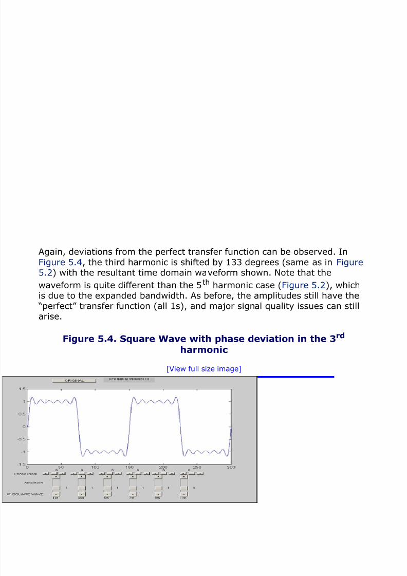
8/10/2019 eetop.cn_Power Integrity for IO Interfaces.pdf
http://slidepdf.com/reader/full/eetopcnpower-integrity-for-io-interfacespdf 160/439
Again, deviations from the perfect transfer function can be observed. In
Figure 5.4, the third harmonic is shifted by 133 degrees (same as in Figure5.2) with the resultant time domain waveform shown. Note that the
waveform is quite different than the 5th harmonic case (Figure 5.2), whichis due to the expanded bandwidth. As before, the amplitudes still have the
“perfect” transfer function (all 1s), and major signal quality issues can stillarise.
Figure 5.4. Square Wave with phase deviation in the 3rd harmonic
[View full size image]

8/10/2019 eetop.cn_Power Integrity for IO Interfaces.pdf
http://slidepdf.com/reader/full/eetopcnpower-integrity-for-io-interfacespdf 161/439
The final example for the Fourier series shows a case where the transfer
function has a resonance. In Figure 5.5, the 5th harmonic in this squarewave is multiplied by 2; this would be a resonance condition (pole in thefrequency domain). Also, note the phase is also shifted in this example. The
time domain waveform shows a large amount of ringing at the 5th harmonic(as expected).
Figure 5.5. Square Wave with phase and amplitude deviation in
the 5th harmonic
[View full size image]

8/10/2019 eetop.cn_Power Integrity for IO Interfaces.pdf
http://slidepdf.com/reader/full/eetopcnpower-integrity-for-io-interfacespdf 162/439
The Fourier series as explained before is useful for a general understanding
of the frequency domain concepts but is not the entire picture. The Fouriertransform provides the rest of the picture and enables the spectrum to befilled in between the harmonics and removes the restriction of a periodicwaveform.
5.1.1. Fourier Transform Interpretation
Fourier transform establishes the conceptual link between the time andfrequency domain. The Fourier series is applied for periodic (infinite extent)waveforms, but the ideas behind the Fourier series can be generalized tobecome a Fourier transform. This is done by allowing for a continuum offrequencies (not just harmonics) and moving from a series representationto an integral representation. The Fourier transform is applicable to large
subset of waveforms and does not require periodicity. The Fourier transformof a time domain waveform results in a spectrum once again, and thisspectrum now contains a continuum of frequencies, all with amplitude andphase “coefficients,” just like the Fourier series. The spectrum of a Fouriertransform is continuous (continuum of frequencies) as compared to the
“line” spectrum of a Fourier series. Note that if the waveform is periodic, aFourier transform yields a line spectrum identical to that of thecorresponding Fourier series.
The physical interpretation of the Fourier series spectrums versus a Fourier
transform spectrum is as follows: Fourier series produces “lines” (infinitespectral resolution), because the waveform is periodic and infinite. As youtruncate an infinite waveform, the lines begin to broaden and produce the

8/10/2019 eetop.cn_Power Integrity for IO Interfaces.pdf
http://slidepdf.com/reader/full/eetopcnpower-integrity-for-io-interfacespdf 163/439
Fourier transform spectrums. As the truncation is made more and moresevere, the broadening is increased until the point that a delta function(time domain), which is the most truncated time domain waveform,
produces an infinitely broad spectrum. (All frequencies are needed.)
This is the essence of the uncertainty principle in time-frequency analysis.
Also, it is one of the reasons why we do frequency domain analysis in thefirst place and follow it with time domain (transient) simulations as well.This is because a time domain response provides an excellent resolution inthe time domain, which as explained earlier, would be difficult to obtain inthe frequency domain (need a lot of frequency points). The converse is alsotrue; a frequency domain response provides perfect resolution in thefrequency domain, whereas a time domain waveform would take aprohibitive amount of time to simulate at that resolution.
For real-world applications a continuum of frequencies is impossible;therefore, it is necessary to discretize the frequencies (just like we do in thetime domain with a time step). This results in a Discrete Fourier Transform(DFT) and a special form of the DFT is the Fast Fourier Transform (FFT).
The important concept to remember is that the time steps (in the timedomain) are inversely related to the frequency steps in the frequencydomain. This is another statement of the uncertainty principle. Thefrequency resolution can still be improved (even with a small time step), byincreasing the number of points, by zero padding, or simulating a longer
time domain response.
5.1.2. Important Properties of the FourierTransform
This section lists some of the important properties of the Fourier transform;note that this information can be found in numerous textbooks along withadditional properties and transform pairs.
5.1.2.1. Interpreting and Using Frequency DomainRepresentations of Waveforms
A spectrum y(f) is in general a complex (real and imaginary). The commonplot of a spectrum is the power spectral density (PSD) which is 20 * log(abs(y(f)). This plot gives information only for the magnitude of the spectrum,however, the phase portion is also important. The Fourier transform of areal valued (typical) time domain waveform produces a spectrum withnegative frequency components (y(f) = y(–f)*). A common practice is todisplay only the positive frequencies. It is important to include the negative
frequencies when computing the inverse Fourier transform.
5.1.2.2. Key Properties of Fourier Transforms (of Interest in

8/10/2019 eetop.cn_Power Integrity for IO Interfaces.pdf
http://slidepdf.com/reader/full/eetopcnpower-integrity-for-io-interfacespdf 164/439
SI)
Convolution in time domain is multiplication in frequency domain :: x(t) * z(t) = X(f)Z(f)
Linearity :: ax(t) + bz(t) = aX(f) + bZ(f)
Time delay/Phase shift :: x(t-a) = X(f)exp(–j2πf*a)
Rectangular waveform in time domain is sinc function in frequencydomain (and vice versa)
Triangular waveform in time domain is sinc^2 function in frequencydomain
Trapezoidal waveform is corresponding to sinc(A)*sinc(B)
Impulse in time domain is a flat spectrum (–inf to inf) in freq.
Impulse in freq domain is infinite sinusoid in time domain.
Impulse train in time domain is impulse train in frequency domain(used with convolution delta functions).
5.1.2.3. Fourier Transform Examples and Interpretation
The power spectral density (PSD) is the common means of displayingspectrum magnitudes. The PSD of random bit patterns are shown in Figure5.6, where various (random) 100-bit sequences of perfect square pulses areFourier transformed. This plot is overlayed with the theoretical, sinc(F*T/2)(F=Freq, T=bit period) PSD along with certain deterministic cases (Fastest101010101..., ½ Fastest 11001100... and slowest 0000000...11111....).The respective time domain waveforms can be seen in Figure 5.7, where
top to bottom plots are the slowest, ½ fastest, fastest, and then onerandom bit pattern. The PSD in Figure 5.6 is for a 33MHz (max freq) bus,where the odd harmonics are seen to be maximal points and the evenharmonics are nulls. This plot illustrates the need for frequency domainanalysis to “fill” in the spectral coverage that time domain bit patterns leave
out, when they are not exhaustively simulated. Also of importance is theedge rate was not included in this example.
Figure 5.6. PSD of random bit patterns (Square Wave)

8/10/2019 eetop.cn_Power Integrity for IO Interfaces.pdf
http://slidepdf.com/reader/full/eetopcnpower-integrity-for-io-interfacespdf 165/439
Figure 5.7. Time domain waveforms for random bit patternexample
The following examples look into the relationship of edge rate andbandwidth. The general concept that the edge rate is related to bandwidthwas discussed in the Fourier series section, where it was shown that alarger bandwidth signal resulted in faster edge rates. The following analysis
is performed using the Fourier transform on just a single pulse (not periodicwave). In Figure 5.8, the PSD for two triangular pulses (in the time domain)are shown in the solid lines, and two trapezoidal pulses in the dashed lines.

8/10/2019 eetop.cn_Power Integrity for IO Interfaces.pdf
http://slidepdf.com/reader/full/eetopcnpower-integrity-for-io-interfacespdf 166/439
The rise time (edge rate) was varied to show the impact in the frequencydomain. The faster the edge rate, the larger the bandwidth, as seen withthe 0.7ns rise time versus the 1.2ns rise time.
Figure 5.8. PSD of various pulse shapes
The trapezoidal waveform though does not require the same amount ofbandwidth that the triangular wave requires. This can be seen from themathematical descriptions of the spectrums. From the properties of theFourier transform, the triangular pulse is corresponding to sinc(Tr)*sinc(Tr)(not exact equations just to show relationship), whereas the trapezoidalpulse is corresponding to sinc(Tr)*sinc(pw), where pw>Tr, therefore thesinc(pw) term modulates the sinc(Tr) and reduces (because pw>Tr) thebandwidth.
Also of importance is that the amplitude of the time domain waveforms
does not impact the Fourier transforms (linearity), other than the amplitudeof the transform.
The analysis on the pulse spectrums can be extended by sweeping the risetime for the triangular waveform. In Figure 5.9, the rise times are sweptfrom 0.1ns to 2.0ns, with the resulting PSD dB contours shown. The rule ofthumb for edge rate to bandwidth is 1/(π * rise time) and we see that thiscorrelates to the 3dB points of this waveform. We also observe thedependence on rise time (Tr) changes significantly as the rise time goesbelow 1ns, as expected.
Figure 5.9. dB contours of PSD for triangular pulses with variousrise times, overlayed with the 1/(π×Tr) approximation

8/10/2019 eetop.cn_Power Integrity for IO Interfaces.pdf
http://slidepdf.com/reader/full/eetopcnpower-integrity-for-io-interfacespdf 167/439
[View full size image]
The dependence on pulse width (pw) is shown in Figure 5.10, where anominal rise time of 1ns is assumed for all cases as the pulse width is sweptfrom 2ns (triangular) to 14ns. We observe that the pulse width decreasesthe bandwidth of the pulse and that the 2ns pulse width correlates to thetriangular wave, as expected. The other observation is that the firstsidelobe becomes more and more important as the pulse width is increased,this is physically the effect of the edge rate and tends to create a need for a
higher effective bandwidth (more in line with the triangular pulse) tocapture the sidelobe.
Figure 5.10. dB contours of PSD for trapezoidal pulses withvarious pulse widths (Tr = 1ns), overlayed with the 1/(π×Tr)
approximation
[View full size image]

8/10/2019 eetop.cn_Power Integrity for IO Interfaces.pdf
http://slidepdf.com/reader/full/eetopcnpower-integrity-for-io-interfacespdf 168/439
From these plots various metrics can be defined to determine a frequencydomain specification. For example, if a 1ns risetime (convert to slew rate ifnecessary) is required at a receiver, the channel must pass at least 600MHzto meet a –10dB specification, provided that the driver can transmit a 1nsrisetime waveform. The frequency domain response of the channel wouldthen be used to ensure the proper bandwidth is available (and wellbehaved).
5.1.2.4. Trapezoidal Pulse Fourier Transform Tool
To study the relationship between the time and frequency domain, a genericsoftware tool has been created that provides an interactive environment toexplore these concepts. Figure 5.11 shows the basic interface, where threelarge plots show the time, magnitude (Freq), and phase (Freq) plots for agiven signal. The user can add up to two poles/zeros and observe theeffects in the time and frequency domains as compared to the ideal case.This tool can be thought of as representing the transfer function of thesystem, with the driver and the receiver side curves. However, when
applying deviations to the phase and magnitude, a casual relationship is notenforced.
Figure 5.11. Software tool for Fourier transform concepts
[View full size image]

8/10/2019 eetop.cn_Power Integrity for IO Interfaces.pdf
http://slidepdf.com/reader/full/eetopcnpower-integrity-for-io-interfacespdf 169/439
In this example, a pole is added at 500MHz with a Q (width) of 100MHz anda relative amplitude of 3.045; also a zero is added at 400MHz with a Q of50MHz; the effects on a 1V/ns edge are shown. Also, note that the fallingedge is 0.5V/ns. The effects on the rising edge are significant, where as thefalling edge does not require the bandwidth that the leading edge does andis not impacted as much.
This example represents the type of information obtained in the frequencydomain (the bottom two plots) and how it can be interpreted.
A similar example can be observed (same poles/zeros) when the waveformhas been extended (periodically). Note that the spectrum is now much morecomplicated and Inter Symbol Interference can now play a major role.Figure 5.12 shows the properties of the Fourier transform—pulse train.
Figure 5.12. The properties of the Fourier series for pulse train
[View full size image]

8/10/2019 eetop.cn_Power Integrity for IO Interfaces.pdf
http://slidepdf.com/reader/full/eetopcnpower-integrity-for-io-interfacespdf 170/439
This brings up an important concept for the interpretation of spectrum. Itwas shown earlier how pulse width modulates the spectrum. The example inFigure 5.12 is similar to a pulse train, which also modulates the spectrum.The time domain waveforms with edges (transitions) followed by a DC levelin between, could be thought of as sending a burst of frequencies (edge)followed by DC.; However, when we perform a Fourier transform on theentire pulse (or bit pattern), we apparently lose the spectral content for theindividual edges. This can be visualized in Figure 5.13, where a short time-interval Fourier transform was performed on the time pulse above it. Wesee that the leading edge (0.5ns risetime) produces localized burst highfrequencies. When this is compared to the falling edge (1.0ns falltime) wesee the reduced spectral content. Note that the pulse width did not lowerthe bandwidth (as predicted in Figure 5.10), whereas a composite Fouriertransform would have lowered it.
Figure 5.13. Short time Fourier transform of a pulse
[View full size image]

8/10/2019 eetop.cn_Power Integrity for IO Interfaces.pdf
http://slidepdf.com/reader/full/eetopcnpower-integrity-for-io-interfacespdf 171/439
As we modulate (convolve) waveforms, the edge contribution is apparentlyreduced. This is actually not the case, it is just a result of the modulatingwaveform emphasizing a certain region (lower frequencies) and this mustbe accounted for. This impacts the specifications and simulationmethodologies needed to correctly interpret the spectra.
5.1.3. FFT of Power Noise
In Chapter 2, “I/O Interfaces,” current profiles in the PDN for various single-ended and differential systems are shown. This current goes through thePDN that may have resonances in the impedance response. As a result, thenoise is produced in the PDN. Figure 5.14 shows one example of the PDN
noise of which the FFT is taken. It demonstrates the SSO noise spectrum ofDDR333 with a pattern 101010. The major frequency components are333MHz as the second harmonic of the data signal, 167MHz being thefundamental frequency, 500MHz as the third harmonic, and 666MHz as thefourth harmonic. Similarly for the DDR800, we could expect that the major
components are 400MHz, 800MHz, 1200MHz, and 1600MHz, respectively.
Figure 5.14 shows two cases of on-chip decoupling capacitors: 50pF/IO and200pF/IO. Various frequency components are visible in the frequencydomain FFT plot. For 200pF/IO, the major component seen is at 167MHz.For 50pF/IO, the major component seen is at 333MHz; however, there arealso other components such as 500MHz and 667MHz. For higher on-chipcapacitance, the impedance at higher frequency is low, and hence, in turn,the power noise at the higher frequency is low. Therefore, for 200pF/IOcase, the prominent frequency seen is 167MHz, and other frequencies havelow magnitude. The intent of this graph is to show various frequencycomponents in the power noise. In comparison with the dark dotted line of
the 50-pF decoupling capacitor per each buffer, the light dotted linerepresents that the on-die decoupling capacitor is effective for high-frequency noise reduction.

8/10/2019 eetop.cn_Power Integrity for IO Interfaces.pdf
http://slidepdf.com/reader/full/eetopcnpower-integrity-for-io-interfacespdf 172/439
Figure 5.14. FFT of PDN noise (measured)
5.1.4. Convolution and Filtering
Consider that when the time domain input waveform x(t) passes through asystem with transfer function h(t), it results in the time domain outputwaveform y(t). These x(t) and h(t) time domain functions are integrablewith Fourier transforms resulting in X(f) and H(f). The functions X(f) and H(f) are frequency domain representations of the input waveform andtransfer function, respectively. The Fourier transform of the convolution is Y(f) = F{x(t)*h(t)}, where F is the Fourier operator and Y(f) is outputwaveform in frequency domain (see Figure 5.15). Y(f) is the product ofFourier transforms X(f) and H(f), thus, Y(f) = X(f) H(f).
Figure 5.15. Signal and system frequency response
It is important to realize that filtering is also a convolution. An example is
shown in Figure 5.16, where a step response is convolved with the transferfunction of a channel. The upper plot shows the transfer function H(f),which is obtained in the frequency domain, for two cases of a topology. Thelower plot is the time domain waveform of the transfer function convolvedwith a step response. Mathematically, this is the output waveform y(t)=IFFT{X(f)H(f)}, where X(f) = 1/(j*2πf) and H(f) is the transfer function. Itshows that a larger bandwidth transfer function produces a faster edge rate.Note this can also be viewed from the filtering standpoint, in that H(f) is thelow-pass filter response.
Figure 5.16. Convolution example

8/10/2019 eetop.cn_Power Integrity for IO Interfaces.pdf
http://slidepdf.com/reader/full/eetopcnpower-integrity-for-io-interfacespdf 173/439

8/10/2019 eetop.cn_Power Integrity for IO Interfaces.pdf
http://slidepdf.com/reader/full/eetopcnpower-integrity-for-io-interfacespdf 174/439
No part of any chapter or book may be reproduced or transmitted in any form by any means withoutthe prior written permission for reprints and excerpts from the publisher of the book or chapter.Redistribution or other use that violates the fair use privilege under U.S. copyright laws (see 17USC107) or that otherwise violates these Terms of Service is strictly prohibited. Violators will be
prosecuted to the full extent of U.S. Federal and Massachusetts laws.
5.2. Signal and Power Integrity Applications
Frequency domain techniques can be effectively used in signal and powerintegrity applications. Scattering parameters are commonly used for thefrequency domain analysis. Electromagnetic simulation tools have S-parameters as output, for signal nets and for power nets. S-parameters can
be converted into Y- or Z-parameters as discussed in Chapter 3, “Electromagnetic Effects.” The following section lists the commonly used S-and Z-parameters for signal and power integrity analysis:
Self-impedance of the power net: Z11
represent the self-impedance
of the power net, which is the primary design parameter for PDNdesign in the frequency domain. It is corresponding to the PDN noise inthe time domain.
Coupling from other power nodes: If two different ports connect tothe same power domain at different locations, Z
21 represents the
transfer impedance of the power net. It is an indicator of coupling frompower node 1 to power node 2. This coupling factor can be used in SSOanalysis.
SSO in frequency domain: Typically, the SSO is the time domainphenomenon, however, it can also be analyzed in the frequencydomain. Z
Tot is the total impedance for a node on a distributed PDN. It
accounts for self-impedance Z11 and the summation of transferimpedances Z
21 from the neighboring nodes. This is useful for
determining the SSO impact in the frequency domain. One of theassumptions is that the amplitude and phase of the currents ondifferent nodes are similar.
Coupling between two power domains: If the port 1 connects toone power domain and port 2 connects to other power domain, thecoupling between them is determined by the voltage transfer function
Z21 / Z11. It is corresponding to the domain-to-domain noise couplingin the time domain.

8/10/2019 eetop.cn_Power Integrity for IO Interfaces.pdf
http://slidepdf.com/reader/full/eetopcnpower-integrity-for-io-interfacespdf 175/439
Power-to-signal coupling: If the port 1 connects to power net andport 2 connects to signal net, transfer impedance Z
21 describes the
coupling from the power to the signal net. Power-to-signal coupling canbe determined at different locations such as a chip location or PCBlocation.
Return loss: If the port 1 connects to the signal net, the return loss ofa signal net is characterized by S
11. It is corresponding to the reflection
coefficient at port 1.
Insertion loss: For a signal net, if the port 1 connects to the driverend and port 2 connects to the receiver end, the insertion loss of thesignal net is S
21.
Crosstalk: Transfer impedance (Z12
) is an indicator for crosstalk
between two signal nets. It is especially true for signaling schemeswhere the current is flowing on the transmission line to the far end.The voltage coupled to adjacent signal net due to the current in a givensignal net is determined with Z
12. Consider that the nets A and B are
routed from the driver to receiver. Port 1 is connected to the net A andport 2 is connected to the net B. For the near end crosstalk, port 1 and2 are on the same side (for example, driver side). For the far endcrosstalk, port 1 is on one side (for example, driver side) and the port2 is on the other side (for example, receiver side).
ISI: Voltage transfer function is an indicator of an ISI. It is determinedby Z
21 / Z
11, where port 1 connects to the driver side signal net and
port 2 connects to receiver side of the same signal net. Typically it isrecommended to have a flat voltage transfer function in the givenfrequency range of operation.
5.2.1. S-Parameters with Global and Local Ground
For a signal or a power port, there is a positive and a negative terminal. Insome simulators, all the negative terminals connect to a certain referencepoint. These simulators have separate ports for signal and local ground, asshown in Figure 5.17.
Figure 5.17. S-parameter model with local ground ports

8/10/2019 eetop.cn_Power Integrity for IO Interfaces.pdf
http://slidepdf.com/reader/full/eetopcnpower-integrity-for-io-interfacespdf 176/439
There is a signal at port P1 with its reference at port P3. At the far end, thesignal is at port P2 with its reference at port P4. For example, this networkis generated for a signal net on the PCB from the driver end (port P1) to thereceiver end (port P2). This signal is referenced to the ground. Port P3 isconnected to the local ground near port P1, and port P4 is connected to thelocal ground near port P2. All the negative terminals of ports P1 through P4are connected to the reference terminal. The resultant S-parameters for thisnet have four ports and a reference node.
When the equivalent circuit is created, it will have four terminals, T1
through T4, corresponding to P1 through P4, along with a reference node.This reference is typically connected to the global ground of the circuitsimulator. The global ground is a reference point for all voltagemeasurement in the system that it becomes ideal sink for all currents. Inthis type of S-parameters, the voltage variations between different grounds(driver side ground and receiver side ground) can be analyzed.
Often, the delta variation between a signal or power port and its referencenode is adequate for the analysis. In the lab, when measurements areperformed, they always reference to a local ground. For the second type of
S-parameters, there are only terminals for signal or power nets, as shownin Figure 5.18.
Figure 5.18. S-parameters model without local ground ports

8/10/2019 eetop.cn_Power Integrity for IO Interfaces.pdf
http://slidepdf.com/reader/full/eetopcnpower-integrity-for-io-interfacespdf 177/439
In this example, the negative terminal of the port is connected to a closest
point on the return path. The positive terminal of port P1 is connected tosignal (driver end), and the negative terminal connected to the localground, where the positive terminal of port P3 was connected before.Similarly, the negative terminal of port P2 connected to the local ground,where positive terminal of port P4 connected before. The resultant S-parameters have only two ports with a reference node. The equivalent
circuit has two terminals with a reference node. In this type of S-parameters, the reference node is arbitrary and does not have any physicalmeaning. The advantage of this type of S-parameters is that it has a lowernumber of ports. The disadvantage is that it cannot measure the response
from one local ground node to the other local ground node.
When using different types of S-parameters in a circuit simulator, propercare has to be taken to connect the local ground ports, if any, and thereference ports [1]. Consider that there are two different types of S-parameters to be used in a system simulation. The first one is, for example,for the on-chip PDN and has the power ports and local ground ports, with a
reference node, as shown in Figure 5.17. Second set of S-parameters, forexample, is for the package PDN, which has only power terminals with areference node, as shown in Figure 5.18. When using these two differenttypes of S-parameters, one cannot connect all the local ground ports fromthe on-chip PDN S-parameters to the reference node of the package PDN[2]. It will imply that all the local ground terminals for the on-chip PDN are
shorted, which is not accurate. One of the ways to make the modelscompatible is to regenerate S-parameters of the on-chip PDN with onlypower ports. It can be done by taking the S-parameter model for the on-chip PDN and redefining the ports. For example, the on-chip model withports P1, P2, P3, and P4 is converted to the newer model with ports P1 andP2, whereas the negative terminals of ports P1 and P2 are connected to
local grounds. The newly generated S-parameters have a reference nodethat can be connected to the reference node of the package S-parameters.

8/10/2019 eetop.cn_Power Integrity for IO Interfaces.pdf
http://slidepdf.com/reader/full/eetopcnpower-integrity-for-io-interfacespdf 178/439
S-parameters can be expressed in the Touchstone® format. S-parametershave the port impedance, but Y- and Z-parameters are independent of portimpedance. For the signal net, the typical port impedance is 50Ω. This 50Ω is typical for RF designs, and the traces on the PCB are typically designed tohave a 50Ω characteristic impedance. For the power net, the characteristic
impedance is much lower than 50Ω. In the Touchstone®
1.0 format, onlyone value of port impedance can be used for all the ports; however, for
Touchstone® 2.0, different port impedances can be used for different ports[3].

8/10/2019 eetop.cn_Power Integrity for IO Interfaces.pdf
http://slidepdf.com/reader/full/eetopcnpower-integrity-for-io-interfacespdf 179/439
No part of any chapter or book may be reproduced or transmitted in any form by any means withoutthe prior written permission for reprints and excerpts from the publisher of the book or chapter.Redistribution or other use that violates the fair use privilege under U.S. copyright laws (see 17USC107) or that otherwise violates these Terms of Service is strictly prohibited. Violators will be
prosecuted to the full extent of U.S. Federal and Massachusetts laws.
5.3. Power Distribution Network Design inFrequency Domain
The important design parameter for the power distribution network designin frequency domain is the self-impedance or Z
11.
Equation 5.3
Z11
is a single port parameter and shows the relationship between the
resultant voltage at the PDN port due to the input current at that port.Input current for the PDN is transient in nature and may contain differentfrequency components. It depends on the circuit blocks on the power
domain. As shown in Chapter 2, the I/O interface has different circuit blockssuch as
Logic circuits: The interface with the core.
High speed I/O circuits: These circuits include clocking circuits andcircuits for prior to final stage.
Final stage circuits: Comprise driver and receiver circuits.
For an I/O interface, the designer may choose to have only one powerdomain for all these blocks. If some blocks are sensitive to noise, the
designer may choose to have separate power domains for those blocks. It
Where Z 11
= Self-impedance
V = Power supply voltage
Δv = % Ripple
I max
– I min
= Transient current

8/10/2019 eetop.cn_Power Integrity for IO Interfaces.pdf
http://slidepdf.com/reader/full/eetopcnpower-integrity-for-io-interfacespdf 180/439
depends on the cost-performance trade-off because a different domainimplies that there will be a different regulator and different routingschemes. In some applications, there may be the same domain on the PCB
but separated out through a filter before going to the package.
5.3.1. Impedance Response Z11
As shown in the Chapter 3, there are different peaks due to the resonancesin the power deliver network. A simplified RLC network of the entire powerdelivery network is shown in Figure 5.19.
Figure 5.19. Simplified power delivery network
[View full size image]
There is a voltage source and corresponding inductance. Then on the PCBthere is a bulk capacitor C
bk
and a ceramic capacitor Cbd
. Then there is a
package capacitor Cpk
. Cpl
illustrates the plane-to-plane decoupling
capacitor on the board and package. Then there is on-chip capacitor Cdie
.
There are resistances and inductances in between the capacitors. Thisinductance is similar to spreading inductance of the plane, as described inChapter 4, “System Interconnects.”
Figure 5.20 shows the Z11
plot looking from the die of the I/O buffer. This
plot is generic in nature and in the preceding network; only 1 bulk
capacitor, 1 edge capacitor, and 1 package capacitor is used for illustrationpurposes. This is the open circuit response probed at the die. Threeresonant peaks are shown in the figure. Voltage source is not used, so theimpedance is very high at the DC point.
Figure 5.20. Self-impedance of the PDN

8/10/2019 eetop.cn_Power Integrity for IO Interfaces.pdf
http://slidepdf.com/reader/full/eetopcnpower-integrity-for-io-interfacespdf 181/439
Effective frequency range of board edge capacitor is from 1MHz to tens ofMHz. The first slope is due to the bulk capacitor C
bk, which is effective in
the kHz to MHz range. It has a flat response at low frequencies. Theeffective frequency range of the board ceramic (edge) capacitor is from1MHz to tens of MHz, and the package capacitor is from tens of MHz to afew hundreds MHz. The chip capacitor can be effective all the way to a veryhigh frequency range. The first resonant peak is due to the board
inductance and the board ceramic capacitor Cbd. The second resonant peakis due to the board and package inductance and the package capacitor C
pk.
The package inductance in this case is from the package BGAs (connectionpoint to the board) to the package capacitor. The third and prominent peakis due to the package inductance and die capacitance. This inductance isfrom the package capacitor to the die. With proper design and decouplingcapacitor optimization, these peaks can be reduced or shifted.
Cpl
, the plane capacitance, is low in value and is effective for high
frequencies. In the preceding network, the impedance is probed at the dielocation, and the C
pl is separated inductively from the die. Also, there is the
Cdie
that has much more value than Cpl
. Therefore the effect of this Cpl
capacitor is overshadowed when looking from the die. However, if we probeonly the impedance on the board or package, the effect of C
pl will be more
vivid. When 3D or planar 3D electromagnetic models are used for the boardand package, the effects of C
pl and spreading inductance are captured
accurately.
When the voltage source or VRM is used, the low frequency impedance isshort circuit or very low. With multiple bulk and ceramic capacitors, the firsttwo peaks can be reduced substantially. Consider that with the optimized

8/10/2019 eetop.cn_Power Integrity for IO Interfaces.pdf
http://slidepdf.com/reader/full/eetopcnpower-integrity-for-io-interfacespdf 182/439
capacitors on the PCB, package and die, the impedance response lookingfrom the die is as shown in Figure 5.21. The maximum impedance at theresonance is about 0.18Ω [5]. For this simulation, planar 3D
electromagnetic models for the package and PCB PDN are used.
Figure 5.21. Z11
of the optimized PDN
Source: V. Pandit, A. N. Pardiwala, Hsiao-ching Chuang, M. J. Choi, Md. R. Quddus, “SSO Noise,Eye Margin, and Jitter Characterization for I/O Power Integrity,” DesignCon 2009.
5.3.2. Impedance Targets for I/O Interface
To determine the impedance target, it is important to evaluate the timedomain response to different excitations. The noise is simulated at the dielocation when different excitations are subjected to the preceding powerdelivery network. In the frequency domain, the following PDN impedance
formula can be used:
Equation 5.4
Where the following are the function of frequency
Z11
(f) = Impedance
V(f) = Voltage noise
I(f) = Current

8/10/2019 eetop.cn_Power Integrity for IO Interfaces.pdf
http://slidepdf.com/reader/full/eetopcnpower-integrity-for-io-interfacespdf 183/439
Equation (5.4) also can be written as
Equation 5.5
In the preceding equation, the phase and amplitude of the impedance andcurrent need to be considered. When there is only one frequency at240MHz, 1A peak-to-peak current produces 180mV peak-to-peak noise, asZ
11 at that frequency is about 180mΩ. If the nominal voltage is 1.5V, the
180mV peak to peak will be ± 6%. In other words, if the required toleranceis ± 6% for 1.5V nominal voltage, then at 240MHz the impedancerequirement is about 180mΩ (assuming 1A of current at that frequency).However, the currents in PDN are more complex in nature, as shown inChapter 2. In view of this, the impedance target needs to be calculatedtaking into account the overall spectrum. The impedance target can be
frequency-dependent; however, looking into the chip, the worst-case targetimpedance is calculated and can be applied to the wide band of frequencies.
There are different methods to achieve the target impedance on the PCB. Inthe Deep V method, the same capacitor type is used in multiple numbers to
achieve a deep V shape [6]. In a second type of method to achieve targetimpedance, about three capacitors are used per decade of frequencies. Inthe third method, known as Frequency Dependent Target Impedance
Method (FDTIM), the capacitors are selected at each value to achieve a flatline at target impedance. For the core circuits, the PCB capacitors may behigh in number [6], however for the I/O interfaces, the PCB capacitor
number is lower than that for the core. The impedance target at the chip ordie can be achieved with co-analysis of the PCB, the package, and the chipPD network.
The PDN impedance target depends on the required voltage tolerance and
current in the power domain. If only the final stage circuits are connected tothe power domain under design, the current in that domain is computed by
taking into account the possible activity for all the drivers and receivers inthe final stage. If there is more than one stage connected to the samepower domain, the combination of all the currents and their worst-caseactivity need to be considered.
5.3.2.1. Single-Ended Driver
As shown in Chapter 2 for a single-ended driver, current in the power andground varies in accordance with the bit pattern. The pattern can match thePDN resonance pattern at the highest peak, which is in the 100s of MHz
range. Suppose the maximum data rate is 1600MT/s, and there is a halfrate clock (800MHz), then the pattern 1111000011110000 has frequency of200MHz. It is close to the resonance frequency of the PDN described in the

8/10/2019 eetop.cn_Power Integrity for IO Interfaces.pdf
http://slidepdf.com/reader/full/eetopcnpower-integrity-for-io-interfacespdf 184/439
previous section. To determine the impedance target of the single-endedsystem, the worst-case pattern is considered. The current in the powerdomain may have different frequency contents [7]. The current is
determined in the PDN for the entire interface, and its FFT is taken. Fromthe FFT, the spectral contents are identified. The impedance target isdetermined based on the energy at particular frequency.
In an alternative approach, a preliminary power delivery network isconstructed. The current profile is determined for the entire bus when allthe bits are switching simultaneously at the resonance frequency. Then thiscurrent is subjected to the simple power delivery network model, and thenoise is determined. If the noise level is higher than expected, some keyelements such as an on-die capacitor is changed in the simple powerdistribution network model. In some iterations, the desired amount of noiseis obtained, and the impedance target is determined. In general, the
impedance is highest at the chip-package resonance frequency, so theimpedance target has to be met at that frequency.
5.3.2.2. Differential Driver
For a differential system, there are different types of differential drivers,such as pseudo differential and half differential, as shown in Chapter 2. Forboth of these driver types, the PDN current is typically at high frequenciesfor normal operation. There is little variation in the current depending onthe data pattern. However, whenever there is a “power on” for a differential
bus, there is a big step for the current [8]. After this step, there is a normaloperation current. For determining the impedance target for a differentialsystem, two scenarios need to be considered. First is the normal operationcondition. In this condition, the bus runs at a normal operation and has aPDN current at the bus operation frequency, say 2.5GHz. The PDNimpedance at 2.5GHz needs to be considered. In the second scenario, thebus is powering on or off. In this scenario, there is a DC step of current.There is droop when the buffers are powered on, and there is a bouncewhen the buffers are powered off. This droop or bounce magnitude isdependent on the amplitude of the Z
11 at the PDN resonance. After the
droop or bounce, there is a ringing before the noise settles down. Thisringing frequency is dependent on the resonance frequency of Z
11.
5.3.2.3. Prior Stages
Clocking circuits are part of high-speed I/O circuits for single-ended anddifferential system. The different clocking schemes such as Phase LockedLoop (PLL) or Delay Locked Loop (DLL) can be used. The current in the
power domain for those schemes depends on whether the clock is single-
ended or differential. The current varies in the PDN of the clock circuitsaccording to the topology. Although final stage driver circuits may switch atdifferent data rates, clocking circuits have only specific data rates.

8/10/2019 eetop.cn_Power Integrity for IO Interfaces.pdf
http://slidepdf.com/reader/full/eetopcnpower-integrity-for-io-interfacespdf 185/439
Other examples of high speed I/O circuits before the final stage are a phaseinterpolator, a parallel to serial converter, a predriver, depending on theinterface. The change in current in the power domain for these circuits may
or may not be data-dependent. There is also logic block in the I/O interface,which communicates with the processing unit. The activity for the logicassociated with this block is determined to get the current in the powerdomain.
If the final stage and other stages are on the same power domain, then thecurrent profile in power domain may have a variety of different frequencies.Consider a PDN comprising of a PCB, a package, and a single-node diemodel. The target impedance, looking from the die location, serves as apreliminary design target. In the single-node die model, all the current isinjected into one node, and the voltage noise is determined. In a distributeddie model, there is a variation from node to node at different locations of
the die.
As shown in subsequent sections, different PDN elements such as the PCB,package, and die influence different frequency range. For individualcomponents, the target impedance needs to be maintained only for thefrequency range within which the component can have an effect. As anexample, the PCB can influence only up to a few tens of MHz, so the targetimpedance for the PCB components needs to be maintained within a fewtens of MHz of frequency. Beyond that frequency, it may exceed the targetimpedance, but there are other considerations, such as EMI mitigation.
5.3.3. PDN Design Example
Consider that the impedance target for an I/O interface is determined to be
200mΩ at the die location. This is much higher than typically required forthe core PDN. However, I/O interfaces have much lower current than thatfor the core. The overall PDN design methodology is similar, but the amountof decoupling may be different. In this example, the final stage driver andsome other stages like the predriver are on the same power domain underconsideration. As shown in Figure 5.22, the power distribution network
comprises the chip, package, and board networks [5].
Figure 5.22. Power delivery network
[View full size image]

8/10/2019 eetop.cn_Power Integrity for IO Interfaces.pdf
http://slidepdf.com/reader/full/eetopcnpower-integrity-for-io-interfacespdf 186/439
5.3.3.1. Package and PCB PDN
The board and package power distribution networks are modeled using 3D
or planar 3D electromagnetic solvers, and S-parameters are extracted.Then, the S-parameters are converted into Z-parameters and plotted for
impedance response. The plane-to-plane capacitance and plane inductanceis taken into account as the model is an electromagnetic based model. Thepackage Z-parameters response is shown in Figure 5.23.
Figure 5.23. Package PDN: Z11
simulation and correlation
Source: V. Pandit, A. N. Pardiwala, Hsiao-ching Chuang, M. J. Choi, Md. and R. Quddus, “SSO Noise, Eye Margin, and Jitter Characterization for I/O Power Integrity,” DesignCon 2009,
Presentation.
The plot shown in the graph is for the Z11
simulated and measured at the
package bump location of the power distribution network. The simulatorused is a planar 3D electromagnetic simulator. The measurements are donewith Vector Network Analyzer using a two-port method [9]. The simulationscorrelate well with the measurements. This Z
11 is for a pair of power and
ground bumps, and the curve is becoming inductive at 500MHz and again
capacitive above 900 MHz. When considering the entire interface forsimulations, all the die side bumps are considered as a lumped port. Itexhibits lower inductance than that for 1 bump.
Figure 5.24 shows the Z11
response at the package bump when the
package and PCB are analyzed together. Similar to the package, the PCB ismodeled with the planar 3D electromagnetic simulator. It has two ports: thepackage side BGA and the VRM port. For the first port, the package BGAside power distribution ports on the board are lumped into one port. The
VRM bulk capacitor is modeled when extracting the S-parameters for theboard. Then, the S-parameters of the board are cascaded with that for thepackage. There is no other decoupling capacitor than the VRM capacitor.

8/10/2019 eetop.cn_Power Integrity for IO Interfaces.pdf
http://slidepdf.com/reader/full/eetopcnpower-integrity-for-io-interfacespdf 187/439
The self-impedance of the package bump side port shows that for most ofthe frequencies above 10MHz, the impedance target of 200mΩ is exceeded.
Figure 5.24. Simulated Z11
with PCB and the package, no
capacitors
Source: V. Pandit, A. N. Pardiwala, Hsiao-ching Chuang, M. J. Choi, and Md. R. Quddus, “SSO Noise, Eye Margin, and Jitter Characterization for I/O Power Integrity,” DesignCon 2009.
5.3.3.2. PDN Co-Design: PCB, Package and Chip
The design target of 200mΩ needs to be achieved over a wide frequency
range. Different decoupling solutions affect different frequency range. Theresponse of the PCB and package PDN, looking from the package bump port
shows that the target is not met at many frequencies. In the PDN co-designapproach, the PCB, the package, and later the chip simulatedsimultaneously and decoupling solutions are optimized [5]. First, thedecoupling capacitors are placed on the PCB and optimized for the desiredfrequency response. Bulk capacitors are effective in low frequency from kHz
to several MHz, as shown in Figure 5.25a. This impedance is simulated fromthe package bump side for the cascaded package and board powerdistribution network. Then the high-frequency ceramic capacitors are placed
on the board near the package. Their effective frequency is a few 10s ofMHz. With the bulk capacitors and ceramic capacitors on the board, thetarget impedance is met in the 80MHz of frequency range, as shown in
Figure 5.25b. This impedance is simulated at the package bump side in thecascaded package and PCB network. PCB PDN decoupling cannot supporthigh-speed I/O currents, with faster rise times. For that, package leveldecoupling or chip level decoupling is required.
Figure 5.25. Simulated Z11
with PCB + PKG a) bulk caps; b) bulk
caps + edge caps
Source: V. Pandit, A. N. Pardiwala, Hsiao-ching Chuang, M. J. Choi, and Md. R. Quddus, “SSO

8/10/2019 eetop.cn_Power Integrity for IO Interfaces.pdf
http://slidepdf.com/reader/full/eetopcnpower-integrity-for-io-interfacespdf 188/439
Noise, Eye Margin, and Jitter Characterization for I/O Power Integrity,” DesignCon 2009.
Next, the package capacitors are placed, and the impedance is simulated atthe package bump location. The resultant plot is shown in Figure 5.26a. Thepackage capacitors are placed as close as possible to the die bump, so as to
minimize the inductance path from the die bump to the package capacitors.The target impedance is met in the frequency range of a few 100s of MHz.Above this frequency range only the chip capacitors are effective. With thechip capacitors, the target impedance of 200mΩ is met over the widefrequency range, as shown in Figure 5.26b. There is a resonance at around
240MHz, at which the impedance is maximum.
Figure 5.26. Simulated Z11
with (a) PCB and PKG caps, (b) PCB,
PKG, and chip caps
Source: V. Pandit, A. N. Pardiwala, Hsiao-ching Chuang, M. J. Choi, and Md. R. Quddus, “SSO Noise, Eye Margin, and Jitter Characterization for I/O Power Integrity,” DesignCon 2009.

8/10/2019 eetop.cn_Power Integrity for IO Interfaces.pdf
http://slidepdf.com/reader/full/eetopcnpower-integrity-for-io-interfacespdf 189/439
The on-chip PDN model used is shown in Figure 5.27. The on-chipdecoupling capacitor is C
die and its series resistance is R
die. R
leak is the
leakage resistance for that domain. From the bump to circuit location, thereis a power grid with parasitic resistances R
s and inductance L
s. The
sensitivity of Cdie
/Rdie
is shown in the Figure 5.28.
Figure 5.27. On-chip PDN model
Figure 5.28. Effect of on-chip PD elements on Z11
(simulated)

8/10/2019 eetop.cn_Power Integrity for IO Interfaces.pdf
http://slidepdf.com/reader/full/eetopcnpower-integrity-for-io-interfacespdf 190/439
Source: V. Pandit, A. N. Pardiwala, Hsiao-ching Chuang, M. J. Choi, Md. R. Quddus, “SSO Noise,Eye Margin, and Jitter Characterization for I/O Power Integrity,” DesignCon 2009, Presentation.
If Cdie
is lowered, the resonance peak increases and shifts toward the right.
If Rdie
is reduced, the resonant peak increases, but the high frequency
(>1GHz) impedance is lowered. There is a trade-off for the Z11
response for
high frequency and for low frequency.
5.3.4. On-Chip Power Delivery: Modeling andCharacterization
As shown in Chapter 4, the on-chip power delivery network is composed ofthe power grid, intentional capacitors, and unintentional or intrinsiccapacitors. It is difficult to characterize the power delivery network from thedie side because there are no access points on the die. Typically, the diemounted in the package is taken, and VNA measurements are done on thepackage pins. The package capacitors are removed. The package parasitics
are de-embedded and the on-chip model can be determined. Figure 5.29 shows the Z
11 measurement for the package pin and its equivalent model
simulations [5].

8/10/2019 eetop.cn_Power Integrity for IO Interfaces.pdf
http://slidepdf.com/reader/full/eetopcnpower-integrity-for-io-interfacespdf 191/439
Figure 5.29. Z11
for chip and package
Source: V. Pandit, A. N. Pardiwala, Hsiao-ching Chuang, M. J. Choi, and Md. R. Quddus, “SSO Noise, Eye Margin, and Jitter Characterization for I/O Power Integrity,” DesignCon 2009
The equivalent model topology is shown in Figure 5.27. In this case, Rs is
combination of the grid resistance and package resistance. Similarly, Ls is a
combination of grid inductance and package inductance. In the above
approach, it is difficult to separate out the Rdie and Rs from the measured
data. Similarly, due to the intentional chip capacitors, the amount of powergrid capacitor is difficult to estimate. So, with this approach, the power gridparasitics cannot be easily extracted from the measurement. Also, the C
die
is a combination of the intentional Cdie
and intrinsic Cdie
. With the
measurements described in Figure 5.29, the total Cdie
can be determined.
To characterize the on-chip power delivery network with power grid
parasitics, a special test vehicle can be designed. There are intentional on-chip capacitors and intrinsic on-chip capacitors. Power grid capacitance isone of the components of the intrinsic on-chip capacitance; the othercomponents are primarily due to circuits as described in Chapter 4. Withthis test vehicle, the power grid model and the on-chip intentionaldecoupling capacitor model can be extracted.
5.3.4.1. Test Vehicle for On-Chip PDN
The on-chip PDN is composed of the power grid and decoupling capacitors.
The following section presents a methodology for determining the on-chipPDN models with the test chip. A special test structure is designed tomeasure the S-parameter response for the on-chip PDN [10]. It has pad

8/10/2019 eetop.cn_Power Integrity for IO Interfaces.pdf
http://slidepdf.com/reader/full/eetopcnpower-integrity-for-io-interfacespdf 192/439
rows for measurement and the device under test, as shown in Figure 5.30.
Figure 5.30. Test Chip: Pad-row with the DUT
Source: V. Pandit, W. H. Ryu, S. Ramanujam, K. Pushparaj, and F. Fattouh, “Simulation andCharacterization of GHz on-chip Power Delivery Network,” DesignCon 2008.
There are two rows of the pad, and in each row, there are power pads andground pads. Power pads are surrounded by the ground pads on both sides.All the ground pads are connected together; however, the power pads areisolated from each other. Also, there is a ground shield placed between thepower pad and the ground pad. With this arrangement, the noise andextraneous effects are minimized during the VNA measurements up to10GHz and beyond.
There are different configurations of the test vehicle with the same pad-rowstructure. In each type, the DUT is different, as described here:
Pad-row with the open circuit power grid: For this structure, theDUT is only a multilayer power grid. This grid is not connected to anycapacitor. The size is very small (<200×200um).
Pad-row with short circuit power grid: For this structure, the DUTis a power grid with the power and ground nets of the grid shorted onthe lower metal layers.
Pad-row with the intentional capacitor: For this structure, the DUT
is a power grid with the intentional capacitor connected at the lowermetal layers.
For all the three structures, VNA measurements are performed up to40GHz. The power and ground pads are used for the VNA measurements.For the open circuit grid, the S-parameter is S
open and for short circuit grid,
it is Sshort
. With these two measurements, the 2×2 matrix for the power
grid S-parameters is constructed. The power grid is assumed to be asymmetric and reciprocal network: S
11grid = S
22grid and S
21grid = S
12grid.
Equation 5.6a

8/10/2019 eetop.cn_Power Integrity for IO Interfaces.pdf
http://slidepdf.com/reader/full/eetopcnpower-integrity-for-io-interfacespdf 193/439
Equation 5.6b
5.3.4.2. 2D TLM Empirical On-Chip PD Modeling Method
From the open circuit power grid structure, the capacitance andconductance of the grid are extracted, whereas from the short circuit powergrid structure, the resistance and inductance of the grid are extracted. Asimple RLGC model is created with these extractions, as shown in Figure
5.31. This model is similar to the transmission line model, and the powergrid can be constructed as a 2-dimensional transmission line matrix (2D
TLM).
Figure 5.31. RLGC model for power grid
Based on the design of the power grid, initial power grid parameters are
determined. The S-parameter response of the power grid are plotted andcompared against the measurements. The different parameters are tweakedto fit the response. The final model shows a good correlation to themeasured S-parameters up to 10GHz of frequency, as shown in Figure 5.32.Above that frequency, the lumped approximation is not valid.
Figure 5.32. S-parameters for the power grid
Source: V. Pandit, W. H. Ryu, S. Ramanujam, K. Pushparaj, and F. Fattouh, “Simulation andCharacterization of GHz on-chip Power Delivery Network,” DesignCon 2008.

8/10/2019 eetop.cn_Power Integrity for IO Interfaces.pdf
http://slidepdf.com/reader/full/eetopcnpower-integrity-for-io-interfacespdf 194/439
5.3.4.3. On-Chip Capacitor Model Extraction
The third type of structure in the test vehicle has an open circuit power gridand the on-chip intentional decoupling capacitor. This is the intentionalcapacitor that is designed with the transistor circuits. The measurementsare done on this structure with the VNA. The decoupling capacitor is
connected to the power grid, which in turn is connected to the pad. The S-parameters measured for the power grid + capacitor structure are S
11tot.
With a 2×2 S-parameter matrix of the power grid, the S11
of the decoupling
capacitor is computed as S11decap
:
Equation 5.7
A simple model of the transistor type on-die decoupling capacitor is created,as shown in Figure 5.33. It has the intentional capacitor C
die, its parasitic
resistance Rdie
, and the leakage resistance Rleak
.
Figure 5.33. Equivalent on-chip capacitor model

8/10/2019 eetop.cn_Power Integrity for IO Interfaces.pdf
http://slidepdf.com/reader/full/eetopcnpower-integrity-for-io-interfacespdf 195/439
Based on the design information, the initial parameters for this model aredetermined. These variables are changed to fit the curve for S
11. As shown
in Figure 5.34, it shows a good correlation up to a few GHz range.
Figure 5.34. Z11
for on-chip capacitor
Source: V. Pandit, W. H. Ryu, S. Ramanujam, K. Pushparaj, and F. Fattouh,” Simulation andCharacterization of GHz on-chip Power Delivery Network,” DesignCon 2008.
5.3.4.4. Modeling and Correlation for On-Chip PDN of the I/OInterface
As discussed in the previous section, the 2D TLM method for on-chip die
model includes the power grid model and decoupling capacitor model. Thismethod can be applied to the on-chip PDN model for the entire interface
[11, 12]. Figure 5.35 shows the on-chip geometry for the I/O interface.
Figure 5.35. On-chip geometry for I/O interface
Source: V. Pandit and W. H. Ryu, “Multi-GHz Modeling and Characterization of On-chip PowerDelivery Network,” EPEP 2008, Poster Presentation. © [2008] IEEE.

8/10/2019 eetop.cn_Power Integrity for IO Interfaces.pdf
http://slidepdf.com/reader/full/eetopcnpower-integrity-for-io-interfacespdf 196/439
It has different DQ Modules (DQM) as shown. The entire section is dividedinto different unit cells. Each unit cell is assigned a 2D TLM model asdiscussed in the earlier section. The unit cells are filled for the entiregeometry. The on-wafer probing is performed with the VNA at the bumplocation. The different PDN bumps are probed and the self-impedance andinsertion loss are plotted. The equivalent model with the 2D TLM methodshows a good correlation with the measurements, as shown in Figure 5.36.
Figure 5.36. Self-impedance and insertion loss for the on-chipPDN
Source: V. Pandit, and W. H. Ryu, “Multi-GHz Modeling and Characterization of On-chip PowerDelivery Network,” EPEP 2008, Poster Presentation. © [2008] IEEE.

8/10/2019 eetop.cn_Power Integrity for IO Interfaces.pdf
http://slidepdf.com/reader/full/eetopcnpower-integrity-for-io-interfacespdf 197/439
Note that the self-impedance plot shows the resistance of the network atabout 800mOhm. As described in earlier sections, it is a combination of thegrid resistance and the series resistance with the on-chip capacitors.Beyond 100MHz the impedance stays flat for a few hundred MHz and thenbecomes inductive. The insertion loss is measured and simulated from abump to another bump for the power distribution network. It shows 15dB ofinsertion loss at 10MHz. It implies that, from one bump to another bump,there is loss of signal at a high frequency. There are a couple of things to be
noted. First, the insertion loss is S21, and dependent on the 50-Ohms port
impedance. For the power distribution network, the port impedance may bedifferent, and the voltage transfer function needs to be plotted. Second, thebumps may have higher insertion loss dependent on the on-chip routing.The power bumps are typically shorted on the package, so when thepackage is connected, this insertion loss for the same bumps will be lower.However, this plot is for correlation purposes of the on-chip PDN model andshows a good correlation.
5.3.4.5. EM Modeling of On-Chip PDN
As described in Chapter 3, “Electromagnetic Effects,” the electromagnetic

8/10/2019 eetop.cn_Power Integrity for IO Interfaces.pdf
http://slidepdf.com/reader/full/eetopcnpower-integrity-for-io-interfacespdf 198/439
modeling is essential to predict the parasitics of the interconnect structures.It is also applicable for the on-chip power grid. A methodology is developedutilizing quasi-static approximations and is correlated with the on-chip
measurements [13].
As described in Figure 5.30, a test vehicle has been created to measure the
parasitics of the power delivery network of the silicon. A similar power gridwas analyzed by the proposed electromagnetic engine, and results werecompared with the measurements. As shown in Figure 5.37 and Figure5.38, simulated results show good correlation with the measurements in thefrequency range up to 5GHz.
Figure 5.37. Power grid impedance correlation
Source: L. Proekt and V. Pandit, “Multi-GHz On-Chip Power Delivery Modeling Method,”DesignCon, 2010.
Figure 5.38. Power grid capacitance correlation
Source: L. Proekt and V. Pandit, “Multi-GHz On-Chip Power Delivery Modeling Method,”DesignCon, 2010.

8/10/2019 eetop.cn_Power Integrity for IO Interfaces.pdf
http://slidepdf.com/reader/full/eetopcnpower-integrity-for-io-interfacespdf 199/439
The equivalent model is from the quasi-static EM solver with RC netlist asoutput. Inductive effects are neglected for the power grid. Beyond 5GHz,inductive effects become noticeable. It was concluded that for the givenstructure and power grid geometry, the RC model for the power grid isreasonably accurate up to 5GHz of frequency.
5.3.5. Insertion Loss and Voltage Transfer Function
For a signal net, the port impedance of 50Ω for the S-parameter modelaccurately describes the properties of the net because the typicalcharacteristic impedance of the signal trace is 50Ω. For example, consider
that a signal net has 50Ω characteristic impedance. Its S-parameters with50Ω port impedance show the insertion loss of 3dB at 1GHz. Because thecharacteristic impedance and port impedance are the same, there will be
3dB loss at 1GHz.
The characteristic impedance of a power net is much lower than 50Ω. Dueto resonances in the power net, the impedance may be different at differentfrequencies. If the S-parameters are generated with 50Ω port impedance,the characteristic impedance and port impedance are not the same for thispower net. In view of this, S
21 will not accurately represent the insertion
loss for that power network.
Consider an example in which there are two on-chip power domains that
are separated on the board through a filter [14]. Figure 5.39a shows theinsertion loss S
21 from domain 1 to 2. This plot of the S-parameters is with
the 50Ω port impedance. It shows that there is an isolation of 40dB around100MHz. If the impedance parameters such as self- and transferimpedances are plotted, as shown in Figure 5.39c, it shows resonancesaround 100MHz of frequency. Figure 5.39b shows the voltage transferfunction.
Figure 5.39. Voltage transfer function
Source M. J. Choi and V. Pandit, “SI/PI Co-analysis for I/O Interfaces,” IBIS Summit, July 2009.

8/10/2019 eetop.cn_Power Integrity for IO Interfaces.pdf
http://slidepdf.com/reader/full/eetopcnpower-integrity-for-io-interfacespdf 200/439
The voltage transfer function from port 1 to port 2 is defined as Z21
/ Z11
where Z21 is the transfer impedance from port 1 to 2, and Z11 is the self-impedance of port 1. Due to the transfer impedance Z
21 >Z
11 at some
frequencies, the voltage transfer function exceeds 0dB, indicating there is
no isolation, but the gain. Because it is a voltage transfer function, it stillholds the energy conservation principle. This phenomenon is occurring dueto noise transfer (Z
21) and its voltage amplification (Z
11) due to resonance.
The characteristic impedance of the power delivery network is much lowerthan 50Ω; therefore, the S
21 may not represent the isolation between the
domains. Also, because of the resonance in the PDN, the noise voltagetransferred may get amplified. In view of this, the voltage transfer functionis an important parameter to analyze the isolation between the power

8/10/2019 eetop.cn_Power Integrity for IO Interfaces.pdf
http://slidepdf.com/reader/full/eetopcnpower-integrity-for-io-interfacespdf 201/439
domains.
5.3.6. SSO in Frequency Domain
SSO occurs when a number of buffers switch simultaneously. Consider thatbuffer A is switching with other neighboring buffers. When buffer A isswitching, there is a noise produced at the power node. When other
neighboring buffers are also switching, the noise level at the power node ofbuffer A is increased due to noise coupling. The extent of this coupling canbe analyzed in frequency domain. This coupling is a function of frequency. Itis dependent on the layout of the on-chip PDN.
In the following section, an example of determining SSO in frequencydomain is presented [5]. Consider the chip area of X × Y, as shown inFigure 5.35. There are different modules represented by DQMn where n
varies from 0 to 7. For this analysis, a distributed on-chip PDN model isconsidered, along with the package and board PDN models. All these arecascaded together and the resultant model has ports at the chip level
corresponding to each DQ module. These ports are for the PDN network, asthe coupling from one power node to the other node is analyzed. The victimnode is the power node of DQM4. Figure 5.40 shows the transfer impedancefrom power nodes of different DQMn to DQM4.
Figure 5.40. Coupling from power nets of other modules to DQ4-module
Source: V. Pandit, A. N. Pardiwala, Hsiao-ching Chuang, M. J. Choi, and Md. R. Quddus, “SSO Noise, Eye Margin, and Jitter Characterization for I/O Power Integrity,” DesignCon 2009.
The plot shows the transfer impedance from DQM5 to DQM4, which is notedas Z(DQM4, DQM5). It shows frequency variations in amplitude implyingthat the coupling from the power node of DQM5 to that for DQM4 isdifferent at different frequencies. Z(DQM4, DQM7) shows lower values than
that for Z(DQM4, DQM5), implying that the coupling from DQM7 is lowerthan that from DQM5. In this way, the coupling from different nodes in PDNcan be analyzed to the victim DQM4.

8/10/2019 eetop.cn_Power Integrity for IO Interfaces.pdf
http://slidepdf.com/reader/full/eetopcnpower-integrity-for-io-interfacespdf 202/439
To determine the SSO impact, the total impedance at the DQM4 needs to beconsidered. It is a summation of self-impedance and transfer impedancefrom all other modules.
Equation 5.8
Figure 5.41 shows the summation of self- and transfer impedances atDQM4. The first data point on the x-axis is the DQM4 only. It shows the Z
11
of the DQM4. The second data point is for Z11
(DQM4) + Z12
(DQM4, DQM5),
and so on. The total Z for DQM4 increases with two modules (DQM4-M5),three modules (DQM4, DQM5, DQM6), and four modules (DQM4, DQM5,
DQM6, DQM7). As seen from the plot, the SSO coupling gets saturated afterDQM7. The coupling from DQM3 through DQM0 is quite lower and Z
12 is
smaller. It is totally dependent on the on-chip power delivery routing andthe floor plan arrangements. This analysis and SSO saturation shows thatthe coupling from neighboring buffers to the victim buffer is differentdependent on the electrical parasitics. The distributed on-chip models arerequired to determine the coupling and its impact.
Figure 5.41. Total impedance (self + transfer)
Source: V. Pandit, A. N. Pardiwala, Hsiao-ching Chuang, M. J. Choi, and Md. R. Quddus, “SSO Noise, Eye Margin, and Jitter Characterization for I/O Power Integrity,” DesignCon 2009.
This SSO response in the frequency domain is analyzed assuming that allthe modules will have the same phase and amplitude for the switching

8/10/2019 eetop.cn_Power Integrity for IO Interfaces.pdf
http://slidepdf.com/reader/full/eetopcnpower-integrity-for-io-interfacespdf 203/439
currents. In some interfaces it may be different depending on thearchitecture.
5.3.7. Power-to-Signal Coupling
Power noise can couple to signal at different locations in the channel. In thissection, one example is shown where the coupling is from the chip [5]. It is
an active noise coupling when the circuitry is functional. Consider a single-ended interface with the center tap termination, as shown in Figure 5.42.
Figure 5.42. Single-ended driver with the channel
Power nets and signal nets are modeled using package, PCB, and the on-chip model described in earlier sections. For determining the power-to-signal coupling at the chip level, the transfer impedance is simulated from
point A to point B. When the top driver is switching, there is an effectiveresistance R
on from the power net to the signal net. The entire channel with
the power net, signal net, effective Ron, and far-end ODT is simulated, andtransfer impedance is probed, as shown in Figure 5.43.
Figure 5.43. Simulated power-to-signal coupling at the chip
Source: V. Pandit, A. N. Pardiwala, Hsiao-ching Chuang, M. J. Choi, and Md. R. Quddus, “SSO Noise, Eye Margin, and Jitter Characterization for I/O Power Integrity,” DesignCon 2009.

8/10/2019 eetop.cn_Power Integrity for IO Interfaces.pdf
http://slidepdf.com/reader/full/eetopcnpower-integrity-for-io-interfacespdf 204/439
There is a resonance above 200MHz in this coupling plot. It implies that atdifferent frequencies, the noise coupling from power to signal is different.This affects the timing performance of the signal nets.

8/10/2019 eetop.cn_Power Integrity for IO Interfaces.pdf
http://slidepdf.com/reader/full/eetopcnpower-integrity-for-io-interfacespdf 205/439
No part of any chapter or book may be reproduced or transmitted in any form by any means withoutthe prior written permission for reprints and excerpts from the publisher of the book or chapter.Redistribution or other use that violates the fair use privilege under U.S. copyright laws (see 17USC107) or that otherwise violates these Terms of Service is strictly prohibited. Violators will be
prosecuted to the full extent of U.S. Federal and Massachusetts laws.
5.4. Signal Network Design in FrequencyDomain
As the I/O interface data rate increases, high-frequency phenomena such aschannel resonance, ISI, crosstalk, SSO, and power/ground noise coupling
onto signal network become critical in determining its performance. Thus, topredict the channel performance, to minimize the high-frequencyphenomena, and consequently to optimize the channel signal integrity;analysis techniques in the Frequency Domain (FD) are essential.
In addition, as the system interfaces become more complex and globalcompetition demands shorter time to market, the large number of TimeDomain (TD) simulation matrices relating to system signal integrity shouldbe reduced by using frequency domain analysis. However, with channels ofany complexity, there is not a direct correlation between FD and TD
analysis. This raises the question of why we should consider FD analysis.This was addressed in the opening section: Simulations are faster,nonoverlapping coverage, increased understanding of channel (debug), andarguably a more fundamental/robust optimization. The advantages anduniqueness of FD analysis easily makes it a must-have in High VolumeManufacturing (HVM) channel analysis and design. This section describesthe methods and techniques of combining FD analysis with TD HVManalysis. The resultant method is an excellent choice for system level signalintegrity analysis.
Three major advantages of performing FD analysis are [15]
Any channel resonance that depends on the electrical delay of each buscan be alleviated using appropriate resistors or low-Q microstrip lines.
An optimum topology that provides excellent signal quality andappropriate gain can be selected before a series of TD simulations.
The TD matrix size can be reduced through FD sensitivity analysis.
5.4.1. Frequency Domain Optimization

8/10/2019 eetop.cn_Power Integrity for IO Interfaces.pdf
http://slidepdf.com/reader/full/eetopcnpower-integrity-for-io-interfacespdf 206/439
In an high-frequency system, noises can be easily coupled and amplifieddue to the resonance effect on victim trace. Alleviating the channelresonance effect is essential to mitigate its system risk for high-speed
interfaces, in particular the single-ended interfaces. The FD optimizationprocedure has been proposed in reference [16] to mitigate resonance riskas follows: The first step is to decide the uncontrollable parameters andrealistic ranges for the controllable parameters. The controllable parametersare parameters that the designer can change; for example, trace lengthsand impedance, on-chip termination, receiver loading capacitance, and so
on. On the other hand, uncontrollable parameters are parameters that areset by the board vendor or by feedback from the PCB designer; forexample, dielectric height and constant, limited signal trace width andspacing because of the limited layout space, and so on. The second step isto set our goals such as FD fluctuation minimization and resonancealleviation, as shown in Figure 5.44a, and equalized channel response up to
a 1st harmonic of its operating frequency, as shown in Figure 5.44b.Accordingly, a smaller return loss and coupling coefficients of systems atthe frequencies of resonance will be key to reduce crosstalk and powercoupling noise impact. As impedance magnitude fluctuation in the FDresponse increases, overshoot (OS), undershoot (US), and ringbackincrease due to reflected, crosstalk, and PDN coupling noise. In addition,the possibility of a signal ledge on the rising edge increases due tononharmonic resonance, as shown in Figures 5.44d and e.
Figure 5.44. Resonance factors in FD and corresponding TD
parameters [15]
[View full size image]

8/10/2019 eetop.cn_Power Integrity for IO Interfaces.pdf
http://slidepdf.com/reader/full/eetopcnpower-integrity-for-io-interfacespdf 207/439
Optimization of the electrical channel performance in FD needs anunderstanding of the 1:1 correspondence between TD and FD parameters,as seen in Figure 5.44. Simple effects such as slew-rate loss in TD eye-diagrams can be easily attributed to third harmonic damping in FD (loss ofgain at these harmonics for deterministic signals such as clock or strobe).Small voltage swing in a TD eye-diagram is attributed to a small gain at the1st harmonic of the spectral content in the FD. As shown in Figure 5.44d,more complex effects such as harmonic and nonharmonic resonance in FDcan lead to standing wave in pre-burst and within burst and ledges on therising/falling edges of the signals depending on the Q of the pole/zero, itsfrequency, and bandwidth. ISI effects can be easily seen in the FD as a

8/10/2019 eetop.cn_Power Integrity for IO Interfaces.pdf
http://slidepdf.com/reader/full/eetopcnpower-integrity-for-io-interfacespdf 208/439
large delta of voltage gain variations in the main harmonic frequency rangeof the different data patterns of the TD signal (that is, in the frequencyrange of the slowest 111000 to the fastest: 101010). Also, Figure 5.44c
shows the group delay plot. Large group delay can lead to large jitter, thatis, skew between different patterns. All these resonance factors in FD andtheir corresponding TD parameters are shown in Figure 5.44.
5.4.2. Simulation and Correlation of Signal
Network
For the frequency domain analysis of the signal network, the end-to-endeffects of the signal channel are considered. The passive channelcomponents are modeled along with the terminations. A typical blockdiagram of the channel is shown in Figure 5.45.
Figure 5.45. End-to-end signal network
[View full size image]
In a conventional Signal Integrity (SI) analysis, 2D transmission line modelsare used that may not be adequate for high-speed interfaces. At higherspeeds, the 3D effects become important. The coupling effects from thepower delivery network, from adjacent signal lines, and from the on-dieterminations need to be accounted for. If there is any resonance at afrequency of interest, it needs to be avoided. Typical resonance occurs at
λ /4 or λ /2, where λ is the wavelength corresponding to frequency ofinterest. When different elements of the channel are connected together,there may be reflections at the interfaces. The individual segment of an
element or combinations of the segments should not correspond to λ /4 orλ /2 length. On-chip elements also play an important role. For someinterfaces, there is on-die termination to the PDN. This termination can alterthe overall frequency response.
The end-to-end signal network in Figure 5.45 is composed of differentelements such as on-chip parasitics, a package, and a PCB. The chip maybe mounted on the socket. A VRM is situated on the PCB. In designing thefrequency response of the signal network, the package and board sectionscan be modeled with planar 3D or full-wave 3D electromagnetic solvers.
On-chip parameters including on-die terminations are used, and thefrequency response is determined. Because the on-chip elements, such aspad capacitance and on-die terminations, are connected to the power

8/10/2019 eetop.cn_Power Integrity for IO Interfaces.pdf
http://slidepdf.com/reader/full/eetopcnpower-integrity-for-io-interfacespdf 209/439
network, power nets are also included along with the signal nets. Asdiscussed in an earlier section, the primary frequency domain parametersfor the signal network design are S
21 for insertion loss, Z
11 for resonance,
Z21
for crosstalk, and voltage transfer function for ISI.
5.4.3. Case Study: Crosstalk Amplification byResonance
In the following section, a case study is presented for interaction betweensignal nets in the presence of the on-chip elements and the PDN. Thesignal-to-signal coupling impact is analyzed and mitigated with frequencydomain analysis. It has been observed in the lab that there is a thirdharmonic resonance at 2GHz, as shown in Figure 5.46.
Figure 5.46. Victim bit and strobe oscillations
Source: V. Pandit and W. H. Ryu, “Crosstalk Amplification by Resonance,” DesignCon 2009.
In the root-cause analysis process, the following items are determined:
1. Source of the noise
2. Coupling mechanism
3. Resonant structure that amplifies the noise (voltage amplification)
The source of the noise can be from the PDN (such as SSO) or from othersignal channels (such as crosstalk), and the coupling mechanism is due tointerconnect. Resonant structure is typically for the signal channel. In
Chapter 7, “Signal/Power Integrity Interactions,” PDN noise and its impacton the signal channel will be discussed. In the case study presented in thefollowing section, it is shown that the crosstalk is a primary noise source,

8/10/2019 eetop.cn_Power Integrity for IO Interfaces.pdf
http://slidepdf.com/reader/full/eetopcnpower-integrity-for-io-interfacespdf 210/439
and it gets amplified due to the channel resonance [17]. This exampleshows signal-to-signal coupling; however, these signal channels areconnected to the PDN for on-die terminations and pad capacitance. I/O
device pad capacitance (Cpad
) consists of all the capacitance seen from the
pad due to the I/O circuits, protecting devices, and interconnects.
Vector Network Analyzer (VNA) measurements are performed on the PCB atthe driver and receive side to identify the root-cause of the problem, asshown in Figure 5.47. The following measurements are taken:
a. S12
from the driver to receiver.
b. Self-impedance of the worst case bit: Z11
at the driver side
interconnect.
c. Crosstalk: transfer impedance Z21
from neighboring channel to the
worst-case channel.
d. Power-to-signal coupling: Transfer impedance Z21
from the power
net-driver side to the signal net-receiver side. All thesemeasurements are done on the back side of the PCB where thepackage is connected.
Figure 5.47. VNA measurements on PCBSource: V. Pandit and W. H. Ryu, “Crosstalk Amplification by Resonance,” DesignCon 2009.
[View full size image]

8/10/2019 eetop.cn_Power Integrity for IO Interfaces.pdf
http://slidepdf.com/reader/full/eetopcnpower-integrity-for-io-interfacespdf 211/439
These measurements are taken when the system is active, so the on-chipelements are enabled. Figure 5.47d shows the transfer impedance of thePDN to the worst-case signal net, which implies the coupling between PDNand signal net. It is low, so the possibility of the PDN to signal coupling iseliminated. Figure 5.47b shows the self-impedance of the worst-case bit. It
shows resonance around 2GHz, which is the 3rd harmonic of the busoperating frequency. Also, Figure 5.47c shows the transfer impedance fromthe neighboring bit. This corresponds to the crosstalk to the worst-case bit
from the adjacent bit. This also shows a resonance peak at around 2GHz.The crosstalk is the noise source in this case, which has a resonant peak at
around 2GHz. This noise gets coupled to the worst-case signal net, which inturn also has 2GHz resonance. Hence, this noise gets amplified due to thatresonance of the worst-case bit. Note that the noise amplification is voltageamplification. The total power is conserved and there is no poweramplification.
5.4.3.1. Model Correlation
The on-chip parasitics may vary in the manufacturing process. If the entireend-to-end channel is correlated, there will be many on-chip variables,driver side, and receiver side. Therefore, the characterization is done in two

8/10/2019 eetop.cn_Power Integrity for IO Interfaces.pdf
http://slidepdf.com/reader/full/eetopcnpower-integrity-for-io-interfacespdf 212/439
steps [17]. First, the frequency domain analysis for the driver and PCBsection is performed and correlation is done with the measurements. Afterthis characterization, the entire channel model is put together and
correlated with measurements.
For the analysis and measurement of the first step, the receiver package is
removed. The remaining part of the channel has an on-chip section of thedriver, the driver package, and the PCB, as shown in Figure 5.48.
Figure 5.48. Driver and PCBs signal network
The package and board sections are passive and include the signal nets andpower net. The on-chip parasitics for the signal net include the on-chip padcapacitance for the buffer (C
pad), on-chip routing inductance (L
s), and on-
chip routing resistance (Rs). Figure 5.49 shows a simple lumped model for
the on-chip parasitics of the signal network.
Figure 5.49. On-chip parasitics for the driver signal net
This on-chip model is combined with the planar 3D EM models of thepackage and board signal network. Measurements are performed with theVNA at the PCB, with the system active. Thus the on-chip elements areenabled. For correlation purposes two measurements are taken:
Self-impedance of the channel looking from drivers

8/10/2019 eetop.cn_Power Integrity for IO Interfaces.pdf
http://slidepdf.com/reader/full/eetopcnpower-integrity-for-io-interfacespdf 213/439
Insertion loss for the channel
When the on-chip elements are included, the designed values andmanufactured values can be different after the chip is produced. The on-chip model parameters are optimized within the given range, so as to matchthe measured response. Figure 5.50 shows a good correlation of the
channel model with measurements. Self impedance is measured at the PCBat the back side of the driver package BGA. The self-impedance plot shows
resonances at 2GHz that is the 3rd harmonic of the operating frequency.
Figure 5.50. Self-impedance correlation for driver + board
Source: V. Pandit and W. H. Ryu, “Crosstalk Amplification by Resonance,” DesignCon 2009.
[View full size image]
Insertion loss is measured on the PCB from the driver side to the receiverside. The insertion loss plot shows the resonance at about 1.2GHz. Thesimulated results correlate well with the measurements, as shown in Figure5.51.
Figure 5.51. Insertion loss correlation for driver + board
Source: V. Pandit and W. H. Ryu, “Crosstalk Amplification by Resonance,” DesignCon 2009.
[View full size image]
As previously discussed, models of the on-chip driver section, driver
package section, and PCB section correlate well with the measurements.

8/10/2019 eetop.cn_Power Integrity for IO Interfaces.pdf
http://slidepdf.com/reader/full/eetopcnpower-integrity-for-io-interfacespdf 214/439
There is a resonance near the 3rd harmonic. It indicates that there must bea resonant length of the signal channel in this section. Next, the receiversection is included in the model, and measurements are performed for theentire channel.
5.4.3.2. Self-Impedance and Insertion Loss for the EntireChannel
The receiver section is composed of the receiver package and the on-chipreceiver model. The receiver package is modeled in the planar 3D EMsimulator with including signal nets and power nets. It includes the effectsof reference transition, stitching, and PDN-to-signal coupling. A lumped on-chip model is used for the receiver signal network, as shown in Figure 5.52.
Figure 5.52. On-chip parasitic model for the receiver signal net
The receiver on-chip model is composed of the on-chip routing resistanceR
s, routing inductance L
s, receiver pad capacitance C
pad, and on-die
termination Rodt
. The measurements are performed for the entire channel.
The self impedance is probed at the PCB at the driver side, with the far endODT active. The receiver on-chip parasitics are optimized in a given rangeso as to correlate the measured data, as shown in Figure 5.53.
Figure 5.53. Self-impedance correlation with entire channel
Source: V. Pandit and W. H. Ryu, “Crosstalk Amplification by Resonance,” DesignCon 2009.
[View full size image]

8/10/2019 eetop.cn_Power Integrity for IO Interfaces.pdf
http://slidepdf.com/reader/full/eetopcnpower-integrity-for-io-interfacespdf 215/439
Simulation shows a reasonably good correlation with the measurements.
There is a resonance near 2GHz, the 3rd harmonic of the bus operatingfrequency. This indicates that if there is any voltage noise at this frequencyon the signal line, it will get amplified at that frequency.
Figure 5.54 shows the insertion loss correlation with the entire channel. It isprobed at the PCB from the driver side to the receiver side with the far endODT active. It indicates that there is a resonance near 1GHz, but at the
frequency of concern, that is, at the 3rd harmonic of operating frequency, ithas a flat response.
Figure 5.54. Insertion loss correlation for the entire channel
Source: V. Pandit and W. H. Ryu, “Crosstalk Amplification by Resonance,” DesignCon 2009.
[View full size image]
5.4.3.3. Voltage Transfer Function for the Victim Bit
Figure 5.55 shows the transfer impedance Z21
correlation for the entire
channel. It is probed on the PCB from the driver side to the receiver side on
the same net. It shows a good correlation with the simulations. Thistransfer impedance has near 25Ω value at the DC or low frequency, due tothe on-die terminations. The impedance value decreases to 10Ω at about1GHz and then goes back to 25–30Ω above 1.5GHz. This plot illustrates thevoltage generated at the receiver end of the channel due to current at the
driver end of the channel.
Figure 5.55. Transfer impedance correlation for the victim bit

8/10/2019 eetop.cn_Power Integrity for IO Interfaces.pdf
http://slidepdf.com/reader/full/eetopcnpower-integrity-for-io-interfacespdf 216/439
Source: V. Pandit and W. H. Ryu, “Crosstalk Amplification by Resonance,” DesignCon 2009.
[View full size image]
In the previous correlations, one signal net of the victim bit is modeled andmeasured for self-impedance and transfer impedance. The voltage transferfunction is computed by Z
21 /Z
11, where port 1 is at the driver end and port
2 is at the receiver end on the same signal net.
Voltage transfer function is an indicator of the ISI. Typically, it is expectedto have a flat transfer function within the signal operation frequency. If thetransfer function has a higher magnitude at a lower frequency compared tothat at a higher frequency of operation of the interface, then the lowfrequency pattern has higher swing than the high-frequency pattern. In thatcase, there is likelihood that there are more ISI effects on the channelperformance. For the above signal net, the voltage transfer function is fairlyflat over the frequency of the operation (see Figure 5.56). The value
exceeds 0dB above 1.3GHz, indicating that due to the resonance effects,the voltage is amplified.
Figure 5.56. Voltage transfer function for the victim bit
Source: V. Pandit and W. H. Ryu, “Crosstalk Amplification by Resonance,” DesignCon 2009,Presentation.
[View full size image]
5.4.3.4. Far-End Crosstalk
To determine the effect of crosstalk in the frequency domain, the transferimpedance from the adjacent net is simulated and measured. For this

8/10/2019 eetop.cn_Power Integrity for IO Interfaces.pdf
http://slidepdf.com/reader/full/eetopcnpower-integrity-for-io-interfacespdf 217/439
simulation, the 3D electromagnetic models are created with the couplingeffects from the adjacent nets. Similar to the victim bit, the on-chipelements, package, and board sections are modeled for the adjacent net.
For near-end crosstalk, the transfer impedance from the driver sideaggressor to the driver side victim bit is simulated. Similarly, for the far-end
crosstalk, the transfer impedance from the driver side aggressor to thereceiver side victim bit is simulated. Figure 5.57 shows the far-endcrosstalk.
Figure 5.57. Far-end crosstalk correlation
Source: V. Pandit and W. H. Ryu, “Crosstalk Amplification by Resonance,” DesignCon 2009,Presentation.
[View full size image]
The simulations show a similar trend with measurements, in the frequencyof resonance. The discrepancy in amplitude may be coming from theaggressor bit on-chip parasitics. Optimization of the on-chip parasitics forthe victim bit is described in the previous section, and the same on-chipparasitics are used for the aggressor bit, but they may be different thanthose for the victim bit. The resonance near 2GHz indicates that there is a
crosstalk coupling at the 3rd harmonic of the bus operating frequency. Inthe previous section, it was shown that the self-impedance of the victim bitalso has a resonance near 2GHz. Therefore, the noise is coupled from the
aggressor to the victim bit at the 3rd harmonic of the bus operatingfrequency and is amplified due to resonance (voltage amplification). This
phenomenon is called crosstalk amplification due to resonance. It mayresult in lowering the system margin. To avoid this effect, the resonance
needs to be shifted at different frequency than the 3rd harmonic frequencyof 2GHz.
5.4.3.5. Self-Impedance and Transfer Impedance withDifferent Enablers
To shift the resonance, different enablers are studied. One of the enablers isa different package technology for the drive, and the other enabler is thePCB trace length change. Figure 5.58 shows the self-impedance of the

8/10/2019 eetop.cn_Power Integrity for IO Interfaces.pdf
http://slidepdf.com/reader/full/eetopcnpower-integrity-for-io-interfacespdf 218/439
victim bit and transfer impedance from neighboring bit to the victim bit.
Figure 5.58. Self-impedance and transfer impedance withdifferent enablers
Source: V. Pandit and W. H. Ryu, “Crosstalk Amplification by Resonance,” DesignCon 2009.
Both self-impedance and transfer impedance show that the resonance isshifted to the left for the enabler with the PCB length change. Therefore,
the PCB length is the major factor in the overall channel for having theresonances near the 3rd harmonic resonance of the bus operationfrequency. These resonances are seen for both self-impedance and transferimpedance. When these resonances are shifted to lower frequencies, the
noise coupling near 2GHz (3rd harmonic of 667MHz) will not be amplified asmuch. This enabler will resolve the low margin issue for the victim bit.
In the design phase, the 3D EM models of signal network taking intoaccount on-chip elements and power network, are required to be generated.
It is necessary to observe the resonances in self-impedance and transferimpedance (indicating crosstalk) plots and avoid potential crosstalkamplification and power noise coupling issues.

8/10/2019 eetop.cn_Power Integrity for IO Interfaces.pdf
http://slidepdf.com/reader/full/eetopcnpower-integrity-for-io-interfacespdf 219/439
5.4.4. Differential Signaling in Frequency Domain
In the previous sections, simulation and characterization of single-endedchannel in frequency domain is described. The differential signaling effectscan be quantified with mixed mode S-parameters. Mixed mode S-
parameters provide the ratios of mode conversion between differential andcommon mode. Differential mode is what a designer wants to achieve withthe differential signaling scheme, but a certain amount of common modewill always be present in a real system. Common mode effects come fromvarious sources such as imbalanced passive interconnections, differentloading conditions, and differential buffer mismatch. The common modebecomes the source of the EMI, although the radiated emissions are usuallysmaller with differential signaling than that due to single-ended signaling.Equation (5.9) shows differential two-port S-parameters converted from afour-port single-ended S-parameters. The mode dd represents differential-
to-differential, dc represents common-to-differential, cd representsdifferential-to-common, and cc represents common-to-common modeconversion.
Equation 5.9
Sdd
in Figure 5.59 indicates a differential to differential conversion, which is
usually the intended response for a designer of the differential channel.
Figure 5.59. Differential to differential mode conversion ofdifferential signaling channel
As shown in Figure 5.60, Sdc indicates a common-to-differential modeconversion. Bigger S
dc means more reception of external signals and noise,
which means the lines are more susceptible to noise.

8/10/2019 eetop.cn_Power Integrity for IO Interfaces.pdf
http://slidepdf.com/reader/full/eetopcnpower-integrity-for-io-interfacespdf 220/439
Figure 5.60. Common to differential mode conversion ofdifferential signaling channel
Scd
in Figure 5.61 indicates differential-to-common mode conversion. It is
often used as a measure of signal radiation. The converted common mode
often translates into noises to the receiver. It also acts as a source ofradiation. Common Mode Rejection Ratio (CMRR) is the measure of rejectedcommon mode signal in the differential amplifier. Here, common modesignal is rather described simply as a signal common to both input nodes.S
dc and S
cd both usually occur because of interconnect length mismatch
and/or unbalanced buffers.
Figure 5.61. Differential-to-common mode conversion ofdifferential signaling channel
Scc
in Figure 5.62 indicates common mode-to-common mode conversion.
Less than perfect Scc
means a variation of a common mode in the receiver
signal and the reference.
Figure 5.62. Common-to-common mode conversion of differentialsignaling channel

8/10/2019 eetop.cn_Power Integrity for IO Interfaces.pdf
http://slidepdf.com/reader/full/eetopcnpower-integrity-for-io-interfacespdf 221/439
Standard single-ended measurement of the S-parameters for a four-portsystem is described in Figure 5.63. This system can be described as inequation (5.10) with the S-parameter description.
Figure 5.63. Four-port single-ended device under test
Equation 5.10
The four-port single-ended system S-parameters can be converted to adifferential system mixed mode S-parameters with the S-parameterconversion equations. Equations (5.11) and (5.12) describe differential andcommon mode conversion using the single-ended mode in equation (5.10).
Figure 5.64. Two-port differential system derived from a four-port single-ended system
Equation 5.11

8/10/2019 eetop.cn_Power Integrity for IO Interfaces.pdf
http://slidepdf.com/reader/full/eetopcnpower-integrity-for-io-interfacespdf 222/439
Equation 5.12
Mixed mode S-parameter relationship (5.13) follows a similar relationship in(5.10). The resulting mixed mode S-parameter has modes conversions as in(5.14).
Equation 5.13
Equation 5.14
Formulating the four-port single-ended-to-mixed mode matrix conversioninvolves a conversion matrix M , as shown in (5.15), (5.16), and (5.17).
Equation 5.15
Equation 5.16
Equation 5.17

8/10/2019 eetop.cn_Power Integrity for IO Interfaces.pdf
http://slidepdf.com/reader/full/eetopcnpower-integrity-for-io-interfacespdf 223/439
A generalized relationship between the conversion matrix and S-parametersis derived from (5.18), resulting in the relationship (5.19).
Equation 5.18
Equation 5.19
If the system is extended to multi-pair differential lines as in Figure 5.65,the conversion matrix M becomes as shown in (5.20).
Equation 5.20
Figure 5.65. N-port differential system

8/10/2019 eetop.cn_Power Integrity for IO Interfaces.pdf
http://slidepdf.com/reader/full/eetopcnpower-integrity-for-io-interfacespdf 224/439
where Cx,y
has value 1 at row x and column y, N is the number of
differential ports, k is the k-th port in the differential system. The i and j arethe i-th port and j-th port in the single-ended system.

8/10/2019 eetop.cn_Power Integrity for IO Interfaces.pdf
http://slidepdf.com/reader/full/eetopcnpower-integrity-for-io-interfacespdf 225/439
No part of any chapter or book may be reproduced or transmitted in any form by any means withoutthe prior written permission for reprints and excerpts from the publisher of the book or chapter.Redistribution or other use that violates the fair use privilege under U.S. copyright laws (see 17USC107) or that otherwise violates these Terms of Service is strictly prohibited. Violators will be
prosecuted to the full extent of U.S. Federal and Massachusetts laws.
References
1. R. Chen and S. Chitwood, “Fundamentals of S Parameter Modeling forPower Distribution System (PDS) and SSO Analysis,” IBIS Summit, June2005.
2. S. Chitwood, “Issues with Interfacing ‘2N’ and ‘N+1’ Behavioral Models,”IBIS Summit, June 2007.
3. B. Ross, “Touchstone to Touchstone 2.0, Touchstone 2.0 to Touchstonetoo,” IBIS Summit, July 2009.
4. L. Smith, R. Anderson, D. Forehand, T. Pelc, and T. Roy, “PowerDistribution System Design Methodology and Capacitor Selection for ModernCMOS Technology,” IEEE Transactions on Advanced Packaging, Vol. 22, No.
3, August 1999.
5. V. Pandit, A. N. Pardiwala, Hsiao-ching Chuang, M. J. Choi, and Md. R.Quddus, “SSO Noise, Eye Margin, and Jitter Characterization for I/O PowerIntegrity,” DesignCon 2009.
6. L. Smith, “Frequency Domain Target Impedance Method for BypassCapacitor Selection for Power Distribution Systems,” Chapter 7, “PowerDistribution Network Design Methodologies,” Editor: Istvan Novak, IECPress, 2008.
7. V. Pandit and M. J. Choi, “Power Integrity for Single-Ended Systems,”IBIS Summit, June 2008.
8. V. Pandit and M. Mirmak, “Differential System Design and PowerDelivery,” IBIS Summit, Feb. 2006.
9. I. Novak, Frequency Domain Characterization of Power DistributionNetwork , Artech House, 2007.
10. V. Pandit, W. H. Ryu, S. Ramanujam, K. Pushparaj, and F. Fattouh, “Simulation and Characterization of GHz on-chip Power Delivery Network,”DesignCon 2008.

8/10/2019 eetop.cn_Power Integrity for IO Interfaces.pdf
http://slidepdf.com/reader/full/eetopcnpower-integrity-for-io-interfacespdf 226/439
11. V. Pandit and W. H. Ryu, “Multi-GHz Modeling and Characterization ofOn-chip Power Delivery Network,” Poster, EPEP 2008.
12. V. Pandit, M. J. Choi, and W.H.Ryu, “Power Integrity for I/O Interfaces,”Tutorial, EPEP, 2008.
13. L. Proekt and V. Pandit, “Multi-GHz On-chip Power Delivery ModelingMethod,” DesignCon 2010.
14. M. J. Choi and V. Pandit, “SI/PI Co-analysis for I/O Interfaces,” IBISSummit, July 2009.
15. Woong Hwan Ryu et al, “Frequency Domain Topology OptimizationMethodology for a DDR 333Mbps Synchronous DRAM Data Interface,” EPEP,Oct 2002.
16. Jin-Fa Lee Robert Lee and Robert J. Burkholder, “Loop Star BasisFunctions and a Robust Preconditioner for EFIE Scattering Problems,” IEEETransactions on Antennas and Propagation, Vol. 51, No. 8, August 2003.
17. V. Pandit and W. Ryu, “Crosstalk Amplification By Resonance,”DesignCon 2009.

8/10/2019 eetop.cn_Power Integrity for IO Interfaces.pdf
http://slidepdf.com/reader/full/eetopcnpower-integrity-for-io-interfacespdf 227/439

8/10/2019 eetop.cn_Power Integrity for IO Interfaces.pdf
http://slidepdf.com/reader/full/eetopcnpower-integrity-for-io-interfacespdf 228/439
Thorough signal integrity time domain analysis typically requires aninvestigation of several of extrinsic noise figures classified in Figure 6.1.
Power integrity time domain analysis typically requires an investigation ofpeak-to-peak noise specification because the performance of the powerdelivery network depends on the capability to maintain a certain voltagelevel within a specified tolerance. Signal integrity time domain analysisrequires investigation of an eye diagram and signal behavior metrics to
identify various performance limiting factors. Time domain simulation ofpower integrity and signal integrity requires modeling of both passive andI/O buffer components. Passive components are modeled byelectromagnetic modeling software using various techniques. Activecomponents such as the I/O buffer should be modeled carefully to includeall the parasitic impacts stemming from transistor implementation. The
active components then should be used either directly or indirectly byconversion to a behavioral model.
6.1.1. Transient Simulations
Most of electromagnetic modeling software can generate frequency domainS-parameters, for signal and power delivery networks. Even though timedomain electromagnetic simulation of signal and power delivery networkwith active components is occasionally used, utilization of frequency domaintransfer function in a SPICE-compatible simulator is favored in manysimulation situations because of its flexibility and compatibility with buffermodels. Figure 6.2 shows generic block diagram for the signal/powerintegrity time domain simulations. Some of the SPICE-compatible
simulators provide S-parameter import capability to expedite the use offrequency domain data in the time domain. If a SPICE-compatible simulatorof the choice does not provide the capability, the frequency domain data

8/10/2019 eetop.cn_Power Integrity for IO Interfaces.pdf
http://slidepdf.com/reader/full/eetopcnpower-integrity-for-io-interfacespdf 229/439
should be converted to equivalent circuits using a broadband vector-fittingtechnique. There have been a number of issues about the conversion offrequency domain data-to-time domain because of passivity, interpolation,
extrapolation, and convolution. However, recent advancements in numericalerror correction techniques have made SPICE-compatible simulators morerobust that reasonable accuracy and stability can be achieved.
Figure 6.2. SPICE-compatible time domain transient simulation
There are different types of the time domain simulation flows and S-parameter models depending on the application. Ideal power and ground
represent constant supply voltage, whereas nonideal power and groundrepresents power/ground nets with parasitics producing noise in the powernets. For conventional signal integrity-only simulations, ideal power and
ground are considered. For signal and power integrity co-simulations,nonideal power and ground nets with their coupling to signal nets areincluded in the S-parameter based model. For power noise simulations for
earlier stages such as internal clocks, there are no signals, so only non-idealpower nets are adequate in the S-parameter based model.
6.1.2. Buffer Modeling
A buffer transistor level model describes electrical properties of the device.To protect the intellectual property such as full schematic andmanufacturing process information, behavioral models are commonly usedto describe devices using electrical parameters as seen at their terminals,as in a black box model. There are different ways of achieving the goal of
concealing proprietary information while having it behave almost preciselyin the way the original model would behave. IBIS, Verilog-A, BehavioralSPICE, and using Voltage-Controlled-Resistor (VCR) are all good ways ofachieving that goal. IBIS has most certainly been a popular choice for thebehavioral model, but recently Verilog-A and behavioral SPICE got some
traction because of their flexibility.
6.1.2.1. IBIS and VCR Models

8/10/2019 eetop.cn_Power Integrity for IO Interfaces.pdf
http://slidepdf.com/reader/full/eetopcnpower-integrity-for-io-interfacespdf 230/439
I/O Buffer Information Specification (IBIS) is a standard for describing theanalog behavior of the buffers of digital devices using plain text formatteddata [2]. Figure 6.3 shows the block diagram of the CMOS Buffer. A basic
IBIS model consists of four I-V curves, two ramps, buffer capacitance, andpackaging parasitic parameters for each buffer on a chip, as shown inFigure 6.4. IBIS standard 4.1 and later versions support Verilog-AMS andVHDL-AMS. IBIS 4.2 and later versions support Verilog-A as well.
Figure 6.3. CMOS buffer block diagram compatible with IBIS
[View full size image]
Figure 6.4. Building components of basic IBIS model
[View full size image]
The IBIS model has been mainly used for signal integrity analysis. Powerintegrity analysis supports has been added recently in IBIS version 5.0.Tables for effective currents in pull-up/pull-down nodes are supported in thenewer standard for better power integrity simulation. In earlier versions,such as 4.2, the power node information can be implemented using
supporting language such as Verilog-A.
Another alternative to the IBIS model is using the VCR, which is an element

8/10/2019 eetop.cn_Power Integrity for IO Interfaces.pdf
http://slidepdf.com/reader/full/eetopcnpower-integrity-for-io-interfacespdf 231/439
used to control the current flow through the power node and ground nodeby measuring V-R curves, as shown in Figure 6.5. The VCR model makesthe power integrity simulation possible by using the two currents to
describe Icc(t) for the power and ground node. It is an effective way todescribe nonlinear behavior of a transistor model. VCR is a voltage-dependent current source in its nature. It can take advantage of theflexibility of the voltage-dependent current source implementation by usinga polynomial function description of the behavior or by using the piecewiselinear function description of the behavior. The flexibility to describe
nonlinear behavior of transistor models is an essential ingredient in thebehavior model implementation. Other alternatives, such as Verilog-A orother language-based behavior description, are also successful ways toreplace conventional IBIS models. VCR models or other alternativerepresentation of buffer models are important components for powerdelivery simulations and SI-PI co-simulations because they provide
relatively accurate power node simulation capability while expediting thesimulation time.
Figure 6.5. VCR driver models

8/10/2019 eetop.cn_Power Integrity for IO Interfaces.pdf
http://slidepdf.com/reader/full/eetopcnpower-integrity-for-io-interfacespdf 232/439
No part of any chapter or book may be reproduced or transmitted in any form by any means withoutthe prior written permission for reprints and excerpts from the publisher of the book or chapter.Redistribution or other use that violates the fair use privilege under U.S. copyright laws (see 17USC107) or that otherwise violates these Terms of Service is strictly prohibited. Violators will be
prosecuted to the full extent of U.S. Federal and Massachusetts laws.
6.2. Simulation for Optimization
This section covers Power Distribution Network (PDN) time domainspecifications, and controllable parameters for optimization, includinggeometry and material, passive components in system boards, and on-chipdesign variables.
6.2.1. Power Delivery Time Domain Specification
Major power delivery time domain specifications are composed of the peak-to-peak noise limit and the steady state noise limit. Figure 6.6 shows the
different factors associated with DC and AC specifications. To meet thetarget peak-to-peak specification, a range of design and optimization shouldbe performed. With the progress in process technology, the power supplyvoltage and noise limit are becoming smaller. For the DC analysis, VRM
tolerances and the IR drop in the system need to be considered. The PDNresistance in the power grid, package and the PCB influences the DCspecifications. The current used in calculating the DC specification is thesteady state current.
Figure 6.6. PDN DC, AC specifications and impedance response

8/10/2019 eetop.cn_Power Integrity for IO Interfaces.pdf
http://slidepdf.com/reader/full/eetopcnpower-integrity-for-io-interfacespdf 233/439
The AC specification is related to the timing performance of the I/Ointerface. In the AC timing spreadsheet a certain timing budget is allocatedto the noise induced timing variations. For the AC transient analysis, S-parameter based models for the on-chip, package, and PCB networks arerequired. With the S-parameter models, the PDN impedance Z
11 can be
determined. Simulating to measure peak-to-peak noise at a certain locationof the PDN requires preplanned electromagnetic modeling with a port on thelocation to make the signal observable. Active dynamic currents to simulatethe peak-to-peak noise are obtained from I/O buffer transistor levelsimulations or measurements. As the current draw by the active buffersessentially becomes the major source of PDN noise, an accurate descriptionof the buffer model with the current draw from the PDN is critical for PDNanalysis. Chapter 2, “I/O Interfaces,” describes current flow paths for I/Ointerfaces. For PDN noise simulations, transistor models, behavioral models,
or current sources Icc(t) can be used. Other than DC and AC specifications,there are also the minimum and maximum voltages for circuit operation arespecified.
Assuming the power delivery peak-to-peak noise is the major parameterthat indicates the performance and quality of the PDN, the optimizationflow, as shown in Figure 6.7, describes the conventional iterative methodsof improving the PDN performance. It starts with identification ofcontrollable parameters in the passive PDN. Usually decoupling capacitors,stitching vias, and other geometrical variations become controllable
parameters of choice. The component modeling uses electromagneticsimulation software and then the resulting transfer functions are checkedfor passivity and causality. When it is proven that the transfer functions are

8/10/2019 eetop.cn_Power Integrity for IO Interfaces.pdf
http://slidepdf.com/reader/full/eetopcnpower-integrity-for-io-interfacespdf 234/439
reasonable, time domain Icc(t) injection simulation is performed to catchpeak-to-peak noise and the sensitivity of the noise to the controllabledesign parameters. If the noise is within the specification with enough
tolerance, the optimization of the PDN ends. This algorithm is employedcommonly to achieve the goal with little complexity. However, the lack of asystematic approach to the geometry change makes it difficult to be time-efficient. More refined approach can employ optimization algorithm, such asgenetic algorithm and particle swarm optimization. More efficient PDNoptimization still needs more research to be faster and more effective
enough to meet the fast design cycle of low power, low cost devices.
Figure 6.7. Conventional PDN optimization flow
[View full size image]
6.2.2. Controllable Design Variables for
Optimization
Optimization of a system requires identification of parameters, components,

8/10/2019 eetop.cn_Power Integrity for IO Interfaces.pdf
http://slidepdf.com/reader/full/eetopcnpower-integrity-for-io-interfacespdf 235/439
geometry, and system architectures that can be effectively controlled toaffect system behavior. In many product development cases, costconstraints limit the range and choices of adjustable parameters. Therefore,
it is always necessary to assess cost constraints and resources availabilitybefore engaging in optimization process.
6.2.2.1. Geometry and Material
Geometry is one of the most effective and important factors to control theperformance of signal and power integrity. Stackup of a PCB or a package isa critical factor because it impacts various aspects, such as, signal integrity,power integrity, and cost-effectiveness.
If a PCB has a two-layer stackup, as shown in the Figure 6.8, only tworouting layers are separated by the core material. The routing layers mayhave signal, power, and ground shapes. The return path for the two-layerPCB may be on the adjacent ground layer or may be on the ground shapenext to the signal on the same layer (coplanar). Reference discontinuitiesmay affect signal integrity. Also, the power planes will be discontinuous, sothe impedance response may show many resonances. Because of theseeffects, EMI performance is also affected. This type of stackup may be usedin systems with fewer chips and low-speed interfaces.
Figure 6.8. Two layer stackup
For high-speed interfaces, solid reference planes are required to maintainreturn paths. Figure 6.9 shows a six-layer stackup example of the PCB. It
has a solid ground plane on Layer 2 and power planes on Layer 5. There arealso some ground shapes on Layer 5. Signals on the top layer have groundreference, and signals on the bottom layer have power reference. Thedistance from signal to reference is small (for example, 4 mils), so there isa good return path at high frequencies, because of the strongelectromagnetic coupling. For high-speed signals, a continuous referenceneeds to be maintained from driver to receiver, and reference change needsto be avoided. For low-speed signals, reference transition from groundreference to power reference may work with adequate stitching decouplingcapacitors. Major high-speed signals can be routed on inner layers (such as
Layer 3) to avoid the EMI. For this type of six-layer stackup, power toground coupling will be weak as their separation distance becomes larger.However, there will be power/ground shapes on other layers that need to

8/10/2019 eetop.cn_Power Integrity for IO Interfaces.pdf
http://slidepdf.com/reader/full/eetopcnpower-integrity-for-io-interfacespdf 236/439
be stitched to power and ground planes with stitching vias.
Figure 6.9. Six layer stackup example
For complex PCBs, the layer-count may go as high as 20 or even higher. Itdepends on the number of integrated circut chips and interfaces,power/ground shape requirements, and high-speed signal routingrequirements. Reducing layers of the package or PCB leads to cost-saving inmost cases. However reducing the number of layers could also mean asacrifice in signal and power integrity because some routing might not havea referencing mechanism that could be achieved with the stackup with
higher layers. For example, reducing the number of layers for a particularpackage could lead to dual referencing of a certain routing that could besingle referencing with the original stackup. In many cases, having
additional layers for signal reference domain means improved signalintegrity. Also for power integrity, it is advantageous to have solid powerand ground planes. Stackup impact on signal integrity, power integrity, and
cost of the stackup should be included in the study of the sensitivity of thechannel components.
Usually the stackup, as shown in Figure 6.8 and Figure 6.9, and material forthe package and board are predetermined and do not change in the
debugging phase unless significant Return on Investment (ROI) is gained asa result of the stackup and material change. Therefore, after the stackup is
determined, designers are usually left with limited choices such as the linewidth and separation for signals and shapes for powers and grounds. Thatis, the lateral dimension change is more common than vertical dimension
change. Surface roughness is also a factor to consider when the it startsbecoming comparable to the skin depth at the frequency of interest.Frequency-dependent material characteristics are explained in Chapter 4,
“System Interconnects.”
6.2.2.2. Passive Components on PCB and Package
Passive components are used in the construction of a system board. ManyR, L, C components are used along with packages, connectors, and sockets.All these passive components can be candidate variables. However, for

8/10/2019 eetop.cn_Power Integrity for IO Interfaces.pdf
http://slidepdf.com/reader/full/eetopcnpower-integrity-for-io-interfacespdf 237/439
power delivery, system impact-sensitive components such as decouplingcapacitors and filters are usually selected for effective variables foroptimization.
As shown in Chapter 5, “Frequency Domain Analysis,” self-impedance of thePDN is a primary design parameter, and with different combinations of
capacitors and filters the required impedance can be achieved, with givenstackup and plane-shape geometry. It is required to optimize the powerdelivery performance using the minimum number of capacitors and filters.The lower the number of passive components, the lower will be the cost ofthe board.
6.2.2.3. On-Chip Design Variables
On-chip parameters, including the buffer circuit parameters, affect thereceiver eye margin. Their sensitivity varies according to their processvariation and connected networks. Figure 6.10 shows some examples of on-chip design variables. Usual influencing factors in this category are the I/Opad capacitance C
pad, signal pad resistance R
pad, on-chip power delivery
capacitance Cdie
, and on-chip power delivery resistance Rdie
. Slew rate,
buffer output impedance Zout, on-die terminations Ro, and equalizer are all
critically sensitive parameters that decide the quality of data transmission.The on-chip PDN elements (C
die, R
die) play an important role in noise
performance at the driver chip. PDN on-die parameters are sensitive
parameters to SSO control. It is almost always desirable to put more Cdie
but cost sensitivity should be considered as the Cdie
consumes a
considerable chip area. Powergrid serves as a distributed network ofresistance and capacitance that interfaces to the package at one end and tothe circuits (buffers, C
die, and so on) at the other end. Inductance of the
powergrid is usually not considered unless the bandwidth surpasses theelectromagnetically important frequency when the distance of one node ofthe powergrid to another node of the power-grid is comparable to one tenthof the wavelength. Process, Voltage, and Temperature (PVT) variation is a
crucial factor that should be considered not only in buffer design but also inthe SI, PI simulations and analysis. PVT corner condition should beconsidered as one of the parameters to tune the entire systemperformance.
Figure 6.10. On-chip design variables
[View full size image]

8/10/2019 eetop.cn_Power Integrity for IO Interfaces.pdf
http://slidepdf.com/reader/full/eetopcnpower-integrity-for-io-interfacespdf 238/439

8/10/2019 eetop.cn_Power Integrity for IO Interfaces.pdf
http://slidepdf.com/reader/full/eetopcnpower-integrity-for-io-interfacespdf 239/439
No part of any chapter or book may be reproduced or transmitted in any form by any means withoutthe prior written permission for reprints and excerpts from the publisher of the book or chapter.Redistribution or other use that violates the fair use privilege under U.S. copyright laws (see 17USC107) or that otherwise violates these Terms of Service is strictly prohibited. Violators will be
prosecuted to the full extent of U.S. Federal and Massachusetts laws.
6.3. PDN Noise Simulations
For an I/O interface design there is a noise specification on the powerdomain. This noise specification is tolerance from the nominal voltage. Thegiven circuits must operate within the specified tolerance. There aredifferent components of the noise: voltage regulator tolerance, IR drop, andAC noise due to switching of the interface. The following sections addresseach of the topics in detail.
6.3.1. VR Tolerance and IR Drop
A Voltage Regulator (VR) can be mounted on a PCB or on a separate VRModule (VRM). There are different types of VRs or DC to DC converters asdescribed in Chapter 4. The DC and low frequency voltage toleranceincludes [3]
Initial DC output voltage set-point error
Output ripple dependent on the VR switching frequency
Noise due to load changes
These components are useful while designing the VR. IR drop is a DC lossdue to resistance in the power distribution network. The following sectiondescribes analytical formulae for determining the resistance for 3D objects
and planes. These formulae are based on regular structures, but in realitythe structures may be irregular or discontinuous. For that, the commercialsoftware tools are used. Figure 6.11 shows the 3D metal object, for whichthe resistance will be examined [4].
Figure 6.11. 3D object and resistivity

8/10/2019 eetop.cn_Power Integrity for IO Interfaces.pdf
http://slidepdf.com/reader/full/eetopcnpower-integrity-for-io-interfacespdf 240/439
Consider a metallic conductor with the length l, width w, and thickness t.From equation (3.10), ; It is rewritten as shown in Equation 6.1.
Equation 6.1
where J is the current density in A/m2, E is the electric field intensity in
V/m, σ is conductivity in S/m, and ρ is resistivity in Ω-m.
ρ can be defined in terms of geometry and resistance R, as shown inequation 6.2.
Equation 6.2
Resistance R can be described in terms of ρ as shown in equation 6.3.
Equation 6.3
For the interconnect system, sheet resistance is specified, which is aresistance per unit thickness. Figure 6.12 shows a planar structure for
which the surface resistivity is described.
Figure 6.12. Planar structure and sheet resistance

8/10/2019 eetop.cn_Power Integrity for IO Interfaces.pdf
http://slidepdf.com/reader/full/eetopcnpower-integrity-for-io-interfacespdf 241/439
Sheet resistance Rs is applicable for a two dimensional plane, where theassumption here is that the current flows parallel to the plane and notperpendicular to it. Typically it is specified by the Ω / square, which impliesthat it is the resistance between the opposite edges of the unit square. Theresistance R can be calculated from the sheet resistance as shown in
equation 6.4.
Equation 6.4
IR drop is calculated on the PCB, package, and the powergrid. There is abudget for the DC operating value for the circuits. The overall resistance
path is shown in Figure 6.13. The voltage regulator is mounted on the PCBat point A in the figure, and the circuit load is located at point B at lower-level metal layers in the chip. From the source VRM, voltage travels to thepackage and then to the chip. Typically, PCB and packages have power andground planes. Due to the resistivity of the material, there is voltage drop inthe PCB and package. There may be discontinuities and irregularpower/ground shapes in the PCB/package layouts. Depending on the IRdrop, the required power/ground shapes are determined in the package andPCB. The IR drop on the PCB and package can be lowered by having solidpower/ground planes and adding multiple stiching vias.
Figure 6.13. PDN paths for IR drop calculations
Source: M. J. Choi and V. Pandit, “SI/PI Co-analysis and Linearity Indicator,” IBIS Summit, Feb.2010.
[View full size image]

8/10/2019 eetop.cn_Power Integrity for IO Interfaces.pdf
http://slidepdf.com/reader/full/eetopcnpower-integrity-for-io-interfacespdf 242/439
As described in Chapter 4, die pads or die bumps interface with thepackage. Figure 6.13 shows a configuration in which the package has diebumps. On-chip IR drop is calculated from the top metal layer bumps to thebottom metal layer buffers. IR drop is a major design criterion for
determining the number of power/ground bumps. As shown in Figure 6.13,the power grid and ground grid is alternating. There are bumps P connectedto power grid and bumps G connected to ground grid. The figure shows apart of the total number of bumps, and these bumps connect to thepackage. From these bumps, the voltage travels on the grid to the circuitslocated at point B. If the IR drop in the grid is higher, redesigning of the
grid is necessary, or adding more bumps closer to the circuit location B isrequired.
6.3.2. AC Noise AnalysisFor an I/O interface, the current profiles for the power domain aredetermined. All the circuits on that power domain contribute to the currentprofiles. The worst-case loading condition is determined based on thearchitecture of the interface. The PDN model is composed of the board,package, and die networks.
6.3.2.1. Supply Droop and Resonance
The noise is simulated at the die location when different excitations aresubjected to the power delivery network having impedance response, asshown in Figure 6.14(a). If there is the circuit activity in the die in which

8/10/2019 eetop.cn_Power Integrity for IO Interfaces.pdf
http://slidepdf.com/reader/full/eetopcnpower-integrity-for-io-interfacespdf 243/439
there is a big step of 1A, then there is a droop (voltage drop) of about98mV, as shown in Figure 6.14. When the current level comes down to 0again in a step, there is a bounce of about 96mV. This noise level depends
on the ramp rate. The first droop is pertaining to the peak resonance at240MHz. If the Z
11 response is of high Q or there is high current, then there
will be oscillations after the first droop at 240MHz. Because there is nosustained energy at this frequency, the oscillations will die down. Also, ifsimulations are done long enough, there is a second droop corresponding tomid-frequency resonance and a third droop corresponding to low frequencyresonance [5]. This is typical for the core circuits when there is statechange; the DC current level changes with high di/dt, and stays at the highlevel after that.
Figure 6.14. PDN response to different excitation
Source: M. J. Choi and V. Pandit, “SI/PI Co-analysis for I/O Interfaces,” IBIS Summit, July 2009.
[View full size image]
In the second example shown in Figure 6.14, the excitation is a pulsehaving a frequency of 240MHz and amplitude of 1A. The noise level changes

8/10/2019 eetop.cn_Power Integrity for IO Interfaces.pdf
http://slidepdf.com/reader/full/eetopcnpower-integrity-for-io-interfacespdf 244/439
to 232mV peak to peak. The noise level depends on the ramp rate andpulse repetition frequency. To illustrate the effect of the ramp rate, thepulse rise time is reduced such that it is a sine wave pulse at 240MHz with
1A amplitude. The noise level then reduces to 183mV peak to peak.
For the single-ended I/O interface, the data pattern may match with the
highest resonance frequency. In that case, there is a sustained energy atthat frequency, and the amplitude might increase after the first droop. It isthe worst-case loading condition for the PDN. For differential circuits, whenthey are powered on, there is a step change in terms of DC current, andthen there is high-frequency current riding on that. For the differentialinterface, the worst-case loading condition is when the interface is poweredon or off, and only one buffer or a group of buffers are active.
6.3.3. Internal Circuits
As described in Chapter 2, “I/O Interfaces,” the designer may choose tohave separate power domains if the previous stage circuits are more
sensitive to noise and isolation from the final stage circuits is required.There are clocking circuits and predriver circuits that may or may not be onthe same power rail as the final stage circuits. While simulating the noisefor the earlier stage circuits, the current is flowing only within the PDN andnot going externally through the transmission line. In that case, the currentfrom power to ground can be injected on the die nodes of the PDN model,
as shown in Figure 6.15, and the noise simulations are performed. The PDN
model is S-parameter-based or an equivalent circuit model.
Figure 6.15. Noise simulation for intermediate stages
As described in Chapter 5, “Frequency Domain Analysis,” the S-parametersfor the PDN model may include power nodes and an arbitrary referencenode. All the parasitics in the power and ground paths are accuratelycaptured. The transfer function between the power node and local groundnode is the same as that between the power node and arbitrary referencenode. There is an option of grounding the arbitrary reference node in the
system-level simulations. The voltage difference between the power node

8/10/2019 eetop.cn_Power Integrity for IO Interfaces.pdf
http://slidepdf.com/reader/full/eetopcnpower-integrity-for-io-interfacespdf 245/439
and arbitrary reference node is probed in the noise simulations, fordetermining the noise from the power node to the local ground node.
6.3.4. Final Stage Circuits
While simulating the noise for the final stage circuits, the transmission linesneed to be considered in the simulations. Figure 6.16 shows a conceptual
block diagram. The simulation setup is similar to that previously described,but for final stage circuits, the current in the PDN is also dependent on thefar-end terminations. At the driver side, there are currents in the powerIvcc and in the ground Ivss, which are generated with circuit simulationswith proper far-end terminations. The PDN model can be the S-parametermodel or the equivalent circuit model. It has a driver power port and
receiver power port. There is a transmission line Tline that connects to theterminations at the far end. In the example shown in Figure 6.16, there is a
center tap termination at the far end. For PDN noise analysis, the worst-case condition is the SSO condition when all the buffers switching occurs atthe same time. This depends on the architecture of the interface, and theremay be some delay between different buffers. Figure 6.17 shows the power
noise coupling mechanism at different stages.
Figure 6.16. Noise simulation for final stage
Figure 6.17. Power noise coupling at various stages

8/10/2019 eetop.cn_Power Integrity for IO Interfaces.pdf
http://slidepdf.com/reader/full/eetopcnpower-integrity-for-io-interfacespdf 246/439
In the example, a six-layer PCB is shown with the layer functioninformation. The driver chip is mounted on the PCB, and the receiver chip ismounted on the daughter card. There are different levels of noise couplingto signal.
First is the noise coupling at the driver chip: For the PDN at the driver chip,there is self-impedance Z
11 at the bump, which varies with the frequency.
Depending on the activity of the chip, the noise will be produced. Theresonance is produced due to L
pkg (package inductance) and C
die (die
capacitance). At higher frequencies, the Z11 increases linearly due to Ldie
(die power grid inductance). There is power noise to signal coupling at thechip (bump) that can be determined with the transfer impedance Z
21,
where port 1 is power port and port 2 is signal port. As shown in the figure,Z
21 at the bump follows the Z
11.
At the package-PCB interface, signal travels from the chip to the package,and then from the package to the PCB. The ball-out of the driver plays animportant role in the power noise coupling to the signal at the interface of
the package to the PCB. This power-to-signal coupling is determined by thetransfer impedance Z
21 at the ball grid array Also, there may be signal-to-

8/10/2019 eetop.cn_Power Integrity for IO Interfaces.pdf
http://slidepdf.com/reader/full/eetopcnpower-integrity-for-io-interfacespdf 247/439
signal coupling (crosstalk) depending on the adjacency of different pins. Asshown in the figure, the Z
21 at the package to the PCB interface inductively
increases with frequency, and there are some resonances.
On the PCB, when the signal travels on the PCB, it goes through different
reference transitions and vias and travels through transmission lines. Thereis a power noise coupling to signal due to this interconnect structures. Also,the transmission line has resonances in self- impedance due to theinterconnect lengths between discontinuities of the channel. In the figure, itis shown as self-impedance of the signal channel. If any of the noisefrequency is corresponding to the resonance of the self-impedance, thenthat noise will get amplified.
If the goal of the time domain simulation is to determine the noise impactat the driver chip, then the transmission line model can be connected
externally. If the PDN-to-signal net coupling at the chip needs to beconsidered, then the PDN model needs to have both power and signal netswith coupling included between those nets. For signal and power integrityco-analysis this type of model is required. In general, this chapter focuseson the noise coupling at the driver chip including self- impedance andtransfer impedance impact.
More extensive analysis of the noise coupling due to other elements such astransition from the package to the board, and the board level coupling arediscussed in Chapter 7, “Signal/Power Integrity Interactions,” and Chapter
8, “Signal/Power Integrity Co-Analysis.” For low-speed systems and shorterinterconnects (depending on the frequency), considering only the noisecoupling at the driver chip is adequate. The transmission line effects atthose mid-frequencies are not prominent. The jitter impact at thesefrequencies is mainly due to the noise coupling at the chip level. As thefrequency goes higher and interconnect electrically becomes longer, theeffects of other types of coupling (power-to-signal coupling at the PCB)need to be considered. The signal resonance issue comes into picture, andthe power supply noise voltage can get amplified due to this resonance. Inthis case, the jitter and voltage margin impact is prominently due to
interconnect-level coupling. For this type of analysis, comprehensive modelsfor the signal and power nets are required.
6.3.5. Single-Ended Systems
Consider an example of the PDN design discussed in Chapter 5, “FrequencyDomain Analysis,” that is used for the final stage of the single-endedsystem. The self- impedance plot is shown in Figure 6.18.
Figure 6.18. Simulated self-impedance at the chip location
Source: V. Pandit, A. N. Pardiwala, Hsiao-ching Chuang, M. J. Choi, and Md. R. Quddus, “SSO Noise, Eye Margin, and Jitter Characterization for I/O Power Integrity,” DesignCon 2009.

8/10/2019 eetop.cn_Power Integrity for IO Interfaces.pdf
http://slidepdf.com/reader/full/eetopcnpower-integrity-for-io-interfacespdf 248/439
First, a single node die model is used for the entire interface. Aconfiguration similar to Figure 6.16 is used for connecting the current
profiles. The simplified current in the power node and resultant noise isshown in Figure 6.19.
Figure 6.19. Simulated noise at the driver
Source: V. Pandit and M. J. Choi, “Linearity Indicator with SI/PI Analysis,” IBIS Summit, 2010.
The self-impedance plot shows the resonance peak at about 250MHz. To getthe worst-case noise, the current needs to switch at or near 250MHz offrequency. The current shown has a frequency of 267MHz that can beachieved for a 11001100 pattern at 1067MT/s, and a 1010 pattern at533MT/s interface speed [6, 7]. Different frequency components can be
obtained by varying the pattern. The data pattern can be varied to changethe frequency of the current excitations. The peak-to-peak noise waveformfollows the signature of the impedance profile as the frequency varies.

8/10/2019 eetop.cn_Power Integrity for IO Interfaces.pdf
http://slidepdf.com/reader/full/eetopcnpower-integrity-for-io-interfacespdf 249/439
6.3.5.1. Correlation with Measurements
Due to the package and board parasitics, the PDN noise waveform on-chipis distorted when it travels on the package and board. Due to thedecoupling capacitors some frequency components get filtered out.
Therefore, measuring the PDN noise on-board may not indicate the noiselevel at the chip.
On-chip measurements are performed for the system, the simulation resultsof which were shown in Figure 6.19. To measure the noise level at the dieof the drivers, a special structure is designed [7]. It has measuring probesat the lower metal layers of the silicon. The data bus activity is started andpatterns are varied. For the 1067 MT/s rate, the 1100 pattern produces267MHz, as shown in Figure 6.20. The entire interface is switching with this
pattern, and the on-chip noise measurements are performed.
Figure 6.20. Screen capture of pico-probing measurements
Source: V. Pandit, A. N. Pardiwala, Hsiao-ching Chuang, M. J. Choi, and Md. R. Quddus, “SSO Noise, Eye Margin, and Jitter Characterization for I/O Power Integrity,” DesignCon 2009.
The top plot shows the noise at the power node, which has 266MHzfrequency. The FFT of this is taken, and clearly there is a major frequencycomponent at 266MHz. The middle plot shows the strobe that switches at a
fixed frequency of 533MHz. Pico-probing calibration is performed, and the
resulting value is noted to be around 180mV. Similarly, the data rate isvaried, and peak-to-peak noise is determined for different frequencies. Forthe 1067MT/s data rate, the frequency points are 533MHz for 1010 pattern,267MHz for 1100 pattern, and 133MHz for 11110000 pattern. Similarly withthe 800MT/s data rate, noise for 100MHz, 200MHz, and 400MHz is obtained.
Figure 6.21 shows the peak-to-peak noise-versus-frequency plot, with thepico-probing measurements.
Figure 6.21. Measured on-chip SSO noise amplitude versusfrequency
Source: V. Pandit, A. N. Pardiwala, Hsiao-ching Chuang, M. J. Choi, and Md. R. Quddus, “SSO Noise, Eye Margin, and Jitter Characterization for I/O Power Integrity,” DesignCon 2009.

8/10/2019 eetop.cn_Power Integrity for IO Interfaces.pdf
http://slidepdf.com/reader/full/eetopcnpower-integrity-for-io-interfacespdf 250/439
The noise plot shows that the signature is similar to that for the frequencydomain self-impedance response shown in Figure 6.19.
6.3.5.2. Noise Measurements at the Receiver
For the same interface, the noise at the driver can also be measured on thePCB with special techniques. The receive side noise is measured and on-chipnoise for the driver is projected. The DQH-DQL method is described inChapter 9, “Measurement Techniques.” In this method, the interface isswitching with the SSO pattern. One data bit is kept high (DQH) and otherlow (DQL). The neighboring bits of the victim bits are kept off to avoid thecrosstalk effects. The difference between the DQH and DQL is corresponding
to the on-chip noise. There is a transfer function that needs to be applied tothis because the measurements are at the receiver, and there are somelosses. Figure 6.22 shows the plot of projected noise at the driver againstthe frequency [7].
Figure 6.22. Projected on-chip noise at driver with DQH-DQLapproach
Source: V. Pandit, A. N. Pardiwala, Hsiao-ching Chuang, M. J. Choi, and Md. R. Quddus, “SSO Noise, Eye Margin, and Jitter Characterization for I/O Power Integrity,” DesignCon 2009.

8/10/2019 eetop.cn_Power Integrity for IO Interfaces.pdf
http://slidepdf.com/reader/full/eetopcnpower-integrity-for-io-interfacespdf 251/439
This plot is similar to the on-chip noise measurement plot, as shown inFigure 6.20. The signature of the noise is similar to that for the self-impedance plot. Chapter 9 shows the details of the DQH-DQL method.There are some constraints on this method. The two lines DQH and DQLshould have similar noise profiles when switched low. Sometimes, the noise
on a particular line gets influenced by neighboring lines due to crosstalk orpower/ground plane coupling. In that case, the profile may be different. Sothe care must be taken to avoid crosstalk and coupling from other shapes.
In Chapter 5, the concept of total Z and SSO in frequency domain isdescribed. The same interface for which the total Z is shown in Figure 5.41,is used for the time-domain correlation. The noise contribution of theindividual DQ module (DQM) is determined by switching on one module at atime and measuring noise with the DQH-DQL method. The measurementsare performed for DQM4. There are 16 bits in each module, but for avoidingcrosstalk and far end PDN coupling, only 8 bits are switched in DQM4. Outof the remaining 8 unswitched bits, one is DQH and the other is DQL. Thenoise for DQM4 is plotted, as shown in the first point on the x-axis of Figure6.23. It shows around 110mV of noise due to DQM4 switching.
Figure 6.23. SSO impact of the neighboring modules
Source: V. Pandit, A. N. Pardiwala, Hsiao-ching Chuang, M. J. Choi, and Md. R. Quddus, “SSO Noise, Eye Margin, and Jitter Characterization for I/O Power Integrity,” DesignCon 2009.
With DQM4 switching, DQM5 (all 16 bits) is switched and noise at DQM4 ismeasured. It is the second point on the x-axis. The noise increased from
110mV to 160mV. When DQM6 was also added to it, the noise at DQM4increased to 200mV. This clearly shows the contributions of the SSO. WhenDQM7 is added, the point on the x-axis is DQM3-DQM7, and the

8/10/2019 eetop.cn_Power Integrity for IO Interfaces.pdf
http://slidepdf.com/reader/full/eetopcnpower-integrity-for-io-interfacespdf 252/439
corresponding noise is about 215mV. Next, few points on the x-axis arewhen DQM3, DQM2, DQM1 and DQM0 switching bits are added. The SSOnoise measured at DQM4 is shown on the y-axis. It does not increase
significantly after DQM7, implying that the SSO is saturated after DQM7.This SSO measurement correlates with the frequency domain SSO responsefor the same system analyzed in Figure 5.41.
This SSO saturation in the previous example indicates that as the distancefrom the aggressor module to the victim module increases, the couplingmay be reduced. This is dependent on various factors, such as the on-chippower grid design and on-chip decoupling capacitor placement. For theprevious example, it indicates that the noise from the data modules DQM0through DQM3 does not couple significantly into data module DQM4. If asingle node on-chip model is used, this effect cannot be captured. Thisnecessitates the use of distributed on-chip model for PDN analysis.
6.3.6. Differential Systems
Differential I/O interfaces have a clocking stage, a high-speed I/O stage,and the final stage circuits, as discussed in Chapter 1, “Introduction.” Thenoise simulations for the internal stages other than the final stages aredone based on the block diagram, as shown in Figure 6.15. As discussed inChapter 2, “I/O Interfaces,” the final stage of the differential circuit has acurrent profile at the bus operating speed [8]. During the power on and
power off state of the buffer, there is a big surge in power current. A
configuration similar to Figure 6.16 is used for the time domain analysis.
For the PDN of the differential interface, frequency domain analysis isperformed, and the resonance frequency is determined. Figure 6.24(a)shows an impedance plot at the power node of the differential driver [9].The basic clock frequency for the bus operation is at 2.5GHz. There is aresonance in the PDN and the peak resonance frequency is 178 MHz withimpedance of 0.184Ω. At 2.5GHz, the impedance is 16mΩ. Figure 6.24(b)shows the time domain analysis for the differential interface. The currentprofile is shown in the top plot. At the power on of the interface, there is a
big di/dt at around 120ns. Due to this di/dt, there is a voltage droop of76mV. Then, there is a normal operation condition up to 200ns, with steadystate noise of 32mV. After that, there is a power-off scenario with a currentvariation from the steady state. There is a voltage bounce of around 76mV.After the droop, the waveform oscillates at the resonance frequency. Theamplitude of the first droop is dependent on the amplitude of the peakresonance impedance. The oscillations settle down after some time. At thesteady state condition, the amplitude is dependent on the impedance at2.5GHz, that is, the fundamental frequency. Similar to the droop, voltagebounce is also corresponding to the resonance frequency and amplitude.
Figure 6.24. Impedance and noise for differential driver

8/10/2019 eetop.cn_Power Integrity for IO Interfaces.pdf
http://slidepdf.com/reader/full/eetopcnpower-integrity-for-io-interfacespdf 253/439
Source: M. J. Choi and V. Pandit, “SI/PI Co-analysis for I/O Interfaces,” IBIS Summit, July 2009.
[View full size image]
To reduce the noise magnitude, the PDN components can be varied or thedi/dt conditions can be changed. With a C
die increase, the peak resonance
impedance will be lowered, as discussed in Chapter 5, “Frequency DomainAnalysis.” With an R
die increase, the impedance at the resonance can be
damped. Figure 6.25(a) shows an impedance plot with the higher Rdie
. The
peak resonance impedance is changed from 0.184Ω to 0.128Ω. As a result,the droop reduces to 64mV, as shown in Figure 6.25(b). However, theimpedance at the fundamental frequency of 2.5G increases to 30mΩ,increasing the noise level in a steady state to 55mV. With a higher R
die,
even though the droop and bounce levels are reduced, the steady statenoise increases.
Figure 6.25. Impedance and noise with higher rdie
Source: M. J. Choi and V. Pandit, “SI/PI Co-analysis for I/O Interfaces,” IBIS Summit, July 2009.
[View full size image]

8/10/2019 eetop.cn_Power Integrity for IO Interfaces.pdf
http://slidepdf.com/reader/full/eetopcnpower-integrity-for-io-interfacespdf 254/439
For a differential interface, another way to reduce the power-on noise is toreduce the di/dt with architectural controls. One of the examples ofarchitectural controls is that the power on delay is introduced in differentcircuits. As a result, the ramp rate of the power on current is reduced.Figure 6.26(a) and Figure 6.26(b) show the current profiles and differenttechniques for architectural controls. The power on and power off ramp rateis slowed down with different architectural options. The correspondingpower-on droop and bounce gets reduced significantly.
Figure 6.26. Architectural controls to reduce di/dt and noise
Source: M. J. Choi and V. Pandit, “SI/PI Co-analysis for I/O Interfaces,” IBIS Summit, July 2009.
[View full size image]
For a differential interface, if multiple stages (driver, predriver, clocking,and so on) are on the same power domain, then the current profiles for the

8/10/2019 eetop.cn_Power Integrity for IO Interfaces.pdf
http://slidepdf.com/reader/full/eetopcnpower-integrity-for-io-interfacespdf 255/439
different stages need to be added. In that case, all the different frequencycomponents are considered for performing the time domain simulations.
6.3.7. Logic Stage
For the logic stage noise simulations, it is required to get the Icc(t) profilesto simulate the power delivery noise impact. The Value Change Dump
(VCD)-based activity levels are determined and the dynamic current isextracted [11]. The logic stage circuits may consume certain current in aparticular state, and when the state changes the current may changesignificantly.
Consider an example where the current changes from low to high for thelogic circuitry. The captured noise waveforms are shown in Figure 6.27 [10].
Figure 6.27. Measured noise for logic circuitry with pico probing
Source: J. Delino, T. Pham, and F. Fattouh, “Di/Dt Mitigation Method in Power Delivery Design andAnalysis,” Design Automation Conference 2009.
[View full size image]
In this example, when there is a state change, there is a big voltage droop.
As shown in an earlier section, the droop amplitude is dependent on the
peak resonance amplitude of the PDN. There is also a ringing of the noisewaveform after the droop, and that frequency is the PDN resonancefrequency. The logic state circuitry is switching at a high frequency after

8/10/2019 eetop.cn_Power Integrity for IO Interfaces.pdf
http://slidepdf.com/reader/full/eetopcnpower-integrity-for-io-interfacespdf 256/439
power on, and there is a high-frequency noise. Similarly there is a bounceafter the state change when the current goes down. The noise produced isdependent on di/dt conditions for state-change events.

8/10/2019 eetop.cn_Power Integrity for IO Interfaces.pdf
http://slidepdf.com/reader/full/eetopcnpower-integrity-for-io-interfacespdf 257/439
No part of any chapter or book may be reproduced or transmitted in any form by any means withoutthe prior written permission for reprints and excerpts from the publisher of the book or chapter.Redistribution or other use that violates the fair use privilege under U.S. copyright laws (see 17USC107) or that otherwise violates these Terms of Service is strictly prohibited. Violators will be
prosecuted to the full extent of U.S. Federal and Massachusetts laws.
6.4. Jitter Impact for Time Domain Analysis
Jitter is a timing variation of the signal in the system from the ideal signaldue to both intrinsic and extrinsic noise. If intrinsic noise is a source of the
jitter, it is also classified as Random Jitter (RJ). If the jitter is caused bydesign parameters that are predictable, it is classified as Deterministic Jitter(DJ). Total Jitter (TJ) is composed of RJ and DJ. Figure 6.28 shows differenttypes of jitter. Uncorrelated Unbounded Gaussian Jitter (UUGJ) andCorrelated Bounded Gaussian Jitter (CBGJ) are part of random jitter. UUGJis part of intrinsic noise because it results from the intrinsic nature of thematerial properties. UUGJ has a Gaussian distribution and the amplitudegrows as time goes on. CBGJ has a Gaussian distribution but the amplitude
is bounded. Transmitted signal amplitude shows a CBGJ characteristic. Fourtypes of jitters are part of deterministic jitter. Data Dependent Jitter (DDJ),Duty Cycle Distortion (DCD), Periodic Jitter (PJ), and Bounded Uncorrelated
Jitter (BUJ) are part of DJ. DDJ is jitter-dependent on data pattern and thetransfer function of the system. It is caused by the dispersion or limitedbandwidth of the system channel. The jitter induced due to ISI is DDJ. DCD
is the mean deviation of the clock signal from an ideal clock signal.Typically, rise and fall time mismatch causes DCD. PJ is repeating jitter witha periodic attribute. It is commonly related to ground bounce caused by theSSO. BUJ is a non-Gaussian jitter that does not typically belong to any ofthe categories of DJ and RJ previously described. The amount of these
jitters in a channel demonstrates the quality and behavior of the channel.
Figure 6.28. Classification of jitter

8/10/2019 eetop.cn_Power Integrity for IO Interfaces.pdf
http://slidepdf.com/reader/full/eetopcnpower-integrity-for-io-interfacespdf 258/439
Jitter impact due to PDN noise is deterministic jitter. PDN fluctuation causesmodulation of a buffer output signal that consequently contributes to thesignal jitter. In this chapter, impact of PDN noise at the chip is analyzedwithout taking into account crosstalk or ISI.
6.4.1. Jitter Impact Due to PDN Noise
For the I/O interface stages other than the final stage, the noise producedin the PDN is subject to the circuits on that stage. There is a timing delayassociated with this noise based on the circuit characteristics. Figure 6.29 shows a block diagram for the jitter evaluation for the internal stage circuits
such as clocking circuits.
Figure 6.29. Block diagram for clocking circuit jitter evaluation
The power and ground nodes for the one clocking circuit are connected tothe PDN model’s power and ground nodes. Here the PDN model usedcomprises the PCB, package, and on-chip PDN, thus having all the parasiticelements. The current Ivcc is the total current for that power domain basedon the activity for all circuits on that domain. The clocking circuit connectedto the PDN model is the circuit in one path from A to B where jitter needs tobe evaluated. Point A is near the core, and point B is near the final stage of
the I/O. The current Ivcc on that domain produces the noise, and the jitteris introduced between points A and B.
This type of jitter impact can be in the Tx clock path or Rx clock path. Anexample of peak-to-peak jitter is shown in Figure 6.30. The bottom plotshows the PDN voltage variations. The top plot shows the peak-to-peak
jitter impact of about 17.9ps.
Figure 6.30. PDN noise and jitter impact for the clocking circuits
Source: V. Pandit and W. H. Ryu, “Power Integrity for I/O Interfaces,” EPEP 2008, Tutorial. ©[2008] IEEE.

8/10/2019 eetop.cn_Power Integrity for IO Interfaces.pdf
http://slidepdf.com/reader/full/eetopcnpower-integrity-for-io-interfacespdf 259/439

8/10/2019 eetop.cn_Power Integrity for IO Interfaces.pdf
http://slidepdf.com/reader/full/eetopcnpower-integrity-for-io-interfacespdf 260/439
The noise on the PDN due to the simultaneously switching of the buffers
introduces the timing delay, which has frequency-dependent variations. Thistiming delay can be pull-in or push-out, as shown in the Figure 6.32.
Figure 6.32. SSO pull in and push out
The SSO push out occurs when there is a voltage droop or reduced voltage.Due to lower voltage for the CMOS driver, the gate-to-source currentdecreases and propagation delay increases resulting in a push out.Similarly, due to increased voltage (bounce), the propagation delaydecreases or pull in occurs. Due to the pull in and push out, the total eyewidth is reduced.
Data Line Jitter
Figure 6.33 shows the simulated jitter in the DQ data lines due to SSO [7].For simulating the jitter introduced in DQ data lines, first the SSO powernoise simulations are performed as described in the earlier section.Different noise signatures are obtained by varying the data pattern from100MHz to 533MHz frequencies. The noise is injected in the 3D EM model ofthe channel. This channel model is end-to-end with the on-chip
components, package, mother-board, and terminations. The total DQ jitterwith the SSO noise is plotted against the frequency as shown in the figure.
Figure 6.33. Simulated jitter for the data line

8/10/2019 eetop.cn_Power Integrity for IO Interfaces.pdf
http://slidepdf.com/reader/full/eetopcnpower-integrity-for-io-interfacespdf 261/439
Source: V. Pandit, A. N. Pardiwala, Hsiao-ching Chuang, M. J. Choi, and Md. R. Quddus, “SSO Noise, Eye Margin, and Jitter Characterization for I/O Power Integrity,” DesignCon 2009,
presentation.
To correlate this jitter with the measurements, the measured eye diagramis plotted for a DQ data line. The data line is switching a 1010 pattern at themaximum frequency of the data rate (1067MP/s). The 7 data bits in that
byte are kept quiet to avoid crosstalk due to the neighboring bits. All otherbits in other modules are switching the SSO pattern. Figure 6.34(a) showsthe measured eye diagram for DQ bit without the SSO, and Figure 6.34(b)shows the eye diagram with the SSO pattern. The SSO pattern in this caseis 1100 for the data rate. The DQ and DQS waveforms are triggered on thesystem clock. The jitter due to the SSO can be determined by t
2 – t
1.
Figure 6.34. Measured DQ jitter without and with the SSO noisefor 1100 pattern
Source: V. Pandit, A. N. Pardiwala, Hsiao-ching Chuang, M. J. Choi, and Md. R. Quddus, “SSO Noise, Eye Margin, and Jitter Characterization for I/O Power Integrity,” DesignCon 2009,
presentation
[View full size image]

8/10/2019 eetop.cn_Power Integrity for IO Interfaces.pdf
http://slidepdf.com/reader/full/eetopcnpower-integrity-for-io-interfacespdf 262/439
The same procedure is then repeated with the different data patterns forthe SSO bits, such as 1010, 1100, and 11110000, to get the frequencyresponse. Then, the eye width without the SSO is subtracted to that with
the SSO noise. In all the measurements, the data line for which the jitter ismeasured is switching the 1010 pattern, even though the SSO bits arehaving different patterns. The result is the frequency dependent eye widthdegradation due to the SSO, as different frequencies.
Figure 6.35 shows the DQ jitter with the SSO, and it shows a closecorrespondence to the simulated DQ jitter. This jitter has a similar signatureto the PDN to signal coupling, as shown in Figure 6.31.
Figure 6.35. Measured DQ jitter
Source: V. Pandit, A. N. Pardiwala, Hsiao-ching Chuang, M. J. Choi, and Md. R. Quddus, “SSO Noise, Eye Margin, and Jitter Characterization for I/O Power Integrity,” DesignCon 2009.

8/10/2019 eetop.cn_Power Integrity for IO Interfaces.pdf
http://slidepdf.com/reader/full/eetopcnpower-integrity-for-io-interfacespdf 263/439
[View full size image]
Setup/Hold Time Jitter
Source synchronous interfaces have a clock or strobe with the data. Figure6.36 shows the conceptual representation for the setup-hold times. The DQdata are sampled on the DQS strobe edge. The setup time is from thebeginning of the data valid window to the strobe edge, and the hold time isfrom the strobe edge to the end of the data valid window. Typically thestrobe and the data buffers are on the same power domain. The SSO noise
affects both the data and strobe. There is a jitter introduced on the data
and strobe due to the SSO. As a result there is a net degradation to theavailable data valid window. Figure 6.37 shows the measured timingwindow degradation due to the SSO noise [7].
Figure 6.36. Setup and hold time
Figure 6.37. Setup/hold time without and with SSO noise for1100 pattern
Source: V. Pandit, A. N. Pardiwala, Hsiao-ching Chuang, M. J. Choi, and Md. R. Quddus, “SSO

8/10/2019 eetop.cn_Power Integrity for IO Interfaces.pdf
http://slidepdf.com/reader/full/eetopcnpower-integrity-for-io-interfacespdf 264/439
Noise, Eye Margin, and Jitter Characterization for I/O Power Integrity,” DesignCon 2009.
[View full size image]
A similar setup is used as that for DQ jitter measurements. All the SSO bitsat the driver are switching at the same pattern 1100, for the 1067MT/s datarate. At the receiver end, crosstalk bits are turned off. Two measurementsare taken: one with the SSO and the other without the SSO, as shown inFigure 6.38. For both measurements, the victim bit is toggling a pattern of1010. The DQ is now triggered on DQS and the timing window is captured.With the SSO there is some degradation in the timing window. It can bedetermined by measuring the difference in the timing window or by
determining t2 – t
1. Next, the SSO data pattern is changed and the entire
procedure is repeated for the 1010, 1100, and 11110000 SSO datapatterns. The difference between the timing window without the SSO andthat with the SSO is plotted, as shown in Figure 6.38. Different frequency

8/10/2019 eetop.cn_Power Integrity for IO Interfaces.pdf
http://slidepdf.com/reader/full/eetopcnpower-integrity-for-io-interfacespdf 265/439
components are evaluated.
Figure 6.38. Timing Window reduction due to the SSO
Source: V. Pandit, A. N. Pardiwala, Hsiao-ching Chuang, M. J. Choi, and Md. R. Quddus, “SSO Noise, Eye Margin, and Jitter Characterization for I/O Power Integrity,” DesignCon 2009.
[View full size image]
This jitter waveform signature corresponds to the PD-to signal couplingsignature, as shown in Figure 6.31. It shows a negative timing windowreduction due to the SSO at higher frequencies. It may be due to interactionof the ISI and SSO noise phases.
6.4.2.2. Differential System
As described in the earlier section, the final stage of the differential driverhas high-frequency components in the Icc(t) profile of the power domain. Ifthe driver is powering on, there is an initial DC step, and then there is ahigh-frequency current with a certain DC level. If there are prior-stagecircuits on the same domain, the total Icc(t) needs to be captured. Figure6.39 shows an example of the Icc(t) for the entire interface when all thedrivers, receivers, and other stages are on the same domain and active
simultaneously. The noise produced is about 68mV [9].
Figure 6.39. Icc(t) current and noise for the differential interface
Source: M. J. Choi and V. Pandit, “SI/PI Co-analysis for I/O Interfaces,” IBIS Summit, July 2009.

8/10/2019 eetop.cn_Power Integrity for IO Interfaces.pdf
http://slidepdf.com/reader/full/eetopcnpower-integrity-for-io-interfacespdf 266/439
The jitter of the differential system at the receiver is evaluated insimulations. First, only the differential driver is transmitting the signalwithout any other driver/receiver active. The resultant jitter is simulatedand is due to the ISI, as shown in Figure 6.40(a). For this simulation, theneighboring bits are not transmitting, so there is no crosstalk noise.
Figure 6.40. Differential eye margin (a) without SSO and (b) withSSO
Source: M. J. Choi and V. Pandit, “SI/PI Co-analysis for I/O Interfaces,” IBIS Summit, July 2009.
[View full size image]

8/10/2019 eetop.cn_Power Integrity for IO Interfaces.pdf
http://slidepdf.com/reader/full/eetopcnpower-integrity-for-io-interfacespdf 267/439
Next, the current Icc(t) previously shown is injected in the power node ofthat driver. This replicates the entire interface being active. The purpose of
the simulation is to determine the jitter impact due to the SSO noise. In thissimulation, no neighboring transmission lines are used to avoid crosstalk.Because of the Icc(t), the noise is produced in the driver power node. The
jitter at the receiver is simulated, as shown in Figure 6.40(b). The EYEmargin without and with the SSO noise is measured, and the difference is10ps.

8/10/2019 eetop.cn_Power Integrity for IO Interfaces.pdf
http://slidepdf.com/reader/full/eetopcnpower-integrity-for-io-interfacespdf 268/439
No part of any chapter or book may be reproduced or transmitted in any form by any means withoutthe prior written permission for reprints and excerpts from the publisher of the book or chapter.Redistribution or other use that violates the fair use privilege under U.S. copyright laws (see 17
USC107) or that otherwise violates these Terms of Service is strictly prohibited. Violators will be prosecuted to the full extent of U.S. Federal and Massachusetts laws.
References
1. IEEE Standard Dictionary of Electrical and Electronics Terms, Sixth Edition.IEEE Standard 100, 1996.
2. www.eigroup.org/ibis.
3. “VRM 9.1 DC-DC Converter Design Guidelines,” Order Number 298646-
001, January 2002;
http://download.intel.com/design/Xeon/guides/29864601.pdf .
4. S. Chitwood, “IR DROP in High-Speed IC Packages and PCBs,” PRINTED
CIRCUIT DESIGN & MANUFACTURE, April 2005.
5. A. Muhtaroglu, G. Taylor, T. Rahal-Arabi, and K. Callahan, “On-die droopdetector for analog sensing of power supply noise,” VLSI Circuits, 2003.
Digest of Technical Papers. 2003 Symposium, June 12–14 2003, pp.193–196.
6. V. Pandit and M. J. Choi, “Power Integrity for Single Ended Systems,” IBIS
Summit, June 2008.
7. V. Pandit, A. N. Pardiwala, Hsiao-ching Chuang, M. J. Choi, and Md. R.
Quddus, “SSO Noise, Eye Margin, and Jitter Characterization for I/O Power
Integrity,” DesignCon 2009.
8. V. Pandit and M. Mirmak, “Differential System Design and Power Delivery,”
IBIS Summit, Feb., 2006.
9. M. J. Choi and V. Pandit, “SI/PI Co-analysis for I/O Interfaces,” IBIS
Summit, July 2009.
10. J. Delino, T. Pham, and F. Fattouh, “Di/Dt Mitigation Method in PowerDelivery Design and Analysis,” Design Automation Conference 2009.
11. S. Ahuja, D.A Mathaikutty, G. Singh, J. Stetzer, S.K. Shukla, and A.
Dingankar, “Power estimation methodology for a high-level synthesis
framework,” Quality of Electronic Design, 2009. ISQED 2009. March 16–182009, pp 541–546.

8/10/2019 eetop.cn_Power Integrity for IO Interfaces.pdf
http://slidepdf.com/reader/full/eetopcnpower-integrity-for-io-interfacespdf 269/439
No part of any chapter or book may be reproduced or transmitted in any form by any means withoutthe prior written permission for reprints and excerpts from the publisher of the book or chapter.Redistribution or other use that violates the fair use privilege under U.S. copyright laws (see 17USC107) or that otherwise violates these Terms of Service is strictly prohibited. Violators will be
prosecuted to the full extent of U.S. Federal and Massachusetts laws.
Chapter 7. Signal/Power IntegrityInteractions
As the Printed Circuit Board (PCB) interconnection density and channel datarate increasingly intensify, various 3D electromagnetic effects, crosstalk,
and discontinuity-induced ISI represent an even more significant role forboth signal channels and power distribution networks. In particular, noisecoupling between signal trace and power delivery network constitutes a keyissue and performance limiter for the high-speed I/O interface, which mustbe addressed appropriately. Understanding these combined signal integrityand power integrity issues in the era of gigahertz data rate requiresadvanced co-design methodology for signal integrity and power integrityanalysis. In this chapter, we describe power/signal integrity interactionmechanism, including power noise coupling onto signal trace and noise
amplified through signal resonance.
The first part of this chapter demonstrates root-cause analysis through twocase studies: investigations of a memory double data rate (DDR) controlbus resonance problem and DDR Vref bus noise issue. With traditionalsignal integrity simulations that consider an ideal power delivery system,these issues may not be observable until the post-silicon validation stage.With the co-design methodology, however, as root-causes of these issuesare identified, more cost-effective resolutions become apparent at thepresilicon design stage. Design guidelines, which were summarized from the
two case studies regarding noise coupling by 3D effect and resonantstructure follow:
Plane coupling noise is limited to be a small fraction of the signalvoltage swing at the transition layer.
To reduce plane-signal coupling, it is recommended that no referencelayer change occurs unless absolutely required.
The stitching distance has to be much shorter than the wavelength of
the third harmonic of maximum digital frequency.
Signal resonances need to be alleviated by keeping out critical lengths

8/10/2019 eetop.cn_Power Integrity for IO Interfaces.pdf
http://slidepdf.com/reader/full/eetopcnpower-integrity-for-io-interfacespdf 270/439
such as half and quarter wavelength at frequencies of interest. Cavityresonances also need to be mitigated by close spacing between powerand ground planes.
The latter part of the chapter discusses the effects of referencing andstitching for the single-ended interface by evaluating power-to-signal
transfer impedance. Then, for the differential interface, the effects ofdifferent types of stitching schemes are evaluated for ISI and crosstalk.Finally, EMI trade-off for different power plane structures is addressed.
7.1. Background
As data rate exceeds multi-GHz bandwidth, even at board level, fastersignal transitions are required. Such signals can generate larger commonmode noise including crosstalk, simultaneous switching output noise (SSO),
signal reflection, and plane noise-induced signal resonance. In multi-GHzbandwidth interconnect systems, such as multiprocessor computer systems;it is essential to predict signal resonance effects induced by power-groundplane noise. Conventional design flow separates the design of the powernetwork and signal network but does not predict interactions between thetwo. A new co-design methodology has been proposed that simultaneouslyconsiders signal routing and power network design under integrityconstraints [1]. The key part of this approach, a simple yet accurate powernetwork estimation formula, decides the minimum number of power netsneeded to satisfy both the power and signal integrity constraints prior to a
detailed layout. This chapter describes a systematic approach to determinethe interaction between power and signal networks, at the interconnectlevel. It is necessary to develop co-modeling and co-simulationmethodology of signal integrity and power integrity, a one-pass solution tothe co-design of power and signal networks in the sense that no iterationbetween them is required to meet design closure
As shown in Figure 7.1, SSO comes from the chip and propagates throughthe power-ground plane. The noise is coupled onto the resonant structureon the signal trace through the reference transition. As the data rate goeshigher, the coupling coefficient between the plane and the signal generallyincreases. Chips, packages, and boards have been designed separately for a
number of years. However, as the electrical length of the 3D structuregrows, accurate 3D Electro-Magnetic (EM) modeling is required. Risinginterconnect density and high-speed interfaces running at the GHz levelprompt a shift to co-design, which comes at an added expense. Although itis difficult to obtain the appropriate pinouts across chips, packages, andboards, managing signal integrity and power distribution across those
elements proves even more difficult. Consequences may include problems
with resonance, signal crosstalk, impedance discontinuity, and referencetransitions. In extreme cases, signal resonance due to power noise, hascaused the failure of systems, forcing re-spins and even resulting in

8/10/2019 eetop.cn_Power Integrity for IO Interfaces.pdf
http://slidepdf.com/reader/full/eetopcnpower-integrity-for-io-interfacespdf 271/439
negative financial impact for some companies. To mitigate these effects,expensive redesigns of power-ground systems and signal referencing maybe required, with increased layers in packages or boards, or with an
excessive number of stitching vias. A ground (or power) stitching via maybe placed next to a signal net as it passes from one layer to another andprovides a ground (or power) reference to that signal.
Figure 7.1. Interaction between power-ground planes and signaltrace
Source: W. H. Ryu and M. Wang, “A Co-design Methodology of Signal Integrity and PowerIntegrity,” DesignCon 2006.
In high-speed systems, the system SSO causes various problems, such aslogic failure, EMI, timing delay, low voltage margin, and skew. As theprevious paragraph describes, when the SSO is generated, it couldsignificantly be coupled onto signal traces, causing severe resonance
problems. As Figure 7.2 shows, Vector Network Analyzer (VNA) data withtwo stitching vias at a distance of 100mils from signal via transition, showlarge plane-to-signal coupling in the GHz interface. It is necessary to modelthe coupling between the plane SSO noise and interconnection lines inmultilayer boards. An increase in board and package complexity and densityresults in signal traces with more vias, more segments, and many more
discontinuities as they traverse through the board and package. When mostof the routings in board and package designs are contained on only one ortwo layers, cross-sectional geometries and general design rules yieldacceptable performance. However, when trace routings have significantlengths on many layers, a trace-path can easily contain four to eight vias,and 2D channel modeling exposes its limitations. Even worse, ever-
increasing edge rates enable signals to “see” the increased number ofdiscontinuities; the primary reason 3D modeling becomes important for
high-speed system interconnects. In some ways, 3D modeling extends thefrequency range across that with more accurate models. Several papersdescribe the SSO coupling mechanism through the signal via exchanging

8/10/2019 eetop.cn_Power Integrity for IO Interfaces.pdf
http://slidepdf.com/reader/full/eetopcnpower-integrity-for-io-interfacespdf 272/439
reference planes in a multilayer board [2, 3].
Figure 7.2. Measured plane-to-signal transfer impedance
Source: W. H. Ryu, M. Wang, “A Co-design Methodology of Signal Integrity and Power Integrity,”DesignCon 2006.

8/10/2019 eetop.cn_Power Integrity for IO Interfaces.pdf
http://slidepdf.com/reader/full/eetopcnpower-integrity-for-io-interfacespdf 273/439
No part of any chapter or book may be reproduced or transmitted in any form by any means withoutthe prior written permission for reprints and excerpts from the publisher of the book or chapter.Redistribution or other use that violates the fair use privilege under U.S. copyright laws (see 17USC107) or that otherwise violates these Terms of Service is strictly prohibited. Violators will be
prosecuted to the full extent of U.S. Federal and Massachusetts laws.
7.2. Root Cause Analysis
As shown in Figure 7.3, in signal-power integrity co-design for multi-GHzbandwidth interface, the following three mechanisms need to beconsidered:
Noise sources, that is, ISI, crosstalk, power/ground noise (SSO)
Noise coupling path between signal and signal or plane and signal trace
Resonance on victim trace and cavity
Figure 7.3. Approach to indentifying root cause and solutions ofnoise amplification through channel resonance
Source: W. H. Ryu and M. Wang, “A Co-design Methodology of Signal Integrity and Power
Integrity,” DesignCon 2006.
[View full size image]
Accordingly, there are three major steps to investigate plane noise-induced
signal resonance problems: First, root-causing the issue through VNA andTDR measurements and 3D EM analysis; second, determining short-termcost-effective solution investigation; and third, conducting a long-term

8/10/2019 eetop.cn_Power Integrity for IO Interfaces.pdf
http://slidepdf.com/reader/full/eetopcnpower-integrity-for-io-interfacespdf 274/439

8/10/2019 eetop.cn_Power Integrity for IO Interfaces.pdf
http://slidepdf.com/reader/full/eetopcnpower-integrity-for-io-interfacespdf 275/439
No part of any chapter or book may be reproduced or transmitted in any form by any means withoutthe prior written permission for reprints and excerpts from the publisher of the book or chapter.Redistribution or other use that violates the fair use privilege under U.S. copyright laws (see 17USC107) or that otherwise violates these Terms of Service is strictly prohibited. Violators will be
prosecuted to the full extent of U.S. Federal and Massachusetts laws.
7.3. SSO Coupling Mechanism
A high-frequency signal trace must have its reference plane to guaranteethe return current path. In other words, as frequency goes higher it isessential to minimize the RF inductive effect and plane noise coupling toimprove the bandwidth of the signal interconnection line. In a multilayer
board, the ground plane and the power plane can be used as a reference forthe signal line. Therefore, it is possible for signal traces to route on differentlayers of a module. For example, interconnects for multibit data signals in amemory module can take the different layers on the module. Various linesegments are required to connect a signal net in the multilayer module. Thesignal line structures are divided by whether they consist of a stripline or amicrostrip line, and whether they change the reference plane. The SSOgenerated by the current consumption of the driver chips is coupled tosignal through the following two coupling mechanisms [3, 4].
Figure 7.4 shows the first SSO coupling mechanism through the referencechanging via in a typical six-layer memory module. As the memory modulerequires multiple layers to route effectively many signal lines in a limitedspace, the reference changing via is used to transit the signal. The signalreference changes from ground plane to power plane or from power planeto ground plane. Through-hole signal vias that penetrate power/groundplane pairs could cause noise coupling between signal and power/ground
planes. When driver chips consume a large number of instant currents, theSSO generated near the reference changing via has a relation with
power/ground cavity impedance near the via, which is frequency-dependant[4, 5]. The higher the power/ground cavity impedance, Z
pg, the higher the
SSO voltage, VSSO
. In addition, Vvia1
and Vvia2
, the SSO voltages coupled
to each port of signal line, are proportional to input impedances of twotransmission lines. They are obtained as equations (7.1) and (7.2).
Figure 7.4. SSO coupling through the reference changing via intypical six-layer PCB
[View full size image]

8/10/2019 eetop.cn_Power Integrity for IO Interfaces.pdf
http://slidepdf.com/reader/full/eetopcnpower-integrity-for-io-interfacespdf 276/439
Equation 7.1
Equation 7.2
If input impedances, Zin1
and Zin2
, of two transmission lines are 60 Ohm,
one-half of VSSO
is coupled to the signal.
The second coupling mechanism is the SSO coupling to signal through thetrace between the power and ground plane, as shown in Figure 7.5. If thethickness of the power or ground plane is not smaller than the skin depth,the SSO is not coupled to a microstrip line located out of the power/ground
plane pair. Consider that power or ground plane thickness is 18μm and theskin depth is about 18μm at 10MHz; there is no coupling for the SSO overabout 10MHz. On the other hand, when a signal trace is located betweenthe power and ground plane, the SSO is capacitively or inductively coupledto the signal trace. However, the SSO coupling to the trace is much smallerthan that, compared to the reference changing via. The SSO coupling tosignal by the two mechanisms previously mentioned affects signal integrityin high-speed PCBs and modules. To understand SSO coupling andamplification mechanism, it will be required to translate SSO noise intoreceiver voltage and timing impact. Similarly signal-to-signal interactionthrough via reference transition becomes more important in the high-speedI/O interfaces. When there is a transition of a signal via between two

8/10/2019 eetop.cn_Power Integrity for IO Interfaces.pdf
http://slidepdf.com/reader/full/eetopcnpower-integrity-for-io-interfacespdf 277/439
reference planes, a plane wave is launched into the cavity between thosetwo planes. That plane wave can be “shorted out” by nearby stitching vias ifthe two planes are ground planes. However, if there are other signal vias
near that plane wave launch point, there is strong coupling into those vias,and it constitutes a major source of crosstalk, especially for thick boardswith long vias.
Figure 7.5. SSO coupling through a trace in typical six-layermemory module
The following sections describe two case studies: a DDR2-800 control busresonance problem and a DDR2-667 Vref bus noise issue. DDR2 is a doubledata rate synchronous dynamic random access memory interface. DDR2-800 and DDR2-667 are running at 800MT/s and 667MT/s, respectively.DDR2-800 control bus is running at 200MHz. Both problems were
approached from three key aspects: Noise source, noise coupling path, andnoise excitation structure. With traditional signal integrity simulations thatconsider an ideal power delivery system, these issues may not beobservable until the post-silicon validation stage. With the combinedsignal/power integrity analysis, however, as root-causes of these issues areidentified, cost-effective resolutions become apparent at the pre-silicondesign stage. Design guidelines can be drawn from the two case studiesregarding noise sources, 3D electromagnetic coupling paths, and resonanceeffects. The same principles can be extended for higher frequency
interfaces.
The underlying mechanism of the control resonance issue has been

8/10/2019 eetop.cn_Power Integrity for IO Interfaces.pdf
http://slidepdf.com/reader/full/eetopcnpower-integrity-for-io-interfacespdf 278/439
diagnosed as follows: First, the source of a significant amount of noise at900 MHz is the simultaneous switching of data signals. Second, the noisecoupling path between the power/ground planes and control signal trace is
mainly three transitions of reference planes. Third, the noise becomesexcited due to the 900 MHz resonant structure on control tree topology.There is one-half wavelength resonance between SDRAM devices and one-quarter wavelength resonances between T-junction to SDRAM device.
The second case of the Vref noise issue on DDR2-667 displays a similarmechanism, although the resonance frequency is 1GHz, which is the thirdharmonic of the data signal frequency 333 MHz, rather than 900 MHz. Theproposed root cause approach for signal/power integrity combination effectstarts from frequency-domain analysis with S-parameters and impedanceprofiles, then establishes on-die models with lab measurements, and finallyconfirms results with time-domain signal integrity simulations. All
theoretical analyses have been verified through VNA and TDRmeasurements and combined signal/power integrity analysis with full-wave3D or planar 3D EM simulation tools.

8/10/2019 eetop.cn_Power Integrity for IO Interfaces.pdf
http://slidepdf.com/reader/full/eetopcnpower-integrity-for-io-interfacespdf 279/439
No part of any chapter or book may be reproduced or transmitted in any form by any means withoutthe prior written permission for reprints and excerpts from the publisher of the book or chapter.Redistribution or other use that violates the fair use privilege under U.S. copyright laws (see 17USC107) or that otherwise violates these Terms of Service is strictly prohibited. Violators will be
prosecuted to the full extent of U.S. Federal and Massachusetts laws.
7.4. Case Study I: DDR2 800 Control Signal
The study investigated root-cause of the resonance problem on DDR2-800Dual In-line Memory Module (DIMM). It has 400-MHz clock signals and 200-MHz control signals. Cost-effective short-term and long-term solutions areproposed to resolve the problem. As shown in Figure 7.6, resonance noises
at 800 MHz and 900 MHz were observed on DDR2-800 and DDR2-667control networks during the memory device write mode, respectively. Thesecond harmonic frequency of 800 MT/s and the third harmonic frequencyof 667 MT/s are 800 MHz and 900MHz, respectively. The peak to peak noisewas 270mV for DDR2-800 and 220mV for DDR2-667. The resonancedegrades the timing margin by around 270ps according to Figure 7.7. Inthis example, the setup and hold window of the Chip Select (CS) signal hadmore than 250ps at Vref uncertainty introduced due to the memory devicedata driving SSO even without considering any changes to slew rate
derating.
Figure 7.6. Resonance on the control trace
Source: W. H. Ryu and M. Wang, “A Co-design Methodology of Signal Integrity and PowerIntegrity,” Design-Con 2006.

8/10/2019 eetop.cn_Power Integrity for IO Interfaces.pdf
http://slidepdf.com/reader/full/eetopcnpower-integrity-for-io-interfacespdf 280/439
Figure 7.7. Margin loss of around 270ps due to power noiseinduced signal resonance
Source: W. H. Ryu and M. Wang, “A Co-design Methodology of Signal Integrity and PowerIntegrity,” DesignCon 2006.

8/10/2019 eetop.cn_Power Integrity for IO Interfaces.pdf
http://slidepdf.com/reader/full/eetopcnpower-integrity-for-io-interfacespdf 281/439
7.4.1. Noise Source
Based on the time-domain waveform capture in Figure 7.8 and noisespectrum analysis, the noise magnitude is dependent on the data switchingpattern and the plane impedance. The noise has a frequency of around800MHz, the second harmonic of DDR2-800. The second harmonic noisenormally evolves from the SSO generated by data switching.
Figure 7.8. SSO noise source comparison between SDRAM device
A and SDRAM device B: (a) Measured Z11 at SDRAM packageball; (b) and (c) Control signal resonance at 800MHz induced by
800MT/s data of SDRAM device A and SDRAM device B.

8/10/2019 eetop.cn_Power Integrity for IO Interfaces.pdf
http://slidepdf.com/reader/full/eetopcnpower-integrity-for-io-interfacespdf 282/439
Source: W. H. Ryu and M. Wang, “A Co-design Methodology of Signal Integrity and PowerIntegrity,” DesignCon 2006.
[View full size image]
7.4.2. Coupling Mechanism
Figure 7.9 shows plane-to-signal coupling impedance measured by using 2-port VNA. Large coupling coefficients are observed between 700MHz and1GHz; due to imperfect stitches between reference layers. The coefficient ofJEDEC DIMM and SDRAM device A appear comparable to that of JEDECDIMM and SDRAM device B up to 800MHz, due to a similar DIMM boarddesign. However, the discrepancy between SDRAM device A and SDRAMdevice B increases over 1GHz, because on-chip parasitic impact becomesmore significant. The second harmonic frequency noise of DDR2-800 andthe third harmonic frequency noise of DDR2-667 are easily coupled onto
signal trace through the coupling structures.
Figure 7.9. Measured plane-to-signal coupling of JEDEC DIMMswith SDRAM device A versus device B
Source: W. H. Ryu and M. Wang, “A Co-design Methodology of Signal Integrity and PowerIntegrity,” DesignCon 2006.

8/10/2019 eetop.cn_Power Integrity for IO Interfaces.pdf
http://slidepdf.com/reader/full/eetopcnpower-integrity-for-io-interfacespdf 283/439

8/10/2019 eetop.cn_Power Integrity for IO Interfaces.pdf
http://slidepdf.com/reader/full/eetopcnpower-integrity-for-io-interfacespdf 284/439
Figure 7.11. Resonant structure on control network
Source: W. H. Ryu and M. Wang, “A Co-design Methodology of Signal Integrity and PowerIntegrity,” Design-Con 2006.
In summary, SSO noise between 800MHz and 900MHz, the second and the
third harmonic components of DDR800 and DDR667, respectively, wascoupled onto the signal trace by way of the through-hole via and imperfectreferencing. Unfortunately, the signal trace has a resonant structure, whichcauses 800~900 MHz standing wave on the signal trace. Finally, thisdegrades the timing margin around 270ps for setup and hold time.
7.4.4. Proposed Solutions
To fix the noise amplification problem due to resonance, we recommendshort-term solutions as follows. First, plane noise specification requires less
than ±3% of the signal voltage swing at the transition layer. Adding an on-chip decoupling capacitor with more than 100pF per IO onto SDRAM deviceB is required to reduce high-frequency noise from the SDRAM devices.Second, to reduce plane-signal coupling, it is recommended that noreference layer change occurs, unless absolutely required. The stitching
distance has to be much shorter than the wavelength of the third harmonicof the maximum digital frequency, and multiple vias help isolate signal trace
from the plane noise, as shown in Figure 7.12. Third, the resonance needsto be alleviated by keeping out critical lengths such as half and quarterwavelengths at frequencies of interest. A series resistive terminator on the

8/10/2019 eetop.cn_Power Integrity for IO Interfaces.pdf
http://slidepdf.com/reader/full/eetopcnpower-integrity-for-io-interfacespdf 285/439
resonance path can help alleviate resonance. Another sometimes helpfulway to dampen the resonance effects is that you can use lossy transmissionlines, that is, narrow traces, lossy dielectric, and so on. This dampens the
reflections in the time domain or lowers the Q-factor of the resonances inthe frequency domain. Fourth, extremely close spacing between the powerand ground planes can mitigate cavity resonances. Plane capacitance goesup, plane inductance goes down, and plane resistance stays the same, soconsequently Q-factor is greatly reduced. This effect becomes especiallypronounced when dielectric thickness drops below 1mil. Radiation can also
be reduced a lot.
Figure 7.12. Via shielding effect: electric field intensity at 1GHz
[View full size image]
Figure 7.12 shows the via shielding effect at 1GHz frequency. More vias are
added in two different ground planes. In comparison with single stitching,four ground via stitching improves planes-to-signal coupling by more than30%. The insertion loss of the trace is also reduced by half. Althoughshortening the stitching via distance is more critical than its orientation, thevia positioning that is parallel to the shorter plane edge is the preferredorientation for placement.

8/10/2019 eetop.cn_Power Integrity for IO Interfaces.pdf
http://slidepdf.com/reader/full/eetopcnpower-integrity-for-io-interfacespdf 286/439
No part of any chapter or book may be reproduced or transmitted in any form by any means withoutthe prior written permission for reprints and excerpts from the publisher of the book or chapter.Redistribution or other use that violates the fair use privilege under U.S. copyright laws (see 17USC107) or that otherwise violates these Terms of Service is strictly prohibited. Violators will be
prosecuted to the full extent of U.S. Federal and Massachusetts laws.
7.5. Case Study II: DDR2 667 Vref Bus
A case study on the Vref resonance issue of DDR2 667 MT/s bus isdescribed in this section. In the DDR2 platform under this case study, asignificant amount of noise was captured on the Vref bus on the DIMM card,as shown in Figure 7.13. On the DDR2 interface, Vref is a reference voltagelevel generated on the motherboard side and supplied to all SDRAM devicesto maintain data signals near their switching level. As the data transfer rateof the DDR interface increases from one generation to another, availablevoltage margins for data signals decrease significantly. A clean Vref signalhas become critical for normal operation of the DDR interface. Moreover,when defining the roadmap for next-generation memory technology, how
well local Vref noise is controlled and minimized has become a significantfactor.
Figure 7.13. Time domain measurement shows 1GHz resonanceon Vref bus
Source: W. H. Ryu and M. Wang, “A Co-design Methodology of Signal Integrity and PowerIntegrity,” DesignCon 2006.
[View full size image]

8/10/2019 eetop.cn_Power Integrity for IO Interfaces.pdf
http://slidepdf.com/reader/full/eetopcnpower-integrity-for-io-interfacespdf 287/439
When the DDR2 interface operated at a 533 MT/s data rate with the worst-case SSO pattern 1010, 143 mV peak-to-peak Vref noise was observed.However, when it operated at the 667 MT/s data rate, 334 mV peak-to-
peak Vrerf noise was observed. In the 533 MT/s case, the noise has atypical SSO appearance, whereas in the 667 MHz case, the noise waveformis much smoother and shows a frequency around 1GHz. It was alsoobserved that the noise level was the highest on device 0, the first deviceon the DIMM card, and reduced to a lower level on other devices (device 1to device 8). Three factors have been investigated to identify the root
cause: noise source, noise coupling mechanism, and resonance structure. Acombination of planar 3D EM simulation and lab VNA measurement wasused in this analysis.
7.5.1. Noise Source
Based on the time-domain waveform capture on Figure 7.13, the noisemagnitude is dependent on the data switching pattern. The noise has afrequency of 1GHz, the third harmonic of the fundamental data frequency.DDR2 667 MT/s has a fundamental data frequency of 333MHz. It is
relatively easy to draw a conclusion that the root cause of the noise is thesimultaneous switching output noise of SDRAM buffers in their write cycleon the DIMM card.
7.5.2. Coupling Mechanism
Extensive simulation and measurement data on this case study has shownthe SSO noise was coupled from the power and ground planes to the Vreftrace due to through-hole vias and reference plane change, as shown inFigure 7.4. Previous work [3] has proved the coupling mechanism between
switching noise on power and ground to signal trace analytically andexperimentally. For this case study, there are two dominant couplingmechanisms: coupling induced at signal discontinuities due to layertransition and direct SSO coupling. Coupling can be increased due to cavityand signal resonances.
7.5.3. Resonance Structure
The next important consideration is to identify the resonance structure. Themagnitude of SSO noise itself is much smaller than the noise observed onthe Vref trace. The SSO noise shape is also not as smooth as the Vref noise.Noise magnitude becomes amplified with a certain resonance structure. Asillustrated in Figure 7.14, the distributed decoupling scheme was used onthe Vref trace design to minimize the capacitor ESL and make the Vref trackthe midpoint of the signal voltage swing. The standing wave (also called
stationary wave) phenomena occurs in all the Vref trace segments betweentwo decoupling capacitors, which form electric walls on both sides, as shownin Figure 7.15. Depending on the physical trace length between the

8/10/2019 eetop.cn_Power Integrity for IO Interfaces.pdf
http://slidepdf.com/reader/full/eetopcnpower-integrity-for-io-interfacespdf 288/439
adjacent capacitors and other all inductance components contributing to theelectrical length, the structure is subjected to resonance at certainfrequencies.
Figure 7.14. Resonance structure of the Vref bus
Source: W. H. Ryu and M. Wang, “A Co-design Methodology of Signal Integrity and PowerIntegrity,” DesignCon 2006.
Figure 7.15. Resonance structure of the Vref bus
In this case, the first device (device 0) has the longest Vref trace routingbetween the motherboard bypass capacitor to the DIMM bypass capacitor,which should have a relatively low resonance frequency. The other eight

8/10/2019 eetop.cn_Power Integrity for IO Interfaces.pdf
http://slidepdf.com/reader/full/eetopcnpower-integrity-for-io-interfacespdf 289/439
devices (devices 1 through 8) have shorter routing between the bypasscapacitors, which should have relatively high resonance frequency.According to Figure 7.16, VNA measurements of return loss S
11 and input
impedance Z11
at Vref pins show that the resonance frequency at device 0
is around 1.1GHz, and device 7 and device 3 around 1.4 to 1.5 GHz.
Figure 7.16. VNA measurements of S11 and Z11 indicateresonance frequencies at different device locations
Source: W. H. Ryu and M. Wang, “A Co-design Methodology of Signal Integrity and PowerIntegrity,” Design-Con 2006.
[View full size image]
This data explains the reason why the 667 MT/s data rate leads to a highernoise level and why the device 0 location has a much higher noise level.First, at the data rate of 667 MT/s, the base frequency is 333MHz and thethird harmonics is 1GHz, extremely close to the resonance frequency of Vreftrace, whereas at 533 MT/s, the third harmonics of the base frequency isonly 800MHz. Second, the device 0 location has the lowest resonancefrequency because it has the longest trace length between the bypasscapacitors. In short, the analysis shows the root cause of this Vref noiseissue as the third harmonic resonance of data signals when DRAM devicesare in write mode.
7.5.4. Proposed Solutions
After identifying the root cause of the Vref noise issue, we propose a set ofsolutions. Three options exist for resolving the problem: eliminating thenoise capturing path with SSO noise reduction (which is a separate topic),changing the resonance structure, and adding on-die or off-die filters.
The majority of the solutions have been verified with planar 3D EM time-domain and frequency-domain simulations, which share the same electrical
models. Due to many unknown parameters, such as the actual capacitorESL, DRAM on-die model, and so on, building an accurate baseline planar
3D EM model proved to be a challenging task. Lab VNA measurements were

8/10/2019 eetop.cn_Power Integrity for IO Interfaces.pdf
http://slidepdf.com/reader/full/eetopcnpower-integrity-for-io-interfacespdf 290/439
used extensively to calibrate the simulation model at different devicelocations. Good correlations between simulation and lab measurementswere established under two different conditions. This effort was later
recognized as the key step for this case study. Figure 7.16 and Figure 7.17 show good correlations between the simulated and measured S
11
parameter under a base condition. Figure 7.18 and Figure 7.19 show goodcorrelations between simulation and measured S11
when an additional
bypass capacitor was added at the edge finger location near the DIMMconnector. Note that adding an additional bypass capacitor affects only theresonance frequency of device 0 and has virtually no impact on other
devices (device 1 through 8). This confirms the analysis on the resonancestructure in the previous section.
Figure 7.17. Simulated S11
parameters on Vref trace at devices 0,
3, and 7 under base conditionsSource: W. H. Ryu and M. Wang, “A Co-design Methodology of Signal Integrity and Power
Integrity,” Design-Con 2006.
[View full size image]
Figure 7.18. Simulated S11
parameters on Vref trace at devices 0,
3, and 7 after adding a bypass capacitor at edge finger location
Source: W. H. Ryu and M. Wang, “A Co-design Methodology of Signal Integrity and PowerIntegrity,” Design-Con 2006.
[View full size image]

8/10/2019 eetop.cn_Power Integrity for IO Interfaces.pdf
http://slidepdf.com/reader/full/eetopcnpower-integrity-for-io-interfacespdf 291/439
Figure 7.19. Measured S11
parameters on Vref trace at devices 0,
3, and 7 after adding a decoupling capacitor at edge fingerlocation
Source: W. H. Ryu and M. Wang, “A Co-design Methodology of Signal Integrity and PowerIntegrity,” DesignCon 2006.
[View full size image]

8/10/2019 eetop.cn_Power Integrity for IO Interfaces.pdf
http://slidepdf.com/reader/full/eetopcnpower-integrity-for-io-interfacespdf 292/439

8/10/2019 eetop.cn_Power Integrity for IO Interfaces.pdf
http://slidepdf.com/reader/full/eetopcnpower-integrity-for-io-interfacespdf 293/439
To minimize the noise coupling due to transition vias, the same referenceplane (either power or ground plane) needs to be maintained along the Vreftrace, including both motherboard and DIMM segments. In addition, thenumber of transition vias going through the power and ground planesshould be reduced as much as possible.
To change the resonance structure, additional bypass capacitors need to beadded to shift the resonance frequency higher, especially at the first devicelocation where the Vref trace is longer. In general, the Vref trace needs tobe routed as short as possible to shift the resonance frequency higher. Thereduction of the return path will also help change the resonance frequency.More decoupling capacitors (power-to-ground) and stitching vias (power-to-power and ground-to-ground) are required to improve the return path andreduce the electrical length of the Vref trace. The effectiveness of thedecoupling capacitor reduces as frequency goes higher, due to ESL andmounting inductance. At higher frequencies, stitching vias are preferredover decoupling capacitors. The simulation also shows that adding anadditional Vref trace segment and a bypass capacitor after the end devicecan help alleviate the noise at the last device, as shown in Figure 7.20. Itadds a T-junction to the end device, which appears at all other devicelocations and reduces noise level due to energy splitting.
Figure 7.20. Additional Vref trace segment added at the enddevice location
Source: W. H. Ryu and M. Wang, “A Co-design Methodology of Signal Integrity and PowerIntegrity,” DesignCon 2006.
With these changes, planar 3D EM simulations based on the models, whichcorrelate to the lab VNA measurements, have demonstrated 62%~87%reduction of noise on the Vref trace, as shown in Figure 7.21 and Figure7.22.
Figure 7.21. Time-domain simulation of Vref noise with original

8/10/2019 eetop.cn_Power Integrity for IO Interfaces.pdf
http://slidepdf.com/reader/full/eetopcnpower-integrity-for-io-interfacespdf 294/439
board layout
Source: W. H. Ryu and M. Wang, “A Co-design Methodology of Signal Integrity and PowerIntegrity,” DesignCon 2006.
[View full size image]
Figure 7.22. Time-domain simulation of Vref noise after
eliminating reference plane change, adding an additional stub atend device, and adding a decoupling capacitor at connector pinlocation
Source: W. H. Ryu and M. Wang, “A Co-design Methodology of Signal Integrity and PowerIntegrity,” DesignCon 2006.
[View full size image]

8/10/2019 eetop.cn_Power Integrity for IO Interfaces.pdf
http://slidepdf.com/reader/full/eetopcnpower-integrity-for-io-interfacespdf 295/439
Some additional solutions have also been proposed. An on-die RC low-passfilter can be used to minimize the local Vref noise at a pad location. A seriesresistor of around 100Ohms can be used. Either a couple hundred pF pull-
up and pull-down capacitors or only one pull-down capacitor can be used,as shown in Figure 7.23. The planar 3D frequency domain simulation showsthat the pad location is isolated from the Vref noise on the board by addingan on-die filter. Specific R and C values should be determined, based on thevalue of the existing decoupling capacitor between the power and ground. Ifthe power and ground noises are in phase, both pull-up and pull-down caps
are required. If the power and ground noises are 180 degree out of phase,only a pull-down cap is required.
Figure 7.23. On-die filters for Vref signal
Source: W. H. Ryu and M. Wang, “A Co-design Methodology of Signal Integrity and PowerIntegrity,” DesignCon 2006.
If an on-die filter is not available, or a clean Vref signal is desired on board
to reduce its impact on other signal traces, an off-die RC low-pass filter orstepped-impedance transmission line low-pass filter can be used. Figure7.24 shows the idea of using a stepped-impedance transmission line low-pass filter for Vref routing. The signal trace can be routed by connectingwide (low Z
0) and narrow (high Z
0) segments repetitively. Equivalent to a
low-pass LC network, the stepped-impedance structure can help eliminatehigh-frequency noise and increase isolation between devices on Vref signal.
Figure 7.24. Off-die stepped impedance filters for Vref signal
Source: W. H. Ryu and M. Wang, “A Co-design Methodology of Signal Integrity and PowerIntegrity,” DesignCon 2006.
Appropriately designed on-die and off-die RC or LC low-pass filters will
remove high-frequency noise from a Vref signal. On-die filters remove highfrequency noise at the pad location, whereas off-die filters remove noise onthe trace.

8/10/2019 eetop.cn_Power Integrity for IO Interfaces.pdf
http://slidepdf.com/reader/full/eetopcnpower-integrity-for-io-interfacespdf 296/439
We emphasize that as frequency increases, DIMM geometric dimensionsand between-device distance become a significant fraction of a wavelength,which makes a Vref trace more vulnerable to the SSO noise resonance and
Vref noise control more challenging. The use of distributed decouplingcapacitors will not be sufficient for a higher data rate DDR interface.
Understanding combined signal-power integrity issues in the era ofgigahertz data rates requires an advanced co-design methodology for signalintegrity and power integrity analysis. This section has explored a robustco-design methodology with two case studies, namely DDR2-800 controlbus and DDR2-667 Vref bus resonance. With the proposed co-designmethodology, the complicated power induced resonance problems havebeen root-caused and consequently, cost-effective solutions, and designguidelines have been identified for the presilicon design stage. Similarprinciples of signal/power integrity co-analysis can be applied to higher data
rate memory devices.

8/10/2019 eetop.cn_Power Integrity for IO Interfaces.pdf
http://slidepdf.com/reader/full/eetopcnpower-integrity-for-io-interfacespdf 297/439
No part of any chapter or book may be reproduced or transmitted in any form by any means withoutthe prior written permission for reprints and excerpts from the publisher of the book or chapter.Redistribution or other use that violates the fair use privilege under U.S. copyright laws (see 17USC107) or that otherwise violates these Terms of Service is strictly prohibited. Violators will be
prosecuted to the full extent of U.S. Federal and Massachusetts laws.
7.6. Referencing/Stitching/DecouplingEffects–Single-Ended Interface
Platform stitching vias and decoupling capacitors; also called stitchingdecoupling capacitors, are used when a critical signal transitions between
reference planes. The stitching decoupling capacitors are then connectedbetween the power and ground planes near the critical trace effectivelytying the two planes together. The stitching decoupling capacitors havebeen proved to be critical design components for a single-ended interface tofacilitate the return current path and minimize noise coupling from thepower plane to signal trace. A simpler or better functionality can beobtained by ground-to-ground and power-to-power stitching via [6, 8].Figure 7.25 shows the maximum voltage transfer ratios from the plane-to-signal trace with various stitching via distances. The maximum voltagetransfer ratio has been extracted up to 5GHz based on full-wave 3D
electromagnetic simulation. This demonstrates the significance of stitchingvias for high-speed single-ended buses and that the tightened stitchingdistance rule is required for the multi-GHz interfaces. As high-speedinterfaces are adopted more often, a link-level impact assessment anddesign guidelines for the plane stitching vias and decoupling capacitors arehighly desirable for SI engineers and platform designers. Looserstitching/decoupling requirement means spacious board routing, lower cost,and reduced design effort, but its exact indication on platform signalintegrity design is unclear. This section attempts to address this question.
Figure 7.25. Maximum voltage transfer ratio from plane-to-signaltrace with various stitch distances
Source: W. H. Ryu and M. Wang, “A Co-design Methodology of Signal Integrity and PowerIntegrity,” DesignCon 2006.

8/10/2019 eetop.cn_Power Integrity for IO Interfaces.pdf
http://slidepdf.com/reader/full/eetopcnpower-integrity-for-io-interfacespdf 298/439
A typical DDR address, command, and control interface uses ground
referencing on the controller package (MCH) and power referencing on theDIMM for the signal traces. The motherboard (MB) may use either groundor power referencing, or even both power and ground referencing. A keyconcern is the power noise induced on the signal trace due to the referencetransition: either from the ground reference on the package to powerreference on the MB, or from the ground reference on the MB to the powerreference on the DIMM.
Simultaneous switching noise output (SSO) is the degradation of thevoltage supply due to several I/O buffers switching simultaneously. Many
papers have been written about this topic, including reference [10], whichidentifies and differentiates the different current loops present in a signalingsystem. The focus of the SSO work is typically in the hundreds of MHzrange where the peak impedance of the power delivery network occurs dueto the resonant interaction between the on-silicon decoupling capacitanceand the package inductance. Extending the SSO analysis to explicitlyconsider the noise that propagates to the power and ground planes of thepackage and motherboard reveal additional coupling to signals that must beconsidered [11]. This is distinguished from adjacent signal crosstalkbecause this can be a long range effect where the coupling is through the
proximity of the power/ground structures instead of through overlappingelectromagnetic fields between adjacent signal lines. At resonantfrequencies of the power/ground structures, noise on those structurescouple strongly into the signal lines.
Plane-to-signal coupling increases as the data rate goes higher, especially inthe multi-GHz regime. An accurate prediction of the coupling betweenpower/ground SSO and interconnect lines in multilayer boards is required toachieve optimum power and signal distribution. Several papers havedescribed the SSO coupling mechanism through the signal vias changingreference planes in a multilayer board [3, 8]. Figure 7.26 shows an example
of a signal and power distribution scheme in DDR address/control signalnetworks. Typically power noise comes from the MCH chip and propagates

8/10/2019 eetop.cn_Power Integrity for IO Interfaces.pdf
http://slidepdf.com/reader/full/eetopcnpower-integrity-for-io-interfacespdf 299/439
through the power-ground planes, and the noise is coupled onto the signaltrace through the vias at a reference transition, located at the DIMMconnector in this configuration. Minimizing reference discontinuities, by
adding stitching decoupling capacitors, mitigate the effect of powernetwork-to-signal coupling and radiated emission.
Figure 7.26. A signal-power distribution scheme; this depictspower network-to-signal coupling and EMI issues on DDR
address/control signal networks
[View full size image]
To investigate power noise-induced signal trace resonance on the multi-GHzbandwidth channels, three parameters need to be considered: plane self-impedance (Z
11) between power and ground reference planes, noise
coupling coefficient (Z21
) from the reference planes to the signal trace at
the reference transition region, and channel impedance profile (resonance
behavior) of the channel [3].
Figure 7.27 shows some examples of vector network analyzer measurementdata of power-ground self-impedance (Z
11) and coupling transfer
impedance (Z21
). According to the Z-parameter data in Figure 7.27 (a) and
(b), power-ground plane impedance correlates with power-to-signalcoupling. The higher the power/ground impedance, the higher the noisecoupled to the signal. However, there is strong noise coupling into thesignals in the range of 2GHz, due to a potential resonance on the signallines despite relatively low power/ground self-impedance.
Figure 7.27. Ground referenced (Case A) versus power

8/10/2019 eetop.cn_Power Integrity for IO Interfaces.pdf
http://slidepdf.com/reader/full/eetopcnpower-integrity-for-io-interfacespdf 300/439
referenced (Case B) MB (a) Magnitude of power-ground self-impedance (Z
11) (b) Magnitude of coupling impedance (Z
21)
Edward K. Chan, Mauro Lai, Myoung Joon Choi, and Woong Hwan Ryu, “ConcurrentAnalysis of Signal-Power Integrity and EMC for High-Speed Signaling Systems,” IEEE EMC
© [2007] IEEE.
Figure 7.27 also compares ground referencing (Case A) against powerreferencing (Case B) on the MB. In Case A, the power/ground ports wherethe measurement is made are at the DIMM connector. At this point, thereference transition from ground on the MB to power on the DIMM occurs.In Case B, the power/ground port is at the MCH side, where there is a
transition from ground reference on the MCH to power reference on the MB.The signal port is always at the SDRAM on the DIMM.
The larger power/ground impedance in Case A results in higher power noisecoupling onto the signal trace. Power referencing on the MB (Case B) helps
alleviate risk because, in a typical system, more stitching decouplingcapacitors are at the MCH side, compared to the DIMM side. Having theentire channel from the MCH to the MB to the DIMM power referenced

8/10/2019 eetop.cn_Power Integrity for IO Interfaces.pdf
http://slidepdf.com/reader/full/eetopcnpower-integrity-for-io-interfacespdf 301/439
would be the best solution for the long term, but it does run into stringentpractical limitations in a low-cost MCH package and MB stackups. Inaddition, radiated emission from the power planes carved into the MB needs
to be resolved.
Figure 7.28 shows the simulated system-level Z-parameter results of a DDR
address/control network based on full-wave EM modeling, including MCH,MB, and DIMM. It depicts power noise induced trace resonance at 1.6GHzfrequency. Frequency domain coupling coefficient (Z
21) and time domain
waveform with sinusoidal power noise injected at 1.6GHz are shown inFigure 7.28 (a) and (b), respectively. The time domain waveform exhibitsringback violation if the coupled noise is large enough.
Figure 7.28. Power noise induced trace resonance at 1.6GHz (a)FD response—coupling between PD noise and signal trace (b) TD
response
Edward K. Chan, Mauro Lai, Myoung Joon Choi, and Woong Hwan Ryu, “ConcurrentAnalysis of Signal-Power Integrity and EMC for High-Speed Signaling Systems,” IEEE EMC
© [2007] IEEE.

8/10/2019 eetop.cn_Power Integrity for IO Interfaces.pdf
http://slidepdf.com/reader/full/eetopcnpower-integrity-for-io-interfacespdf 302/439
Through the concurrent signal/power integrity analysis, long-term andshort-term solutions can be identified to mitigate any potential signalresonance effect due to power noise coupling, resulting in achieving thebest platform referencing strategy. The proposed methodology coveredseveral issues: first, identification of the noise source, for example
crosstalk, SSO, and signal reflections, through extensive experiments in thetime domain and frequency domains. The second issue involvedidentification of the coupling mechanisms including MB, package, DIMM, andchip-level power-signal interactions. The third issue included the analysis ofpower/ground structures, using full-wave EM field solvers. The final issuecovered was the determination of a system impact based on system-levelSI analysis with stimuli at the frequencies of resonance.

8/10/2019 eetop.cn_Power Integrity for IO Interfaces.pdf
http://slidepdf.com/reader/full/eetopcnpower-integrity-for-io-interfacespdf 303/439
No part of any chapter or book may be reproduced or transmitted in any form by any means withoutthe prior written permission for reprints and excerpts from the publisher of the book or chapter.Redistribution or other use that violates the fair use privilege under U.S. copyright laws (see 17USC107) or that otherwise violates these Terms of Service is strictly prohibited. Violators will be
prosecuted to the full extent of U.S. Federal and Massachusetts laws.
7.7. Stitching Effects—Differential Interface[9]
Platform stitching vias and stitching capacitors have been proved to becritical design components for single-ended interfaces to facilitate the return
current path and minimize noise coupling from the power plane to signaltrace. The previous two case studies demonstrated the significantimportance of stitching via for high speed single-ended buses, andtightened stitching distance rule is required for the multi-GHz interfaces. Ashigh-speed differential interfaces are adopted more often, a link-levelimpact assessment and design guidelines for plane stitching vias anddecaps are highly desirable for SI engineers and platform designers. Alooser stitching/decoupling requirement means spacious board routing,lower cost, and reduced design effort, but its exact indication on platformsignal integrity design is unclear.
In this section, differential eye diagram margins are compared for channelswith different stitching/decoupling strategies on 5 to 6.4Gbps high-speedlinks. Mode conversion from common-mode to differential-mode was alsoanalyzed with system-level simulations by injecting common-mode noise atthe driver circuit side. Link-level time domain analysis well correlates thefrequency domain measurement and simulation results. The following listdepicts different purposes of each test structures as illustrated in Figure7.29:
Case 1: Microstrip, 2 stitching vias at a distance of 200mils
Case 2: Microstrip, 1 stitching vias at a distance of 200mils
Case 3: Microstrip, 2 stitching vias at a distance of 100mils
Case 4: Microstrip, 1 stitching vias at a distance of 100mils
Case 5: Microstrip, no stitching vias. (Practically, there is one at adistance of 500mil.)
Case 6: Stripline, 2 stitching vias at a distance of 200mils
Case 7: Stripline, 1 stitching vias at a distance of 200mils

8/10/2019 eetop.cn_Power Integrity for IO Interfaces.pdf
http://slidepdf.com/reader/full/eetopcnpower-integrity-for-io-interfacespdf 304/439
Figure 7.29. Stitching via/cap test board setup
Source: M. Wang and W. H. Ryu, “System Level Impact of Stitching Vias and Capacitors for High-
Speed Differential Links,” 57th ECTC © [2007] IEEE.
For case 11 and 12, the characteristics with no stitching caps are takenbefore the capacitors are installed. Both TDR/TDT and VNA measurementsare performed on these test structures to measure transmission, reflection,
and far-end crosstalk. Having both microstrip and stripline structurescovered different platform flavors.
Four differential pico-probes were placed at the launching structures to takethe TDR and TDT measurement. During the TDR measurement, one of the
four probes was connected to the TDR source, and the other three wereterminated with the SMA 50-ohm loads. During the TDT measurement, thethrough port was connected to the TDT. Therefore, only two probes wereconnected to the SMA 50-ohm load.
Figure 7.30 through Figure 7.33 show the responses of the stripline (withstitching vias) TDR/TDT measurements. Figure 7.30 and Figure 7.32 showthat stitching vias and their distance to transition location play an important
Case 8: Stripline, 2 stitching vias at a distance of 100mils
Case 9: Stripline, 1 stitching vias at a distance of 100mils
Case10:
Stripline, no stitching vias. (Practically, there is one at adistance of 500mils.)
Case11:
Microstrip, 2 stitching or decoupling capacitors at a distanceof 200mils
Case12:
Microstrip, 2 stitching or decoupling capacitors at a distanceof 100mils

8/10/2019 eetop.cn_Power Integrity for IO Interfaces.pdf
http://slidepdf.com/reader/full/eetopcnpower-integrity-for-io-interfacespdf 305/439
role on signaling characteristics. As expected, no stitching via case has thehighest common mode FEXT and common mode ISI. The second highest isthe 1 via at a distance of 200mils, which has a loose stitching design. The
third highest is between two stitching vias 200mils away and one stitchingvia 100mils away. Finally, the lowest common mode FEXT and ISIcorresponds to the case with tightest stitching design, 2 stitching vias at adistance of 100 mils. Based on the covered area of the crosstalk curve (thatis, coupled energy from one trace to another), an approximate increasefactor of 1.5 to 2 on common-mode FEXT was observed between 2 stitching
via within 100 mil distance versus 500 mil distance from the signaltransition location. Furthermore, two vias 200 mils away show comparableperformance as one via 100 mils away.
Figure 7.30. TDR (ISI) common mode measurement for striplinewith stitching via.
Source: M. Wang and W. H. Ryu, “System Level Impact of Stitching Vias and Capacitors for High-Speed Differential Links,” 57th ECTC © [2007] IEEE.
Figure 7.31. TDR (ISI) differential mode measurement for
stripline with stitching vias
Source: M. Wang and W. H. Ryu, “System Level Impact of Stitching Vias and Capacitors for High-Speed Differential Links,” 57th ECTC © [2007] IEEE.

8/10/2019 eetop.cn_Power Integrity for IO Interfaces.pdf
http://slidepdf.com/reader/full/eetopcnpower-integrity-for-io-interfacespdf 306/439
Figure 7.32. FEXT common mode measurement for stripline withstitching vias
Source: M. Wang and W. H. Ryu, “System Level Impact of Stitching Vias and Capacitors for High-Speed Differential Links,” 57th ECTC © [2007] IEEE.
Figure 7.33. FEXT differential mode measurement for striplinewith stitching vias
Source: M. Wang and W. H. Ryu, “System Level Impact of Stitching Vias and Capacitors for High-Speed Differential Links,” 57th ECTC © [2007] IEEE.

8/10/2019 eetop.cn_Power Integrity for IO Interfaces.pdf
http://slidepdf.com/reader/full/eetopcnpower-integrity-for-io-interfacespdf 307/439
On the contrary, Figure 7.31 and Figure 7.33 show that stitching vias andtheir distance to transition location have little or no impact on differential
mode FEXT and ISI. Correlation between the FEXT/ISI levels and stitchingcondition cannot be readily found.
Figure 7.34 through Figure 7.37 show the responses of the microstrip (withstitching vias) TDR/TDT measurements, which has the same trend of
stripline data, except the microstrip line has the higher FEXT overall due tononhomogenous media. Figure 7.34 and Figure 7.36 show that stitchingvias and their distance to transition location play an important role on
signaling characteristics. As expected, no stitching via case has the highestcommon mode FEXT and common mode ISI; the second highest is the 1 via
at a distance of 200 mils, which has a loose stitching design. The thirdhighest is between two stitching vias 200mils away and one stitching via100mils away. Finally, the lowest common mode FEXT and ISI correspondsto the case with the tightest stitching design, 2 stitching vias at a distanceof 100 mils.
Figure 7.34. TDR common mode measurement for microstripwith stitching vias
Source: M. Wang and W. H. Ryu, “System Level Impact of Stitching Vias and Capacitors for High-Speed Differential Links,” 57th ECTC © [2007] IEEE.

8/10/2019 eetop.cn_Power Integrity for IO Interfaces.pdf
http://slidepdf.com/reader/full/eetopcnpower-integrity-for-io-interfacespdf 308/439
Figure 7.35. TDR differential mode measurement for microstripwith stitching vias
Source: M. Wang and W. H. Ryu, “System Level Impact of Stitching Vias and Capacitors for High-Speed Differential Links,” 57th ECTC © [2007] IEEE.
Figure 7.36. TDT common mode measurement for microstrip withstitching vias
Source: M. Wang and W. H. Ryu, “System Level Impact of Stitching Vias and Capacitors for High-Speed Differential Links,” 57th ECTC © [2007] IEEE.

8/10/2019 eetop.cn_Power Integrity for IO Interfaces.pdf
http://slidepdf.com/reader/full/eetopcnpower-integrity-for-io-interfacespdf 309/439
Figure 7.37. TDT differential mode measurement for microstripwith stitching vias
Source: M. Wang and W. H. Ryu, “System Level Impact of Stitching Vias and Capacitors for High-Speed Differential Links,” 57th ECTC © [2007] IEEE.
Figure 7.35 and Figure 7.37, on the contrary, show that stitching vias andtheir distance to transition location have little or no impact on differential
mode FEXT and ISI. Correlation between the FEXT/ISI levels and stitchingcondition can hardly be found.
Figure 7.38 through Figure 7.41 show the responses of the microstrip (with
stitching caps) TDR/T measurements. Neither common mode nor differentialmode response correlates with stitching conditions of the decouplingcapacitors. As frequency increases, the effectiveness of stitching caps is

8/10/2019 eetop.cn_Power Integrity for IO Interfaces.pdf
http://slidepdf.com/reader/full/eetopcnpower-integrity-for-io-interfacespdf 310/439
significantly reduced due to equivalent serial inductance of the capacitors.
Figure 7.38. TDR common mode measurement for microstripwith stitching caps
Source: M. Wang and W. H. Ryu, “System Level Impact of Stitching Vias and Capacitors for High-
Speed Differential Links,” 57th ECTC © [2007] IEEE.
Figure 7.39. TDR differential mode measurement for microstrip
with stitching caps
Source: M. Wang and W. H. Ryu, “System Level Impact of Stitching Vias and Capacitors for High-Speed Differential Links,” 57th ECTC © [2007] IEEE.
Figure 7.40. TDT differential mode measurement for microstripwith stitching caps

8/10/2019 eetop.cn_Power Integrity for IO Interfaces.pdf
http://slidepdf.com/reader/full/eetopcnpower-integrity-for-io-interfacespdf 311/439
Source: M. Wang and W. H. Ryu, “System Level Impact of Stitching Vias and Capacitors for High-Speed Differential Links,” 57th ECTC © [2007] IEEE.
Figure 7.41. TDT differential mode measurement for microstripwith stitching caps
Source: M. Wang and W. H. Ryu, “System Level Impact of Stitching Vias and Capacitors for High-Speed Differential Links,” 57th ECTC © [2007] IEEE.
7.7.1. VNA Measurement Results
To fully capture the frequency-dependent characteristics, VNAmeasurements were also performed. Due to equipment limitation, 4-portmeasurements were conducted and the other 4 ports for each structurewere terminated with 50Ohm SMA resistors.

8/10/2019 eetop.cn_Power Integrity for IO Interfaces.pdf
http://slidepdf.com/reader/full/eetopcnpower-integrity-for-io-interfacespdf 312/439
Figure 7.42 through Figure 7.44 show the VNA data on FEXT. Figure 7.42 shows that for the microstrip with the stitching via case, common-to-common mode FEXT level will follow the ranking of stitching condition,
especially at the frequency of interest (below 5GHz), whereas differential-to-differential mode FEXT level is insensitive to the stitching condition.Similarly, Figure 7.43 shows that for stripline with stitching via case, thecommon-to-common mode FEXT level will follow the ranking of the stitchingcondition whereas the differential-to-differential mode does not. The onlydifference here is that the stripline interconnect shows a much lower FEXT
level. Figure 7.44 shows that the stitching caps do not help the microstripcommon mode or differential mode FEXT, correlating to the TDT data in lastsection. Overall, the VNA data matches TDR/TDT data very well.
Figure 7.42. VNA measurement for microstrip with stitching vias
Source: M. Wang and W. H. Ryu, “System Level Impact of Stitching Vias and Capacitors for High-Speed Differential Links,” 57th ECTC © [2007] IEEE.
[View full size image]
Figure 7.43. VNA measurement for stripline with stitching vias
Source: M. Wang and W. H. Ryu, “System Level Impact of Stitching Vias and Capacitors for High-Speed Differential Links,” 57th ECTC © [2007] IEEE.
[View full size image]

8/10/2019 eetop.cn_Power Integrity for IO Interfaces.pdf
http://slidepdf.com/reader/full/eetopcnpower-integrity-for-io-interfacespdf 313/439
Figure 7.44. VNA measurement for microstrip with stitching caps
Source: M. Wang and W. H. Ryu, “System Level Impact of Stitching Vias and Capacitors for High-Speed Differential Links,” 57th ECTC © [2007] IEEE.
[View full size image]
7.7.2. Modeling and Measurement Correlations

8/10/2019 eetop.cn_Power Integrity for IO Interfaces.pdf
http://slidepdf.com/reader/full/eetopcnpower-integrity-for-io-interfacespdf 314/439
In engineering practice, due to cost and schedule concerns, the 3D EMsolver approach is used more widely than the test board approach. Here,these structures were also modeled with a 3D full-wave EM solver. Figure
7.45 and Figure 7.46 show the simulated common mode TDR and TDTresponses, based on the generated 3D models. As expected, both commonmode ISI and FEXT followed the stitching condition rank very well, whichindicates a good correlation between the test board TDR/VNA measurementand a 3D full wave computational modeling. It should be noted that theabsolute magnitudes of the TDR/TDT response are not the same as the test
board measurement; due to the simplification of the modeled test structureand measurement and modeling errors.
Figure 7.45. Simulated common mode TDT response based on 3DEM models
Source: M. Wang and W. H. Ryu, “System Level Impact of Stitching Vias and Capacitors for High-Speed Differential Links,” 57th ECTC © [2007] IEEE.
Figure 7.46. Simulated common mode TDR response based on 3DEM models
Source: M. Wang and W. H. Ryu, “System Level Impact of Stitching Vias and Capacitors for High-Speed Differential Links,” 57th ECTC © [2007] IEEE.

8/10/2019 eetop.cn_Power Integrity for IO Interfaces.pdf
http://slidepdf.com/reader/full/eetopcnpower-integrity-for-io-interfacespdf 315/439
7.7.3. System-Level Impact Evaluation
A system-level simulation based on the 3D full wave EM models wasperformed. The 3D models were converted to equivalent spice circuits toperform time-domain analysis. Figure 7.47 shows the differential model eyediagrams for a 30-inch 5Gbps stripline link, which has a layer transition thatuses one of the ten stitching via schemes in this study. The differential eyeheight and eye width are insensitive to the stitching scheme. Only 8ps and4mV changes were observed, and the performance ranking is uncorrelated
to the goodness of the stitching scheme.
Figure 7.47. System level simulation results on a 30-inch 5Gbpsstripline system—differential mode eye diagrams
Source: M. Wang and W. H. Ryu, “System Level Impact of Stitching Vias and Capacitors for High-Speed Differential Links,” 57th ECTC © [2007] IEEE.

8/10/2019 eetop.cn_Power Integrity for IO Interfaces.pdf
http://slidepdf.com/reader/full/eetopcnpower-integrity-for-io-interfacespdf 316/439
A similar study was done on an 8-inch 6.4Gbps microstrip link, as shown inTable 7.1. Two scenarios were analyzed: with and without common modenoise injection on the driver side. When injecting the common mode noise,a 25ps positive and negative buffer timing skew is added at the driver side.Both differential mode eye diagrams and common mode AC noise were
compared. The key observation is that the stitching cap is not effective interms of helping differential mode signaling or reducing common modenoise. Both system-level case studies match component levelcharacterization and analysis very well.
Source: M. Wang and W. H. Ryu, “System Level Impact of Stitching Viasand Capacitors for High-Speed Differential Links,, 57th ECTC © [2007]IEEE.
In summary, this section discusses the link-level impact and designguidelines of stitching vias and stitching decoupling capacitors for high-speed differential systems. Consistent results were obtained between testboard VNA/TDR characterization and 3D full-wave EM modeling. Although
the number and distance of stitching vias and decoupling capacitors havelittle or no impact on differential mode crosstalk and ISI, their impact oncommon-mode crosstalk and ISI is high. Furthermore, effectiveness ofstitching decoupling capacitors is low at high frequencies compared tostitching vias. Link-level time domain analysis was also performed and keyconclusions were confirmed at the system level. Finally, a routing guidelinefor a platform design was recommended for stitching vias and caps. Here, a100-mil stitching via distance is recommended if AC common-modespecification for I/O circuits and EMI specifications are tight. However, thisrule may be significantly relaxed if AC common mode noise and its inducedEMI issue is only a slight concern.
Table 7.1. System Level Simulation Results on an 8-Inch6.4Gbps Microstrip System
No CM Injection With CM Injection
DM EH(mV)
DM EW(ps)
DM EH(mV)
DM EW(ps)
AC CM(mV)
NoTransition
73 100 69 98 37
2 decap,100 mil
65 96 60 94 38
1 decap,600 mil
65 96 61 95 41

8/10/2019 eetop.cn_Power Integrity for IO Interfaces.pdf
http://slidepdf.com/reader/full/eetopcnpower-integrity-for-io-interfacespdf 317/439
No part of any chapter or book may be reproduced or transmitted in any form by any means withoutthe prior written permission for reprints and excerpts from the publisher of the book or chapter.Redistribution or other use that violates the fair use privilege under U.S. copyright laws (see 17USC107) or that otherwise violates these Terms of Service is strictly prohibited. Violators will be
prosecuted to the full extent of U.S. Federal and Massachusetts laws.
7.8. EMI Trade-Off
Chapter 3, “Electromagnetic Effects,” described the various electromagneticaspects of a signaling system that must be considered in detail to achievethe high speeds required in systems today and in the future. An optimizeddesign can be achieved only by designing for power integrity, signal
integrity, and EMC early in the design cycle [18].
7.8.1. Power Islands Radiation
Power plane shapes need to be carved out in the layers of the motherboard
to reduce the reference plane transitions that cause noise coupling into thesignals. However, these plane shapes need to be properly designed toprevent excessive radiation. Due to the noise current of switching I/Obuffers, the radiation from power-ground plane resonance of multilayer
PCBs can cause a large amount of emission. Although it is well known thatthe peak frequencies of radiated emissions are related to cavity-modefrequencies, many theories about the location and size of decouplingcapacitors have been studied in relation to board size, thickness, andfrequency of interest.
Power islands for DDR3 devices running at 1066MT/s and motherboard
(MB)/DIMMs can be a source of radiation not only because of the multilayerpower-ground cavity but also because of the microstrip antenna (also calledpatch antenna) that may be associated with the geometry [12, 13]. Edge
radiated coupling phenomenon and cavity resonances can be reduced byusing adequate remedies [14, 15].
The isolation between the ground and power areas shown in Figure 7.48 canbe achieved by having a large gap and series impedance between thecoplanar ground-power pair [16]. When far away from the cavityresonances of the power/ground pair, the coupling between the two islandsis weak because the gap capacitance is extremely low, compared to theinterplane capacitance. However, at frequencies where the power busstructure is resonant, it is possible to obtain relatively good couplingbetween planes, and the isolation can be significantly reduced. Otherconstraints may not allow mitigation techniques, such as having asymmetric stack up or no open edges.

8/10/2019 eetop.cn_Power Integrity for IO Interfaces.pdf
http://slidepdf.com/reader/full/eetopcnpower-integrity-for-io-interfacespdf 318/439
Figure 7.48. Power-bus structure (geometric details) for a two-and four-power-layer board stackup
Edward K. Chan, Mauro Lai, Myoung Joon Choi, and Woong Hwan Ryu, “ConcurrentAnalysis of Signal-Power Integrity and EMC for High-Speed Signaling Systems,” IEEE EMC
© [2007] IEEE.
[View full size image]

8/10/2019 eetop.cn_Power Integrity for IO Interfaces.pdf
http://slidepdf.com/reader/full/eetopcnpower-integrity-for-io-interfacespdf 319/439
The study of the radiation mitigation of a multilayer stackup with power-islands is performed starting from the analysis of cavity resonances and

8/10/2019 eetop.cn_Power Integrity for IO Interfaces.pdf
http://slidepdf.com/reader/full/eetopcnpower-integrity-for-io-interfacespdf 320/439
radiating frequencies. Figure 7.48 (a) has been studied as a starting point ina two-layer configuration, whereas Figure 7.48 (b), which is a morecomplex and realistic geometry, has been studied with the four-layer stack-
up configuration, as shown in Figure 7.48 (c).
The two conducting plates of Figure 7.48 (a) have width W = 1.4-inch and
length L = 5.3-inch, conductivity σ = 5.7e7 S/m, and are separated by adielectric of relative permittivity ε
r = 4.2 and loss tangent tan δ = 0.002.
The separation distance is h = 3.9mils. The plates have been excited by avoltage source Vs = 20mV with a small series resistance Rs = 50mΩ,representing the noise voltage due to the SSO of the memory controller onthe board. The voltage source is inserted at x = 0.1-inch, y = 0. Thefrequency range of interest is 200MHz to 3GHz. The ground planedimensions are 12″×13″. A bare board analysis with no components otherthan the voltage source V
s provides insight about the cavity resonances and
the radiation emission levels associated with them. As expected, all thepeak resonances in the radiation spectrum are related to the cavityresonance frequencies of the power-bus: f
r = 523MHz, 1.05MHz, 1.58GHz,
1.99GHz, 2.06GHz, 2.11GHz 2.26GHz, 2.55GHz, and 2.65GHz.
The analysis of the emission profile measured in dBμV/m at 3 meters showsthat without using any EMI precaution, this simple structure can radiatebeyond the FCC Class B open-box limits. The radiation can be reduced by 3to 10dB by using 8 to 10 decoupling capacitors (C = 10nF, ESL = 0.5nH and
ESR = 22mΩ), by increasing the gap size from 16mils to 30mils, and byadding a well-connected ground filling area around the power island. Figure7.49 shows the reduction in the emission level obtained. The following tabledepicts a number of the before-and-after peak emissions:
Figure 7.49. 2D Finite Elements Method simulation results forrectangular two-layer bare (a) and modified (b) board
Edward K. Chan, Mauro Lai, Myoung Joon Choi, and Woong Hwan Ryu, “ConcurrentAnalysis of Signal-Power Integrity and EMC for High-Speed Signaling Systems,” IEEE EMC
© [2007] IEEE.
OldValues
New Values
680 MHz 64 780 MHz 59
1.18 GHz 69 1.2 GHz 60
1.67 GHz 66 1.7 GHz 58
2.18 GHz 67 2.3 GHz 60
2.7 GHz 66 2.7 GHz 59

8/10/2019 eetop.cn_Power Integrity for IO Interfaces.pdf
http://slidepdf.com/reader/full/eetopcnpower-integrity-for-io-interfacespdf 321/439
The more complex shape in Figure 7.48 (b) has dimensions W1 = 1.4″ W
2
= 0.9″, length L1 = 5.3″, L
2 = 4″ (with the indexes 1 and 2 indicating the
shortest and longest segments, respectively). The separation distance is

8/10/2019 eetop.cn_Power Integrity for IO Interfaces.pdf
http://slidepdf.com/reader/full/eetopcnpower-integrity-for-io-interfacespdf 322/439
different for each of the power/ground pairs and varies from h = 3.9mils toh = 20mils. The plates have been excited by a voltage source Vs = 10mVwith a small series resistance of Rs = 50mΩ. The frequency range of
interest in this case is 150MHz to 1.5GHz.
The ground plane extent is 12″×13″. The 3D Finite Element Method has
been used to perform the simulations shown in Figure 7.50. The bare board(no vias or decoupling capacitors between power and ground) emissionlevel is above the FCC Class B open box limits. By adding groundconnections, and stitching vias, and inserting an adequate number ofdecoupling capacitors, 22 in this case (C = 10nF, ESL = 0.5nH, ESR =22mOhm), it has been possible to dramatically reduce the emission level ofthe board. The location of the decoupling capacitors has been based on theelectric field map at the peak frequency of 1.35GHz, as shown in Figure7.51, and capacitors have been located where the electric field was denser,
offering a return path to the currents. An optimization algorithm can beapplied to better locate the decoupling capacitors and to automaticallydetermine the value of the decoupling capacitors.
Figure 7.50. 3D Finite Elements Method simulation results forcomplex shape on four-layers boards; comparison with and
without EMI mitigation
Edward K. Chan, Mauro Lai, Myoung Joon Choi, and Woong Hwan Ryu, “ConcurrentAnalysis of Signal-Power Integrity and EMC for High-Speed Signaling Systems,” IEEE EMC
© [2007] IEEE.

8/10/2019 eetop.cn_Power Integrity for IO Interfaces.pdf
http://slidepdf.com/reader/full/eetopcnpower-integrity-for-io-interfacespdf 323/439
Figure 7.51. 3D Finite Elements Method simulation results forcomplex shape on four-layers boards showing regions of highelectric fields suggesting the locations where the decoupling
capacitors are needed
Edward K. Chan, Mauro Lai, Myoung Joon Choi, and Woong Hwan Ryu, “Concurrent
Analysis of Signal-Power Integrity and EMC for High-Speed Signaling Systems,” IEEE EMC© [2007] IEEE.
[View full size image]
EMI has to be taken into consideration early in the design process to avoidproblems later. The multilayer parallel-plate configuration can be studiedwith a combined cavity/patch-antenna approach. By means of simulationresults, it has been shown how significant the impact of radiations can be ifprecautions and design strategies are not taken into consideration.Simulation investigation can provide insights about the amount and natureof the radiations. Because the radiated field is proportional to the spacingbetween the planes, the cavity resonance or the patch-antenna mechanism
plays different roles depending on the thickness of the board [17]. Reducingemissions has a cost in terms of space allocation on the board, along withmanufacturing and components costs; therefore, early stage simulations

8/10/2019 eetop.cn_Power Integrity for IO Interfaces.pdf
http://slidepdf.com/reader/full/eetopcnpower-integrity-for-io-interfacespdf 324/439
and analysis can show if remedies are needed or not. This simulation workhas shown that by considering similar structures and similar remedies, thepotential gain achieved in terms of mitigation of radiation level can be quite
significant.
In this chapter, we described the power delivery to signal coupling
mechanisms. The power noise can be coupled to the signal traces throughdriver circuitry and reference transitions and can get amplified by channelresonances. The effect of stitching vias and decoupling capacitors on thesignal performance was also discussed. Interconnect structures play amajor role in power integrity effects on signaling performance. Identifyingthese power and signal integrity interaction issues at the beginning of thedesign process is very important, to make the noise mitigation techniquessimpler, cost-effective, and more straightforward. Chapter 8, “Signal/PowerIntegrity Co-Analysis,” explains how to translate these interaction effects
into eye voltage/timing margin.

8/10/2019 eetop.cn_Power Integrity for IO Interfaces.pdf
http://slidepdf.com/reader/full/eetopcnpower-integrity-for-io-interfacespdf 325/439
No part of any chapter or book may be reproduced or transmitted in any form by any means withoutthe prior written permission for reprints and excerpts from the publisher of the book or chapter.Redistribution or other use that violates the fair use privilege under U.S. copyright laws (see 17USC107) or that otherwise violates these Terms of Service is strictly prohibited. Violators will be
prosecuted to the full extent of U.S. Federal and Massachusetts laws.
References
1. Jinjun Xiong and Lei He, “Full-chip multilevel routing for power and signalintegrity Design,” Proceedings of Automation and Test in Europe Conferenceand Exhibition, Vol. 2, pp 1116–1121, February 2004.
2. J. Kim, M.D. Rotaru, K.C. Chong, J. Park, M.K., and Iyer, J. Kim, “Coupling of simultaneous switching noise to interconnecting lines in high-speed systems” Proceedings of Electronic Components and Technology, Vol.1, pp 568–574, June 2004.
3. J. Park, H. Kim, J. S. Pak, Y. Jeong, S. Baek, J. Kim, J. Lee, and J. Lee, “Noise coupling to signal trace and via from power/ground simultaneousswitching noise in high speed double data rates memory module,”Proceeding of EMC , Vol. 2, pp 592–597, August 2004.
4. Jun So Pak, et al, “Coupling of Through-Hole Signal Via to P/G Resonanceand excitation of edge radiation in Multi-layer PCB,” ElectromagneticCompatibility, 2003 IEEE International Symposium, Aug. 2003.
5. Junho Lee, et al, “Effect of Decoupling Capacitor on Signal Integrity inApplications with Reference Plane Change,” Electronic Components andTechnology Conference, 2003.
6. P. Fornberg, M. Kanda, M. Piket-May, and S. Hall, “The Impact of a
Nonideal Return Path on Differential Signal Integrity,” IEEE Transactions onElectromagnetic Compatibility , February 2002, pp 11–15.
7. H. Johnson and M. Graham, High-Speed Digital Design: A Handbook ofBlack Magic . Englewood Cliffs, NJ: Prentice-Hall, 1993.
8. Woong Hwan Ryu and Min Wang, “A Co-design Methodology of SignalIntegrity and Power Integrity,” DesignCon2006, February 6–9, 2006.
9. Min Wang, Xiaoning Ye, Russell Shryock, and Woong H. Ryu, “System
Level Impact of Stitching Vias and Capacitors for High-Speed DifferentialLinks,” 57th Electronic Components and Technology Conference 2007, May2007, pp 357–363.

8/10/2019 eetop.cn_Power Integrity for IO Interfaces.pdf
http://slidepdf.com/reader/full/eetopcnpower-integrity-for-io-interfacespdf 326/439
10. R. Schmitt, J. H. Kim, and C. Yuan, “Frequency-Domain Figures-of-Meritfor the Design of Interface Supply Networks,” 2006 IEEE InternationalSymposium on Electromagnetic Compatibility, Volume 2, 14-18 Aug. 2006,
pp 383–388.
11. J. Kim; M. D. Rotaru, S. Baek, J. Park; M. K. Iyer, and J. Kim, “Analysis
of noise coupling from a power distribution network to signal traces in high-speed multilayer printed circuit boards”, IEEE Transactions onElectromagnetic Compatibility, Volume 48, Issue 2, May 2006, pp 319–330.
12. T. H. Hubing, J. L. Drewniak, T. P. Van Doren, and D. Hockanson, “Power Bus Decoupling on Multilayer Printed Circuit Boards,” IEEETransactions on Electromagnetic Compatibility, Vol. EMC-37, No. 2, May1995, pp 155–166.
13. T. H. Hubing, J. Chen, J. L. Drewniak, T. P. Van Doren, Y. Ren, J. Fan,and R. DuBroff, “Power bus noise reduction using power islands in printedcircuit board designs,” in Proc. 4th Int. Symp. Electromagn. Compat.,Tokyo, Japan, May 1999, pp 1–4.
14. M. Xu, T. H. Hubing, J. Drewniak, T. VanDoren, and R. DuBroff, “Modeling printed circuit boards with embedded decoupling capacitance,” inProc. 14th Int. Symp. Electromagnetic Compatibility, Zurich, Switzerland,2001, pp 515–520.
15. M. Montrose, E.P. Li, H.F. Jin, and W.L. Yuan, “Analysis on theEffectiveness of the 20-H Rule for Printed-Circuit-Board Layout to ReduceEdge-Radiated Coupling,” IEEE Transactions on ElectromagneticCompatibility, Vol 47, No. 2, May 2005.
16. W. Cui, J. Fan,Y. Ren, H. Shi, J. Drewniak, and R. DuBroff, “DC Power-Bus Noise Isolation With Power-Plane Segmentation,” IEEE Transactions onElectromagnetic Compatibility, Vol. 45, No. 2, May 2003.
17. H. W. Shim and T. H. Hubing, “A Closed-Form Expression for Estimating
Radiated emissions From the Power Planes in a Populated Printed CircuitBoard”, IEEE Transactions on Electromagetic Compatibility, Vol. 48, No. 1,February 2006.
18. Edward K. Chan, Mauro Lai, Myoung Joon Choi, and Woong Hwan Ryu, “Concurrent Analysis of Signal-Power Integrity and EMC for High-SpeedSignaling Systems,” IEEE International Symposium on ElectromagneticCompatibility, 2007. EMC 2007. 9–13 July 2007 pp. 1–8.

8/10/2019 eetop.cn_Power Integrity for IO Interfaces.pdf
http://slidepdf.com/reader/full/eetopcnpower-integrity-for-io-interfacespdf 327/439
No part of any chapter or book may be reproduced or transmitted in any form by any means withoutthe prior written permission for reprints and excerpts from the publisher of the book or chapter.Redistribution or other use that violates the fair use privilege under U.S. copyright laws (see 17USC107) or that otherwise violates these Terms of Service is strictly prohibited. Violators will be
prosecuted to the full extent of U.S. Federal and Massachusetts laws.
Chapter 8. Signal/Power Integrity Co-Analysis
Optimizing and debugging a signal channel and associated PowerDistribution Network (PDN) for the best performance is an increasingly
challenging task as the digital electronics industry trend goes toward low-power, low-cost, rapid prototyping of high performance products. Inparticular, low-cost and low-power requirements impose more demandingsignal integrity design guidelines with a tighter time domain eye margin.Until recently, signal integrity and power integrity improvementmethodologies have been relying on the assumption that the linearcharacteristic holds for signal integrity and power integrity so that they canbe isolated into two separate problems when analyzed for the channelbudget. In reality, with nearby buffers switching constantly, The interaction
between signal and power through Simultaneous Switching Output (SSO)noise and the buffer behavior makes the channel characteristic somewhatnonlinear. The interaction between signal network and PDN, at chip,package, and PCB, influences the eye voltage/timing margin at the receiver,which can be addressed only by analyzing signal integrity and powerintegrity together.
Figure 8.1 shows the interaction of signal integrity, power integrity, andElectromagnetic Interference/Electromagnetic Compatibility (EMI/EMC) in aVenn diagram format [1]. Typical systems operate with moderate EMI/EMC
impacts. On the other hand, systems for high performance, wide bandwidth,and lower cost tend to be vulnerable to EMI/EMC and second-order impactsfrom various sources, as shown in Figure 8.1. Unfortunately, more andmore systems are moving toward system-critical conditions. Therefore, tooptimize the channel for its best performance with the allocated costrestriction and to find the controllable parameter enablers at the same timeif there are any, Signal Integrity-Power Integrity (SI-PI) co-simulation, andco-analysis becomes essential methods. In this book, detailed EMI/EMCimpact is not included. In Chapter 7, “Signal/Power Integrity Interactions,”the power noise coupling in interconnects has been explained, along with
effects of stitching vias and decoupling capacitors on the signalperformance. This chapter focuses on the analysis of SI-PI combinedimpact, taking into effect different noise sources, such as Inter Symbol

8/10/2019 eetop.cn_Power Integrity for IO Interfaces.pdf
http://slidepdf.com/reader/full/eetopcnpower-integrity-for-io-interfacespdf 328/439
Interference (ISI), crosstalk, and SSO—and their interactions.
Figure 8.1. Signal Integrity-Power Integrity and EMI/EMCinteraction in a typical system
Source: M. J. Choi and V. Pandit, “SI/PI Co-analysis for I/O Interfaces,” IBIS Summit, July 2009.
8.1. Identifying Controllable Parameters
Many parameters in the design specifications have some room foradjustment. In the Design of Experiment (DOE) [2, 3] or variables sweepsfor SI-PI co-simulation to find the worst case condition of the channel,parameters that are known to impact channel responses greatly are oftenpicked up as DOE variables or parameters to sweep. For instance, on-chipcapacitance, on die termination, line length, line impedance, and othercomponents values that can be readily adjusted are the typical candidatesfor DOE variables or parameters to sweep. Table 8.1 shows the controllable
parameters for a typical system with a high-speed channel. Some of theparameters are predetermined because the manufacturing processparameters are fixed at a certain stage, and these parameters cannot bechanged any further. Controllable parameters are parameters that thedesigner can still adjust within a certain range; for example, turn-onresistor (Ron), Slew Rate (SR), On-Die Termination (ODT), Power Delivery(PD) on-chip capacitor (Cdie), bump-out plan, trace width and spacingbetween lines, pin-map plan, on-board termination (Rtt), interconnecttopology, stub resistor (Rstub), series resistor (Rs), decoupling capacitor,referencing scheme, and so on. Realistic and realizable optimization ranges
must be used for the controllable parameters in SI-PI co-simulations. Onthe other hand, uncontrollable parameters are parameters that are set bythe board vendor or by feedback from the substrate designer; for example,

8/10/2019 eetop.cn_Power Integrity for IO Interfaces.pdf
http://slidepdf.com/reader/full/eetopcnpower-integrity-for-io-interfacespdf 329/439
Printed Circuit Board (PCB)/package manufacturing tolerances, otherpassive element tolerances, silicon process variations, stack-up parameters(dielectric/conductor height and material properties) after the certain design
stage, and limited signal trace width and spacing because of the limitedlayout space. In modeling passive components, the model parametersassume the assigned values that are samples within their variable ranges.Therefore, multiple models are generated for multiple sets of variablevalues.
Table 8.1. Examples of Controllable/UncontrollableParameters for a Typical System
Examples SI/PI ControllableVariables
SI/PI UncontrollableVariables
Silicon Ron, slew rate, ODT,
intentional PD cap,bumpout, I/O and EQscheme, power gridrouting
I/O count, I/O device
capacitor, unintentionalPD Cap, integratedpassive elementtolerances, siliconprocess variations
Package/Socket Trace width andspacing between lines,pin-map, referencingscheme, decoupling
capacitor, stackupparameters before thecertain design stage
I/O pin-count, packagemanufacturingtolerances, passiveelement tolerances,
stackup parameters(dielectric height andconstant) after thecertain design stage,limited signal tracewidth and spacing
PCB Trace width andspacing between lines,Rtt, interconnecttopology, Rs inmemory channel,
referencing scheme,decoupling capacitor,stackup parametersbefore the certaindesign stage
PCB manufacturingtolerances, passiveelement tolerances,stackup parameters(dielectric height and
constant) after thecertain design stage,limited signal tracewidth and spacing
DIMM/Connector Trace width andspacing between lines,
connector pin-map,Rtt, interconnecttopology, stub resistor
Total I/O pin-count,PCB manufacturing
tolerances, passiveelement tolerances,stackup parameters

8/10/2019 eetop.cn_Power Integrity for IO Interfaces.pdf
http://slidepdf.com/reader/full/eetopcnpower-integrity-for-io-interfacespdf 330/439
(Rstub), referencing
scheme
(dielectric height and
constant), limitedsignal trace width andspacing

8/10/2019 eetop.cn_Power Integrity for IO Interfaces.pdf
http://slidepdf.com/reader/full/eetopcnpower-integrity-for-io-interfacespdf 331/439
No part of any chapter or book may be reproduced or transmitted in any form by any means withoutthe prior written permission for reprints and excerpts from the publisher of the book or chapter.Redistribution or other use that violates the fair use privilege under U.S. copyright laws (see 17USC107) or that otherwise violates these Terms of Service is strictly prohibited. Violators will be
prosecuted to the full extent of U.S. Federal and Massachusetts laws.
8.2. SI-PI Modeling and Simulation
Modeling and simulation only for the signal integrity involves modeling ofsignal nets assuming power and ground networks are ideal. On the otherhand, power integrity-only modeling and simulation usually ignore thepower impact to the signal and to the return path. Preparing the simulation
deck for SI-PI co-simulation and co-analysis requires special handling of themodeling process because the simulation deck needs to include theinteraction between signal nets and power nets. Also, it is important tomodel them thoroughly from the on-chip level to the board level becausethe noise impacts that stem from the on-chip components are getting asimportant as package and board level impacts. Regarding the buffer
models, they should also handle power delivery behavior variation andsignal behavior variation. Therefore buffer models needs more advancedmodels than conventional constant-power-node voltage behavioral models.
8.2.1. Modeling SI-PI Compatible Buffers
The system level simulations require end-to-end channel models withcompatible buffer models. Transistor level buffer models provide a relatively accurate excitation model but it tends to slows down SPICE-compatible timedomain simulations considerably. In addition, it reveals the proprietary
information of the manufacturing process, which should be avoidedgenerally. Therefore it is often desired to have SPICE-compatible behavioralmodels. Figure 8.2 shows the types of behavioral models according to their
usages. They are categorized for signal integrity-only models and modelsfor the signal and power delivery together. Subsequently theirsubcategories are single-ended signaling and differential signaling buffers.
One of the ways of generating a behavioral model is typically to use IBISmodel methodology or Verilog-A-only methodology, or IBIS with Verilog-Amethodology [1]. A commonly used IBIS model described in Chapter 6,
“Time Domain Analysis,” can be used for the purposes in Figure 8.2.
Figure 8.2. Buffer behavioral models for different simulation
purposesSource: M. J. Choi and V. Pandit, “SI/PI Co-analysis for I/O Interfaces,” IBIS Summit, July 2009.

8/10/2019 eetop.cn_Power Integrity for IO Interfaces.pdf
http://slidepdf.com/reader/full/eetopcnpower-integrity-for-io-interfacespdf 332/439
Figure 8.3 shows the construction of an SI-PI compatible behavioral modelusing signal integrity-only-compatible IBIS model and compensationcurrents. For this analysis, IBIS model version 3.2 is used, with external
Verilog-A modules. Because the signal integrity-only-compatible IBISmodels cannot accommodate power node variation, it is needed tocompensate the missing current information with the compensation currentsources, as shown in Figure 8.3. These currents are dependent on thevoltage level of the power node that the currents information are suppliedwith in table format with different power node voltage level. Figure 8.4 approximately describes the form of an SI-PI-compatible behavioral modelwith the current variations according to the power node voltage variations.When the model is generated, it needs to verify the accuracy of the modelby comparing the I-V, V-t characteristics of the behavioral model with those
of the transistor level model. The comparison will always show mismatch toa certain degree; although the usability is dependent on the requiredaccuracy the user needs.
Figure 8.3. Behavioral model construction for SI-PI co-simulation
Source: M. J. Choi and V. Pandit, “SI/PI Co-analysis for I/O Interfaces,” IBIS Summit, July 2009.
[View full size image]
Figure 8.4. SI-PI co-simulation compatible model with variablecurrents with variable power node voltages
Source: M. J. Choi and V. Pandit, “SI/PI Co-analysis for I/O Interfaces,” IBIS Summit, July 2009.

8/10/2019 eetop.cn_Power Integrity for IO Interfaces.pdf
http://slidepdf.com/reader/full/eetopcnpower-integrity-for-io-interfacespdf 333/439
8.2.2. Modeling On-Chip Passive Components
The importance of modeling on-chip passive components is bigger than everas the impact and sensitivity of on-chip components gets bigger withadvancing technology [4, 5]. Especially the on-chip interconnection impactfor I/O interface cannot be ignored anymore with a tighter system budget.Figure 5.35 shows an on-chip geometry of the I/O interface.
Electromagnetic (EM) modeling tools extract resistive, capacitive, andinductive elements for the particular on-chip region. The extracted circuitscan then be used with the rest of the models in SPICE-compatiblesimulations. For power delivery modeling, on-chip capacitor assessment isone important aspect that should be performed at the relatively earlydesign stage because the PDN on-chip capacitor does affect the SSO. ForI/O signal interconnects, the on-chip pad capacitor is sensitive; and itsvalue should strictly be in a reasonable range for stable systemperformance.
On-chip level modeling is also essential for SI-PI co-simulation as the SSOis coupled through on-chip PDN to impact signal integrity. Thus, itnecessitates modeling of the on-chip power grid, on-chip PDN decouplingcapacitor, and its associated series parasitic resistance, as shown in Figure8.5. However, the simple power grid model, as shown in the figure, cannothandle the buffer current Icc(t) of more than several buffers becausecurrent crowding at the single power node is not realistic. In reality, thereare several nodes on the power grid model where different buffers areconnected. Thus, to handle a higher number of Icc(t), the distributed power
grid model should be used. An accurate on-chip PDN model including thepower grid and on-chip capacitor should be included in the channelsimulation.
Figure 8.5. Simplified On-chip power grid and on-chip PDNcapacitor with buffer connection and PDN noise impact on eye
jitter
Source: M. J. Choi and V. Pandit, “SI/PI Co-Analysis and Linearity Indicator,” IBIS Summit, Feb.2010.

8/10/2019 eetop.cn_Power Integrity for IO Interfaces.pdf
http://slidepdf.com/reader/full/eetopcnpower-integrity-for-io-interfacespdf 334/439
8.2.3. Modeling Off-Chip Passive Components
Off-chip level passive components include packages, sockets, PCBs, andconnectors. The purpose of the SI-PI co-simulation methodology is tocapture not only the direct response of signal and power networks but alsothe electromagnetic interaction between them. To capture the SSO andassociated secondary effects, planar 3D or full-wave 3D EM modeling needsto be used for the off-chip components. Many commercially availableelectromagnetic modeling tools provide equivalent circuits or frequencydomain transfer functions that are compatible with SPICE. The resultingoutput model from the modeling tools needs to be passive, causal, andSPICE-compatible to perform accurate time domain simulation.
8.2.4. Model Check and Integration
The system level model is comprised of many on-chip and off-chipcomponents. They contain on-chip transistor level buffer, on-chip powergrid and decoupling capacitor, off-chip SI-PI passive elements, transmissionlines, and the PD structures. Figure 8.6 shows a typical example of thepassive SI-PI co-simulation channel configuration for the memory interface.It is essential to check passivity and causality for each component toguarantee time domain convergence and accuracy. Also, the number ofports should be kept as small as possible within a reasonable number toimprove numerical accuracy, even though accuracy might vary from onemodeling tool to the other. Considering the time domain simulation,sufficiently low-frequency data points are needed to avoid the low-frequency extrapolation error for the SPICE-compatible time domain solver.
Figure 8.6. Example of component models’ connections forsystem channel SPICE-compatible simulation
Source: M. J. Choi and V. Pandit, “SI/PI Co-analysis for I/O Interfaces,” IBIS Summit, July 2009.
[View full size image]

8/10/2019 eetop.cn_Power Integrity for IO Interfaces.pdf
http://slidepdf.com/reader/full/eetopcnpower-integrity-for-io-interfacespdf 335/439
The extracted passive macromodel or passive transfer function should havea wide enough frequency bandwidth to cover the time domain buffer slew
rate, switching speed, and interaction between signal paths and powerdelivery networks. For systems operating at a lower gigahertz range,several giga-hertz bandwidth of the model is considered to be adequate tocapture signal and power integrity interactions. For systems with higheroperating frequencies, resulting model bandwidth should be at least 5 timeshigher than the fundamental frequency to cover the impact of harmonic
frequencies and electromagnetic interactions.
8.2.5. Construction of SI-PI Co-Simulation
Figure 8.7 shows a typical example for the SI-PI co-simulation channelconfiguration in a computing system. The configuration can be applied to atypical memory channel in the computer system or any other fast signalingsystems. It shows an on-chip PDN, package, a motherboard (MB), a socket,a connector, and a daughter card such as a Dual In-line Memory Module
(DIMM), and terminations to the signal nets. A similar configuration can beused for differential channel SI-PI analysis.
Figure 8.7. Channel for SI-PI including on-chip PDN andtransistor level buffer model
Source: M. J. Choi and V. Pandit, “SI/PI Co-analysis for I/O Interfaces,” IBIS Summit, July 2009.
[View full size image]

8/10/2019 eetop.cn_Power Integrity for IO Interfaces.pdf
http://slidepdf.com/reader/full/eetopcnpower-integrity-for-io-interfacespdf 336/439
8.2.6. PDN Resonance Excitation of Driver Bit
Pattern
Frequency domain spectrum of the SSO excited by buffers depends on thebit pattern of the buffers. A PDN frequency domain response shows certainresonance frequency that should be avoided. Figure 8.8 shows themeasured system characteristics example in terms of the Z-parameter
response. The measurements are done at the PCB. Transfer impedancebetween PDN and signal nets shows where the resonance occurs. Thisresonance contributes to the interdomain energy coupling that worsens thenoise coupling. The worst-case scenario for PDN is when the fundamentalfrequency or harmonic frequency of the bit pattern’s frequency domainspectrum hits the resonance frequency of the PD to signal coupling, whichoften is represented with Z
21 between PD and signal nets [6]. So the worst-
case frequency domain identification of the buffer bit pattern is essentialbefore moving on to time domain simulation. The Z
21 resonance condition
in the frequency domain provides information on what the buffer outputpattern should be used to excite the system at the worst case. Low-frequency resonance at the PCB PDN is shown around 430MHz in Figure8.8. Chapter 5, “Frequency Domain Analysis,” illustrates that the PDNfrequency domain response is governed by different components, such asthe package, PCB, and chip PD routings and PD capacitors. Chapter 5 showsan example of the on-chip PD resonance, and the on-chip PD to signalcoupling. The resonance for the system, looking from the on-chip location,occurs at 240MHz as shown in Figure 5.26b. The power-to-signal couplingat the chip also follows the PDN resonance signature, and the transferimpedance at the chip is shown in Figure 5.43, which also shows aresonance at around 240MHz. The PDN resonance at the PCB location canbe different than that at the chip location. The worst case patterns for thesystem can be decided by considering the fundamental frequency of thepattern to excite resonances of the frequency domain spectrum of thetransfer function.
Figure 8.8. Measured transfer Impedance Z21
between PD
domain and signal domain at the PCB [6]
Source: M.J. Choi, V.S. Pandit, and W.H. Ryu, “Controllable parameters identification for highspeed channel through signal-power integrity combined analysis,” Electronic Components and

8/10/2019 eetop.cn_Power Integrity for IO Interfaces.pdf
http://slidepdf.com/reader/full/eetopcnpower-integrity-for-io-interfacespdf 337/439
Technology Conference, 2008, pp 658-663; © [2008] IEEE.
A worst-case bit pattern for the worst PD-to-signal coupling can be obtainedby checking the frequency domain Z
21 at the resonance frequencies. For
example, if the PDN resonance occurs around 250MHz for the 2Gbps data
system, a bit pattern of four 0s and four 1s, as in 00001111, that has 1GHzfundamental frequency will hit the PDN resonance. Harmonic frequencies ofa given bit pattern being aligned with Z
21 resonance frequencies provide
another worse situation that should be avoided. It is necessary to considerthese harmonic frequencies aligned with resonance frequency to obtain theworst-case situation. The identified worst-case patterns are used inobtaining a maximum PD-to-signal coupling condition. A similar technique,based on the channel frequency domain response, can be also used forfinding bit patterns that generate worst-case ISI or worst-case crosstalk.
8.2.7. Worst-Case Eye
The worst-case eye is often the most wanted system performance indicatorfor system margin analysis. The system shown in Figure 8.7 should beexcited with the worst-case pattern to obtain the worst-case eye. However,a linear channel makes it possible to synthesize the worst-case eye from animpulse response or one-bit response, with the Peak Distortion Analysis [7].This idea makes it possible to synthesize eyes for different patterns becauseeye diagrams can be constructed by superposing shifted one-bit response.
Figure 8.9 shows such a response for a memory system without thecrosstalk and with the worst case crosstalk considering all possible phasesbetween victim bit and aggressors. The linearity assumption breaks down

8/10/2019 eetop.cn_Power Integrity for IO Interfaces.pdf
http://slidepdf.com/reader/full/eetopcnpower-integrity-for-io-interfacespdf 338/439
because the power supply variation modulates buffer output pad responsesin a nonlinear way and the passive channel responses show nonlinearcharacteristics. Running a full-time domain SI-PI co-simulation with the
worst-case patterns can address the nonlinear channel issues whileconsuming the simulation time modestly. Figure 8.10 shows a full-timedomain simulation response measured for the same system, but withoutdifferential strobe signals.
Figure 8.9. One-bit response and worst-case eye constructed byshifting and superposing the response for the single-endedchannel with u-Strip host package. Worst case eye diagramwithout crosstalk (outer eye) and with all phase crosstalks
(inner eye).
Source: M. J. Choi and V. Pandit, “SI/PI Co-Analysis and Linearity Indicator,” IBIS Summit, Feb.2010.
Figure 8.10. Full-time domain SI-PI co-simulation on memorychannel with data lines and power delivery but without strobe
signals for the system in Figure 8.9
Source: M. J. Choi and V. Pandit, “SI/PI Co-Analysis and Linearity Indicator,” IBIS Summit, Feb.2010.
Figure 8.9, Figure 8.10, and Figure 8.11 show the eye responses for the

8/10/2019 eetop.cn_Power Integrity for IO Interfaces.pdf
http://slidepdf.com/reader/full/eetopcnpower-integrity-for-io-interfacespdf 339/439
same memory system. Figure 8.11 shows the full-time domain simulationworst-case eye response including the strobe signals and power deliverynetworks fully engaged. The eye in the center overlapped with differential
strobe signals crossing in the middle shows similar but somewhat differentshapes and values from both Figure 8.9 and Figure 8.10 because thesystem includes differential strobe signal pairs. It is essential to run SI-PIco-simulation to capture the impact of different domains of signals andpowers.
Figure 8.11. Full time domain SI-PI co-simulation on memorychannel with data lines, strobe signals, and power delivery
included signals for the system in Figure 8.9
Source: M. J. Choi and V. Pandit, “SI/PI Co-Analysis and Linearity Indicator,” IBIS Summit, Feb.2010.
8.2.8. Running SI-PI Co-Simulation
SI-PI co-simulation puts a heavy computational burden on both modeling ofcomponents and simulation of channels. Therefore, it is crucial to clarify theobjectives of running the SI-PI co-simulation in the beginning to reduce thenumber of runs for each case. In the following section, simulation setupsare designed to expedite decomposition of noise into distinctive categories,
such as ISI, crosstalk, and SSO.
For no-ISI simulation, the minimal ISI is assumed to define the casewithout ISI, as shown in Figure 8.12, Figure 8.13, and Figure 8.14 [8]. Theexcitation is called the minimal ISI because it still is a combination of many0 bits with a 1, bit but the ISI between 1s and 0s is minimized. In Figure8.12 only 1 bit is on for minimum interference between bits. The eye at thereceiver is constructed by wrapping the lone bit waveform twice with theunit interval. Figure 8.13 is another way to generate eye with minimal ISI.
The delay time Td between bits should be long enough to minimize any
residue of the previous bit in the next bit excitation. A minimal ISI eye isalso generated by applying a transitional waveform, as shown in Figure 8.14 for a couple cycles. The delay time Td between the bits should be long

8/10/2019 eetop.cn_Power Integrity for IO Interfaces.pdf
http://slidepdf.com/reader/full/eetopcnpower-integrity-for-io-interfacespdf 340/439
enough to minimize any residue of the previous bit or transition in the nextbit excitation, too. In this chapter, detailed analysis is presented onresponse decomposition. In order to identify the margin degradation due to
only the ISI, the minimal ISI case is determined. This test case is usefulalso for response decomposition of other test scenarios. It is to be notedthat the bit patterns shown in Figures 8.12 to 8.14 will produce minimal ISI,say up to several GHz. However, beyond these frequencies, such as 10GHzand beyond, even a lone bit pattern can produce a significant ISI due tochannel losses. The Worst-case ISI, Crosstalk, and SSO bit patterns are
defined by using PDA [7] or by identifying the frequency domain resonancesor both. Minimal Crosstalk or minimal SSO refers to the no forced stimulusattached for Node B or Node C, respectively in Figure 8.7, because thereare always secondary effects affecting those nodes through coupling eventhough there is no forced stimulus for those nodes.
Figure 8.12. A lone bit excitation of ISI node for minimal ISI eyeconstruction by wrapping the waveform twice in time domain forthe UI
Figure 8.13. Delayed bits excitation of ISI node for minimal ISIeye construction
Figure 8.14. Delayed transition excitation of ISI node for minimal
ISI eye construction
The following cases are to be run to accommodate noise profiling or theresponse decomposition of the received signal later in the analysis process.
8.2.8.1. Case for ISI and Minimal ISI

8/10/2019 eetop.cn_Power Integrity for IO Interfaces.pdf
http://slidepdf.com/reader/full/eetopcnpower-integrity-for-io-interfacespdf 341/439
A simulation deck similar to Figure 8.15 can be used for the case to see aneye diagram at the receiver for the minimal ISI or for the eye diagram withISI. All the crosstalk buffers are turned off and only one victim buffer is on.
The victim bit is applied with a lone bit, as shown in Figure 8.12, or delayedbits, as shown in Figure 8.13 or in Figure 8.14 for a minimal ISI case. Thereceived eye represents the eye at the receiver with a minimum ISI. Theworst case ISI pattern consists of various bit patterns, as shown in Figure8.16. It is applied to the victim bit in Figure 8.15, and the eye with ISI butwith minimal impact of crosstalk or SSO is obtained. So the comparison
between the eye with ISI and the eye without ISI shows clearly thecontribution of ISI to the eye.
Figure 8.15. SPICE Deck for ISI or one-bit excitation
[View full size image]
Figure 8.16. Random bit pattern for ISI
In summary, the following two cases for receiver eyes are obtained fromthe setting in Figure 8.15:
Eye with minimal ISI, crosstalk, or SSO
Eye with ISI but without crosstalk or SSO
8.2.8.2. Case for ISI and SSO
Simulation with Icc(t) activated with bit patterns, as in Figure 8.17,simulates a system with the SSO. While keeping the victim buffer withoutISI or ISI by using the same method in Figures 8.12, 8.13, 8.14, and 8.16,the following two cases for receiver eyes are obtained:
Eye with the SSO but with minimal ISI or minimal crosstalk
Eye with the SSO and ISI but with minimal crosstalk

8/10/2019 eetop.cn_Power Integrity for IO Interfaces.pdf
http://slidepdf.com/reader/full/eetopcnpower-integrity-for-io-interfacespdf 342/439
Figure 8.17. SPICE deck for ISI and SSO simulation
[View full size image]
8.2.8.3. Case for ISI and Crosstalk
Simulation with other aggressor buffers activated with bit patterns as inFigure 8.18 simulates a system with crosstalk. While keeping the victimbuffer with ISI or minimal ISI by using the same method in Figures 8.12,8.13, 8.14, and 8.16, the following two cases for receiver eyes areobtained:
Eye with crosstalk but with minimal SSO or minimal ISI
Eye with crosstalk and ISI but with minimal SSO
Figure 8.18. SPICE deck for ISI and crosstalk simulation
[View full size image]
8.2.8.4. Case for ISI, SSO, and Crosstalk
Simulation with other aggressor buffers activated with bit patterns and withIcc(t) attached as in Figure 8.19 simulates a system with crosstalk and theSSO. While keeping the victim buffer with ISI or minimal ISI by using thesame method in Figures 8.12, 8.13, 8.14, and 8.16, the following two casesfor the receiver eyes are obtained:
Eye with crosstalk and SSO but with minimal ISI
Eye with crosstalk, SSO, and ISI
Figure 8.19. SPICE deck for ISI, crosstalk, and SSO simulation

8/10/2019 eetop.cn_Power Integrity for IO Interfaces.pdf
http://slidepdf.com/reader/full/eetopcnpower-integrity-for-io-interfacespdf 343/439
[View full size image]
Table 8.2 shows the SI-PI co-simulation cases to accommodate responsedecomposition for the particular simulation condition. Comparison betweencases reveals the contribution of the impact from each noise category oreach noise category with secondary noise interactions. For example,comparison between the eye of case #8 and the eye of case #6 shows theimpact of SSO with the second order ISI and crosstalk interaction.Comparison between the eye of case #8 and the eye of case #4 shows the
impact of the crosstalk with the second order ISI and SSO interaction.Comparison between the eye of case #8 and the eye of case #7 shows theimpact of ISI with the second order crosstalk and SSO interaction. Thecomparison between Case#3 and Case#1, Case #5 and Case#1, andCase#2 and Case #1 show the first order impact of the SSO, crosstalk, andISI, respectively. In general, you want the second order impact is required
to be included in the analysis, however, the decomposition shows a betterpicture of the noise interaction mechanisms. In summary, running andcomparing cases #1, #2, #3, and #5 reveals the first order impact of the
ISI, SSO, and crosstalk. Running and comparing cases #4, #6, #7, and #8reveals the second order impact due to interactions. Running and
comparing all of them can show how linear the channel is in terms of noisesinteractions.
Table 8.2. SI-PI Co-Simulation Cases for ResponseDecomposition
Forced Stimulus Setups for SI-PI Co-simulation
Case # ISI Crosstalk SSO
ISI 1 Minimal Minimal Minimal
2 Yes Minimal Minimal
SSO, ISI 3 Minimal Minimal Yes
4 Yes Minimal Yes
Crosstalk,ISI
5 Minimal Yes Minimal
6 Yes Yes Minimal
Crosstalk,ISI, SSO
7 Minimal Yes Yes
8 Yes Yes Yes

8/10/2019 eetop.cn_Power Integrity for IO Interfaces.pdf
http://slidepdf.com/reader/full/eetopcnpower-integrity-for-io-interfacespdf 344/439
No part of any chapter or book may be reproduced or transmitted in any form by any means withoutthe prior written permission for reprints and excerpts from the publisher of the book or chapter.Redistribution or other use that violates the fair use privilege under U.S. copyright laws (see 17USC107) or that otherwise violates these Terms of Service is strictly prohibited. Violators will be
prosecuted to the full extent of U.S. Federal and Massachusetts laws.
8.3. SI-PI Co-Analysis
The simulations performed for the SI-PI combined effects need to beanalyzed for the purpose of optimization. One of the best ways to analyzethe simulation is to analyze margins and noises. The following sectionshows how the parameters are used for optimization, and the noise is
measured and analyzed for system performance.
8.3.1. Time Domain Analysis
The time domain eye diagram is an excellent measure for system
performance. It shows the margin for the system as in Figure 8.20. Withproper simulation settings, as shown in Table 8.2, the measured eyediagrams can be analyzed to identify the noise from different mechanisms.
Figure 8.20. Eye diagram with a mask
Source: M. J. Choi and V. Pandit, “SI/PI Co-analysis for I/O Interfaces,” IBIS Summit, July 2009.
8.3.1.1. Optimization Using Sweep Parameters and NoiseDecomposition
SI-PI co-simulation analysis is a valuable tool when referencing scheme
impact should be analyzed. A memory channel with controller packagesignal lines designed as stripline sometimes use different referencingdepending on the mechanical and electrical routing limits. Signal integrity-

8/10/2019 eetop.cn_Power Integrity for IO Interfaces.pdf
http://slidepdf.com/reader/full/eetopcnpower-integrity-for-io-interfacespdf 345/439
only or power integrity-only simulation can hardly reveal the power domainreferencing impact to the signals. Therefore SI-PI co-simulation is used toassess the referencing scheme. Intuitively it is suspected that ground single
referencing would be better than ground and power dual referencing for theparticular component because of the coupling from the power to the signal.Going in further into the simulation to prove the intuition, the cases in Table8.2 can be compared to properly measure the impact of ISI, crosstalk, andSSO.
The bit pattern shown in Figure 8.21 is obtained in the receiver ISI node,and the corresponding eye, jitter measurement, and power node variationsare shown in Figure 8.22, Figure 8.23, and Figure 8.24, respectively. Figure8.25 shows the channel performance with an on-chip power deliverycapacitor and two different types of packages as sweep variables. The eyediagram unit interval is 750pS, and the power reference voltage is at 1.5V.
Here, package #1 uses dual-referenced strip-lines, and package #2 usessingle-referenced striplines. Package #2 with single referencing showsbetter performance with an on-die capacitor sweep than package #1 withdual referencing.
Figure 8.21. Bit pattern received at the receiver for ISI node
Source: M. J. Choi and V. Pandit, “SI/PI Co-analysis for I/O Interfaces,” IBIS Summit, July 2009.
Figure 8.22. Eye diagram measured at the receiver node
Source: M. J. Choi and V. Pandit, “SI/PI Co-analysis for I/O Interfaces,” IBIS Summit, July 2009.
[View full size image]

8/10/2019 eetop.cn_Power Integrity for IO Interfaces.pdf
http://slidepdf.com/reader/full/eetopcnpower-integrity-for-io-interfacespdf 346/439
Figure 8.23. Shifted eye for jitter measurement
Source: M. J. Choi and V. Pandit, “SI/PI Co-analysis for I/O Interfaces,” IBIS Summit, July 2009.
Figure 8.24. Power node variation measurement at the receiver
Source: M. J. Choi and V. Pandit, “SI/PI Co-analysis for I/O Interfaces,” IBIS Summit, July 2009.

8/10/2019 eetop.cn_Power Integrity for IO Interfaces.pdf
http://slidepdf.com/reader/full/eetopcnpower-integrity-for-io-interfacespdf 347/439
Figure 8.25. Eye Width for different packages and different on-
chip capacitor values. Package #1 uses dual referencing.Package #2 uses single referencing.
Source: M. J. Choi and V. Pandit, “SI/PI Co-analysis for I/O Interfaces,” IBIS Summit, July 2009.
Figure 8.26 shows the result of the response decomposition of the systemused in Figure 8.25. Figure 8.26 shows the inside story of why package #2has superior performance. Even though the SSO stays similar for the
system with two different packages, the ISI from package #1 is a lot biggerthan the ISI with package #2. However, the ISI does not change much withthe change of the on-chip capacitor value. Even though the SSO is smaller
than the ISI, the SSO is effectively reduced with an increase of on-chipcapacitor. It shows that the increased on-chip capacitor reduces the SSOfurther for package #1 than that for package #2. Looking back, the overalleye in Figure 8.25 again shows that using package #1 might be inferior tousing package #2 at the XnF/Ch on-chip capacitor, but it can close the gap
by increasing the capacitor to YnF/Ch. Figure 8.26 particularly shows thegap is closed because of the SSO reduction by increasing the chip capacitor.
Therefore, the selection of components is dependent on the cost of thecomponents and the on-chip capacitor values that can be achieved. Forexample, if package #2 is too expensive, the designer can go with package

8/10/2019 eetop.cn_Power Integrity for IO Interfaces.pdf
http://slidepdf.com/reader/full/eetopcnpower-integrity-for-io-interfacespdf 348/439
#1 with an increased on-chip capacitor to YnF/Ch to match theperformance. This decomposition shows the characteristics behind theoverall channel performance and decision making based on the obtained
data. Knowing the details of channel performance by investigating the noisecontribution makes it easier to optimize the channel.
Figure 8.26. Noise profile after response decomposition
Source: M. J. Choi and V. Pandit, “SI/PI Co-analysis for I/O Interfaces,” IBIS Summit, July 2009.
8.3.1.2. Simple Comparison of Eye
An example of an eye diagram for a typical high-speed DDR channel isshown in Figure 8.27. The channel is comprised of seven coupled lines withPDN. The eye diagram with minimal SSO and minimal crosstalk is shownclearly with less degradation than the eye diagram with crosstalk andminimal SSO or the eye diagram with crosstalk and SSO. As crosstalkaffects the channel, the receiver eye in Figure 8.28 shows a 70mV reduction
in the eye height and a 78pS reduction in the eye width compared to theeye diagram with minimal crosstalk and minimal SSO in Figure 8.27. When
other switching buffers are present nearby as shown in Figure 8.29, the eyegets reduced further with 101mV and 79pS reduction in eye height and eyewidth. It clearly shows the impact of the crosstalk and SSO.
Figure 8.27. Eye measured with minimal SSO and minimalcrosstalk. Eye height of 475mV and EW of 693pS
Source: M.J. Choi; V. Pandit, W.R. Ryu, “Controllable parameters identification for high speedchannel through signal-power integrity combined analysis,” Electronic Components and Technology
Conference, May 2008, © [2008] IEEE.

8/10/2019 eetop.cn_Power Integrity for IO Interfaces.pdf
http://slidepdf.com/reader/full/eetopcnpower-integrity-for-io-interfacespdf 349/439
Figure 8.28. Eye measured with crosstalk and minimal SSO. Eyeheight of 405mV and eye width of 615pS.
Source: M. J. Choi; V. Pandit, W.R. Ryu, “Controllable parameters identification for high speedchannel through signal-power integrity combined analysis,” Electronic Components and Technology
Conference, May 2008, © [2008] IEEE.
[View full size image]
Figure 8.29. Eye with SSO and crosstalk. Eye height of 304mVand eye width of 536pS.
Source: M. J. Choi; V. Pandit, W.R. Ryu, “Controllable parameters identification for high speedchannel through signal-power integrity combined analysis,” Electronic Components and Technology
Conference, May 2008, © [2008] IEEE.
[View full size image]

8/10/2019 eetop.cn_Power Integrity for IO Interfaces.pdf
http://slidepdf.com/reader/full/eetopcnpower-integrity-for-io-interfacespdf 350/439
Figure 8.29 shows an example of the eye measurement at the receiver in atypical high-speed computer memory channel. The correlation processbetween the simulation and measurement for the response decomposition is
difficult because of the measurement setup complexity and responsedecomposition difficulties in measurements. However, the eye with all
crosstalk and SSO active as shown in Figure 8.29 can be directly comparedwith the measured eye.
Figure 8.30 shows an active system for the SI-PI correlation. Figure 8.31 shows a correlation of the lone bit simulation with the measurement. It
shows a good agreement except for a dip in the simulated eye because ofthe different daughter card model in the simulation causing the dip. Ingeneral, a meticulous modeling of components leads to a good agreement
between the simulation and the measurement. Figure 8.32 shows anexample of the measured eye in the active system with a strobe signal as a
triggering signal.
Figure 8.30. Active system for SI-PI correlation
Source: M. J. Choi and V. Pandit, “SI/PI Co-analysis for I/O Interfaces,” IBIS Summit, July 2009.
Figure 8.31. Eye with SSO
Source: M. J. Choi and V. Pandit, “SI/PI Co-analysis for I/O Interfaces,” IBIS Summit, July 2009.

8/10/2019 eetop.cn_Power Integrity for IO Interfaces.pdf
http://slidepdf.com/reader/full/eetopcnpower-integrity-for-io-interfacespdf 351/439
Figure 8.32. Example of measured eye with SSO and Xtalk
Source: M. J. Choi and V. Pandit, “SI/PI Co-analysis for I/O Interfaces,” IBIS Summit, July 2009.
8.3.2. Eye Diagram Analysis
With SI-PI co-simulation and co-analysis the eye diagrams are obtained. Inthe previous sections, eye-height and eye-widths are calculated from theeye-diagrams. For some interfaces, the eye margins are calculated withrespect to the “eye-mask,” which is a shape that defines the specificationbased on the interface and standard. Eye diagram calculation scheme for atypical high performance memory channel is shown in Figure 8.33. It istypical to use the isosceles trapezoid as the aperture type AC/DC calculationfor the memory channel data lines. The isosceles trapezoid uses ±DC and±AC levels as the first and the last crossing points, respectively. For the
noise decomposition the width of the aperture, and the MH or the ML inFigure 8.33, can be used instead of the eye width and the eye height. Insome systems it is more accurate to use the aperture width, the MH or the

8/10/2019 eetop.cn_Power Integrity for IO Interfaces.pdf
http://slidepdf.com/reader/full/eetopcnpower-integrity-for-io-interfacespdf 352/439

8/10/2019 eetop.cn_Power Integrity for IO Interfaces.pdf
http://slidepdf.com/reader/full/eetopcnpower-integrity-for-io-interfacespdf 353/439
together; the first order considers the impact of each noise source when itis acting alone without other noises present, and the second order considersthe impact of each noise source while other noises sources are active.
Because ISI, crosstalk, and SSO are the three major categories of noisesthat are used to explain degradation in the eye, the LI indicator here isdefined as the ratio of the sum of isolated ISI, isolated crosstalk, andisolated SSO over all the noises measured together.
There are different excitation conditions for the system, if a particularworst-case condition needs to be achieved. Following simulations are done
to get the LI indicator of 1st order as the noise interactions are minimized.Here, the EH and EW can be replaced with equivalent measurements, suchas MH or ML, and aperture width, as shown in Figure 8.33.
(1) Case #1 in Table 8.2 without any patterns for crosstalk and
SSO and with minimal ISI pattern as shown in Figure 8.12, Figure8.13, and Figure 8.14 generates an eye with minimal noises. Theeye height and width are respectively defined as EH
Case#1 and
EWCase#1
.
(2) Case #2 in Table 8.2 with the worst-case patterns for ISIgenerates worst-case eye for ISI. The SSO and crosstalk bits areturned off to minimize noise interactions. The difference in eyeheight and eye width from Case#1 in Table 8.2 are respectively
and .
Equation 8.1
Equation 8.2
(3) Case #3 in Table 8.2 with the worst-case patterns for SSOgenerates the worst-case eye for SSO. The minimal ISI pattern isused and crosstalk bits are turned off to minimize noiseinteractions. The difference in eye height and eye width from
Case#1 in Table 8.2 are respectively .
Equation 8.3

8/10/2019 eetop.cn_Power Integrity for IO Interfaces.pdf
http://slidepdf.com/reader/full/eetopcnpower-integrity-for-io-interfacespdf 354/439
Equation 8.4
(4) Case #5 in Table 8.2 with the worst-case patterns for crosstalkgenerates the worst-case eye for crosstalk. The SSO bits areturned off and minimal ISI pattern is used to minimize noiseinteractions. The difference in eye height and eye width from
Case#1 in Table 8.2 are respectively and .
Equation 8.5
Equation 8.6
Following simulations are done to get the LI indicator of thesecond order as the noise interactions are present in measuringeach noise.
(5) Case #4 in Table 8.2 with the worst-case patterns for ISI andSSO generates the worst-case eye for ISI and SSO. The differencein eye height and eye width from Case#8 that generates theworst-case eye with all noises acting together are respectively
and .
Equation 8.7
Equation 8.8
(6) Case #6 in Table 8.2 with the worst-case patterns for ISI andCrosstalk generates the worst-case eye for ISI and Crosstalk. The
difference in eye height and eye width from Case#8 thatgenerates the worst-case eye with all noises acting together are

8/10/2019 eetop.cn_Power Integrity for IO Interfaces.pdf
http://slidepdf.com/reader/full/eetopcnpower-integrity-for-io-interfacespdf 355/439
respectively and .
Equation 8.9
Equation 8.10
(7) Case #7 in Table 8.2 with the worst-case patterns forCrosstalk and SSO generates the worst-case eye for Crosstalk andSSO. The difference in eye height and eye width from Case#8 that
generates the worst case eye with all noises acting together are
respectively and .
Equation 8.11
Equation 8.12
(8) Case #8 in Table 8.2 with the worst-case patterns for ISI,Crosstalk, and SSO generates the worst-case eye for all noisesacting together. The degradation in eye height and eye widthcompared with case #1 is ΔEH
11 and ΔEW
11.
Equation 8.13
Equation 8.14
The LI indicator for eye height and eye width of the 1st order are defined in
equation (8.15) and (8.16).
Equation 8.15

8/10/2019 eetop.cn_Power Integrity for IO Interfaces.pdf
http://slidepdf.com/reader/full/eetopcnpower-integrity-for-io-interfacespdf 356/439
Equation 8.16
The LI indicator for eye height and eye width of the 2nd order are defined inequation (8.17) and (8.18).
Equation 8.17
Equation 8.18
LI indicator usually has different values for eye height and eye width just assignal integrity analysis shows different worst-case corners for eye height
and eye width. The difference between the 1st order LI indicator and 2nd order LI indicator shows how much noise interaction that boosts or reducesoverall performance. If the channel is perfectly linear, the LI indicator mustbe 1. However, because of buffer modulation impact due to power variation,
electromagnetic interactions, and the 2nd order or higher relationshipbetween ISI, crosstalk, and SSO, each channel often shows an LI indicatorof bigger or less than 1. The LI indicator less than 1 means that the noises
measured all together have a bigger impact than each noise acting aloneadded together. It means that the noises interact together to boost theirdegrading impact. Therefore, the system noise tends to be underestimatedif signal integrity and power integrity are analyzed separately because itmisses noise interactions between signal integrity and power integritycausing bigger degradation. On the other hand, the LI indicator bigger than1 means that each noise acting alone added together has a bigger impactthan the noises measured all together. It means that the noises actingtogether reduce their overall impact. Therefore, the system noise tends to
be overestimated if signal integrity and power integrity are analyzedseparately because it misses the noise interactions between the signalintegrity and power integrity causing less degradation.

8/10/2019 eetop.cn_Power Integrity for IO Interfaces.pdf
http://slidepdf.com/reader/full/eetopcnpower-integrity-for-io-interfacespdf 357/439
The number of SSO buffers switching is varied by adding or removing theIcc(t). Figure 8.34 shows the impact of the number of buffers on eye heightLI indicator. It is shown that as the number of buffers increase, the linearity
decreases from 1. The value lower than one indicates that there isinteraction between different elements, such as SSO and ISI or SSO andcrosstalk. Similarly, the impact of number of buffers on eye width isevaluated. As in the previous case, the number of buffers is varied, and it isobserved that the LI indicator for eye width reduces from 1. The eye widthLI indicator is shown in Figure 8.35.
Figure 8.34. EH LI indicator of a typical channel calculated fromSI-PI TD response breakdown
Source: M. J. Choi, V. S. Pandit, and W. H. Ryu, “Controllable parameters identification for highspeed channel through signal-power integrity combined analysis,” Electronic Components and
Technology Conference, 2008, pp 658-663; © [2008] IEEE.
Figure 8.35. EW LI indicator of a typical channel calculated fromSI-PI TD response breakdown
Source: M. J. Choi, V. S. Pandit, and W. H. Ryu, “Controllable parameters identification for high
speed channel through signal-power integrity combined analysis,” Electronic Components andTechnology Conference, 2008, pp 658-663; © [2008] IEEE.

8/10/2019 eetop.cn_Power Integrity for IO Interfaces.pdf
http://slidepdf.com/reader/full/eetopcnpower-integrity-for-io-interfacespdf 358/439
The LI indicator less than one is due to the high order effects in the system.
For a lower frequency of operation, the LI indicator may stay at 1; however,as the frequency of operation increases, the LI indicator goes down from 1,as shown in Figure 8.36.
Figure 8.36. LI indicator versus frequency
Source: M. J. Choi and V. Pandit, “SI/PI Co-Analysis and Linearity Indicator,” IBIS Summit, Feb.2010.
8.3.3.1. Single-Ended Signaling SI-PI Performance and
Linearity
Figure 8.37 shows a system response when the SI-PI co-simulation and co-analysis methodology applied to a single-ended signaling memory channel.
Here, the SSO worst-case patterns are the same and in phase with the ISIbit worst-case patterns. Compared with the channel performance shown inFigure 8.11, the response is slightly different because the host controllerpackage uses dual-referenced strip lines whereas the system for Figure 8.11 uses single-referenced microstrip lines in the host package. As per theaforementioned methodology, for Figure 8.11 and Figure 8.37, the
measurement scheme for the aperture and the MH has been applied at the
receiver’s victim bit line.
Figure 8.37. Eye diagram for time domain SI-PI co-simulation on

8/10/2019 eetop.cn_Power Integrity for IO Interfaces.pdf
http://slidepdf.com/reader/full/eetopcnpower-integrity-for-io-interfacespdf 359/439
memory channel with data lines, strobe signals, and powerdelivery included signals for the system in Figure 8.9 except for
the host package replaced with strip lined package
Source: M. J. Choi and V. Pandit, “SI/PI Co-Analysis and Linearity Indicator,” IBIS Summit, Feb.2010.
Figure 8.38 shows the noise breakdown result from applying the SI-PI co-simulation noise decomposition technique. In this particular channel, ISI is
the biggest and the second biggest noise is SSO both in the 1st order and in
2nd order scenarios. The crosstalk is rated smaller than ISI or SSO.However, in general, the amount of a crosstalk can be bigger in a different
system channel. Figure 8.39 shows the noise breakdown in the 2nd order
noise decomposition. It is different from the 1st order, and in addition thecrosstalk becomes negative, which means it widens the eye openingbecause of the in-phase interaction of the SSO and the crosstalk.
Comparison of this crosstalk amount in Figure 8.38 and Figure 8.39 shows
the amount of noises in the 1st order and 2nd order. The difference between
the 1st order and the 2nd order indicates that there are certain amount ofISI, SSO, and crosstalk interactions that alter the amount of noises as the
1st order noise breakdown virtually has no interactions between noises. The
change of amount of noises in the 2nd order noise breakdown in Figure 8.39 from Figure 8.38 indicates the interaction of noises needs to be consideredwith the co-analysis [8].
Figure 8.38. Single ended channel 1st order noise breakdownbased on eye height from +DC level
Source: M. J. Choi and V. Pandit, “SI/PI Co-Analysis and Linearity Indicator,” IBIS Summit, Feb.2010.

8/10/2019 eetop.cn_Power Integrity for IO Interfaces.pdf
http://slidepdf.com/reader/full/eetopcnpower-integrity-for-io-interfacespdf 360/439
Figure 8.39. Single-ended channel 2nd order noise breakdown
based on eye height from +DC levelSource: M. J. Choi and V. Pandit, “SI/PI Co-Analysis and Linearity Indicator,” IBIS Summit, Feb.
2010.
Investigation of the LI indicator in Figure 8.40 for the systems for Figure
8.11 and Figure 8.37 shows the 2nd order LI is different from the 1st orderLI, and it gets closer to 1. It indicates again that the interaction of noises is
missing in the 1st order decomposition and clarifies that noises do interactwith each other. Missing the interaction might not harm the performancemargin of the end product if the margin were big enough to cover 10 to 20
percent of noise interaction shown in the 2nd order LI in Figure 8.40.However, because it is hard to tell how much noise interaction is missedbefore running the SI-PI co-simulation, it is generally advised to run the SI-PI co-simulation in tight budget systems.
Figure 8.40. LI indicator for the systems for Figure 8.11 andFigure 8.37

8/10/2019 eetop.cn_Power Integrity for IO Interfaces.pdf
http://slidepdf.com/reader/full/eetopcnpower-integrity-for-io-interfacespdf 361/439
Source: M. J. Choi and V. Pandit, “SI/PI Co-Analysis and Linearity Indicator,” IBIS Summit, Feb.2010.
8.3.3.2. Differential Signaling SI-PI Performance and Linearity
SI-PI co-simulation and co-analysis methodology applied to a differentialsignaling channel with power delivery network shows eye response in Figure8.41 [8]. As in the single-ended signaling example, the SSO worst-casepatterns are the same and are in phase with ISI bit worst-case patterns.Compared with the channel performance for single-ended system, it showsa clearer eye, which depends on the particular system choices and designs.
The system channel models for Figure 8.41 uses two differential pairs ofsignals and a few nearby buffers as simultaneous switching. With theaforementioned methodology applied to the system, the measurementscheme for the aperture and MH similar to Figure 8.33 has been applied atthe receiver’s victim bit line for the purpose of noise decomposition.
Figure 8.41. An eye diagram at the receiver of SI-PI co-simulation for differential signaling
Source: M. J. Choi and V. Pandit, “SI/PI Co-Analysis and Linearity Indicator,” IBIS Summit, Feb.
2010.

8/10/2019 eetop.cn_Power Integrity for IO Interfaces.pdf
http://slidepdf.com/reader/full/eetopcnpower-integrity-for-io-interfacespdf 362/439
Figure 8.42 shows the 1st order noise breakdown result from applying theSI-PI co-simulation noise decomposition technique. In this particularchannel, ISI is also the biggest as in the single-ended signaling example,
and the second biggest noise is SSO both in the 1st order and in the 2nd
order scenarios. Figure 8.43 shows the noise breakdown in the 2nd
ordernoise decomposition. Similar to the single-ended signaling example, the 2nd
order noises are different from the 1st order noises. A comparison of thenoise ratio amount in Figure 8.42 and Figure 8.43 shows the interaction ofnoises and indicates certain amount of ISI, SSO, and crosstalk interactions
alter the amount of overall noises.
Figure 8.42. Differential signaling channel 1st order noisebreakdown based on eye height from +DC level
Source: M. J. Choi and V. Pandit, “SI/PI Co-Analysis and Linearity Indicator,” IBIS Summit, Feb.2010.
Figure 8.43. Differential signaling channel 2nd order noisebreakdown based on eye height from +DC level
Source: M. J. Choi and V. Pandit, “SI/PI Co-Analysis and Linearity Indicator,” IBIS Summit, Feb.2010.

8/10/2019 eetop.cn_Power Integrity for IO Interfaces.pdf
http://slidepdf.com/reader/full/eetopcnpower-integrity-for-io-interfacespdf 363/439
The differential channel LI indicator in Figure 8.44 shows the first and 2nd order LI indicator is closer to 1 than those in the single-ended system [8].Indeed, more linear behavior of differential channel can readily be expectedfor similar channel conditions because common mode rejection, tightlycoupled lines, and differential buffers contribute to the less noisyenvironment and less interaction between noises for the differential
channel. The differential 2nd order LI indicates that there are still somemissing noise interactions, and noise might be underestimated if thechannel would have analyzed signal integrity-only or power integrity-onlymethodologies. Missing the interaction might not harm the performance
margin of the end product if the margin were big enough to cover about 6percent of the noise interaction shown in the 2nd order LI in Figure 8.44.Particularly for the differential signaling channel, the less headroom mightbe needed than for the single-ended signaling channel.
Figure 8.44. LI indicator for the systems for Figure 8.41
[View full size image]
8.3.3.3. SI-PI Linear Interaction Indicator

8/10/2019 eetop.cn_Power Integrity for IO Interfaces.pdf
http://slidepdf.com/reader/full/eetopcnpower-integrity-for-io-interfacespdf 364/439
In the earlier sections, the L.I. indicator has been discussed and itscharacteristics are stated. The L.I. indicator is the ratio of summation of eyedegradation due to individual ISI, crosstalk, and SSO to the eye
degradation when the combined effects of ISI, crosstalk, and SSO areconsidered. In the previous sections signal integrity-only analysis indicatedthe separate analysis for ISI, separate analysis for crosstalk; and powerintegrity-only analysis indicated that separate analysis for the SSO.
Consider that the designer performs the signal integrity-only analysis withISI and crosstalk together, but without the SSO. The power integrity-onlyanalysis is done with the SSO only. Equation (8.19) is a direct indicator forthe difference between the SI-PI noise and power integrity-only noise addedto the signal integrity-only noise.
Equation 8.19
If it is less than 1, the noise measured all together in the SI-PI simulationhas a bigger impact than power integrity noise acting alone added to the
signal integrity noise acting alone. Therefore separate analysis of the signaland power integrity gets to underestimate the noise impact. If it is biggerthan 1, separate analysis of the signal and power integrity gets tooverestimate the noise impact. Figure 8.45 is the indicator plot for the eyeheight for the single ended system for Figure 8.11 and Figure 8.37. Thechannel with the microstrip line host package and the strip-line hostpackage both are somewhat higher and lower than 1, respectively. It meansthat SI-PI co-simulation captures missing information if the channel wasanalyzed separately for signal integrity and power integrity. A similarapproach can be used for eye width analysis.
Figure 8.45. Sum of signal integrity-only noise plus powerintegrity-only noise versus SI-PI noise
Source: M. J. Choi and V. Pandit, “SI/PI Co-Analysis and Linearity Indicator,” IBIS Summit, Feb.2010.

8/10/2019 eetop.cn_Power Integrity for IO Interfaces.pdf
http://slidepdf.com/reader/full/eetopcnpower-integrity-for-io-interfacespdf 365/439
If equation (8.19) is applied to the differential channel, discussed in Figure
8.41, to indicate the gap between SI-PI noise and power integrity-onlynoise budget added to the signal integrity-only noise budget, the value is0.99 for the particular system, which means that the SI-PI co-simulationmight not be needed for the system because there is little noise interaction.In general, many well-designed differential channels do not require SI-PIco-simulation as they are quite linear in their noise interaction behavior.However, because the behavior depends on the particular channel designand LI indicator is not known until running the SI-PI co-simulation, it isalways good practice to check the SI-PI performance at least once at acertain stage of product design to assess noise interactions.

8/10/2019 eetop.cn_Power Integrity for IO Interfaces.pdf
http://slidepdf.com/reader/full/eetopcnpower-integrity-for-io-interfacespdf 366/439
No part of any chapter or book may be reproduced or transmitted in any form by any means withoutthe prior written permission for reprints and excerpts from the publisher of the book or chapter.Redistribution or other use that violates the fair use privilege under U.S. copyright laws (see 17USC107) or that otherwise violates these Terms of Service is strictly prohibited. Violators will be
prosecuted to the full extent of U.S. Federal and Massachusetts laws.
8.4. SI-PI Co-Simulation and Co-AnalysisFlow: Summary
In summary, SI-PI co-simulation follows the flow described in Figure 8.46.Variations in the flow can lead to more efficient but less accurate or less
efficient but more accurate SI-PI co-simulation and co-analysis. The flowstarts with identifying variables that might affect the system response. It isimportant to pre-screen simulation variables to select variables with themost sensitivity so that the optimization can be impacted significantly.Modeling of the components should include electromagnetic interactionsbetween the signal and power because capturing interactions is the wholepoint of running SI-PI co-simulations. The models generated should bechecked for passivity and causality to expedite smooth time domainsimulation. Generating different cases of simulations can utilize Design ofExperiment (DOE) commonly used in a statistical experiment or other
optimization algorithms. In the end, the response decomposition helpsidentify noise contribution to the system, which helps further optimize andunderstand the system under design.
Figure 8.46. SI-PI co-simulation and co-analysis flow
Source: M. J. Choi and V. Pandit, “SI/PI Co-analysis for I/O Interfaces,” IBIS Summit, July 2009.
[View full size image]

8/10/2019 eetop.cn_Power Integrity for IO Interfaces.pdf
http://slidepdf.com/reader/full/eetopcnpower-integrity-for-io-interfacespdf 367/439

8/10/2019 eetop.cn_Power Integrity for IO Interfaces.pdf
http://slidepdf.com/reader/full/eetopcnpower-integrity-for-io-interfacespdf 368/439
No part of any chapter or book may be reproduced or transmitted in any form by any means withoutthe prior written permission for reprints and excerpts from the publisher of the book or chapter.Redistribution or other use that violates the fair use privilege under U.S. copyright laws (see 17USC107) or that otherwise violates these Terms of Service is strictly prohibited. Violators will be
prosecuted to the full extent of U.S. Federal and Massachusetts laws.
References
1. M. J. Choi and V. Pandit, “SI/PI Co-analysis for I/O Interfaces,” IBISSummit, July 2009.
2. Donald Weber and John H. Skillings, “A first course in the design of
experiments: a linear models approach,” CRC Press, 2000.
3. Jiju Antony, Design of Experiments for Engineers and Scientists,ButterworthHeinemann, 2003.
4. On the impact of on-chip inductance on signal nets under the influence ofpower grid noise, Chen, T.; “Very Large Scale Integration (VLSI) Systems,IEEE Transactions,” Volume 13, Issue 3, March 2005 pp 339–348.
5. Jae-Yong Ihm; In Jae Chung; G. Manetas, A. Cangellaris, “Comprehensive Electromagnetic Modeling of On-Chip Switching NoiseGeneration and Coupling,” IEEE Transactions on Advanced Packaging,Volume 31, Issue 4, Nov. 2008, pp 841–854.
6. M. J. Choi, V. S. Pandit, and W. H. Ryu, “Controllable parametersidentification for high speed channel through signal-power integritycombined analysis,” Electronic Components and Technology Conference,2008. ECTC 2008. 58th, 27–30 May 2008, pp 658–663.
7. Stephen H. Hall and Howard L. Heck, Advanced Signal Integrity for High-Speed Digital Designs. Wiley, NJ, 2009.
8. M. J. Choi and V. Pandit, “SI/PI Co-Analysis and Linearity Indicator,” IBISSummit, Feb. 2010.
9. Woong Hwan Ryu and Min Wang, “A Co-design Methodology of SignalIntegrity and Power Integrity,” DesignCon2006, February 6–9, 2006.

8/10/2019 eetop.cn_Power Integrity for IO Interfaces.pdf
http://slidepdf.com/reader/full/eetopcnpower-integrity-for-io-interfacespdf 369/439
No part of any chapter or book may be reproduced or transmitted in any form by any means withoutthe prior written permission for reprints and excerpts from the publisher of the book or chapter.Redistribution or other use that violates the fair use privilege under U.S. copyright laws (see 17USC107) or that otherwise violates these Terms of Service is strictly prohibited. Violators will be
prosecuted to the full extent of U.S. Federal and Massachusetts laws.
Chapter 9. Measurement Techniques
This chapter addresses frequency domain and time domain measurementtechniques for power integrity and signal integrity. The measurement of S-parameters constitutes a vital component of power/signal integrity design
verification for high-speed I/O interfaces. Typically, S-parameters aremeasured with a Vector Network Analyzer (VNA) that calculatesinput/output reflections and transmission by sequentially applying signals atvarious frequencies and recording the response of the Device Under Test(DUT). The resulting data depicts a set of measured values as a function offrequency. On the other hand, an oscilloscope, a measurement instrumentused for Power Delivery Network (PDN) noise measurements and signal
jitter measurements, enables voltages to be viewed in time domain. Time-Domain Reflectometry (TDR) represents a measurement technique tocharacterize interconnection lines by observing the reflected waveforms.
Time-Domain Transmissometry (TDT) describes an analogous techniquethat measures the transmitted waveforms.
9.1. Frequency Domain Characterization
With a data rate of a few hundred MHz or more, the demand on an accuratebroadband SPICE model and frequency-dependent transmission parametersincluding impedance, loss, phase velocity, distributed RLCG, mutual Lm,and mutual Cm, increases for the accurate prediction and design of
signal/power integrity on chip/package/board. This section describes anaccurate and efficient procedure to obtain the signal/power integrity modelparameters based on VNA measurements, subsequent microwave networkanalysis, and equivalent circuit optimization.
9.1.1. Vector Network Analyzer (VNA)
With the push toward higher speed signaling and the need for more
accurate characterization and modeling of interconnects such as cables,connectors, and printed circuit boards, the VNA is common in signal/power
integrity labs [1]. In comparison with time domain (TD) measurement, theVNA brings more accuracy, dynamic range, and frequency coverage to thischaracterization and modeling. Even though signal integrity engineers are

8/10/2019 eetop.cn_Power Integrity for IO Interfaces.pdf
http://slidepdf.com/reader/full/eetopcnpower-integrity-for-io-interfacespdf 370/439
more familiar with time domain oscilloscope measurements, frequencydomain VNA characterization is becoming more significant, especially athigher speeds. Depending upon the data rates and complexity of the
structure, measurements and modeling can be conducted in either thefrequency domain, using a VNA, or in the time domain, using a time domainreflectometer. To obtain high-quality measurements, an user needs anunderstanding of the instruments’ architecture, calibration, andspecifications such as dynamic range, accuracy, noise, and stability [1].Several available calibration techniques permit the user to remove sources
of error in making measurements.
The TDR has a broadband receiver with the choice of 12 or 18GHz 3dBbandwidths. The VNA has a selectable Intermediate Frequency (IF)bandwidth. The bandwidth can be set from 1Hz to 30KHz. This narrowbandwidth significantly reduces the noise floor, to better than –110dBm.
Due to the wide band receiver of the TDR, the noise floor is higher, limitingthe TDR’s dynamic range to about 40dB, compared to the VNA’s dynamicrange of 100dB. When also considering the source power roll-off at thehigher frequencies of the TDR, the TDR signal-to-noise ratio above 10GHznoticeably decreases.
As Figure 9.1 shows, the VNA consists of the following components:
Source: Sine wave (CW) and sweep
Signal Separation Device: Power splitter, transfer switch, anddirectional coupler
Receiver: Double conversion and three samplers
Display: Error correction, trace math, formatting, scaling, markeroperation, and so on
Figure 9.1. Vector Network Analyzer
Chapter 5, “Frequency Domain Analysis,” shows several correlation plotswith the VNA measurements, both for signal and power networks. Typically
for the signal and power networks, S parameters are measured and can beconverted to Z-parameters. Chapter 5 portrays examples of frequencydomain insertion loss, voltage transfer function, and crosstalk. Self

8/10/2019 eetop.cn_Power Integrity for IO Interfaces.pdf
http://slidepdf.com/reader/full/eetopcnpower-integrity-for-io-interfacespdf 371/439
impedance Z11
constitutes the major design criterion for the PDN. Later
sections describe the special techniques used to measure low impedanceZ
11.
9.1.2. Smith Chart
This section describes the Smith chart’s construction and background, andsummarizes practical techniques for using the chart in signal/powerintegrity areas. In Chapter 7, “Signal/Power Integrity Interactions,” we
examined a way to identify any resonant structures at frequencies of noise.Root causing for a channel resonance issue, however, does not depict theonly use for the Smith chart. The chart can also help signal/power integrityengineers with tasks such as optimizing for the best signal quality,resonance mitigation, noise figures, and quality factor analysis.
The Smith chart, used to draw impedance and admittance in the reflectioncoefficient plane, presents information such as reflection coefficient (Γ) andsimultaneously provides insight to calculate impedance. The amount ofreflected signal from the load depends on the degree of mismatch between
the source impedance and the load impedance (Z). The following equationportrays one way to define the expression:
Equation 9.1
where Γr, and Γ
i are real and imaginary of the reflection coefficient
respectively, and the ratio of the load impedance to characteristic
impedance (Z0) is defined as .
If we indicate Z as constant r circle and constant x circle in Γ plane:
Equation 9.2
From (9.1) and (9.2)
Equation 9.3

8/10/2019 eetop.cn_Power Integrity for IO Interfaces.pdf
http://slidepdf.com/reader/full/eetopcnpower-integrity-for-io-interfacespdf 372/439
Equation 9.4
Using equations (9.3) and (9.4), we can derive the following equations (9.5)and (9.6) of a circle in Cartesian coordinates.
Equation 9.5
Equation 9.6
In Figure 9.2 (a), the constant resistance circles show all the impedancescharacterized by a same, real impedance part value. For example, thecircle, r = 1, centered at the coordinates (0.5, 0), has a radius of 0.5. Ashort circuit, as a load, presents a circle centered at the coordinate (0, 0)
and has a radius of 1. For an open-circuit load, the circle degenerates to asingle point (centered at 1, 0 and with a radius of 0). This corresponds to a
maximum reflection coefficient of 1; the point which totally reflects theentire incident.
Figure 9.2. (a) Constant resistance r-circle; (b) Constantreactance x-circle in reflection coefficient (Γ) plane
[View full size image]

8/10/2019 eetop.cn_Power Integrity for IO Interfaces.pdf
http://slidepdf.com/reader/full/eetopcnpower-integrity-for-io-interfacespdf 373/439
Figure 9.2 (b) shows the constant reactance circles, which depict all theimpedances characterized by a same imaginary impedance part value x . Forexample, the circle x = 1, centered at coordinate (1, 1), has a radius of 1.
All circles (constant x) include the point (1, 0). Differing with the real partcircles, x can be positive or negative. This explains the duplicate mirroredcircles at the bottom side of the complex plane. All the circle centers areplaced on the vertical axis, intersecting the point 1.
9.1.3. Low-Impedance VNA Measurement for
Power Delivery Network
First published at DesignCon in 1999, Novak’s two-port VNA methodologyprovided a feasible and accurate approach for characterizing the low-impedance power delivery networks (PDN) [2]. Although this methodreveals significant advantages over the simple one-port measurement, it
still possessed some limitations for accuracy, mainly due to the impacts ofthe parasitics and discontinuities coming from the mutual inductance ofprobes and the inductances of power and ground vias. To minimize residualcoupling through the probe-pin loops’ various compensation methods havebeen tested and introduced [3]. By constructing a series of equivalentcircuits, this section analyzes the impact of the parasitic and then developssome improvements involving probe and port arrangements, whichsignificantly enhances the accuracy of the original Novak’s two-portmethodology. Both the measurements and circuit and 3-D simulationsillustrated in this section validate the effectiveness of the improvements.
As processor cycle times become faster from generation to generation, thecycle time of the whole computer system, including chipset, memory chips,graphic cards and so forth, must keep pace. This continuing trend requires
not only faster bus I/O circuits but also more rapid interconnecttechnologies. In the meantime, an ever-expanding mobile market demandsthe system consumes low power, which can be realized normally throughlowering the system power’s voltage level. For example, memorytechnology DDR2’s voltage level measures 1.8V, whereas DDR3 is reduced
to 1.5V. We expect that for the future generation of memory as DDR4, thevoltage level will be reduced further to 1.2V. Similarly, the serial I/Ointerfaces are also being designed for low voltage levels. To meet thechallenges, both these two trends require PDNs in multilayer Printed CircuitBoards (PCB) and that multilayer packages target for low impedance.
At present, abundant numerical simulation tools exist in the market,capable of simulating the characteristics of the low-impedance PDNs withsound speed and accuracy [1, 5]. However, verification by measurementlags behind, as the traditional one-port VNA method reflects severe inherent
limitations for the low-impedance measurement. First, when the DUT’simpedance is low, the reflection is high, whereas the accuracy of VNA is
compromised at this high reflection. Second, connecting parasitics, such as

8/10/2019 eetop.cn_Power Integrity for IO Interfaces.pdf
http://slidepdf.com/reader/full/eetopcnpower-integrity-for-io-interfacespdf 374/439
probe impedance, are in series with DUT.
Equation 9.7
Equation (9.7) illustrates the relation between the impedance of the DUT,VNA measurement result S
11, and probe discontinuity Z
v1. From equation
(9.7), the user can easily understand that both these limitations worktogether to make it impossible for the one-port method to measureaccurately impedances in the hundreds of milliohm range or lower.
In 1999, Novak [2] presented a novel two-port VNA methodology formeasuring the low impedance of PDNs in his DesignCon paper. Figure 9.3 illustrates the measurement setup and the associated equivalent circuit.
Figure 9.3. Novak’s two-port VNA methodology
[View full size image]
Given the probe’s parasitic impedances Zv1 and Zv2, the two-port linearnetwork can be characterized by a Z matrix:

8/10/2019 eetop.cn_Power Integrity for IO Interfaces.pdf
http://slidepdf.com/reader/full/eetopcnpower-integrity-for-io-interfacespdf 375/439
Equation 9.8
If Zv1 = Zv2 = Zv, equation (2) can be rewritten as
Equation 9.9
S21
can be derived from the Z matrix as
Equation 9.10
Compared to Z0
’s 50 ohm, the item Z11
Z22
– Z12
Z21
is negligible. Thus, the
equation (9.10) can be reduced to
Equation 9.11
Finally,
Equation 9.12
Equation (9.12) sheds light on the pros of the two-port VNA method. First,for the low impedance measurement, the uncertainty of S
21 is much less
than that of S11
. Second, the connecting discontinuities are now in series
with the 50 ohm VNA reference impedance. Therefore, their impacts on thefinal measurement result are removed.

8/10/2019 eetop.cn_Power Integrity for IO Interfaces.pdf
http://slidepdf.com/reader/full/eetopcnpower-integrity-for-io-interfacespdf 376/439
Compared with the simple one-port method, although the two-port VNAapproach enhances measurement accuracy greatly, it may possess anumber of potential limitations needing to be addressed and overcome.
The impact of the mutual inductance of the two probes causes the firstlimitation. With the two probes now at the same or proximate location, the
impedance brought by the mutual inductance must be considered. Giventhe mutual inductance M, using a circuit conversion that decouples themutual inductance from the two inductances, and following the similar stepsas from equation (9.9) to equation (9.12), the mutual inductance’s impacton Z
DUT can be written as
Equation 9.13
Equation 9.14
From equation (9.14), it is evident the mutual inductance of the probes
after the conversion is actually in series with ZDUT. As ZDUT is of lowimpedance, to some extent, the mutual inductance will affect the accuracynegatively. Equation (9.14) also reveals that to lower the impact of themutual inductance, the only most effective approach is rearranging theorientation and the distance of the two probes so that the coupling of thetwo probes can be lowered. Figure 9.3 illustrates the newly designed probeand port setup. For the purpose of mutual inductance reduction, the probesare set at 90 degrees to each other. Meanwhile, because the distance willalso help in reducing the mutual inductance further, the two ports are
arranged with separated power/ground pairs. When the probes are placedat the same power/ground pair and in parallel with each other, the mutualinductance approximately ranges from 5pH to 50pH.
The second limitation evolves from the impact of the power/ground vias. Inmultilayer printed circuit boards, power and ground planes are commonlyburied inside of dielectric layers. Therefore, to access the power/groundplane pairs, a pair of power/ground vias must be used to connect the probe
tips with DUT. The task of de-embedding or even reducing thepower/ground vias impact is nontrivial. One popular idea in the signal
integrity world is to treat the power/ground-via pair separately as onepower via and one ground via. This method makes the problemunnecessarily cumbersome and simultaneously deviates from the

8/10/2019 eetop.cn_Power Integrity for IO Interfaces.pdf
http://slidepdf.com/reader/full/eetopcnpower-integrity-for-io-interfacespdf 377/439
inductance’s physical nature, as the inductance has physical meaning only ifa loop is formed. Therefore, loop inductance concept is applied here tohandle the power/ground-via pairs.
As Figure 9.3’s side view portrays, we assume the loop inductance of thepower/ground via pair associated with port1 is L
P1
, and that associated with
port2 is LP2
+Lg, where L
P2 corresponds to the loop area of the
power/ground via pair at port2, and Lg is the equivalent inductance mainlycontributed by the narrow loop from probe2 to probe1 between thepower/ground planes. In addition, it is reasonable to assume K is themutual coefficient of the two loop inductances and L
P1 is equivalent to L
P2;
therefore, they are represented as LP. Similar to equations (9.13) and
(9.14), ZDUT
can then be written as
Equation 9.15
Equation 9.16
Equation (9.16) explains the impact of the power/ground vias on ZDUT
. For
the two-port VNA methodology, the component in series with ZDUT
actually
comprises the mutual inductance of the two loops, rather than the loop
inductances themselves. Equation (9.16) also shows that by minimizing K,LP or L
g, the power/ground via impact could be reduced. Among these three
parameters, K depicts the one with the strongest sensitivity that needs tobe minimized as much as possible, whereas L
g’s impact proves insignificant
as it is in the square root. It is to be noted that the original two-port
method Novak introduced is the special case that can also be explained byequation (9.16). With the two ports at the same location, the two loopsoverlap with each other, which leads to K=1 and L
g=0. Equation (9.16),
then simplified as
Equation 9.17

8/10/2019 eetop.cn_Power Integrity for IO Interfaces.pdf
http://slidepdf.com/reader/full/eetopcnpower-integrity-for-io-interfacespdf 378/439
Thus, the original two-port VNA port setup introduces the error. Based onequation (9.16), we suggest two-port arrangement schemes in Figure 9.3
for the purpose of power/ground via impact reduction. The two ports couldeither be placed on the same side of a PCB with the loops in 90 degrees, orthey could be placed on the reverse side of the PCB for a better purpose of
decoupling. In summary, to lower the power/ground via impact, three stepscan be adopted: First, make the power and ground vias of each port asclose as possible so that the loop inductance Z
P is minimized. Second,
arrange the two pairs in 90 degrees or at the reverse side of the PCB toreduce the mutual inductance. Third, keep the distance of the two pairssmaller than 500 um; that is, the least L
g is better. If L
g is too large, then
is broken.
Figure 9.4 shows the comparison result that indicates the new method,which as expected noticeably improves accuracy. In summary, byconstructing the equivalent circuits, the negative impact of the probemutual inductance and power/ground vias loop inductances on the accuracy
of the original VNA two-port methodology is analyzed. Improved probes andports arrangements are introduced to enhance the accuracy.
Figure 9.4. Comparison between old and new two-port VNAmethods
Similar techniques can be used for on-wafer PDN VNA measurements. The

8/10/2019 eetop.cn_Power Integrity for IO Interfaces.pdf
http://slidepdf.com/reader/full/eetopcnpower-integrity-for-io-interfacespdf 379/439
wafers are placed on the measuring structures, and power/ground nodesare probed by the VNA. Also in this case, two-probe techniques arerecommended, making the probe size requirement small. If there is not
enough space for putting two probes on the same bumps, then probes haveto be placed on different power/ground bumps. The first probe is onpower1/ground1 bumps, and the second is on power2/ground2 bumps. Inthis case, it is necessary that the parasitics between power1/ground1bumps and power2/ground2 bumps are minimal.
9.1.4. On-Chip Characterization
This section discusses the frequency domain characterization of the on-chipsignal network and power network. Recent advances in circuit density and
the speed of silicon Integrated Circuits (ICs) and System-on-Chips (SoCs)are placing increased demands on the performance of silicon interconnects.
Problems associated with interconnects on silicon are inductive effects,silicon coupling and losses, common mode noise, dispersion, andelectromagnetic interference (EMI). As more digital circuits are integratedon a single die, the interconnects fill an increasingly crucial role in
determining the frequency limit, area, reliability, and yield of nextgeneration ICs and SoCs. To avoid problems with the interconnects and tothereby increase the transmission bandwidth of subnanosecond digitalsignals, requires inductive effects to be reduced. The inductive effects needto be modeled accurately in the design phase. In particular, for efficient
design and analysis of global interconnects, for example, clock, data, and
power grid, precise RLC models of silicon interconnects become necessary.
Hasegawa et al. reported three fundamental modes on silicon substrate [6].As Figure 9.5 shows, the fundamental propagation mode of the microstrip
line on silicon substrate is determined by signal frequency and theresistivity of the guiding medium.
Figure 9.5. Fundamental propagation mode of siliconinterconnects. [6]
[View full size image]

8/10/2019 eetop.cn_Power Integrity for IO Interfaces.pdf
http://slidepdf.com/reader/full/eetopcnpower-integrity-for-io-interfacespdf 380/439
The modes are referred to as the skin-effect mode, slow-wave mode, andquasi-Transverse Electro-Magnetic (TEM) mode. When the signal frequencyis high and the resistivity of the guiding medium is low, the skin-effectmode dominates. In this mode, the guiding medium behaves like a lossyconductor wall. In this range, because of the skin effect in the guidingmedium, the line behaves dispersively. The slow-wave mode is importantwhen the signal frequency is not so high and the resistivity of the guidingmedium is moderate. In the slow-wave mode, the storage of electric andmagnetic energy is spatially separated. The electric field does not penetrate
into the guiding medium, whereas the magnetic field penetrates fully into it.
If both signal frequency and the resistivity of the guiding medium are high,the quasi-TEM mode is the dominant mode. Therefore, high resistivity is anecessary property of the guiding medium to transmit high-frequencysignals with quasi-TEM mode propagation. One way to achieve this is to uselow-loss dielectric layers as the guiding medium, because they have muchhigher resistivity than the silicon substrate. To avoid the high-frequencyproblems of the on-chip interconnects and therefore to increase thetransmission bandwidth of subnanosecond digital signals through the
interconnects, transmission line structures are required [7, 8]. In quasi-TEMtransmission lines, phase velocity and impedance of the transmission lineremain unchanged with frequency, thereby minimizing the signal dispersionand the impedance mismatch. Because the digital signals containbroadband frequency spectrum, the constant phase velocity and impedanceare crucial properties of the future digital interconnects.
Microstrip lines have been widely used for interconnect structures ofpackage and PCB because they are easy to fabricate and occupy a smallinterconnect area. However, microstrip lines exhibit frequency-dependent
characteristics. By contrast, striplines and coplanar waveguides performbetter, but they occupy a larger area. As Chapter 3 described, various EM-field solvers, analytical models, and empirical-solution based simulators are

8/10/2019 eetop.cn_Power Integrity for IO Interfaces.pdf
http://slidepdf.com/reader/full/eetopcnpower-integrity-for-io-interfacespdf 381/439
available to analyze and design interconnects for chips. To reducesimulation time, calculations based on analytical models or empiricalsolutions, and 2D simulation tools, based on quasi-TEM approximations, are
typically used. Because it is not easy to characterize the frequencydependency of material properties and quasi-TEM approximation has itslimitations, it proves difficult to predict electrical characteristics accuratelyas a function of frequency with these methods. Modeling high-density on-chip interconnects is even more challenging, because of the high T/H ratio(metal thickness [T] relative to dielectric height [H]), and the low W/H ratio
(signal line-width [W] relative to dielectric height [H]). Unlike the traditionalPCB interconnects, the fringing field effects, dispersion effects, and radiationlosses of microstrip on-chip interconnects are appreciable. Therefore,characteristic predictions of highly lossy or high aspect-ratio microstripinterconnects should be calibrated with either VNA S-parametermeasurements or full-wave EM solver.
In a previous work [7], we evaluated and discussed three on-chipinterconnect structures such as embedded microstrip (EM), invertedembedded microstrip (IEM), and metal-insulator-semiconductor (MIS).Using a 1-poly and 3-metal Si process, we fabricated test devices, asdescribed in. [7] The test devices included different line structures withdifferent sizes. The characteristic impedances and the propagationconstants were extracted from the S-parameter measurement. The phasevelocities and attenuation constants were derived from the extractedpropagation constants. The frequency dependent model parameters of the
transmission lines can be obtained by either using electromagnetic fieldsolvers or using high-frequency measurement. For model extraction, the S-parameter measurement was proven acceptable. Analytical Telegrapher’sRLCG models were suggested based on the previously reported models ofmicrostrip lines [7, 9].
9.1.4.1. On-Chip Interconnect 2D Modeling and Correlation
To ensure the model accuracy, correlation between the lab measurementand 2D modeling result needs to be initially established. This section
focuses on validating the accuracy of 2D modeling of on-die interconnects.As Figure 9.6 shows, both MIS and EM structures are studied. The labmeasurement data from two other journal papers was used as thebenchmark in this section [7, 9]. The detailed extraction process of thephysical parameters from VNA measurement results can be found in thesepapers. Material properties used in the following correlation include Sidielectric constant 11.9; SiO
2 dielectric constant 4; loss tangent for SiO
2
0.0001; resistivity of silicon substrate 10 Ω·cm, and metal conductivity
5.4×10⁷ Siemens.
Figure 9.6. EM and MIS stack-ups used for Model Validation [7]

8/10/2019 eetop.cn_Power Integrity for IO Interfaces.pdf
http://slidepdf.com/reader/full/eetopcnpower-integrity-for-io-interfacespdf 382/439
Source: W. Ryu, S. Baik, H. Kim, J. Kim, M. Sung, and J. Kim, “Embedded MicrostripInterconnection Lines for Gigahertz Digital Circuits,” IEEE Trans. Advanced Packaging, Vol. 23,
No. 3, pp 495–503, Aug. 2000 © [2000] IEEE.
[View full size image]
For embedded microstrip interconnect structures, Figure 9.7 to Figure 9.11 show the correlation between 2D modeling and measurement. According toFigure 9.7, the characteristic impedance Zo from modeling correlates to themeasurement data very well, from DC to 20GHz, with five different tracewidths (3μm, 5μm, 7μm, 10μm, and 20μm). As Figure 9.8 through Figure9.11 portray, exceptionally good correlations were found on resistance R
and capacitance C, acceptable correlation on inductance L, whereas poorcorrelation on conductance G. Therefore, for embedded microstripstructure, in which case there is a thin metal layer above silicon substrate

8/10/2019 eetop.cn_Power Integrity for IO Interfaces.pdf
http://slidepdf.com/reader/full/eetopcnpower-integrity-for-io-interfacespdf 383/439
and silicon effects are minimized, the 2D field solver accuratelycharacterized the inductive effect but could not accurately characterize theconductive effect of silicon dioxide.
Figure 9.7. Embedded microstrip Zo correlation. Left: Extractedfrom lab measurement [7]; Right: From 2D field solver.
Source (Left): W. Ryu, S. Baik, H. Kim, J. Kim, M. Sung, and J. Kim, “Embedded MicrostripInterconnection Lines for Gigahertz Digital Circuits,” IEEE Trans. Advanced Packaging, Vol. 23,
No. 3, pp 495– 503, Aug. 2000 © [2000] IEEE.
[View full size image]
Figure 9.8. Embedded microstrip resistance correlation at 10Ghz.Left: Extracted from lab measurement [7]; Right: From 2D field
solver.
Source (Left): W. Ryu, S. Baik, H. Kim, J. Kim, M. Sung, and J. Kim, “Embedded MicrostripInterconnection Lines for Gigahertz Digital Circuits,” IEEE Trans. Advanced Packaging, Vol. 23,
No. 3, pp 495– 503, Aug. 2000 © [2000] IEEE.
[View full size image]
Figure 9.9. Embedded microstrip capacitance correlation at
10Ghz. Left: extracted from lab measurement [7]; Right: From2D field solver.

8/10/2019 eetop.cn_Power Integrity for IO Interfaces.pdf
http://slidepdf.com/reader/full/eetopcnpower-integrity-for-io-interfacespdf 384/439
Source (Left): W. Ryu, S. Baik, H. Kim, J. Kim, M. Sung, and J. Kim, “Embedded MicrostripInterconnection Lines for Gigahertz Digital Circuits,” IEEE Trans. Advanced Packaging, Vol. 23,
No. 3, pp 495– 503, Aug. 2000 © [2000] IEEE.
[View full size image]
Figure 9.10. Embedded microstrip inductance correlation at10Ghz. Left: Extracted from lab measurement [7]; Right: From
2D field solver.
Source (Left): W. Ryu, S. Baik, H. Kim, J. Kim, M. Sung, and J. Kim, “Embedded MicrostripInterconnection Lines for Gigahertz Digital Circuits,” IEEE Trans. Advanced Packaging, Vol. 23,
No. 3, pp 495– 503, Aug. 2000 © [2000] IEEE.
[View full size image]
Figure 9.11. Embedded microstrip conductance correlation at10Ghz. Left: Extracted from lab measurement [7]; Right: From
2D field solver.
Source (Left): W. Ryu, S. Baik, H. Kim, J. Kim, M. Sung, and J. Kim, “Embedded MicrostripInterconnection Lines for Gigahertz Digital Circuits,” IEEE Trans. Advanced Packaging, Vol. 23,
No. 3, pp 495– 503, Aug. 2000 © [2000] IEEE.
[View full size image]

8/10/2019 eetop.cn_Power Integrity for IO Interfaces.pdf
http://slidepdf.com/reader/full/eetopcnpower-integrity-for-io-interfacespdf 385/439
For MIS interconnect structures, correlations between 2D field solver
modeling and high-frequency lab measurements are shown in Figure 9.12 to Figure 9.16. No ground plane is associated with the signal trace. Siliconsubstrate provides the current return path. As Figure 9.12 depicts, the
characteristic impedance Zo from the 2D modeling of a microstrip structure(from [6]) does not correlate well with the measurement data, from DC to20GHz and across five different trace widths (3μm, 5μm, 7μm, 10μm, and
20μm). Figure 9.13 through Figure 9.16 show the correlation results foranother microstrip structure (from [9]). Similarly, no good correlations werefound on resistance R, capacitance C, inductance L, and conductance G. Themismatch on R, L, and C occurs because the silicon effects dominate theparasitics in this structure, and the 2D field solver does not characterize itwell. It is interesting to note that the conductance miscorrelation for this
case is smaller than that for the embedded microstrip case; indicating the
2D field solver underestimates the silicon dioxide loss and overestimatesthe silicon loss.
Figure 9.12. Microstrip structure 1 Zo correlation. Left: Extractedfrom lab measurement [9]; Right: 2D field solver.
Source (Left): Y. Eo and W.R. Eisenstadt, “High-Speed VLSI Interconnect Modeling Based on S- parameter Measurements,” IEEE Trans. Comp. Hybrid, Manuf. Technol., Vol. 16, No. 5, Aug. 1993
© [1993] IEEE.
[View full size image]

8/10/2019 eetop.cn_Power Integrity for IO Interfaces.pdf
http://slidepdf.com/reader/full/eetopcnpower-integrity-for-io-interfacespdf 386/439
Figure 9.13. Microstrip structure 2 resistance correlation. Left:Extracted from lab measurement [9]; Right: 2D field solver.
Source (Left): Y. Eo and W.R. Eisenstadt, “High-Speed VLSI Interconnect Modeling Based on S- parameter Measurements,” IEEE Trans. Comp. Hybrid, Manuf. Technol., Vol. 16, No. 5, Aug. 1993
© [1993] IEEE.
[View full size image]
In summary, good correlations on RLC parameters between 2D field solvermodeling and lab measurements were observed on the embeddedmicrostrip structure but not on the MIS structure. Significant miscorrelationon G parameter was observed on both structures.
Figure 9.14. Microstrip structure 2 capacitance correlation. Left:Extracted from lab measurement [9]; Right: 2D field solver.
Source (Left): Y. Eo and W.R. Eisenstadt, “High-Speed VLSI Interconnect Modeling Based on S- parameter Measurements,” IEEE Trans. Comp. Hybrid, Manuf. Technol., Vol. 16, No. 5, Aug. 1993
© [1993] IEEE.
[View full size image]
Figure 9.15. Microstrip structure 2 inductance correlation. Left:

8/10/2019 eetop.cn_Power Integrity for IO Interfaces.pdf
http://slidepdf.com/reader/full/eetopcnpower-integrity-for-io-interfacespdf 387/439
Extracted from lab measurement [9]; Right: 2D field solver.
Source (Left): Y. Eo and W.R. Eisenstadt, “High-Speed VLSI Interconnect Modeling Based on S- parameter Measurements,” IEEE Trans. Comp. Hybrid, Manuf. Technol., Vol. 16, No. 5, Aug. 1993
© [1993] IEEE.
[View full size image]
Figure 9.16. Microstrip structure 2 conductance correlation. Left:Extracted from lab measurement [9]; Right: 2D field solver.
Source (Left): Y. Eo and W.R. Eisenstadt, “High-Speed VLSI Interconnect Modeling Based on S- parameter Measurements,” IEEE Trans. Comp. Hybrid, Manuf. Technol., Vol. 16, No. 5, Aug. 1993
© [1993] IEEE.
[View full size image]
9.1.4.2. On-Chip Interconnection Line Performance Versus
Different Structures
There are different structures such as EM, IEM, and MIS [7]. Theperformance of the transmission lines are reflected in the propagationconstant γ and the transmission characteristic impedance Z. The

8/10/2019 eetop.cn_Power Integrity for IO Interfaces.pdf
http://slidepdf.com/reader/full/eetopcnpower-integrity-for-io-interfacespdf 388/439
propagation constant consists of attenuation constant and wavelength,which supply the direct physical properties of the lines. The propagationconstant γ and the transmission characteristic impedance Z can be deduced
from the de-embedded S’-parameters. The transmission line impedance isdefined as a complex ratio of the current to the voltage waves propagatingalong the transmission line. Equations (9.18) and (9.19) relate the de-embedded S’-parameters to the propagation constant γ and thecharacteristic impedance Z, where Z
0 depicts the characteristic impedance
of the probe, which is 50 Ω.
Equation 9.18
Where,
Equation 9.19
The Slow Wave Factors (SWFs) and the attenuation constants werecalculated from the propagation constant obtained in equation (9.18). TheSWF is defined as the square root of the effective dielectric constant of thedielectric guiding medium, as equation (9.20) portrays; where λ is thewavelength at the transmission line and λ
0 is the wavelength at the free
space.
Equation 9.20
Figure 9.17 shows the SWF of the three structures, including the MIS, theEM, and the IEM structures. The lower slow wave factor means higherphase velocity. Figure 9.17 also demonstrates the slow wave factor of theMIS structure clearly differs from that of the EM and the IEM structures.Compared to the SWF of the conventional MIS structure, the SWFs of themicrostrip structures demonstrate much lower values. The phase velocities
of the microstrip structures are more than 8×10⁷ [m/s], whereas the phasevelocity of the MIS structure is below 5×10⁷ [m/s] from 200MHz to 14GHz.That means, when waves propagate along those structures, the propagation

8/10/2019 eetop.cn_Power Integrity for IO Interfaces.pdf
http://slidepdf.com/reader/full/eetopcnpower-integrity-for-io-interfacespdf 389/439
velocities vary. Moreover, the difference in the phase velocity becomesobvious when the signal frequency exceeds 2GHz. The slow wave factor ofthe EM and the IEM structures remains constant at frequencies above 2GHz,
indicating that the quasi-TEM mode propagation is supported. In the quasi-TEM mode propagation, phase velocity and impedance should beindependent of frequency. As the previous section relates, the propagationmode is decided by the product of signal frequency and the resistivity of theguiding medium. Below 2GHz, the EM and the IEM structures also showhigh SWF, thereby exhibiting slow wave mode propagation. For digital
signals of GHz clock frequency, the high frequency spectrum of the signal,over the frequency of f=1/πt
r or f=1/πt
f (t
r: rising time, t
f : falling time),
typically decide waveform of the rising and falling time. Accordingly, theconstant slow wave factor in the high-frequency region comprises anessential property for the GHz digital interconnect. The effect of theinductive and the conductive losses of the MIS structure substantially
increases at higher frequency. Due to the leakage of the electromagneticfield into the Si substrate in the IEM structure, the phase velocity of the IEMstructure is lower than that of the EM structure.
Figure 9.17. Slow wave factors (SWF) of MIS, EM, and IEMstructures of a 20-μm line width
Source: W. Ryu, S. Baik, H. Kim, J. Kim, M. Sung, and J. Kim, “Embedded MicrostripInterconnection Lines for Gigahertz Digital Circuits,” IEEE Trans. Advanced Packaging, Vol. 23,
No. 3, pp 495–503, Aug. 2000 © [2000] IEEE.
Figure 9.18 illustrates the attenuation constant of the three structures. Ascan be expected, the attenuation constant of the MIS structure is
considerably higher than that of the EM and IEM structures at frequenciesover 4GHz. In particular, the attenuation constant of the MIS interconnectline is 3dB/mm higher than those of the microstrip interconnect lines at
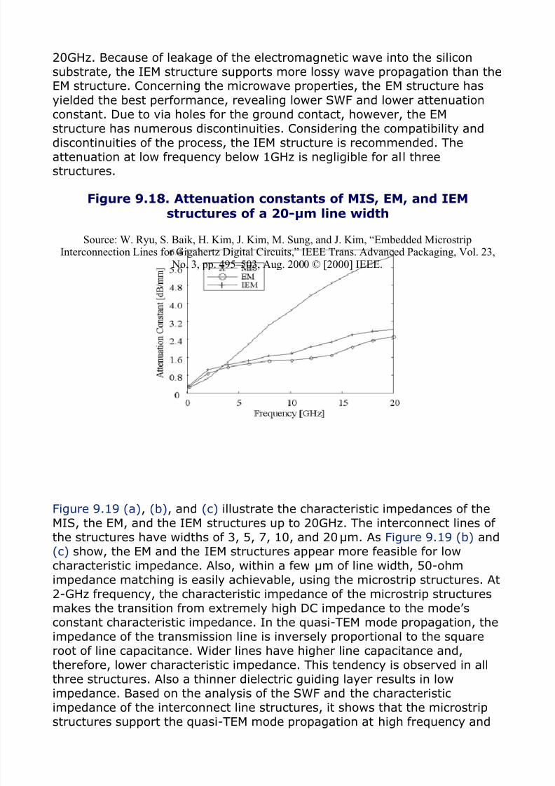
8/10/2019 eetop.cn_Power Integrity for IO Interfaces.pdf
http://slidepdf.com/reader/full/eetopcnpower-integrity-for-io-interfacespdf 390/439
20GHz. Because of leakage of the electromagnetic wave into the siliconsubstrate, the IEM structure supports more lossy wave propagation than theEM structure. Concerning the microwave properties, the EM structure has
yielded the best performance, revealing lower SWF and lower attenuationconstant. Due to via holes for the ground contact, however, the EMstructure has numerous discontinuities. Considering the compatibility anddiscontinuities of the process, the IEM structure is recommended. Theattenuation at low frequency below 1GHz is negligible for all threestructures.
Figure 9.18. Attenuation constants of MIS, EM, and IEMstructures of a 20-μm line width
Source: W. Ryu, S. Baik, H. Kim, J. Kim, M. Sung, and J. Kim, “Embedded MicrostripInterconnection Lines for Gigahertz Digital Circuits,” IEEE Trans. Advanced Packaging, Vol. 23,
No. 3, pp. 495–503, Aug. 2000 © [2000] IEEE.
Figure 9.19 (a), (b), and (c) illustrate the characteristic impedances of theMIS, the EM, and the IEM structures up to 20GHz. The interconnect lines ofthe structures have widths of 3, 5, 7, 10, and 20μm. As Figure 9.19 (b) and
(c) show, the EM and the IEM structures appear more feasible for lowcharacteristic impedance. Also, within a few μm of line width, 50-ohmimpedance matching is easily achievable, using the microstrip structures. At2-GHz frequency, the characteristic impedance of the microstrip structuresmakes the transition from extremely high DC impedance to the mode’sconstant characteristic impedance. In the quasi-TEM mode propagation, theimpedance of the transmission line is inversely proportional to the squareroot of line capacitance. Wider lines have higher line capacitance and,therefore, lower characteristic impedance. This tendency is observed in allthree structures. Also a thinner dielectric guiding layer results in low
impedance. Based on the analysis of the SWF and the characteristicimpedance of the interconnect line structures, it shows that the microstripstructures support the quasi-TEM mode propagation at high frequency and

8/10/2019 eetop.cn_Power Integrity for IO Interfaces.pdf
http://slidepdf.com/reader/full/eetopcnpower-integrity-for-io-interfacespdf 391/439
are more appropriate to achieve 50-ohm impedance.
Figure 9.19. Characteristic impedance of MIS, EM, and IEMstructures depending on the line widths of 3, 5, 7, 10, 20μm. (All
data is extracted from de-embedded S-parameters.) (a)characteristic impedance of MIS structure. (b) characteristic
impedance of EM structure. and (c) characteristic impedance ofIEM structure.
Source: W. Ryu, S. Baik, H. Kim, J. Kim, M. Sung, and J. Kim, “Embedded MicrostripInterconnection Lines for Gigahertz Digital Circuits,” IEEE Trans. Advanced Packaging, Vol. 23,
No. 3, pp 495–503, Aug. 2000 © [2000] IEEE.
[View full size image]
To provide high-performance interconnect line structures for GHz ICs andSoCs, transmission line structures, such as the EM and the IEM structures,are required. These two structures exhibit constant impedance and high-phase velocities at frequencies more than 1GHz. Due to the high dielectricloss of the substrate, we found that the conventional MIS structure couldnot support the quasi-TEM mode propagation. On the other hand, it isproved that the transmission line structures, including EM and IEM, cancarry GHz digital signals with the quasi-TEM mode.
9.1.4.3. On-Chip PDN Characterization
The performance of the on-chip PDN can be measured by on-wafer VNA

8/10/2019 eetop.cn_Power Integrity for IO Interfaces.pdf
http://slidepdf.com/reader/full/eetopcnpower-integrity-for-io-interfacespdf 392/439
characterization. As discussed in Chapter 4, “System Interconnects,”different elements of on-chip PDN exist, which include power grid,intentional decoupling capacitors, and unintentional decoupling capacitors.
For determining the power grid parasitics, a special test vehicle needs to bedesigned, containing only the power grid, as shown in Figure 5.30. Thereare two structures on this vehicle: open power grid and short power grid.Because no access exists to probe the die at the lower metal layers, thesetwo structures are needed. With measuring both the open and short S-parameters of the grid, the [2×2] matrix can be constructed and the simple
RLGC model can be extracted.
For the on-chip PDN of the entire interface, the S-parameters are probed onthe wafer. Figure 5.36 shows the on-chip PDN measurements for the I/Ointerface. This measurement can verify the on-chip model, constructed withgrid and intentional/unintentional capacitors. Note that for the on-chip
interface, the measurements can be performed on the die-bumps, usingsmall VNA probes. If the bump size is too small compared to the probe size,the two probes in the two-port method may connect to different sets ofpower/ground bumps. In that case, the die-bumps for the two ports need tobe electrically close. If higher parasitics exist between two power bumps,due to on-chip routing, then two-port method cannot be used to acquire theZ
11 of the on-chip PDN; however, Z
21, the transfer impedance between two
bumps, can be obtained.
9.1.5. Pad Capacitance Characterization
The I/O device pad capacitance (Cpad
) consists of all the capacitance seen
from the chip pad; this may include capacitance of I/O circuits andinterconnects. It can be measured by VNA in the frequency domain. Thedevice capacitance can be extracted from the measured S-parameters.
9.1.5.1. Lower- and Upper-Frequency Limit
Due to large amount of reflection, VNA measurement and extraction error
increases significantly. Thus, we need to select frequency range of Cpad extraction properly so the errors can be minimized. We define a dynamicrange indicator (DRI) for reflection loss, due to C
pad, based on the following
equation:
Equation 9.21
where ZCpad
is the impedance of the I/O capacitance Cpad
. As frequency

8/10/2019 eetop.cn_Power Integrity for IO Interfaces.pdf
http://slidepdf.com/reader/full/eetopcnpower-integrity-for-io-interfacespdf 393/439
decreases, impedance of the Cpad increases and the DRI decreases, makingthe measurement more difficult and increasing the extraction error. Table9.1 shows with different Cpad value, how DRI varies with frequency change.
In most instances, the expected Cpad value is under 2pF. Therecommended DRI for a Cpad measurement is 40dB or lower. For example,the magnitude of impedance for Cpad = 1pF at 20MHz is approximately8kΩ. Assuming a VNA with a 50Ω reference impedance, its DRI equals to38dB. Cpad of 1pF can be measured from 20MHz up to the first resonancefrequency. Open-circuited transmission line has resonant frequency at one-
quarter wavelength (λ /4). At the frequency of one-quarter wavelength ofthe interconnects, the dynamic range clearly decreases. The higher end ofthe frequency range for Cpad extraction should be conducted << λ /4frequency. Longer package and PCB interconnect lines have lower resonantfrequency. The parasitic inductance effect (3D electromagnetic effect) andreturn path effect will further decrease the resonance frequency.
9.1.5.2. De-Embedding Method
A number of various approaches have been developed for removing theeffects of the test fixture from the measurement. These approaches fall intotwo fundamental categories: Direct measurement and de-embedding. De-embedding uses a model of the test fixture and mathematically removes thefixture characteristics from the overall measurement.
This fixture de-embedding procedure can produce extremely accurate
results for the noncoaxial DUT, without complex noncoaxial calibrationstandards. For this case, the de-embedded measurements can be post-processed from the measurements made on the test fixture and DUT
Table 9.1. VNA DRI of Cpad MeasurementVersus Frequency
Cpad Frequency DRI (dB)
1pF 1MHz 64
10MHz 44
20MHz 38
2pF 1MHz 58
10MHz 38
20MHz 32
3pF 1MHz 54.5
5MHz 40.5
10MHz 34.6

8/10/2019 eetop.cn_Power Integrity for IO Interfaces.pdf
http://slidepdf.com/reader/full/eetopcnpower-integrity-for-io-interfacespdf 394/439
together. Using a different calibration model, we can also perform the de-embedding calculation directly on the VNA.
In the single-ended two-port based de-embedding, as Figure 9.20 shows,we use the test setup #2 to obtain the [2×2] S parameter of bare packageand use test setup #1 to get the S
11
of the package with die.
Figure 9.20. Block diagram of single-ended two-Port de-embedding method
The de-embedding formulae are listed here:

8/10/2019 eetop.cn_Power Integrity for IO Interfaces.pdf
http://slidepdf.com/reader/full/eetopcnpower-integrity-for-io-interfacespdf 395/439
Equation 9.22
Equation 9.23
Equation 9.24
where S11_dev
and Z11_dev are return loss and input impedance of I/O
device and f is frequency. S11
, S12
, S21
, and S22
are two-port S-parameter
of test fixtures, including bare package and PCB, as shown in Figure 9.20.
9.1.6. Power Delivery-to-Signal Coupling
Measurement
Jongbae Park et al. [22] experimentally demonstrated the SimultaneouslySwitching Output (SSO) noise coupling effect to signal. In his experimentalstudy, the DUT has 190mm X 80mm size and the six-layer stack up same tothat of DDR memory module as shown in Figure 9.21. DUTs have fourdifferent signal line structures, a ground referenced microstrip line (Type-1), a ground referenced strip line (Type-2), a power referenced strip line(Type-3), and a power referenced microstrip line (Type-4), as shown inFigure 9.22. Total line length is 80mm and line length between vias is60mm. The clock driver chip was implemented as an SSO source.
Figure 9.21. Top view of test DUTs [22]
Source: J. Park, et al, “Noise coupling to signal trace and via from power/ground simultaneousswitching noise in high speed double data rates memory module,” Proceeding of EMC 2004 ©
[2004] IEEE.

8/10/2019 eetop.cn_Power Integrity for IO Interfaces.pdf
http://slidepdf.com/reader/full/eetopcnpower-integrity-for-io-interfacespdf 396/439
Figure 9.22. Cross-section of manufactured DUTs, which have asix -layer stackup that is the same to that of the DDR memorymodule. DUTs have different signal line structure: (a) ground
referenced microstrip line (Type-1), (b) ground referenced stripline (Type-2), (c) power referenced strip line (Type-3), and (d)
power referenced microstrip line (Type-4). [22]
Source: J. Park, et al, “Noise coupling to signal trace and via from power/ground simultaneousswitching noise in high speed double data rates memory module,” Proceeding of EMC 2004 ©
[2004] IEEE.
[View full size image]

8/10/2019 eetop.cn_Power Integrity for IO Interfaces.pdf
http://slidepdf.com/reader/full/eetopcnpower-integrity-for-io-interfacespdf 397/439
Figure 9.23 shows the measured coupling ratio, ‘S21
’, to evaluate the SSO
coupling effect to the signal. Port1 is placed between the power and groundplane at the center of the clock driver chip, and port2 is located at the oneend of the signal trace, of which the other end is terminated by 50Ohm. Asshown in Chapter 7, “Signal/Power Integrity Interactions,” there are two
SSO coupling mechanisms. The first SSO coupling mechanism is throughthe reference changing via, and the second coupling mechanism is SSOcoupling to signal through the trace between power and ground plane.Because of the first SSO coupling mechanism, the amount of the SSOcoupling to the power referenced signal line structure with the referencechanging vias is larger than that to the ground referenced signal line
structure without the reference changing vias. It is also shown that becauseof the second SSO coupling mechanism, the amount of the SSO coupling tothe stripline is larger than that to the microstrip line. Through the frequencydomain measurement result, we can confirm that the reference changingvia is the dominant factor to couple the SSO. The peak of coupling
coefficient corresponds to either the plane resonant or signal resonantmode. The plane-to-signal coupling significantly increases at resonance.
Figure 9.23. Measured coupling ratio, S21
, to evaluate the
coupling of power/ground noise to the signal trace. Port1 isplaced between power and ground plane at the center of SSO
generating chip, and port2 is located at the one end of the signaltrace, which the other end is terminated by 50Ohm. Ground
referenced microstrip line (dotted line), ground referenced stripline (dash-dotted line), power referenced strip line (dashedline), and power referenced microstrip line (solid line) [22].
Source: J. Park, et al, “Noise coupling to signal trace and via from power/ground simultaneousswitching noise in high speed double data rates memory module,” Proceeding of EMC 2004 ©
[2004] IEEE.
[View full size image]

8/10/2019 eetop.cn_Power Integrity for IO Interfaces.pdf
http://slidepdf.com/reader/full/eetopcnpower-integrity-for-io-interfacespdf 398/439

8/10/2019 eetop.cn_Power Integrity for IO Interfaces.pdf
http://slidepdf.com/reader/full/eetopcnpower-integrity-for-io-interfacespdf 399/439
No part of any chapter or book may be reproduced or transmitted in any form by any means withoutthe prior written permission for reprints and excerpts from the publisher of the book or chapter.Redistribution or other use that violates the fair use privilege under U.S. copyright laws (see 17USC107) or that otherwise violates these Terms of Service is strictly prohibited. Violators will be
prosecuted to the full extent of U.S. Federal and Massachusetts laws.
9.2. Equivalent Circuit Model Extraction
9.2.1. Need for an Equivalent Circuit Model
Measured frequency domain data provides useful behavioral information of
the DUT. However, it is often required to extract circuit parameters from themeasured data: (1) to validate whether the DUT meets the specificationrequirements and (2) to provide necessary circuit information forsimulations. Especially, as some on-chip parameters are relatively sensitivecompared with other off-chip parameters and their contribution to thesystem simulation proves substantial. Therefore, it is crucial to obtain
precise measurement and accurate extraction algorithm and methodology.
9.2.1.1. Validation Purpose
In the design of an electrical system, specification of a device is assumed tobe within a certain tolerance. However, because of manufacturingtolerances and faults, the specifications are often broken. To validate theDUT, frequency domain S-parameter measurement on the device isperformed. Nevertheless, because the measured data is in the frequency
domain, it is difficult to judge if the S-parameter data has passed thepass/fail criteria. Therefore, the extraction of parameters using predefinedtopology is required to validate the device. Figure 9.24 shows an example of one-port S-parameter data and its approximated circuit topology. It alsoshows a signal line terminal at the package BGA location. From the
measured and simulated S-parameters, it is required to fit them in thegiven equivalent circuit topology. It is required to extract the criticalparameters, such as C
pad and R
term from the measured S-parameter.
Figure 9.24. Example of equivalent topology for package andtransistor pad

8/10/2019 eetop.cn_Power Integrity for IO Interfaces.pdf
http://slidepdf.com/reader/full/eetopcnpower-integrity-for-io-interfacespdf 400/439
9.2.1.2. Simulation Purpose
Simulation of measured S-parameter data can be easily conducted usingthe S-parameter import capability in the most SPICE-compatible simulator.
However, doing so provides a probing point only at the ports of themeasurement. To probe the signal on the inside of the DUT, the extractionof circuit parameters, as shown in Figure 9.24, should be accurately done.
9.2.2. Extraction Methodology
The extraction of the parameters from the frequency domain measurementdata requires knowledge on computational numerical analysis and systemfunction. Figure 9.24 shows a Z-parameter calculation of a DUT topology.
Equation 9.25
Equation 9.26
where s is jω.

8/10/2019 eetop.cn_Power Integrity for IO Interfaces.pdf
http://slidepdf.com/reader/full/eetopcnpower-integrity-for-io-interfacespdf 401/439
There are five unknown variables: C1, L
1, R
3, C
2, and R
2. Determining
these five variables to minimize the difference with measured Z-parameterleads to an optimization problem or a curve fitting problem. The number ofmeasured data frequency sampled points is higher than the number ofunknown variables. As an over-determined system, it leads to solving a
nonlinear least-square problem. Generalizing the problem statement:Function g of equation (9.27), which constitutes the objective function,needs to be minimized for all frequencies. Equation (9.28) states theoptimization problem for the defined function.
Equation 9.27
Equation 9.28
Here, x depicts a set of unknown variables, f is the frequency, Zmeas
is the
measured Z-parameter, and g is the objective function.
To emphasize certain bandwidth for better fitting, the weight function can
also be used. The modified function should look like equation (9.29), andthe weight function W(f) should have value in between 0 and 1 at eachfrequency point.
Equation 9.29
In summary, the final problem statement becomes a constrained, weighted
nonlinear least-square problem. A number of algorithms and numericalanalysis tools exist to solve the optimization problem.
9.2.2.1. Numerical Error
The extraction of the parameters, using a nonlinear least square solution,
inherently introduces numerical errors because of underflow, overflow, orcancellation. For example, because of the limited floating point accuracy incomputation, the vastly different circuit element units tend to cause errors.Examples of these include pF range capacitors and high-impedance resistors
in the process of a circuit topology transfer function calculation. Theseerrors, due to needless underflow, overflow, or cancellation, can be partially
mitigated by using higher precision algorithms; however, it cannot be a

8/10/2019 eetop.cn_Power Integrity for IO Interfaces.pdf
http://slidepdf.com/reader/full/eetopcnpower-integrity-for-io-interfacespdf 402/439
complete solution. Rescaling, nevertheless, can prevent these errors. It iscrucial to rescale the component values to somewhat similar ranges. Theunknown variable x –{x
0 F, x
1 ohm, x
2 H}, for example, can be rescaled to
{x0 pF, x
1 mohm, x
2 nH} if they are expected to be in pF, mohm, and nH
range, respectively.
9.2.3. Extraction Examples
The following section gives examples of extraction for the signal net and for
the power net.
9.2.3.1. Receiver Model for SI
The signal net I/O interconnection, connected to receiver buffer, shows itsdistinctive characteristics with small inductance, losses in its transmissionline, and small receiver-end capacitance. The topology should be carefullyselected to reflect the I/O signal’s distinctive characteristics. Also, the units
for the unknown variables should be carefully rescaled to avoid any bigaccuracy loss due to numerical errors. Figure 9.25, Figure 9.26, and Figure9.27 show examples of the parameter extraction results, with theaforementioned optimization technique for a structure similar to Figure9.24.
Figure 9.25. Magnitude comparison of extracted versus
measured data
Figure 9.26. Real part comparison of extracted versus measureddata

8/10/2019 eetop.cn_Power Integrity for IO Interfaces.pdf
http://slidepdf.com/reader/full/eetopcnpower-integrity-for-io-interfacespdf 403/439
Figure 9.27. Imaginary part comparison of extracted versusmeasured data
9.2.3.2. PDN Model
All the extraction procedures and algorithms for power net are identical as
those for signal net. Equivalent circuit topology for power net may evenprimarily resemble a topology similar to the signal net. However, thecomponents of the topology often have a different value range than the

8/10/2019 eetop.cn_Power Integrity for IO Interfaces.pdf
http://slidepdf.com/reader/full/eetopcnpower-integrity-for-io-interfacespdf 404/439
signal interconnection components. Rescaling the unknown variablesaccording to the each variable value range is important in obtainingreasonable and accurate solutions. Figure 5.29 shows an example of the
parameter extraction results with the aforementioned optimizationtechnique. In Figure 5.29, the on-chip PDN parameters are extracted whenprobing is done on the package BGA location. The topology of extractedcircuit is shown in Figure 5.27 with on-chip PDN components. Figure 5.31 shows another example of the power net. The response of extracted circuitsand that of the S-parameters correlate well as shown in Figure 5.32.
9.2.3.3. Topology Identification
To represent all the parasitic effects, topology of the inside of the DUTshould be determined based on the configuration at its best. Because of theefficiency limitation of the nonlinear least square solver, the number of
unknown variables should not be too high. Also to make the solution asunique as possible, the ambiguous definition of topology, such as tworesistors R1 and R4 in the same branch as shown in Figure 9.28, should beavoided. Practically, the number of the unknown variable should be keptsmaller than approximately a dozen for one-port measurement data.
Figure 9.28. Example of ambiguous construction of equivalentcircuit topology
9.2.4. Extension to Multiport Measurement
For the multiport S-parameters measurement data, the objective functionshould be modified to accommodate the multiport S-parameters. So theobjective function becomes:
Equation 9.30
Increasing the number of measurement ports increases accuracy of

8/10/2019 eetop.cn_Power Integrity for IO Interfaces.pdf
http://slidepdf.com/reader/full/eetopcnpower-integrity-for-io-interfacespdf 405/439
optimization. However, the cost and physical difficulties of probing inside ofthe DUT often hinder multiport measurement of the devices.

8/10/2019 eetop.cn_Power Integrity for IO Interfaces.pdf
http://slidepdf.com/reader/full/eetopcnpower-integrity-for-io-interfacespdf 406/439
No part of any chapter or book may be reproduced or transmitted in any form by any means withoutthe prior written permission for reprints and excerpts from the publisher of the book or chapter.Redistribution or other use that violates the fair use privilege under U.S. copyright laws (see 17USC107) or that otherwise violates these Terms of Service is strictly prohibited. Violators will be
prosecuted to the full extent of U.S. Federal and Massachusetts laws.
9.3. Time Domain Characterization
The time domain measurement has historically been the standardmeasurement tool for characterizing and troubleshooting I/O signaling andserves as a common method in the areas of signal/power integrity.Oscilloscopes are used for time domain noise and timing measurements.
TDR and TDT are time domain techniques based on the principle of wavereflections and transmissions respectively. The following section addressesthe TDR application with faster rise times.
9.3.1. Time Domain Reflectometry (TDR)
As TDR serves as an extremely effective tool for interconnectioncharacterization and analysis and has been used for the analysis of traceson dielectric substrates of packages and PCBs. The analysis is typically
performed by measuring characteristic impedances or by observing signalprofile to detect failure mechanisms of various transmission lines. Inaddition, some extended applications of TDR on interconnects (transmissionchannels containing connectors and via structures) show impedancevariations as a function of time. This may be a particularly useful tool forthe high-speed interconnect design and validation. However, when it comesto package design and validation, the resolution of conventional TDR is not
sufficient to analyze vertical via effects in multilayer chip-carrier packageswhose thicknesses are about 1mm. This proves especially true when thepackage design validation is performed as standalone, that is, without
assembly of the package on an evaluation PCB.
To increase the resolution, the rise time needs to be decreased; however,this requires hardware reconfiguration in both the incident pulse generatorand the sampling head of the reflected signal, which can be costly. Anotheroption would be a software enhancement using normalization or acalibration algorithm to compensate for the loss due to cables and fixtures.However, this method is available only in certain TDR equipment andreveals limitation due to the fact that it boosts not only the signal level butalso the noise level of the system. It was found that the special type of TDRequipment with a normalization scheme can make about 20–25ps risingtime depending on microprobe pitch, when the ground-signal-ground (GSG)

8/10/2019 eetop.cn_Power Integrity for IO Interfaces.pdf
http://slidepdf.com/reader/full/eetopcnpower-integrity-for-io-interfacespdf 407/439
configurations were used in the measurement setup.
A state of the art TDR with a rise time of 9ps was employed in thecharacterization of multilayer BGA/LGA packages, and its time waveformswere converted into frequency domain to validate its equivalentperformance to 50GHz VNA [16]. Special hardware was used to reduce a
standard TDR rise time of 20–40ps to 9ps. As for the sampling unit, a70GHz bandwidth plug-in was used. It should be mentioned that the directoutput waveform of 9ps module contains too much aberration and could notbe directly applied to the DUT as-is. TDR equipment supports externalsingle channel normalization that uses short and load calibration standardsto remove systematic errors and provides sufficient accuracy in most cases.However, it does not support external dual-channel normalization that maybe either a common or differential normalization. Here, only a single-channel time domain Short, Open, and Load (SOL) calibration algorithm [1]
and single-port S-parameter computation software have been utilized. Thecalibrated step pulse resulting from the aforementioned algorithm provided4-5 times higher resolution reflected signals than conventional TDR. Theincreased resolution clearly indicates the causes of multilayer package’ssignal integrity problems due to vias and planes, which cannot be observedwith a conventional TDR.
9.3.1.1. Development of 9ps TDR Measurement Setup
Figure 9.29 shows 9ps TDR setup and probing solutions. As in VNA, the
time domain TDR/TDT needs to be calibrated before actual DUTmeasurements to reduce systematical errors and uncertainties, due tofixtures and cables. The calibration of 9ps TDR has been computed in twoways: 1) direct convolution and 2) using SOL calibration. The directconvolution is done using
Equation 9.31
where Vtdr
, Vshort
and Vload
are frequency domain data transformed from
TDR reflected, short, and load standards’ waveforms. Note that withsubtracting the load waveform, a port calibration is accomplished. This isthe simplified version of normalization without the digital filter and also thesimplified version of a full one-port calibration when the source impedancematching term is zero. Another calibration is employed using the well-known calibration procedure for VNA, including the source impedancematching error term, and it is expected to provide better accuracy than the
direct convolution method. Among the various calibration methods, we usedSOL as our first attempt. Using the one port error model [16], we can

8/10/2019 eetop.cn_Power Integrity for IO Interfaces.pdf
http://slidepdf.com/reader/full/eetopcnpower-integrity-for-io-interfacespdf 408/439
calculate S11
as
Equation 9.32
Figure 9.29. 9ps TDR/T microprobing setup
Source: D.-H. Han, M. J. Choi, S. Gardiner, B.-S. Xu, J. He, and C. Lee, “Realization of ultra-wideband high-resolution TDR for chip-carrier packages,” Ipack2005-73291, Proceedings of Ipack
2005 © [2005] ASME.
Where the three error terms ED, E
R and E
S can be solved from following
equation
Equation 9.33
where Vshort
, Vload
, and Vopen
denote a short, load and open measured
waveforms, Sshort
, Sload
, and Sopen
are the S11
parameters for short, load
and open standards.
The S-parameters of the calibration standards are assumed to be ideal,

8/10/2019 eetop.cn_Power Integrity for IO Interfaces.pdf
http://slidepdf.com/reader/full/eetopcnpower-integrity-for-io-interfacespdf 409/439
resulting in , and , respectively.
To calculate DFT of the sampled waveforms, the following equation is used
[16]:
Equation 9.34
Where Δt is the sampling interval, vN-1
is the last data value in the N-point
equidistant time samples, and FFTN(k) denotes a N-point FFT calculation on
this series. The frequency resolution is thus , which is in the GHz rangefor a typical sample length and sample rate. The DFT method given hereactually specifies an estimate for the sample value outside of the timewindow to be equal to the last sample. Therefore, it requires that thesample time is long enough to reach a steady state.
9.3.1.2. Package Validation Using TDR
Typical design validation has been done using an evaluation PCB where adesigned package is assembled. The measurements may be completed fromthe topside of the package to the short section of PCB trace escaped from
the bottom of the package in terms of either TDR/TDT or S-parameters.Figure 9.30 shows a typical package stackup for a chip-carrier. Any signalpath consists of a horizontal transmission line, typically located on a surfacelayer, and a vertical via transition whose physical length is less than 1mm.Signal integrity issues primarily arise due to the vertical via transitionsconsisting of long PTH vias, micro vias, and multilayers of conductors. Todemonstrate this, 9ps TDR measurements were made for 50ohm and70ohm microstrip lines and six vertical via transitions from the surface tobottom. Figure 9.31 shows the surface layer where two microstrip lines of58um and 26um widths and six vertical IO signal probing pads are placed.
Figure 9.32 is the collection of each layer snap-shot taken below the corelayer. From the surface layer to the bottom core layer, all the antipaddesigns are identical. The signal channels 1 through 3 also identically differfrom channel 4 through 6 in terms of antipad size. The different antipaddesigns result in different parasitic capacitance values exiting betweensignal paths and crossing planes.
Figure 9.30. A chip-carrier flip chip package
Source: D.-H. Han, M. J. Choi, S. Gardiner, B.-S. Xu, J. He, and C. Lee, “Realization of ultra-
wideband high-resolution TDR for chip-carrier packages,” Ipack2005-73291, Proceedings of Ipack2005 © [2005] ASME.
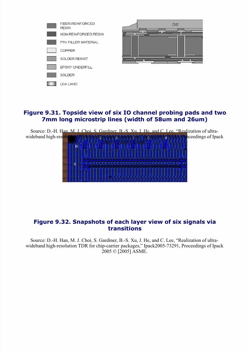
8/10/2019 eetop.cn_Power Integrity for IO Interfaces.pdf
http://slidepdf.com/reader/full/eetopcnpower-integrity-for-io-interfacespdf 410/439
Figure 9.31. Topside view of six IO channel probing pads and two7mm long microstrip lines (width of 58um and 26um)
Source: D.-H. Han, M. J. Choi, S. Gardiner, B.-S. Xu, J. He, and C. Lee, “Realization of ultra-wideband high-resolution TDR for chip-carrier packages,” Ipack2005-73291, Proceedings of Ipack
2005 © [2005] ASME.
Figure 9.32. Snapshots of each layer view of six signals viatransitions
Source: D.-H. Han, M. J. Choi, S. Gardiner, B.-S. Xu, J. He, and C. Lee, “Realization of ultra-
wideband high-resolution TDR for chip-carrier packages,” Ipack2005-73291, Proceedings of Ipack2005 © [2005] ASME.

8/10/2019 eetop.cn_Power Integrity for IO Interfaces.pdf
http://slidepdf.com/reader/full/eetopcnpower-integrity-for-io-interfacespdf 411/439
Figure 9.33 shows 9ps TDR waveforms for a 50ohm microstrip line and68ohm microstrip line with other six vertical IO channels. If the sourceimpedance is 50ohms and traces are routed with 58um microstrip lines,there would be no impedance mismatching on the surface layer. It is alsointeresting to observe that the microstrip impedance profiles are flat about60ps duration, even though the trace length is 7mm long. Due to fastrising-time, open-end waveform does not impact much on the DUT, even ifthe DUT length is not long enough. On the other hand, due to open-end, fora shorter length DUT, a conventional TDR with a 30ps rising time wouldshow increasing slope. It is not difficult to say that microstrip line
impedance characterization structures do not need to be longer than 3-4mm (propagation time of 4*Tr) if 9ps TDR is used to measure theircharacteristic impedances. As may be expected, signals denoted aschannels 1–3 show almost the same impedance waveforms, but they clearlydiffer from channel 4–6 waveforms. Obviously, the larger antipads removealmost all the parasitic capacitances existing below core layers; resulting inbetter impedance matching. The signals denoted as channel 4–6 sufferimpedance mismatching, due to two capacitances separating each other bya PTH inductance. The PTH impedance does not show any severeimpedance mismatching; which means a thick core is not a bottleneck for
high-speed IO signal path. From this study, it becomes clear that the rootcauses of impedance mismatching along the vertical via transition is due toparasitic capacitance that can be reduced by increasing the size of antipadsor the distance between the signal and plane around the antipads. In thisstudy, the antipad size has been increased. Note that the second dip (belowthe core) is larger in magnitude and wider than the first one indicating it ismore capacitive. This indicates there is an additional parasitic capacitanceafter the PTH, and this might be caused by a geometrical mismatching froma micro-via to a large landing pad in the signal path itself.
Figure 9.33. 9ps TDR measurements of six IO signals and twomicrostrip lines

8/10/2019 eetop.cn_Power Integrity for IO Interfaces.pdf
http://slidepdf.com/reader/full/eetopcnpower-integrity-for-io-interfacespdf 412/439
Source: D. H. Han, M. J. Choi, S. Gardiner, B. S. Xu, J. He, and C. Lee, “Realization of ultra-wideband high-resolution TDR for chip-carrier packages,” Ipack2005-73291, Proceedings of Ipack
2005 © [2005] ASME.
[View full size image]
Figure 9.34 shows impedance waveforms of channel 4 with different rising
times. The first curve is measured with 40ps, second with 11ps, and thirdwith 9ps rising time. With a 40ps TDR signal, the package is seen as onecapacitance; therefore, it is hard to identify PTH parasitic components.However, a 9pS TDR signal is fast enough to identify PTH parasiticcomponents.
Figure 9.34. Impedance profiles using three different risingtimes: 9ps, 11ps (dotted), and 40ps (circles).
Source: D. H. Han, M. J. Choi, S. Gardiner, B. S. Xu, J. He, and C. Lee, “Realization of ultra-
wideband high-resolution TDR for chip-carrier packages,” Ipack2005-73291, Proceedings of Ipack2005 © [2005] ASME.
[View full size image]

8/10/2019 eetop.cn_Power Integrity for IO Interfaces.pdf
http://slidepdf.com/reader/full/eetopcnpower-integrity-for-io-interfacespdf 413/439
Using the developed SOL calibration algorithm, 9ps TDR waveforms weremeasured and transformed into the frequency domain for channel 3reflected signal and calibration standards (open, short, and load). Figure9.35 gives the measured TDR waveforms for channel 3 and accordingly theconverted S
11 data in comparison with VNA measurement up to 50GHz. The
sampling interval was 244.14 fs and the total length was 1ns, whichproduces 4,096 samples. The converted S
11
agrees extremely well with VNA
measurement from DC to 50GHz. The difference between the twoconversion methods is minute and occurs around 20GHz. Figure 9.36 demonstrates the TDR measurement and derived S
11 for another signal
channel (channel 4) which has more capacitive parasitic components alongthe path. The correlation with VNA measurement is good up to 10GHzwhereas the calibration method shows closer agreement with VNA data thandirect convolution.
Figure 9.35. 9ps TDR waveforms of channel 3 and S11
comparisons
Source: D.-H. Han, M. J. Choi, S. Gardiner, B. S. Xu, J. He, and C. Lee, “Realization of ultra-

8/10/2019 eetop.cn_Power Integrity for IO Interfaces.pdf
http://slidepdf.com/reader/full/eetopcnpower-integrity-for-io-interfacespdf 414/439
wideband high-resolution TDR for chip-carrier packages,” Ipack2005-73291, Proceedings of Ipack2005 © [2005] ASME.
Figure 9.36. 9ps TDR waveforms of channel 4 and S11comparisons
Source: D. H. Han, M. J. Choi, S. Gardiner, B. S. Xu, J. He, and C. Lee, “Realization of ultra-wideband high-resolution TDR for chip-carrier packages,” Ipack2005-73291, Proceedings of Ipack2005 © [2005] ASME.

8/10/2019 eetop.cn_Power Integrity for IO Interfaces.pdf
http://slidepdf.com/reader/full/eetopcnpower-integrity-for-io-interfacespdf 415/439
Because the faster TDR instrument is pushing the limit of the signal levelclose to the noise level of the system, several aspects deserve special carein practical TDR measurements. It is desirable to collect the TDR and TDTwaveforms and the short/open/load waveforms at one measurement setupand in short-time because, in general, the sampling scope’s long time
stability is found to be much worse than that of the VNA. The long-timeinstability of the TDR instrument causes voltage drift and time base wanderthat may produce errors, which are difficult to compensate later. The userneeds to balance the horizontal scale with the sample length to allow thebeginning and ending part of the sampled waveform to be settled. It ispreferred to keep the same position and vertical scale while capturing allthe TDR/TDT, the short/open/load/through, waveforms. Adjusting thevertical scale to nearly a full range will obtain the best signal-to-noise ratio.Averaging can help reduce random noise in the vertical scale but excessive
averaging will make the capturing procedure too long to obtain a timingerror accumulated; 256-point averaging is selected as the trade-off in thiswork. Time domain comparison is shown in Figure 9.37 and Figure 9.38 forchannel 3 and channel 4, respectively. The rising edge correlates quite well,whereas some part after the rising edge reveals some differences. Thiscorresponds to the better correlation at a high frequency; compared to thatat the middle frequency of the measured bandwidth, as Figure 9.35 andFigure 9.36 show.
Figure 9.37. 9ps TDR waveforms of channel 4 and S11
comparisons
Source: D.-H. Han, M. J. Choi, S. Gardiner, B. S. Xu, J. He, and C. Lee, “Realization of ultra-wideband high-resolution TDR for chip-carrier packages,” Ipack2005-73291, Proceedings of Ipack
2005 © [2005] ASME.
Figure 9.38. 9ps TDR waveforms of channel 4 and S11comparisons
Source: D.-H. Han, M. J. Choi, S. Gardiner, B. S. Xu, J. He, and C. Lee, “Realization of ultra-wideband high-resolution TDR for chip-carrier packages,” Ipack2005-73291, Proceedings of Ipack
2005 © [2005] ASME.

8/10/2019 eetop.cn_Power Integrity for IO Interfaces.pdf
http://slidepdf.com/reader/full/eetopcnpower-integrity-for-io-interfacespdf 416/439
9.3.1.3. Differential TDR and TDT
Driving the two transmission lines by single-ended signals that are exactlyout-of-phase is called differential driving. Differential signaling links have
been widely used to achieve higher noise immunity for multi-GHz I/Ointerfaces. From even/odd measurements, using a differential TDR/TDTinstrument, we can extract differential and common mode impedance andpropagation delay to describe differential transmission line behavior.
Differential impedance consists of the impedance measured between twoconductors driven differentially, whereas the odd mode impedanceconstitutes the impedance of a single conductor in a differential pair. Theeven mode impedance is the impedance of either conductor when the
differential pair is driven with identical, same-polarity signals. Common
mode impedance is the impedance of the two conductors in a differentialpair, when both conductors are driven with a single common mode signal,relative to ground. The differential impedance is twice the value of the oddmode impedance, and the even mode is twice the common mode value. Ifthe common mode impedance is much lower than the differential
impedance, the common mode rejection will be high. In the case of nocoupling between the lines in the differential pair, both even- and odd-modeimpedances approach the single-ended characteristic impedance of eachline [17].
9.3.2. PDN Noise Measurement
PDN noise is also known as supply noise. As Chapter 6, “Time DomainAnalysis,” discusses, there is a specific design target for the PDN noise atthe chip or die. It is especially difficult to measure the die by itself becauseno physical terminal exists for the measurement. When the on-chip noisetravels to the package or the PCB, it becomes significantly modified. Theremay be capacitors on the package that can filter out the noise at higherfrequencies. Also, there may be unwanted PDN resonances on the package
and PCB, so at the measuring point, the noise may be altered significantly.
PDN noise measurements are performed with an oscilloscope [10], and the

8/10/2019 eetop.cn_Power Integrity for IO Interfaces.pdf
http://slidepdf.com/reader/full/eetopcnpower-integrity-for-io-interfacespdf 417/439
bandwidth of measurement plays an important role. Chapter 5, “FrequencyDomain Analysis,” shows the frequency impact for on-chip PDN, packagePDN, and PCB PDN. The PDN noise measurements may be performed on the
PCB with low bandwidth (~ 20MHz), because the PCB PDN may affect onlythe low frequencies, and the noise coming from the chip may be filtered outbefore it reaches the PCB PDN. If the high-frequency noise is measured onthe PCB, it needs to be properly calibrated, considering the PDN response atthe measurement point of the PCB. For the high frequency PDN noisemeasurement, the bandwidth may be at least three times that of the
maximum clock frequency for the interface. Proper interconnectingelements need to be connected for high-frequency measurements, becausethe parasitics of those elements might skew the results. Power consumptiondue to the PDN needs to be noted, and a DC block might be necessary toprotect the oscilloscope. Many oscilloscopes have FFT functionality, whichmay be used to interpret the frequency contents of the noise. Figure 6.20
shows an example of the FFT display of the waveform.
For the logic and internal circuits, the noise is internal to the chip and notransmission line is involved. The noise travels from chip to package andfrom package to the PCB. Typically, that PDN does not serve as a referenceof the signals. For the final stage of I/O interface, PDN serves as thereference to the signals on the package and on the PCB. Due to resonancesof the PCB PDN, the noise coming from the chip and package may beamplified. In that case, high frequency noise measurement may berequired. In general, the noise measured on the PCB may differ from its
source on the chip, especially at high frequencies. However, high-frequencynoise measurement on the PCB proves helpful in determining unwantedresonance coupling and EMI impacts.
As Chapter 6 discusses, for single-ended or differential interface, the worst-case loading condition is determined. The I/O interface is exercised withthat loading condition. The generated noise at an on-chip power networkneeds to be quantified in the lab. Various ways with which the on-chip oron-die noise can be measured, including the following:
Special on-die circuits: Special on-die circuits like on-die droopdetector as described in [11, 12, 13] are designed to detect the on-dienoise. For designing such circuits, bandwidth of the noise is consideredto be an important parameter. Some types of circuits can detect thepeak noise, and other types can reproduce the time domain waveform.
Picoprobing: Special silicon needs to be fabricated so as to have innermetal on-die points that can be measured with the picoprobe [14].Picoprobes are tiny RF probes that connect to the special silicon so theon-die noise measurements can be completed. In Chapter 6,
picoprobing results were obtained for the SSO type of noisemeasurements, as shown in Figure 6.20. The measurement frequencyis limited by capacitance, so low-capacitance probes need to be used

8/10/2019 eetop.cn_Power Integrity for IO Interfaces.pdf
http://slidepdf.com/reader/full/eetopcnpower-integrity-for-io-interfacespdf 418/439
for high-frequency measurements.
In the fabrication of special silicon, it may or may not be possible toobtain the nearby power and ground terminals. The power terminal andground terminal may be electrically away. This may result in inaccuratemeasurements of the on-die noise. Also, the yield of such samples may
be low, so good quality samples may not be available formeasurements.
On-package measurement: Another alternative is to measure theon-die noise when it travels to the package. In this scenario, specialbumps are designed for the package, and these bumps do not connectto the PCB. These bumps are power and ground bumps for which thenoise needs to be measured.
The measurement is completed on these bumps, and de-embedding isdone from the bump to the buffer to obtain the noise at the power netsof the buffer. Another option is to measure it on the packagedecoupling capacitor location near the chip.
PCB PDN measurements: As mentioned earlier, PDN noise on thePCB may be different than that on the chip itself. However, specialtechniques are used to measure PDN noise on the PCB and to project itat the chip or die. For a single-ended interface, driver side on-chip PDNnoise may be measured at the PCB (receiver). Figure 9.39 shows the
single-ended driver and the terminations at the receiver[15]. The noiseat the power/ground nodes of the driver (point A-C) may be measuredat the receiver. When all the bits at the interface are switching, the on-chip SSO is coupled through the Ron and receiver terminations.
Figure 9.39. Single-ended driver with terminations
Two adjacent DQ bits are used for the measurements: DQH and DQL. The

8/10/2019 eetop.cn_Power Integrity for IO Interfaces.pdf
http://slidepdf.com/reader/full/eetopcnpower-integrity-for-io-interfacespdf 419/439
concept in this instance is that one bit is held high and the other held low.The delta noise at the receiver node D for these two bits is measured. Thisnoise corresponds to the power/ground noise at the driver.
When all other bits are switching simultaneously, it is ensured that the twoDQ bits (DQH and DQL) have identical noise on the power and ground. To
confirm that, both the bits DQH and DQL are held low. When a bit is heldlow, referring to Figure 9.39, the noise at the ground node C of the driverappears at point D. There is some skew in between the DQH and DQL bitswhen both are held low, as shown in Figure 9.40. With this, the waveformsmay be phase-aligned before performing DQH-DQL measurements.
Figure 9.40. Calibration method
Source: V. Pandit, A. N. Pardiwala, Hsiao-ching Chuang, M. J. Choi, and Md. R. Quddus, “SSO Noise, Eye Margin, and Jitter Characterization for I/O Power Integrity,” DesignCon 2009.
[View full size image]
Next, the DQH probe is held high. Referring to Figure 9.39, the noise at thepower node A appears at point D. Now, DQH line is held high and DQL heldlow. Figure 9.41 shows the DQH noise, DQL noise, and the DQH-DQL delta
noise.
Figure 9.41. DQH-DQL measured noise with 1010 data pattern
Source: V. Pandit, A. N. Pardiwala, Hsiao-ching Chuang, M. J. Choi, and Md. R. Quddus, “SSO Noise, Eye Margin, and Jitter Characterization for I/O Power Integrity,” DesignCon 2009.

8/10/2019 eetop.cn_Power Integrity for IO Interfaces.pdf
http://slidepdf.com/reader/full/eetopcnpower-integrity-for-io-interfacespdf 420/439
The switching data lines have a 1010 pattern with maximum MTPS data
rate. The delta noise has a maximum frequency component. This deltanoise is measured at D, so the transfer function from point A to D needs tobe determined. Various components in the system from point A to D exist,like Ron, transmission lines, and connectors. The losses due to these arecalibrated out. Figure 9.42 shows the voltage transfer function in afrequency domain from point A to point D.
Figure 9.42. Transfer function for determining on-chip noise
Source: V. Pandit, A. N. Pardiwala, Hsiao-ching Chuang, M. J. Choi, and Md. R. Quddus, “SSO Noise, Eye Margin, and Jitter Characterization for I/O Power Integrity,” DesignCon 2009.
This transfer function is applied to measured noise at point D, and theprojected noise at the driver (V
A-C) is plotted. Similarly, the process is
repeated for other frequency points. Figure 6.22 in Chapter 6 showsresultant noise from the DQH-DQL method.
This DQH-DQL method is specifically for the driver for the single-endedinterface, as shown in Figure 9.39. For a differential interface, a similarmethod may be used, based on the topology of the driver, as shown in

8/10/2019 eetop.cn_Power Integrity for IO Interfaces.pdf
http://slidepdf.com/reader/full/eetopcnpower-integrity-for-io-interfacespdf 421/439
reference [18].
9.3.3. SSO Coupling Measurement in Time Domain
To characterize the time domain SSO coupling effect of the test vehicle,shown in Figure 9.21 and Figure 9.22, the measurement for clock signalwas done with an oscilloscope and pulse pattern generator. The clock driver
chip consumes about 200mA current with 200MHz frequency and generatesSSO. The SSO is about 600mV and dominant at 400MHz because thesecond harmonic of the frequency consuming the current from the powerand ground plane encounters with the power/ground cavity resonance modeTM(1, 0), which is at 400MHz. Figure 9.43 shows the spectrum of themeasured SSO and the power/ground self impedance at the center of clock
driver chip. The generated SSO is dominant at 400MHz because the secondharmonic of the frequency consuming current from power/ground
encounters with the power/ground cavity resonance mode TM(1, 0), whichis at 400MHz.
Figure 9.43. Spectrum of the measured SSO and the cavityresonance modes power/ground self-impedance at the center of
the SSO generating chip
Source: J. Park, et al, “Noise coupling to signal trace and via from power/ground simultaneousswitching noise in high speed double data rates memory module,” Proceeding of EMC 2004 ©
[2004] IEEE.
A 200-MHz clock with a 500mV peak to peak is used to compare the fourdifferent signal line structures, as shown in Figure 9.21 and Figure 9.22.When no SSO exists, the output clock waveforms for the four different
signal line structures are as shown in Figure 9.44 (a). No difference for linestructures exists. Their spectrums possess odd harmonics for ideal clock,with the half of duty cycle, as shown in Figure 9.44 (b). However, when a

8/10/2019 eetop.cn_Power Integrity for IO Interfaces.pdf
http://slidepdf.com/reader/full/eetopcnpower-integrity-for-io-interfacespdf 422/439
600mV SSO noise exists between power/ground planes, the outputwaveforms for the four different signal line patterns are differentlydistorted, as shown in Figure 9.45 (a). Figure 9.45 (b) shows spectrums to
analyze the cause of distortion. As mentioned earlier, there are two SSOcoupling mechanisms: first through the reference changing via, and thesecond is SSO coupling to signal through the trace between power andground plane. It is shown that the 400MHz element, which is the dominantelement of the SSO, is added on the spectrum of the ideal clock signal.Type-3, which is the power referenced strip line, has the highest 400MHz
element because it is coupled by both the first and second SSO couplingmechanism. Nevertheless, the 400MHz element of Type-4 has almost thesame amount as that of Type-3, due to reference transition, which is thedominant factor to couple the SSO. However, Type-1 and Type-2, withoutreference transition, have little SSO coupling to signal line.
Figure 9.44. Signaling with no SSO noise (a) output clockwaveforms and (b) output clock spectrum of 200MHz input clocksignal with 500 mV peak to peak, when there is no SSO
Source: J. Park, et al, “Noise coupling to signal trace and via from power/ground simultaneousswitching noise in high speed double data rates memory module,” Proceeding of EMC 2004 ©
[2004] IEEE.

8/10/2019 eetop.cn_Power Integrity for IO Interfaces.pdf
http://slidepdf.com/reader/full/eetopcnpower-integrity-for-io-interfacespdf 423/439
Figure 9.45. SSO noise coupling effect (a) output clockwaveforms and (b) output clock spectrum of 200MHz input clock
signal with 500 mV peak to peak, when a 600 mV SSO exists
Source: J. Park, et al, “Noise coupling to signal trace and via from power/ground simultaneousswitching noise in high speed double data rates memory module,” Proceeding of EMC 2004 ©
[2004] IEEE.

8/10/2019 eetop.cn_Power Integrity for IO Interfaces.pdf
http://slidepdf.com/reader/full/eetopcnpower-integrity-for-io-interfacespdf 424/439
As previously mentioned, the power referenced microstrip line and powerreferenced strip line with reference changing via are most sensitive to SSOcoupling. However, to change a reference plane is inevitable to effectively
route many data or command lines in memory module. To mitigate SSOnoise coupling to signal trace, it is recommended to place stitching vias orcapacitors at the position with low power/ground cavity impedance asdescribed in Chapter 7.
9.3.4. Jitter Measurement
Jitter, an important measure, must be modeled accurately in systembudgeting. In measurement, jitter is measured with a real-time
oscilloscope. For a single-ended system, Chapter 6 shows examples of
supply noise induced jitter. For a source synchronous single ended system,there is data DQ and strobe DQS. Measuring individual jitter of DQ or DQS,it is triggered on the system clock for that interface. Although the clock may

8/10/2019 eetop.cn_Power Integrity for IO Interfaces.pdf
http://slidepdf.com/reader/full/eetopcnpower-integrity-for-io-interfacespdf 425/439
have jitter, the overall jitter level of the clock may be lower than that forDQ or DQS. Figure 6.34 shows DQ jitter when triggered on the clock. If thewindow margin is required to be determined, the DQ is triggered on the
DQS. Figure 6.37 shows an example of the DQ jitter when triggered on theDQS.
As Chapter 6 describes, different elements of the total jitter exist, such asrandom and deterministic. For a differential interface, if the separate clockis not sent along with the data, it is a nonsource synchronous interface. Theclock, embedded in the data, has to be recovered at the receiver. Jitterrequirements for such a system are more stringent compared to those forsource-synchronous system. A differential interface is expected to have acertain bit error rate (BER) and can be measured with the BER tester. Eyediagrams can be obtained using an oscilloscope for the differential signals atthe receiver. The relationship between the eye margin and the BER needs to
be established, and different components of the jitter need to bedetermined. More details of the jitter for high-speed links, including thestatistical approach can be found in references [19, 20, 21]. Signal integrityimpact along with power integrity impact on jitter is described in Chapter 8,
“Signal/Power Integrity Co-Analysis.” It illustrates that due to the SSOimpact, there is a nonlinear modulation on the signal pad of thecorresponding victim buffer, which is another source of jitter. As the systembudget gets tighter it is necessary to include jitters from various noisesources such as SSO, ISI, crosstalk, and combinations thereof. Advancedcomputational capability facilitates modeling of these sources and
interactions between them. Measurement of jitter of the active system hasalso been improving with the advancement in the equipment and thecomputational algorithm.

8/10/2019 eetop.cn_Power Integrity for IO Interfaces.pdf
http://slidepdf.com/reader/full/eetopcnpower-integrity-for-io-interfacespdf 426/439
No part of any chapter or book may be reproduced or transmitted in any form by any means withoutthe prior written permission for reprints and excerpts from the publisher of the book or chapter.Redistribution or other use that violates the fair use privilege under U.S. copyright laws (see 17USC107) or that otherwise violates these Terms of Service is strictly prohibited. Violators will be
prosecuted to the full extent of U.S. Federal and Massachusetts laws.
References
1. Robert Schaefer, “Limitations and Accuracies of Time and FrequencyDomain Analysis of Physical Layer Devices,” Agilent’s presentation atDesignCon, 2005.
2. Istvan Novak, “Probes and setup for measuring power-plane impedanceswith vector network analyzer,” DesignCon, 1999.
3. Istvan Novak, “Probes Frequency Domain Power DistributionMeasurements -An Overview,” DesignCon 2003 East, High-PerformanceSystem Design Conference, Boston, MA, June 23–25, 2003.
4. Xu, Minjia, Yun Ji, T. H. Hubing, and T.P. Van Doren, and J.L. Drewniak, “Development of a Closed-form Expression for the Input Impedance of
Power-ground Plane Structures,” IEEE Int. Symp. ElectromagneticCompatibility , Vol. 1, 77–82, 2000.
5. The facts about the impedance of power and ground planes.www.sigrity.com/papers/InputImp/InputImp.htm.
6. H. Hasegawa, M. Furukawa, and H. Yanai, “Properties of microstrip lineson Si-SiO2 system,” IEEE Trans. Microwave Theory Tech., Vol. MTT-19, pp869–881, Nov. 1971.
7. W. Ryu, S. Baik, H. Kim, J. Kim, M. Sung, and J. Kim, “EmbeddedMicrostrip Interconnection Lines for Gigahertz Digital Circuits,” IEEE Trans.Advanced Packaging, Vol. 23, No. 3, pp 495–503, Aug. 2000.
8. Min Wang, Ravindran Mohanavelu, and Woong Hwan Ryu, “An OptimumClocking Design with Frequency-Tabulated W-Element InterconnectModels,” Finalist for Best Paper Award, DesignCon2006, Feb 2006.
9. Y. Eo and W.R. Eisenstadt, “High-Speed VLSI Interconnect ModelingBased on S-parameter Measurements,” IEEE Trans. Comp. Hybrid, Manuf.
Technol., Vol. 16, No. 5, Aug. 1993.
10. Application Note 1592, Tips and Techniques for Making Power Supply

8/10/2019 eetop.cn_Power Integrity for IO Interfaces.pdf
http://slidepdf.com/reader/full/eetopcnpower-integrity-for-io-interfacespdf 427/439
Noise Measurements with an Oscilloscope,http://cp.literature.agilent.com/litweb/pdf/5989-6755EN.pdf .
11. Muhtaroglu, A.; Taylor, G.; Rahal-Arabi, T., “On-die droop detector foranalog sensing of power supply noise,” Solid-State Circuits, IEEE Journal,Volume 39, Issue 4, April 2004 pp 651–660.
12. Sehgal, A.; Song, P.; and Jenkins, K.A., “On-chip Real-Time PowerSupply Noise Detector,” Solid-State Circuits Conference, 2006. ESSCIRC2006. Proceedings of the 32nd European, Sept. 2006 Page(s): 380–383.
13. E. Alon, V. Stojanovic, and M. Horowitz, “Circuits and techniques forhigh-resolution measurement of on-chip power supply noise,” VLSI Circuits,2004. Digest of Technical Papers. 2004 Symposium on, 17–19 June 2004 pp102–105.
14. Laung-Terng Wang, Charles Stroud, and Nur Touba, “System-on-ChipTest Architectures: Nanometer Design for Testability,” Morgan Kaufmann,2007.
15. V. Pandit, A. N. Pardiwala, Hsiao-ching Chuang, M. J. Choi, and Md. R.Quddus, “SSO Noise, Eye Margin, and Jitter Characterization for I/O PowerIntegrity,” DesignCon 2009.
16. Dong-Ho Han, Myoung J Choi, Scott Gardiner, Bao-Shu Xu, Jiangqi He,and Cliff Lee, “Realization of ultra-wideband high-resolution TDR for chip-carrier packages,” Ipack2005-73291, Proceedings of Ipack 2005, AmericanSociety of Mechanical Engineers, July 17–22, 2005, San Francisco, CA.
17. TDA Systems “Characterization of Differential Interconnects from TDRMeasurements” Application Note.
18. Schmitt, R. and Chuck Yuan, “Power supply noise modeling andcorrelation for a 3.2 GHz bidirectional differential memory bus,” ElectricalPerformance of Electronic Packaging, 2004. IEEE 13th Topical Meeting
2004, pp 225– 228.
19. “Signal Integrity Measurement Methods and Practices,” Tutorial Session,DesignCon 2009.
20. M. P. Li, “Jitter And Signaling Test For High-Speed Links,” Conference2006, IEEE Custom Integrated Circuits, 10–13 Sept. 2006, pp. 65–72.
21. M. A. Kossel and M.L. Schmatz, “Jitter measurements of high-speedserial links,” Design & Test of Computers, IEEE, Volume 21, Issue 6, Nov–
Dec 2004, pp 536–543.
22. J. Park, H. Kim, J. S. Pak, Y. Jeong, S. Baek, J. Kim, J. Lee, and J. Lee,

8/10/2019 eetop.cn_Power Integrity for IO Interfaces.pdf
http://slidepdf.com/reader/full/eetopcnpower-integrity-for-io-interfacespdf 428/439
“Noise coupling to signal trace and via from power/ground simultaneousswitching noise in high speed double data rates memory module,”Proceeding of EMC , Vol. 2, pp 592–597, August 2004.

8/10/2019 eetop.cn_Power Integrity for IO Interfaces.pdf
http://slidepdf.com/reader/full/eetopcnpower-integrity-for-io-interfacespdf 429/439

8/10/2019 eetop.cn_Power Integrity for IO Interfaces.pdf
http://slidepdf.com/reader/full/eetopcnpower-integrity-for-io-interfacespdf 430/439

8/10/2019 eetop.cn_Power Integrity for IO Interfaces.pdf
http://slidepdf.com/reader/full/eetopcnpower-integrity-for-io-interfacespdf 431/439

8/10/2019 eetop.cn_Power Integrity for IO Interfaces.pdf
http://slidepdf.com/reader/full/eetopcnpower-integrity-for-io-interfacespdf 432/439

8/10/2019 eetop.cn_Power Integrity for IO Interfaces.pdf
http://slidepdf.com/reader/full/eetopcnpower-integrity-for-io-interfacespdf 433/439

8/10/2019 eetop.cn_Power Integrity for IO Interfaces.pdf
http://slidepdf.com/reader/full/eetopcnpower-integrity-for-io-interfacespdf 434/439

8/10/2019 eetop.cn_Power Integrity for IO Interfaces.pdf
http://slidepdf.com/reader/full/eetopcnpower-integrity-for-io-interfacespdf 435/439

8/10/2019 eetop.cn_Power Integrity for IO Interfaces.pdf
http://slidepdf.com/reader/full/eetopcnpower-integrity-for-io-interfacespdf 436/439

8/10/2019 eetop.cn_Power Integrity for IO Interfaces.pdf
http://slidepdf.com/reader/full/eetopcnpower-integrity-for-io-interfacespdf 437/439

8/10/2019 eetop.cn_Power Integrity for IO Interfaces.pdf
http://slidepdf.com/reader/full/eetopcnpower-integrity-for-io-interfacespdf 438/439

8/10/2019 eetop.cn_Power Integrity for IO Interfaces.pdf
http://slidepdf.com/reader/full/eetopcnpower-integrity-for-io-interfacespdf 439/439