ee6502- microprocessors and … · bring about the features of 8259. ... draw and explain the...
TRANSCRIPT

1
EE6502- MICROPROCESSORS AND MICROCONTROLLERS
UNIT – IV - PERIPHERAL INTERFACING
PART – A
1. What is a Programmable peripheral device?
If the functions performed by a peripheral device can be altered or changed by a program instruction then
the peripheral device is called programmable device. Usually programmable device will have control
registers. The device can be programmed by sending the control word in the prescribed format to the
control register.
2. What are the internal devices of an 8255?
The internal devices of an 8255 are Port A, Port B and Port C. The ports can be programmed for either input
or output function in different operating modes.
3. Bring about the features of 8259. (May/June 2014) (Nov/Dec 2016)
1. It is a programmable interrupt controller. It manages eight interrupt requests. 2. The interrupt vector
addresses are programmable. 3. The priorities of interrupts are programmable. 4. The interrupt can be
masked or unmasked individually.
4. Write a Program to initialize a single 8259 connected to an 8085 processor.
Let us assume that 8259 is IO mapped in the system. The 8259 can be initialized by sending ICW1, ICW2
and OCW1. Let the 8 bit address when A0 = 0 be 00H and when A0 =1 be 01H
MVI A, ICW1 OUT 00 H, MVI A, ICW2 OUT 01H
MVI A, OCW1 OUT 01H
HLT
5. What is the difference in programming master 8259 and slave 8259?
The ICW3 will be different for master 8259 and slave 8259. For master, the ICW3 will inform the IR input
that are having slaves. For slave, the ICW3 will inform its slave ID number.
6. Write the various functional blocks of INTEL 8259.
The various functional blocks of 8259 are Control logic, Read/Write logic, Data bus buffer, Interrupt
Request Register (IRR), Interrupt Mask Register (IMR) and In-Service Register (ISR), Priority Resolver
(PR) and cascade buffer.
7. Name any two types of ADC.
The different types of ADC are successive approximation ADC, Counter type ADC flash type ADC,
integrator converters and voltage to-frequency converters.
8. Why the number of out ports in the peripheral-mapped I/O is restricted to 256 ports?
The number of output ports in the peripheral I/O is restricted to 256 ports because the operand of the OUT
instruction is 8-bits; it can have only 256 combinations
9. Define Memory mapped I/O?
In this method, an I/O device is treated as a memory location. The microprocessor uses 16 - bit address to
identify and I/O device. Thus the memory map is shared between memory and I/O devices.
10. What is an interrupt I/O?
Interrupt is an event that causes the CPU to initiate a fixed sequence known as an interrupt sequence.
11. What are the different ways to end the interrupt execution in 8259 PIC? (May/June 2011) AEOI
(Automatic End of Interrupt) mode the ISR bit is reset at the end of the second INTA pulse. Otherwise, the
ISR bit remains set until the issue of an appropriate EOI command at the end of the interrupt subroutine.
12. What are the different types of DMA?
Cycle stealing (or Single transfer) DMA, Block transfer (or Burst Mode) DMA and Demand transfer DMA.
13. What is Cycle stealing DMA?
In Cycle stealing DMA, the DMA controller will perform one DMA transfer in between instruction cycles
(i.e. in this mode, the execution of one processor instruction and one DMA data transfer will take place
alternatively).
14. What is block and demand transfer mode DMA?
1. In block transfer mode, the DMA controller will transfer a block of data and relieve the bus to processor.
After sometime another block of data is transferred by the DMA and so on.
2. In demand transfer mode, the DMA controller will complete the entire data transfer at a stretch and then
relieve the bus to the processor.
15. What is the function of Scan section in 8279 programmable keyboard/Display controller?
(May/June 2011)(May/June 2016)
2
Scan section which has two modes (i) Encoded Mode (ii) Decoded Mode Encoded Mode: In this mode, Scan counter provides a binary count from 0000 to 1111 the four scan lines
(SC3 – SC0) with active high outputs.
Decoded Mode: The internal decoder decodes the least significant 2 bits of binary count and provides four
possible combinations on the scan lines.
16. What are the output terminals in USART 8251? (May/June 2013)
TXD, TXRDY, TXEMPTY, RXRDY, SYNDET/BD, DTR, RTS.
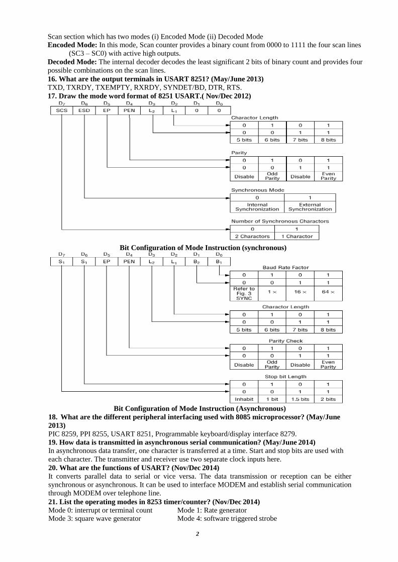
17. Draw the mode word format of 8251 USART.( Nov/Dec 2012)
Bit Configuration of Mode Instruction (synchronous)
Bit Configuration of Mode Instruction (Asynchronous)
18. What are the different peripheral interfacing used with 8085 microprocessor? (May/June
2013)
PIC 8259, PPI 8255, USART 8251, Programmable keyboard/display interface 8279.
19. How data is transmitted in asynchronous serial communication? (May/June 2014)
In asynchronous data transfer, one character is transferred at a time. Start and stop bits are used with
each character. The transmitter and receiver use two separate clock inputs here.
20. What are the functions of USART? (Nov/Dec 2014)
It converts parallel data to serial or vice versa. The data transmission or reception can be either
synchronous or asynchronous. It can be used to interface MODEM and establish serial communication
through MODEM over telephone line.
21. List the operating modes in 8253 timer/counter? (Nov/Dec 2014)
Mode 0: interrupt or terminal count Mode 1: Rate generator Mode 3: square wave generator Mode 4: software triggered strobe

3
Mode 5: hardware triggered strobe
22. What are the internal registers available in 8259 PIC? (May/June 2015)
Interrupt mask register (IMR), Interrupt Request register (IRR) and In-service register (ISR)
23. Distinguish between synchronous and asynchronous transmission. (May/June 2015)
Asynchronous Synchronous
In this, a word or a character is preceded by a start bit and followed by a stop bit.
In this, the transmission begins with a block header, which is a sequence of bits.
Data can be sent one at a time Large amount of data can be transmitted at a time
24. Write the control word value for 8255 PPI when PORT A AND PORT B are inputs in simple
I/O mode. (Nov/Dec 2015,2016)(May/June 2016)
D7 D6 D5 D4 D3 D2 D1 D0
1 0 0 1 X 0 1 X
25. What are the working modes of 8254 timer?(Nov/Dec 2015)
MODE 0: Interrupt on terminal count MODE 1: Hardware retriggerable one-shot
MODE 2: Rate Generator MODE 3: Square Wave Mode
26.What are the internal devices of a typical DAC?(May/June 2016)
It includes R-2R resistor network, an internal latch and current to voltage conversion amplifier.
27. Write a program to find 2’s complement using 8051.(May June 2016)
MOV A,#55,
CPL A
ADD A,01
SJMP

4
UNIT – IV - PERIPHERAL INTERFACING
PART - B
1. Draw and explain the functional block diagram of 8255 PPI.
Data Bus buffer:
• It is a 8-bit bidirectional Data bus.
• Used to interface between 8255 data bus with system bus.
• The internal data bus and Outer pins D0-D7 pins are connected in internally. • The direction of data buffer is decided by Read/Control Logic.
Read/Write Control Logic:
• This is getting the input signals from control bus and Address bus
• Control signal are RD and WR.
• Address signals are A0, A1, and CS.
• 8255 operation is enabled or disabled by CS. Group A and Group B control: • Group A and B get the Control
• Signal from CPU and send the command to the individual control blocks.
• Group A send the control signal to port A and Port C (Upper) PC7-PC4.
• Group B send the control signal to port B and Port C (Lower) PC3-PC0.
• PORT A:
• This is a 8-bit buffered I/O latch.
• It can be programmed by mode 0, mode 1, and mode 2.
• PORT B:
• This is a 8-bit buffer I/O latch.
• It can be programmed by mode 0 and mode 1.
• PORT C:
• This is a 8-bit Unlatched buffer Input and an Output latch.
• It is splitted into two parts. • It can be programmed by bit set/reset operation.
5
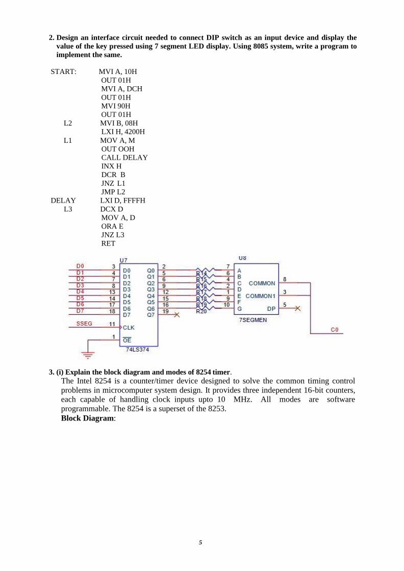
2. Design an interface circuit needed to connect DIP switch as an input device and display the
value of the key pressed using 7 segment LED display. Using 8085 system, write a program to
implement the same.
START: MVI A, 10H
OUT 01H
MVI A, DCH
OUT 01H
MVI 90H
OUT 01H
L2 MVI B, 08H
LXI H, 4200H
L1 MOV A, M
OUT OOH
CALL DELAY
INX H
DCR B
JNZ L1
JMP L2
DELAY LXI D, FFFFH
L3 DCX D
MOV A, D
ORA E
JNZ L3
RET
3. (i) Explain the block diagram and modes of 8254 timer.
The Intel 8254 is a counter/timer device designed to solve the common timing control
problems in microcomputer system design. It provides three independent 16-bit counters, each capable of handling clock inputs upto 10 MHz. All modes are software
programmable. The 8254 is a superset of the 8253.
Block Diagram:

6
Data bus buffer
This 3-state, bi-directional, 8-bit buffer is used to interface the 8254 to the system bus.
Read/write logic
The Read/Write Logic accepts inputs from the system bus and generates control signals
for the other functional blocks of the 8254. A1and A0 select one of the three counters or the Control Word Register to be read from/written into. A ``low'' on the RD input tells the
8254 that the CPU is reading one of the counters. A ``low'' on the WR input tells the 8254 that the CPU is writing either a Control Word or an initial count. Both RD and WR are
qualified by CS, RD and WR are ignored unless the 8254 has been selected by holding CS low. Control word register
The Control Word Register (see Figure 4) is selected by the Read/Write Logic when A1,
A0=11. If the CPU then does a write operation to the 8254, the data is stored in the Control Word Register and is interpreted as a Control Word used to define the operation
of the Counters. The Control Word Register can only be written to; status information is available with the Read-Back Command.
COUNTER 0, COUNTER 1, COUNTER 2 These three functional blocks are identical in operation. The Counters are fully
independent. Each Counter may operate in a different Mode.
MODE 0: INTERRUPT ON TERMINAL COUNT Mode 0 is typically used for event counting. After the Control Word is written, OUT is
initially low, and will remain low until the Counter reaches zero. OUT then goes high and
remains high until a new count or a new Mode 0 Control Word is written into the Counter. GATE=1 enables counting; GATE= 0 disables counting. GATE has no effect on
OUT.
MODE 1: HARDWARE RETRIGGERABLE ONE-SHOT OUT will be initially high. OUT will go low on the CLK pulse following a trigger to begin the one-shot pulse, and will remain low until the Counter reaches zero.
OUT will then go high and remain high until the CLK pulse after the next trigger. After
writing the Control Word and initial count, the Counter is armed.
MODE 2: RATE GENERATOR This Mode functions like a divide-by-N counter. It is typically used to generate a Real
Time Clock interrupt. OUT will initially be high. When the initial count has decremented to 1, OUT goes low for one CLK pulse. OUT then goes high again, the Counter reloads
the initial count and the process is repeated. Mode 2 is periodic; the same sequence is repeated indefinitely.
7
MODE 3: SQUARE WAVE MODE Mode 3 is typically used for Baud rate generation. Mode 3 is similar to Mode 2 except for
the duty cycle of OUT. OUT will initially be high. When half the initial count has expired
OUT goes low for the remainder of the count. Mode 3 is periodic.
MODE 5: HARDWARE TRIGGERED STROBE (RETRIGGERABLE) OUT will initially be high. Counting is triggered by a rising edge of GATE. When the
initial count has expired, OUT will go low for one CLK pulse and then go high again
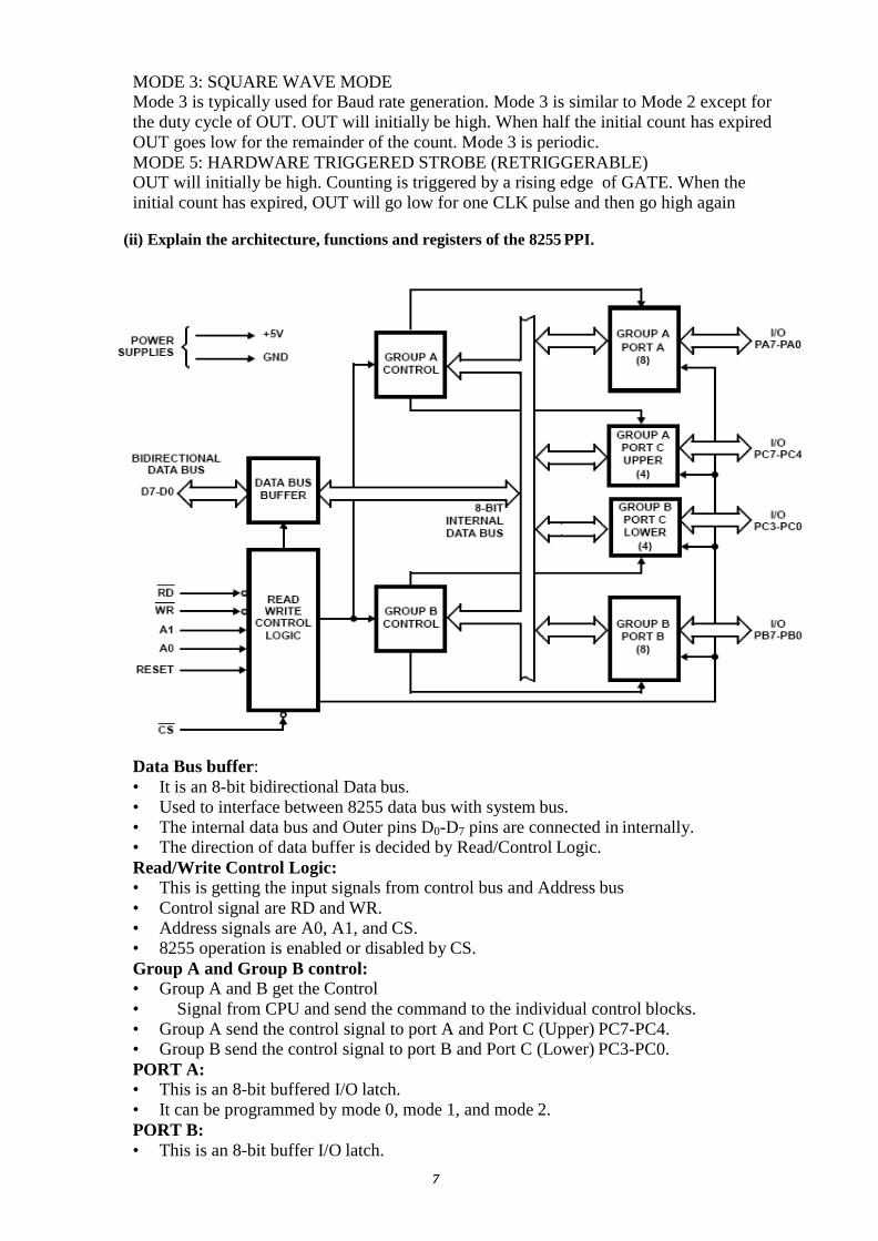
(ii) Explain the architecture, functions and registers of the 8255 PPI.
Data Bus buffer:
• It is an 8-bit bidirectional Data bus.
• Used to interface between 8255 data bus with system bus.
• The internal data bus and Outer pins D0-D7 pins are connected in internally. • The direction of data buffer is decided by Read/Control Logic.
Read/Write Control Logic:
• This is getting the input signals from control bus and Address bus
• Control signal are RD and WR.
• Address signals are A0, A1, and CS. • 8255 operation is enabled or disabled by CS.
Group A and Group B control:
• Group A and B get the Control
• Signal from CPU and send the command to the individual control blocks.
• Group A send the control signal to port A and Port C (Upper) PC7-PC4. • Group B send the control signal to port B and Port C (Lower) PC3-PC0.
PORT A:
• This is an 8-bit buffered I/O latch.
• It can be programmed by mode 0, mode 1, and mode 2.
PORT B:
• This is an 8-bit buffer I/O latch.

8
• It can be programmed by mode 0 and mode 1.
PORT C:
• This is an 8-bit Unlatched buffer Input and an Output latch.
• It is splitted into two parts. • It can be programmed by bit set/reset operation.
4. (i) Write a neat functional block diagram, explain the functions of 8259 PIC.
DATA BUS BUFFER
It is an eight pin bidirectional data bus. Control, Status and Interrupt vector
information are transformed through this bus.
It allows 8259 to send interrupt code and address of interrupt service subroutine to the processor.
READ/WRITE LOGIC
The function of this block is to accept Output commands from the CPU.
It contains the Initialization Command Word (ICW) registers and Operation
Command Word (OCW) registers which store the various control formats for device operation.
This function block also allows the status of the 8259A to be transferred onto the Data Bus.
CONTROL LOGIC
It has two pins: INT as an output which goes high if valid interrupt is asserted.
INTA an acknowledgement from processor to 8259.
CS (CHIP SELECT)
A LOW on this input enables the 8259A. No reading or writing of the chip will occur unless the device is selected.
WR (WRITE)
A LOW on this input enables the CPU to write control words (ICWs and OCWs) to
the 8259A.
RD (READ)
A LOW on this input enables the 8259A to send the status of the Interrupt Request Register (IRR), In Service Register (ISR), the Interrupt Mask Register (IMR), or the Interrupt level onto the Data Bus.
A0
This input signal is used in conjunction with WR and RD signals to write commands into the various command registers, as well as reading the various status registers of
the chip. This line can be tied directly to one of the address lines
9
INTERRUPT REQUEST REGISTER (IRR)
It has 8 input lines (IR0 – IR7) for interrupts. When these lines goes high, the request
are stored in the register.
It registers a request only if the interrupt is unmasked.
IN SERVICE REGISTER (ISR)
ISR keeps track of which interrupts are currently being serviced and the corresponding bit will be set in this register.
PRIORITY RESOLVER
This logic block determines the priorities of the bits set in the IRR. The highest
priority is selected and stored into the corresponding bit of the ISR during INTA
pulse.
INTERRUPT MASK REGISTER (IMR)
The IMR stores the bits which mask the interrupt lines to be masked. The IMR operates on the IRR. Masking of a higher priority input will not affect the interrupt
request lines of lower quality.
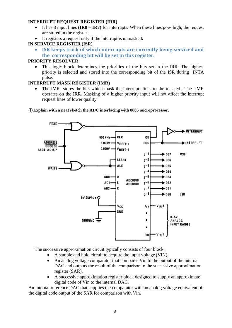
(i) Explain with a neat sketch the ADC interfacing with 8085 microprocessor.
The successive approximation circuit typically consists of four block:
A sample and hold circuit to acquire the input voltage (VIN).
An analog voltage comparator that compares Vin to the output of the internal DAC and outputs the result of the comparison to the successive approximation
register (SAR).
A successive approximation register block designed to supply an approximate
digital code of Vin to the internal DAC.
An internal reference DAC that supplies the comparator with an analog voltage equivalent of
the digital code output of the SAR for comparison with Vin.

10
5. With functional diagram, explain the operation and programming of 8251 USART in detail.
TRANSMITTER
MOV SI, 1500
MOV AL, 36H
OUT 16H, AL
MOV AL, 40H
OUT 10H, AL
MOV AL, 01H
OUT 10H, AL
RELOAD: MOV CL, 05H
CHECK: IN AL, OAH
AND AL, 04H
JZ CHECK
MOV AL, [SI]
OUT 08H, AL
INC SI
11
CMP AL, 3FH
JNZ RELOAD
DEC CL
JNZ CHECK INT 02
RECEIVER: MOV SI, 1500 MOV AL, 36H
OUT 16H, AL MOV AL, 40H
OUT 10H, AL MOV AL, 01H
OUT 10H, AL
RELOAD: MOV CL, 05H
CHECK: IN AL, OAH AND AL, 02H
JZ CHECK IN AL, 08H
MOV [SI], AL INC SI
CMP AL, 3FH JNZ RELOAD
DEC CL JNZ CHECK
INT 02
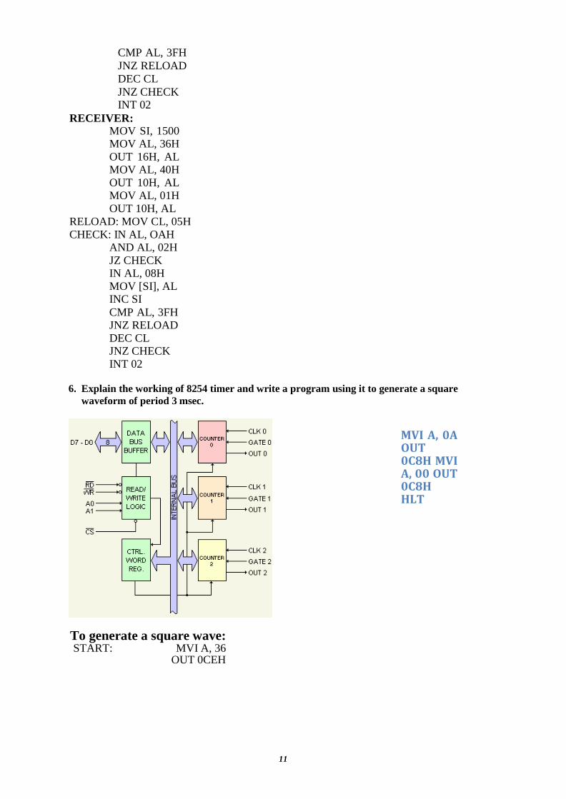
6. Explain the working of 8254 timer and write a program using it to generate a square
waveform of period 3 msec.
To generate a square wave: START: MVI A, 36
OUT 0CEH
MVI A, 0A OUT 0C8H MVI A, 00 OUT 0C8H HLT
12
• A 16 bit count is loaded in its
register and on command, it begins to decrement the count until it reaches 0.At the end of count, it generates a pulse that can be used to interrupt the CPU.
• The counter can count in binary or BCD.
• 6 Modes of operation , i) Interrupt on terminal count, ii) Programmable one shot, iii) Rate generator, iv) Square wave generator, v) Software triggered mode, vi) Hard ware triggered mode.
13
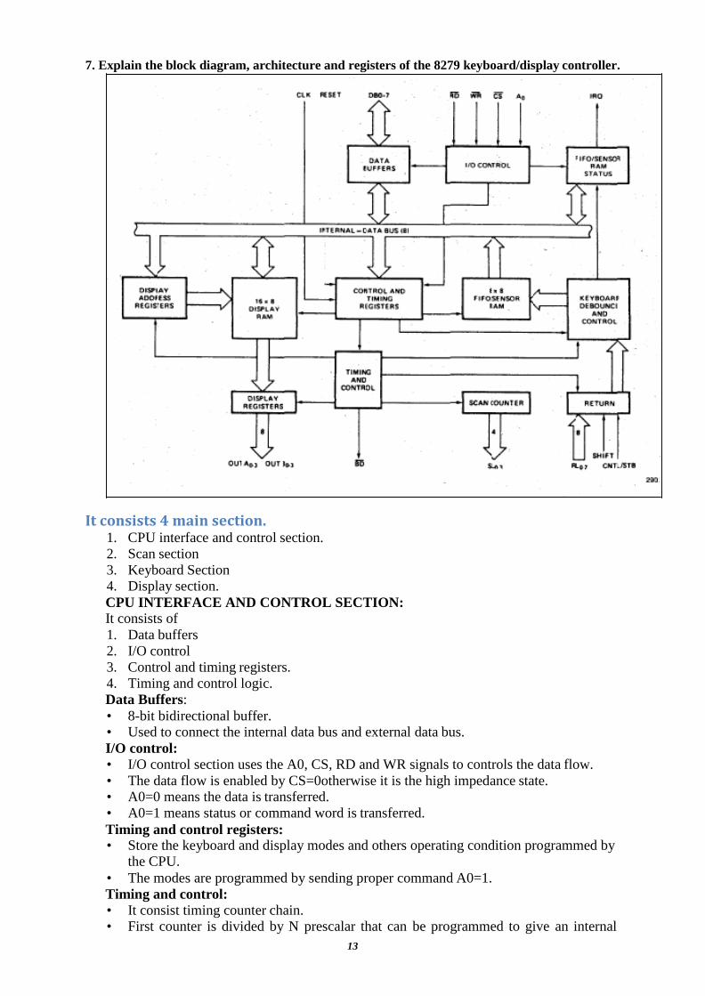
7. Explain the block diagram, architecture and registers of the 8279 keyboard/display controller.
It consists 4 main section. 1. CPU interface and control section.
2. Scan section
3. Keyboard Section 4. Display section.
CPU INTERFACE AND CONTROL SECTION:
It consists of
1. Data buffers
2. I/O control
3. Control and timing registers.
4. Timing and control logic.
Data Buffers:
• 8-bit bidirectional buffer. • Used to connect the internal data bus and external data bus.
I/O control:
• I/O control section uses the A0, CS, RD and WR signals to controls the data flow.
• The data flow is enabled by CS=0otherwise it is the high impedance state. • A0=0 means the data is transferred.
• A0=1 means status or command word is transferred.
Timing and control registers: • Store the keyboard and display modes and others operating condition programmed by
the CPU.
• The modes are programmed by sending proper command A0=1.
Timing and control:
• It consist timing counter chain. • First counter is divided by N prescalar that can be programmed to give an internal

14
frequency of 100 KHz.
SCAN SECTION
• It has two modes,
1. Encoded mode 2. Decoded mode.
ENCODED MODE:
• It provide binary count from 0000 to 1111 by four scan lines (SC3-SC0) by active high inputs.
• It is externally decoded to provide 16 scan lines
• Display use all 16 lines to interface 16 digit 7 segment display. • But keyboard use only 8 scan lines out of 16 lines.
DECODED MODE:
• In this mode, the internal decoder decodes the least 2 significant bits. • It is provide four possible combination from (SC0-SC3) such as 1110, 1101, 1011 and
0111.
• This four active low outputs line is used to directly to interface 4 –digit 7-segment
display ,8*4 matrix keyboard
KEYBOARD SECTION
This is consist of,
• Return buffers.
• Keyboard denounce control.
• FIFO / sensor RAM.
• FIFO / sensor RAM status.
Return buffers: • 8 return lines (RL7-RL0) are buffered and latched by when each row scan in scanned
keyboard or sensor matrix mode.
• In strobed mode, the contents of return lines are transferred to FIFO Ram.
Keyboard Debounce and Control:
• It is enabled only when keyboard mode is selected.
• In this mode, return lines are scanned whether any keys are closed in the row.
• If debounce circuit is detect any closed switch it wait about 10 msec.
• It is continued, the status of SHIFT and CONTROL keys are transferred into RAM.
• FIFO/SENSOR RAM:
• This is a dual function of 8*8 RAM.
• In scanned key board mode and Strobed input mode, it is FIFO. • Each new entry is written into successive RAM position and read in the order of
entry.
• In sensor matrix mode it is a sensor RAM.
• Each sensor RAM is loaded with corresponding sensor RAM status.
• FIFO/SENSOR RAM status:
• This is used to tell the status of FIFO/SENSOR RAM. • The status of logic also makes IRQ signal is High, When FIFO is empty.
DISPLAY SECTION:
It consists of,
1. Display RAM.
2. Display Address registers. 3. Display registers.
DISPLAY RAM:
• It is a 16*8 RAM.
• Which stores 16 digits display codes.
• It can be accessed by CPU directly.
• In Decoded mode, 8279 uses only first four location of Display RAM.
• In Encoded mode, 8279 uses only first eight location of Display RAM. • And all 16 location for 16 digits display.
15
DISPLAY ADDRESS REGISTERS:
• Used to hold address of the byte currently write or read by the CPU and scan count
value.
• In auto increment mode, address in the register is automatically incremented for each
write or read.
DISPLAY REGISTERS:
• It is a two 4-bit registers such as, A and B.
• They hold the bit patterns of character to be displayed. • The content of display registers A and B can B blanked and inhibited individually.
8. (i) Explain the advantages of using the keyboard and display controller chips in microprocessor based system.
When keyboard and display controller chips are used, it takes care of all tasks
involved in keyboard scanning and display refreshing. Hence, the processor is relieved
from the task of keyboard scanning, debouncing, keyboard generation and display
refreshing and so the processor time can be more efficiently used for computing.
(ii) Write a program using RST 5.5 interrupt to get an input from keyboard and display it.
MVI A, OEH SIM EI MVI A, 01000000 OUT 41H IN 40H ANI 00111111 STA IBUFF MVI A, 90H OUT 41H MVI A, CODE OUT 40H RIM RET
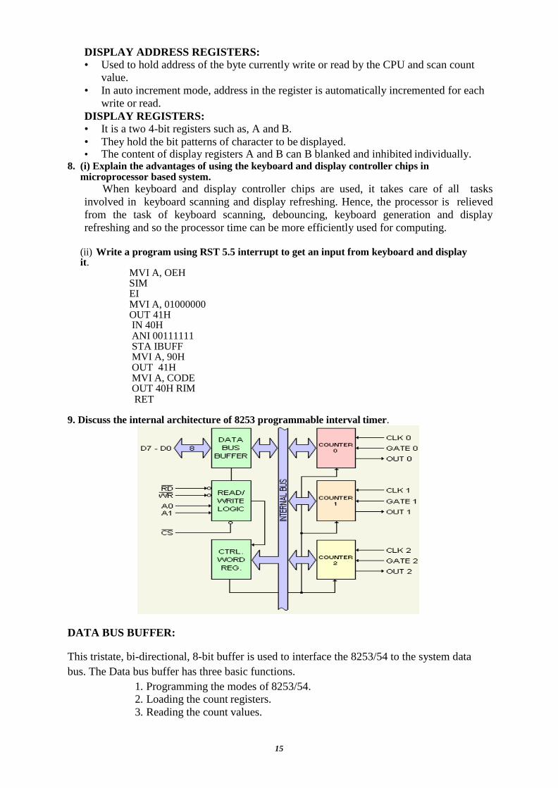
9. Discuss the internal architecture of 8253 programmable interval timer.
DATA BUS BUFFER:
This tristate, bi-directional, 8-bit buffer is used to interface the 8253/54 to the system data
bus. The Data bus buffer has three basic functions.
1. Programming the modes of 8253/54. 2. Loading the count registers.
3. Reading the count values.

16
READ/WRITE LOGIC:
The Read/Write logic has five signals: RD, WR, CS and the address lines A0 and A1. In the
peripheral I/O mode, the RD, and WR signals are connected to IOR and IOW, respectively.
In memory-mapped I/O, these are connected to MEMR and MEMW. Address lines A0 and
A1 of the CPU are usually connected to lines A0 and A1 of the 8253/54, and CS is tied to a
decoded address. The control word register and counters are selected according to the signals
on lines A0 and A1.
Control Word Register:
This register is accessed when lines A0 and A1 are at logic 1. It is used to write a command
word which specifies the counter to be used (binary or BCD), its mode, and either a read or
write operation.
Counters:
These three functional blocks are identical in operation. Each counter consists of a single, 16
bit, pre-settable, down counter. The counter can operate in either binary or BCD and its input,
gate and output are configured by the selection of modes stored in the control word register.
The counters are fully independent. The programmer can read the contents of any of the three
counters without disturbing the actual count in process
10. Draw the block diagram of 8237 DMA controller and explain each block.
• A DMA controller is a device, usually peripheral to a CPU that is programmed to perform
a sequence of data transfers on behalf of the CPU.
• A DMA controller can directly access memory and is used to transfer data from one
memory location to another, or from an I/O device to memory and vice versa.
• A DMA controller manages several DMA channels, each of which can be programmed to
perform a sequence of these DMA transfers. Devices, usually I/O peripherals, that acquire
data that must be read (or devices that must output data and be written to) signal the DMA
controller to perform a DMA transfer by asserting a hardware DMA request (DRQ)
signal. A DMA request signal for each channel l is routed to the DMA controller. This
signal is monitored and responded to in much the same way that a processor handles
interrupts.
• When the DMA controller sees a DMA request, it responds by performing one or many
data transfers from that I/O device into system memory or vice versa.

17
Functional Description
8237 ARCHITECTURE:
• The 82C37A direct memory access controller is designed to improve the data transfer rate in systems which must transfer data from an I/O device to memory, or move a block of memory to an I/O device.
• It will also perform memory to memory block moves, or fill a block of memory with data from a single location.
• Operating modes are provided to handle single byte transfers as well as discontinuous data streams, which allows the 82C37A to control data movement with software transparency.
• The DMA controller is a state driven address and control signal generator, which permits data to be transferred directly from an I/O device to memory or vice versa without ever being stored in a temporary register.
18
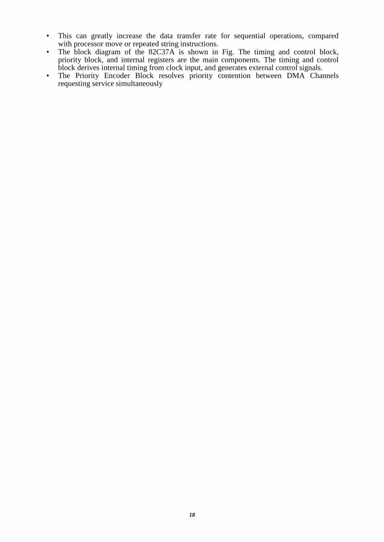
• This can greatly increase the data transfer rate for sequential operations, compared with processor move or repeated string instructions.
• The block diagram of the 82C37A is shown in Fig. The timing and control block, priority block, and internal registers are the main components. The timing and control block derives internal timing from clock input, and generates external control signals.
• The Priority Encoder Block resolves priority contention between DMA Channels requesting service simultaneously