ee40fa09 final exam solutions - university of california...
TRANSCRIPT

EECS 40, Fall 2009 Final Exam
Dec 15, 2009
Total Time Allotted: 3 hours
DO ALL WORK ON EXAM PAGES (Exam paper has a total of 9 pages including cover page)
1. Closed book exam. You are allowed to bring 3 sheets (8.5” x 11”) of notes. 2. You can use a calculator. NO cell phone or computer. 3. If you put down the wrong answer, partial credits will be given only if you show the
correct steps. 4. Points will be taken off for answers without units.
Last (Family) Name:______Solutions_______
First Name: ________________________________________________________
Student ID: _________________Discussion Session (# or TA): ___________________
Signature: _________________________________________________________
Problem 1 (18 points)
Problem 2 (25 Points)
Problem 3 (22 Points)
Problem 4 (25 Points)
Problem 5 (25 points)
Problem 6 (15 Points)
Problem 7 (15 points)
Problem 8 (25 Points)
Problem 9 (30 points)
TOTAL (200 points)

Problem 1 Diode Circuits (18 points total) All pn diodes shown below have a voltage drop of 0.6V when they are “ON”.
Indicate in the table whether the diodes D1A, D1B and D2 are ON/OFF with the given VA and VB values ( 1point each) . Also give the corresponding VOUT numerical values (3 points each) . NO PARTIAL CREDIT WILL BE GIVEN FOR THIS PROBLEM.
VA VB D1A (ON/OFF) D1B(ON/OFF) D2(ON/OFF) VOUT (sign and numerical value)
0V
0V ON ON ON 0V
0V
+4V ON OFF ON 0V
+4V
+4V OFF OFF ON +0.7V
VA=0V, VB=0V, D1Ais ON, D1B is ON, VX=+0,6V. D2 is ON. VOUT=0V VA=0V, VB=+4V, D1A is ON, D1B is OFF, VX=+0,6V. D2 is ON. VOUT=0V VA=+4V, VB=+4V, D1A is OFF, D1B is OFF, D2 is ON , Current through D2 = (4-(-2)-0.6)/10kΩ = 5.4x10⁻⁴A VOUT= -2V+5kΩ x5.4x10-4A= -2V+2.7V=+0.7V Note: VX= 4V-5kΩ x5.4x10-4A= 4-2.7V= +1.3V (consistent with D2 ON)

Problem2: MOSFET Amplifier (25 points total)
Consider the N-channel MOSFET amplifier given above. iDS =K2
(vGS −VT )2, VDD=5V, RL=2kΩ,
K=1mA/V2, VT=1V. You can ignore rd of the MOSFET. CC is the input coupling capacitor. You can assume it is infinitely large.
a) (3 points) Derive an expression for the transistor bias point VGSQ as a function of VDD,
Ra and Rb.
This is just a resistive divider,VGS =VDDRb
Rb + Ra
b) (10 points) Determine the required ratio Ra/Rb such that the MOSFET gm =1mA/V.
Remember that gm is defined as ∂IDS
∂VGS
.
First calculate VGS from the equation for gm
gm =∂IDS
∂VGS
= K(VGS −VT ) =1mA /V
=1mA /V 2(VGS −1V ) =1mA /V(VGS −1V ) =1VVGS = 2V
Next use the result from part a to determine the required rato

VGS =VDDRb
Rb + Ra
= 5V Rb
Rb + Ra
= 2V
Rb
Rb + Ra
=25
Ra =1.5Rb
c) (6 points) What is the voltage bias point of the output VoutQ? (If you cannot calculate a
numerical answer leave the answer it in terms of the given circuit parameter values, Ra and Rb.). Use the results from part(b).
First solve for the quiescent current, then calculate the voltage:
IDS =K2
(VGS −VT )2 =1mA /V 2
2(2V −1V )2 = 0.5mA
VOUT =VDD − IDSRL = 5V − 0.5mA ⋅ 2kΩ= 4V
In terms of circuit parameters:
IDS =
K2
(VGS −VT )2 =K2
(VDDRb
Rb + Ra
−VT )2
VOUT =VDD − IDSRL =VDD −K2
(VDDRb
Rb + Ra
−VT )2 RL
d) (6 points) Draw the small-signal model for the amplifier and calculate the gain vout/vin.
Clearly label the component values and small-signal voltages vin and vout.Us ethe results from part(b).
The small-signal model:
The gain is just gm*RL=2

Problem 3 MOSFET and diode: Qualitative behavior (22 points total) a) You are given the following circuit, and the magical ability to change each of the following input parameters independently: V1, V2, K, VT. You also measure each of the following parameters: I1, I2, gm, rd. Indicate in the table how an increase in each of the “input” parameters changes each of the “output” parameters. Please use these symbols: ↑ = increase, ↓ = decrease, ‐‐ = no change. You may assume that the transistor is in saturation.
I1 I2 gm rd
V1 -- ↑ ↑ ↓
V2 -- ↑ ↑ ↓
K -- ↑ ↑ ↓
VT -- ↓ ↓ ↑
I1 is always zero, and is not affected by any of the input parameters.
• I2 increases with K, V1 and V2, and decreases with VT.
• gm varies the same way as I2.
• rd varies in the opposite way from I2.

Problem 3 continued (b) The following diode circuit and the parameters are shown in the table. Fill in the table
how an increase in each of the “input” parameters VD,IS,VTh changes each of the “output” parameters. Please use these symbols:
↑ = increase, ↓ = decrease, ‐‐ = no change. VTh is the thermal voltage (kT/q) and rd is the small signal resistance
The diode I‐V characteristics is : ThDThD V/V
SV/V
SD eI)1e(II ≅−=
ID rd
VD ↑ ↓
IS ↑ ↓
VTh ↓ ↑
For the diode, we have the following equations:
(If you didn’t have the equation for rd on your formula sheet, you can easily derive it, or estimate from a sketch of ID.) We see that:
• ID increases with IS and VD, and decreases with VTh.
• rd varies in the opposite way as ID. For the dependence on VTh, both the numerator and the denominator cause rd to increase.

Problem 4 Diodes and transients (25 points total) A circuit with input resistance Ri uses a Zener diode with breakdown voltage VBR (=5V) to protect itself from large input voltages. For this problem, we will augment the diode model used in class to include the diode’s capacitance due to the p-n junction. The equivalent circuit of the Zener diode in the reverse-bias region is modeled as a capacitor CD if there is no breakdown. The diode is modeled as a short plus VBR if there is breakdown (see figures at right) A large input voltage step with magnitude Vs is connected to the circuit through a resistance Rs. It is given that Vs = 14V and V1 (t=0) =0 . Let Ri=Rs.
(a) Find an analytical expression for the time constant τ in terms of RS, Ri and CD when the diode is not conducting. (10 pts)
The natural response in the reverse-bias region can be found by setting the forcing function to zero and substituting a capacitor for the diode:
The resistors now appear in parallel. We can find the time constant in terms of the equivalent (parallel) resistance:

(b) Sketch the voltage V1, versus time in units of τ, on the axes given. Find the voltage at t = τ, 2τ, 3τ and show the values on your plot. (15 pts) [ Hint: Apply the method of assumed states for each time t and check consistency]
a)
Observe that this is a first-order transient with initial value 0V. Ignoring the breakdown of the diode (i.e. assuming that the model valid at t = 0 remains valid for all time), the final value is given by a voltage divider consisting of two equal resistors: This allows us to find the value at t = τ: We can use the same approach to find the value at t = 2τ: But this is greater than the diode’s breakdown voltage. Therefore, somewhere between τ and 2τ, the diode will start to conduct, and clip off any further increase in voltage. Therefore,
0
v1 (V)
t/τ 1 2 3
8
6
4
2 4.4 V
5 V 5 V
0
V1 (V)
t/τ 1 2 3
8
6
4
2
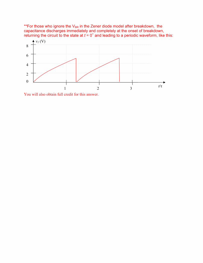
**For those who ignore the VBR in the Zener diode model after breakdown, the capacitance discharges immediately and completely at the onset of breakdown, returning the circuit to the state at t = 0+ and leading to a periodic waveform, like this:
You will also obtain full credit for this answer.
0
v1 (V)
t/τ 1 2 3
8
6
4
2

Problem 5 Reactive Elements and Power (25 points total) You are driving a sinusoidal signal v1 through a resistance RS, into a device with a large parasitic input capacitance C1 (=100pF) .Besides the capacitor, no other current flows into the device.
a) Does the current ii lead or lag the applied voltage vi? (5 pts) The current leads the voltage, because a capacitor is present, which differentiates voltage. Suppose the applied voltage is a sine function. At t = 0, the voltage is zero, but because the voltage is increasing, current is already flowing in the capacitor.
b) Suppose Vc (t) is known to be 4•cos(ωt) V. Calculate the current i1(t) at 22 MHz. (5 pts) First, find the current ii :
c) Calculate the peak power dissipated in the capacitor at 22 MHz? (10 pts) Now we can find the power after knowing current, using the derivation described on Hambley p. 226:

The peak power is just the amplitude of this waveform:
Note: The time-average power in a reactive element always averages to zero (as we can see in this particular case from the fact that it is a sinusoid).
d) You want to reduce the peak power consumption by adding an extra parallel element Zp as shown. Indicate whether you will choose a resistor, inductor, or capacitor, and justify your choice in 10 words or less (further words will not be graded). (5 pts)
In order to reduce the power, we must reduce the current i1. Only an inductor can achieve this. Possible justifications include:
• “Resonance” give infinite impedance of LC.
• “Increase impedance after resistor”
• “Positive reactance cancels negative reactance”
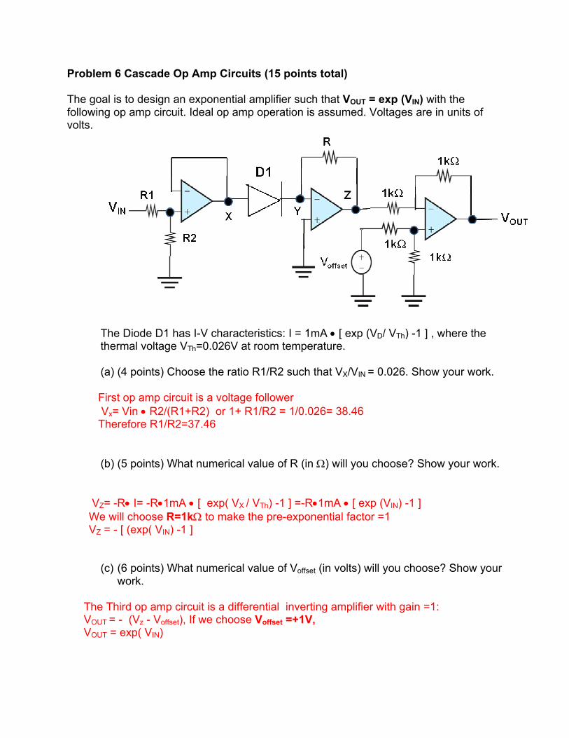
Problem 6 Cascade Op Amp Circuits (15 points total) The goal is to design an exponential amplifier such that VOUT = exp (VIN) with the following op amp circuit. Ideal op amp operation is assumed. Voltages are in units of volts.
The Diode D1 has I-V characteristics: I = 1mA • [ exp (VD/ VTh) -1 ] , where the thermal voltage VTh=0.026V at room temperature. (a) (4 points) Choose the ratio R1/R2 such that VX/VIN = 0.026. Show your work.
First op amp circuit is a voltage follower Vx= Vin • R2/(R1+R2) or 1+ R1/R2 = 1/0.026= 38.46 Therefore R1/R2=37.46
(b) (5 points) What numerical value of R (in Ω) will you choose? Show your work. VZ= -R• I= -R•1mA • [ exp( VX / VTh) -1 ] =-R•1mA • [ exp (VIN) -1 ] We will choose R=1kΩ to make the pre-exponential factor =1 VZ = - [ (exp( VIN) -1 ]
(c) (6 points) What numerical value of Voffset (in volts) will you choose? Show your work.
The Third op amp circuit is a differential inverting amplifier with gain =1: VOUT = - (Vz - Voffset), If we choose Voffset =+1V, VOUT = exp( VIN)

Problem 7 Wave Shaping Circuits (15 points total) (A) (10 points) The following diode-capacitor circuit has vin(t)= Vm•sin(ωt) shown in
the graph. The diode has perfect rectifier behavior. vC is initially equal to 0 at t=0. Sketch vC(t) using a dash line and sketch vout(t) as a dotted line in the same graph for all times t.
(B) (5 points) A DC voltage source VB=+1V is added to the diode-capacitor circuit. Sketch only the steady-state vout(t) in the same graph (i.e. after one cycle of Vin)

Problem 7 answers (A) Vout(t) = Vin(t) - Vc(t)
(B) You only have to show the steady state waveform to obtain full credit.

Problem 8 Miscellaneous Questions (25 points total)
Please circle either True (T) or False(F) for the following statements: T F Miniaturization gives faster integrated circuit performance T F A state-of-the-art solid-state transistor has critical dimensions on the order of 45 nm. T F The maximum power that a solar cell can deliver in practice equals isc • voc. T F KVL and KCL can be applied to circuits with nonlinear circuit elements T F Superposition Principle can be applied to circuits with nonlinear circuit elements T F CMOS logic circuits dissipated power only during switching T F Ideal capacitors and inductors have zero instantaneously power at all times. T F An ideal OP Amp has zero gain for common-mode input signal T F A real OP Amp voltage follower circuit has very large input resistance T F For MOSFETs with fixed VGS, triode region has less current than saturation region. T F All combinatorial logic functions can be synthesized by NOR gates alone. T F Mesh analysis has fewer independent equations than Nodal Analysis in general T F The Transresistance Amplifier Model uses a current-controlled voltage source. T F Amplifier will have no waveform distortion if phase shift is linear proportional to frequency T F We can use SOP Method to simplify sequential logic design. T F Bias and offset current sources are desirable for Differential Amplifiers. T F Harmonic distortion of an amplifier will become bigger with larger signal amplitudes. T F Overshooting of amplifier with impulse input is related to the amplifier’s bandwidth T F A pure resistive load has maximum reactive power. T F A full wave rectifier circuit requires at least 4 diodes T F Magnitude Bode Plot of any RLC circuit cannot have a slope larger than 20 dB/decade T F A Ripple Counters requires both the input signal and a separate clock signal. T F MOSFET with the drain tied to the gate will operate in the saturation mode when it is ON. T F A pn diode can be used as a photodetector. T F “Don’t care” as output in truth tables will give simpler Boolean algebraic expressions.

Problem 9 LAB Questions (30 points total) (A ) Write the names of circuit components shown below. a.)__Potentiometer_________ (1pt) b.)_____Inductor____________ (1pt) c.) _______Diode______________(1pt) d.) _________Transistor_______(1pt) e.) ___________Inductor______(1pt) f.) ___________Capacitor_____(1pt) (B)- Write the name of the instruments’ labeled below.
a.)_____ Oscilloscope _____ (1pt) b.)____Function Generator__ (1pt) c.) _The Digital Multimeter___(1pt) d.) ___Power supply_____(1pt) e.) ______Breadboard______(1pt) f.) _Soldering Iron/Solder____(1pt)

(C ) Which instrument do we use to measure current and voltage? (2pt)
• Multimeter • Avometer
(D) Draw the missing components of the boost converter circuit. (6pt)
(E) Write the two basic components of a microcontroller. (2pt)
• CPU • RAM • In/Out Ports • Timer
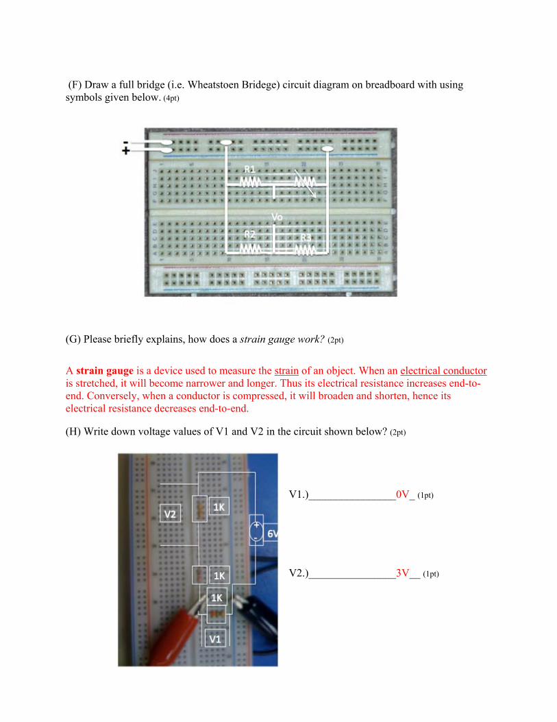
(F) Draw a full bridge (i.e. Wheatstoen Bridege) circuit diagram on breadboard with using symbols given below. (4pt)
(G) Please briefly explains, how does a strain gauge work? (2pt) A strain gauge is a device used to measure the strain of an object. When an electrical conductor is stretched, it will become narrower and longer. Thus its electrical resistance increases end-to-end. Conversely, when a conductor is compressed, it will broaden and shorten, hence its electrical resistance decreases end-to-end. (H) Write down voltage values of V1 and V2 in the circuit shown below? (2pt)
V1.)________________0V_ (1pt)
V2.)________________3V__ (1pt)