ee3209 - communications laboratory lab manual
TRANSCRIPT

EE3209 - Communication Laboratory © 2017 of the California State University, Los Angeles | College of Engineering, Computer Science, and Technology | Department of Electrical and Computer Engineering
1
EE3209 - Communications Laboratory
Lab Manual
California State University, Los Angeles
College of Engineering, Computer Science, and Technology
Department of Electrical and Computer Engineering
Instructor: Khashayar Olia

EE3209 - Communication Laboratory © 2017 of the California State University, Los Angeles | College of Engineering, Computer Science, and Technology | Department of Electrical and Computer Engineering
2
Lab 5: Double Sideband-Suppressed Carrier V2.0
Objective:
This laboratory exercise introduces Double-Sideband Suppressed-Carrier modulation. A simple scheme for
phase and frequency synchronization is introduced in implementing the demodulator.
Background:
Double-Sideband Suppressed-Carrier
Amplitude Modulation (AM), as the oldest method of modulation, is simple and relatively inexpensive to
build. These advantages make it popular for simple applications, but it is inherently inefficient at least in
two main categories:
1. AM is wasteful of transmitted power because the largest part of the transmitted power is contained
in the carrier. We know that AM transmitted signal is defined by Eq. 1:
𝑠(𝑡) = 𝐴𝑐 [1 + 𝜇𝑚(𝑡)
𝑚𝑝(𝑡)] 𝑐𝑜𝑠 (2𝜋𝑓𝑐𝑡 + 𝜑)
= 𝐴𝑐 𝑐𝑜𝑠(2𝜋𝑓𝑐𝑡 + 𝜑) + 𝜇𝑚(𝑡)
𝑚𝑝(𝑡)𝑐𝑜𝑠 (2𝜋𝑓𝑐𝑡 + 𝜑)
Eq. 1
where the first term only contains the carrier wave, therefore represents a waste of power.
2. AM is wasteful of bandwidth because the upper and lower sidebands of an AM signal are related
to each other which means by knowing the amplitude and phase of one sideband, we can determine
and construct the other sideband.
In order to overcome the limitations of AM, some changes must be applied to the current AM architecture.
Double Sideband-Suppressed Carrier (DSB-SC) and Single Sideband (SSB) modulations are the
modified forms of simple AM architecture which overcome the AM limitations and result in more complex
systems.

EE3209 - Communication Laboratory © 2017 of the California State University, Los Angeles | College of Engineering, Computer Science, and Technology | Department of Electrical and Computer Engineering
3
In DSB-SC scheme, the carrier is simply not transmitted and the modulated wave only consists of upper
and lower sideband. In this regard, the DSB-SC doesn’t waste the transmitted power while the channel
bandwidth is the same. In SSB scheme, the modulated wave consists only of either the upper sideband or
lower sideband therefore it uses less bandwidth. In this lab, we study and experiment the DSB-SC
transmitter and receiver.
DSB-SC modulation is identical to AM, except that the carrier is omitted. Basically, DSB-SC is defined as
the product of the message signal 𝑚(𝑡) and the carrier wave 𝐴𝑐𝑐𝑜𝑠 (2𝜋𝑓𝑐𝑡), so we can write the DSB-SC
signal:
𝑠(𝑡) = 𝐴𝑐𝑚(𝑡) 𝑐𝑜𝑠(2𝜋𝑓𝑐𝑡)
Eq. 2
where 𝑓𝑐 is carrier frequency. The device used to generate the DSB-SC modulated wave is usually referred
to as a product modulator [1]. Figure 1 illustrates the waveform of 𝑚(𝑡), 𝑐(𝑡) and 𝑠(𝑡):
Figure 1: DSB-SC Modulated signal
EE3209 - Communication Laboratory © 2017 of the California State University, Los Angeles | College of Engineering, Computer Science, and Technology | Department of Electrical and Computer Engineering
4
Note the phase reversal of the carrier wave when the message signal 𝑚(𝑡) crosses zero. This means that the
envelop of a DSB-SC modulated signal is different from the message signal so the simple envelope detector
used for amplitude demodulation is not useful anymore.
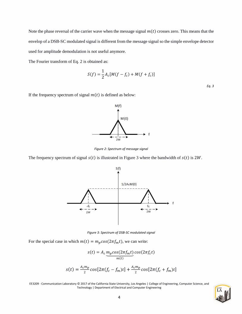
The Fourier transform of Eq. 2 is obtained as:
𝑆(𝑓) =1
2𝐴𝑐[𝑀(𝑓 − 𝑓𝑐) + 𝑀(𝑓 + 𝑓𝑐)]
Eq. 3
If the frequency spectrum of signal 𝑚(𝑡) is defined as below:
Figure 2: Spectrum of message signal
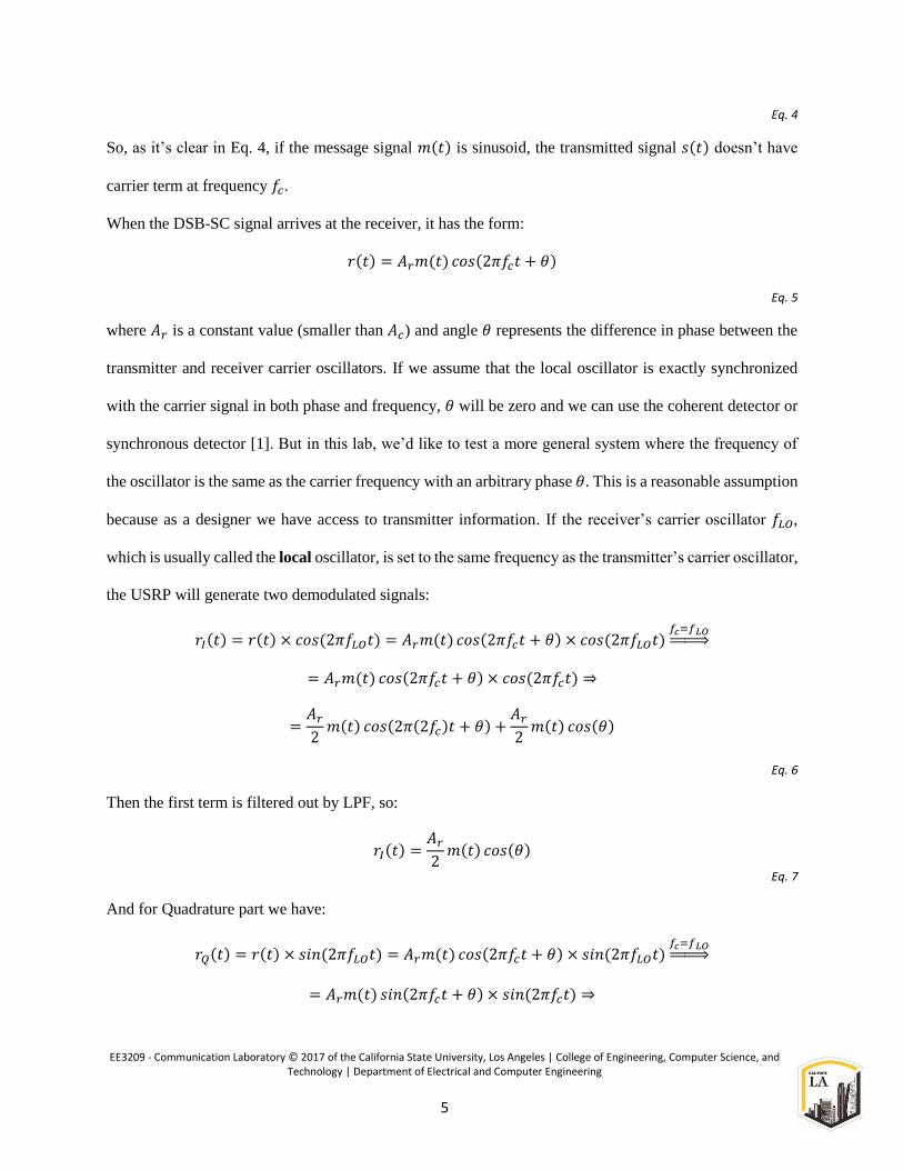
The frequency spectrum of signal 𝑠(𝑡) is illustrated in Figure 3 where the bandwidth of 𝑠(𝑡) is 2𝑊.
Figure 3: Spectrum of DSB-SC modulated signal
For the special case in which 𝑚(𝑡) = 𝑚𝑝𝑐𝑜𝑠 (2𝜋𝑓𝑚𝑡), we can write:
𝑠(𝑡) = 𝐴𝑐𝑚𝑝𝑐𝑜𝑠 (2𝜋𝑓𝑚𝑡)⏟ 𝑚(𝑡)
𝑐𝑜𝑠(2𝜋𝑓𝑐𝑡)
𝑠(𝑡) =𝐴𝑐𝑚𝑝
2𝑐𝑜𝑠[2𝜋(𝑓𝑐 − 𝑓𝑚)𝑡] +
𝐴𝑐𝑚𝑝
2𝑐𝑜𝑠[2𝜋(𝑓𝑐 + 𝑓𝑚)𝑡]
EE3209 - Communication Laboratory © 2017 of the California State University, Los Angeles | College of Engineering, Computer Science, and Technology | Department of Electrical and Computer Engineering
5
Eq. 4
So, as it’s clear in Eq. 4, if the message signal 𝑚(𝑡) is sinusoid, the transmitted signal 𝑠(𝑡) doesn’t have
carrier term at frequency 𝑓𝑐.
When the DSB-SC signal arrives at the receiver, it has the form:
𝑟(𝑡) = 𝐴𝑟𝑚(𝑡) 𝑐𝑜𝑠(2𝜋𝑓𝑐𝑡 + 𝜃)
Eq. 5
where 𝐴𝑟 is a constant value (smaller than 𝐴𝑐) and angle 𝜃 represents the difference in phase between the
transmitter and receiver carrier oscillators. If we assume that the local oscillator is exactly synchronized
with the carrier signal in both phase and frequency, 𝜃 will be zero and we can use the coherent detector or
synchronous detector [1]. But in this lab, we’d like to test a more general system where the frequency of
the oscillator is the same as the carrier frequency with an arbitrary phase 𝜃. This is a reasonable assumption
because as a designer we have access to transmitter information. If the receiver’s carrier oscillator 𝑓𝐿𝑂,
which is usually called the local oscillator, is set to the same frequency as the transmitter’s carrier oscillator,
the USRP will generate two demodulated signals:
𝑟𝐼(𝑡) = 𝑟(𝑡) × 𝑐𝑜𝑠 (2𝜋𝑓𝐿𝑂𝑡) = 𝐴𝑟𝑚(𝑡) 𝑐𝑜𝑠(2𝜋𝑓𝑐𝑡 + 𝜃) × 𝑐𝑜𝑠 (2𝜋𝑓𝐿𝑂𝑡)𝑓𝑐=𝑓𝐿𝑂⇒
= 𝐴𝑟𝑚(𝑡) 𝑐𝑜𝑠(2𝜋𝑓𝑐𝑡 + 𝜃) × 𝑐𝑜𝑠 (2𝜋𝑓𝑐𝑡) ⇒
=𝐴𝑟2𝑚(𝑡) 𝑐𝑜𝑠(2𝜋(2𝑓𝑐)𝑡 + 𝜃) +
𝐴𝑟2𝑚(𝑡) 𝑐𝑜𝑠(𝜃)
Eq. 6
Then the first term is filtered out by LPF, so:
𝑟𝐼(𝑡) =𝐴𝑟2𝑚(𝑡) 𝑐𝑜𝑠(𝜃)
Eq. 7
And for Quadrature part we have:
𝑟𝑄(𝑡) = 𝑟(𝑡) × 𝑠𝑖𝑛 (2𝜋𝑓𝐿𝑂𝑡) = 𝐴𝑟𝑚(𝑡) 𝑐𝑜𝑠(2𝜋𝑓𝑐𝑡 + 𝜃) × 𝑠𝑖𝑛 (2𝜋𝑓𝐿𝑂𝑡)𝑓𝑐=𝑓𝐿𝑂⇒
= 𝐴𝑟𝑚(𝑡) 𝑠𝑖𝑛(2𝜋𝑓𝑐𝑡 + 𝜃) × 𝑠𝑖𝑛(2𝜋𝑓𝑐𝑡) ⇒

EE3209 - Communication Laboratory © 2017 of the California State University, Los Angeles | College of Engineering, Computer Science, and Technology | Department of Electrical and Computer Engineering
6
=𝐴𝑟2𝑚(𝑡) 𝑠𝑖𝑛(2𝜋(2𝑓𝑐)𝑡 + 𝜃) +
𝐴𝑟2𝑚(𝑡) 𝑠𝑖𝑛(𝜃)
Eq. 8
After filtering the first term we have:
𝑟𝑄(𝑡) =𝐴𝑟2𝑚(𝑡) sin(𝜃)
Eq. 9
The Fetch Rx Data VI provides these demodulated signals as a single complex-valued signal:
�̃�(𝑡) = 𝑟𝐼(𝑡)+ 𝑗𝑟𝑄(𝑡)⟹
=𝐴𝑟2𝑚(𝑡) 𝑐𝑜𝑠(𝜃) + 𝑗
𝐴𝑟2𝑚(𝑡) 𝑠𝑖𝑛(𝜃) ⟹
�̃�(𝑡) =√2𝐴𝑟2𝑚(𝑡)𝑒𝑗𝜃
Eq. 10
It is tempting to suppose that the message 𝑚(𝑡) can be extracted from �̃�(𝑡) by taking the magnitude of the
complex signal. Unfortunately, the magnitude of �̃�(𝑡) is different from the message signal 𝑚(𝑡) where the
absolute value represents unwanted distortion of the message signal:
|�̃�(𝑡)| = |√2𝐴𝑟2𝑚(𝑡)𝑒𝑗𝜃| =
√2𝐴𝑟2|𝑚(𝑡)|
Eq. 11
So as we expect earlier, the simple envelope detector does not work for DSB-SC modulation.
It is more productive to use the in-phase (real part) signal 𝑟𝐼(𝑡) given in Eq. 7. The 𝑐𝑜𝑠(𝜃) factor of 𝑟𝐼(𝑡)
represents a gain constant. Unfortunately, the value of this gain constant is not under user control, and might
be small if 𝜃 turns out to have a value near ± 𝜋 2⁄ . Moreover, if the receiver’s oscillator and transmitter’s
oscillator differ slightly in frequency, then the phase error 𝜃 will change with time, causing 𝑟𝐼(𝑡) to fade in
and out. The next section discusses how we will compensate for the 𝑐𝑜𝑠(𝜃) term.
Phase Synchronization
There are a number of techniques that can be used to eliminate the 𝑐𝑜𝑠(𝜃) phase-error term such as Costas

EE3209 - Communication Laboratory © 2017 of the California State University, Los Angeles | College of Engineering, Computer Science, and Technology | Department of Electrical and Computer Engineering
7
receiver [1] which consists of two coherent detectors with a voltage-controlled oscillator that forms a
negative feedback to maintain the local oscillator in synchronism with the carrier signal. The method we
present here is different from Costas receiver but it is simple and easy to implement in LabVIEW. The basic
steps are:
1. Estimate 𝜃
2. Multiply �̃�(𝑡) by 𝑒−𝑗𝜃 to eliminate the phase:
�̃�(𝑡) × 𝑒−𝑗𝜃 =√2𝐴𝑟2𝑚(𝑡)𝑒𝑗𝜃 × 𝑒−𝑗𝜃
=√2𝐴𝑟2𝑚(𝑡)𝑒𝑗0
Eq. 12
3. Take the real part of Eq. 12:
𝑅𝑒 {√2𝐴𝑟2𝑚(𝑡)𝑒𝑗0} =
𝐴𝑟2𝑚(𝑡)
Eq. 13
Estimating 𝜃 requires several steps. Note first that the phase angle of �̃�(𝑡) will jump by ±𝜋 whenever 𝑚(𝑡)
changes sign. To eliminate these phase jumps, start by squaring �̃�(𝑡):
�̃�2(𝑡) =𝐴𝑟2
2𝑚2(𝑡)𝑒𝑗2𝜃
Eq. 14
Since the squared message 𝑚2(𝑡) never changes sign, the phase jumps are eliminated. The angle 2𝜃 can be
extracted using a Complex to Polar VI (Functions > Mathematics > Numeric > Complex palette). It turns
out to be helpful at this point to smooth variations in 2𝜃 caused by noise. The Median Filter (Functions >
Signal Processing > Filters palette) does a good job. The default values can be accepted for the left rank
and right rank parameters. Next the Unwrap Phase VI will remove jumps of ±2𝜋 (Functions > Signal
Processing > Signal Operations palette). Finally, dividing by two gives the desired estimate of the phase
error 𝜃. The block diagram in Figure 4 shows the entire phase synchronization process.

EE3209 - Communication Laboratory © 2017 of the California State University, Los Angeles | College of Engineering, Computer Science, and Technology | Department of Electrical and Computer Engineering
8
Figure 4: Phase Synchronization

EE3209 - Communication Laboratory © 2017 of the California State University, Los Angeles | College of Engineering, Computer Science, and Technology | Department of Electrical and Computer Engineering
9
Prelab
Transmitter
A template for the transmitter has been provided in the file “Lab5TxTemplate.vit”. This template contains
the four interface VI’s along with a message generator that is set to produce a message signal consisting
of three tones. Your task is to add blocks as needed to produce a DSB-SC signal, and then to pass the DSB-
SC signal into the while loop to the Write Tx Data block.
Transmitter Notes:
1. Use Eq. 2 in order to generate DSB-SC signal. Note 𝑐𝑜𝑠(2𝜋𝑓𝑐𝑡) is generated inside the USRP:
I. The message generator creates a signal that is the sum of a set of sinusoids of equal amplitude.
You can choose the number of sinusoids to include in the set, you can choose their frequencies,
and their common amplitude. In this template, the message generator has been provided with a
seed. This causes the initial phase angles of the sinusoids to be the same every time you run
the VI. As a result, the same message will be generated every time, which is useful to aid
debugging. To restore random behavior, set the seed to −1.
II. The DSB-SC signal you generate will be the In-Phase part 𝑆𝐼(𝑡). Remember that there is a
practical constraint imposed by the D/A converters in the USRP, so you need to scale down the
signals you generate so that the peak value of |�̃�(𝑛𝑇)| does not exceed 1. Use second output
of Quick Scale VI to scale down the message signal 𝑚(𝑡):
Figure 5: Quick Scale VI
III. For the Quadrature part 𝑆𝑄(𝑡), set up an array the same length as 𝑆𝐼(𝑡) containing all zeros. In
order to generate the same length array, as we learned in Lab 3 use Array Size icon (Functions
> Programming > Array > Array Size):
EE3209 - Communication Laboratory © 2017 of the California State University, Los Angeles | College of Engineering, Computer Science, and Technology | Department of Electrical and Computer Engineering
10
Figure 6: Array Size Icon
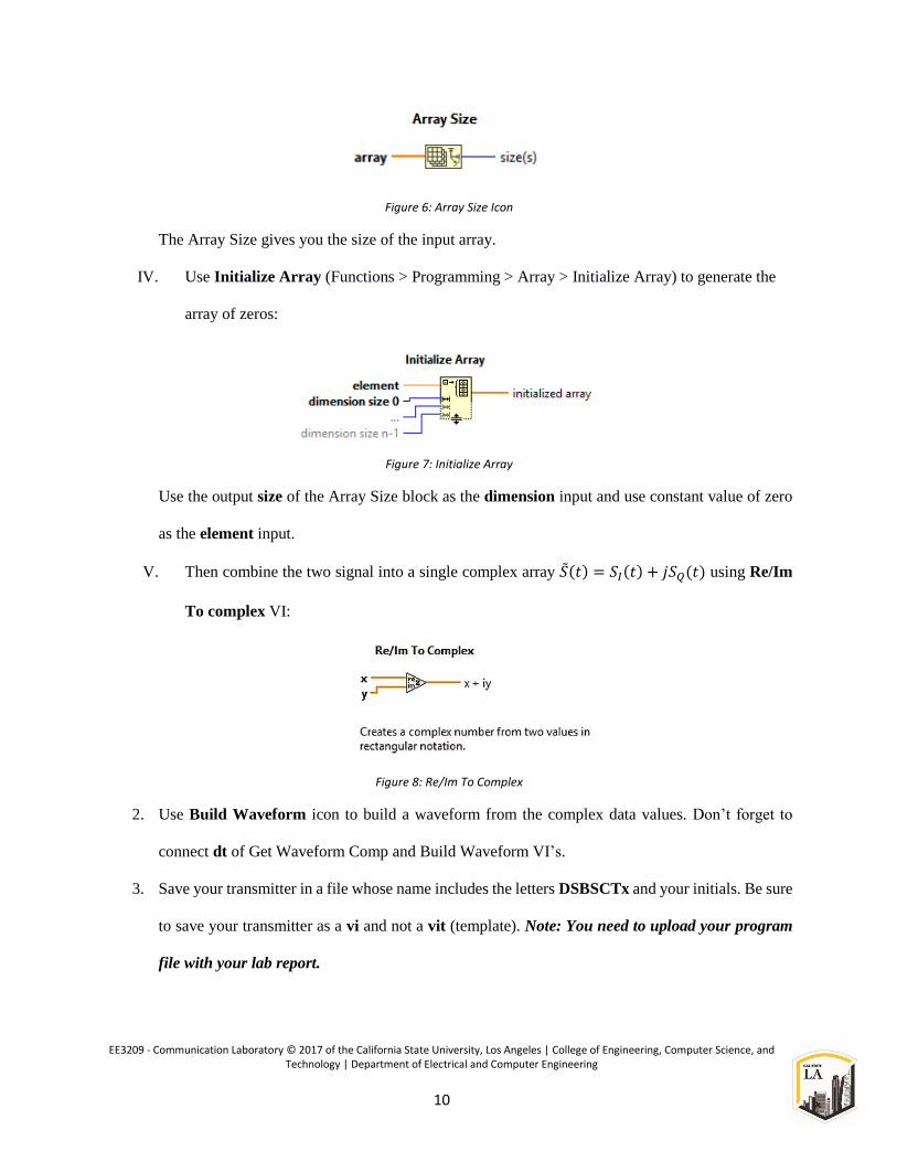
The Array Size gives you the size of the input array.
IV. Use Initialize Array (Functions > Programming > Array > Initialize Array) to generate the
array of zeros:
Figure 7: Initialize Array
Use the output size of the Array Size block as the dimension input and use constant value of zero
as the element input.
V. Then combine the two signal into a single complex array �̃�(𝑡) = 𝑆𝐼(𝑡) + 𝑗𝑆𝑄(𝑡) using Re/Im
To complex VI:
Figure 8: Re/Im To Complex
2. Use Build Waveform icon to build a waveform from the complex data values. Don’t forget to
connect dt of Get Waveform Comp and Build Waveform VI’s.
3. Save your transmitter in a file whose name includes the letters DSBSCTx and your initials. Be sure
to save your transmitter as a vi and not a vit (template). Note: You need to upload your program
file with your lab report.

EE3209 - Communication Laboratory © 2017 of the California State University, Los Angeles | College of Engineering, Computer Science, and Technology | Department of Electrical and Computer Engineering
11
Receiver
A template for the receiver has been provided in the file “Lab5RxTemplate.vit”. This template contains
the six interface VI’s along with a waveform graph on which to display your demodulated output signal.
The task is to complete the VI to demodulate the complex array returned by the Fetch Rx Data VI and
display the result. Include the phase synchronization (Figure 4) in your receiver. Also, to help in debugging,
include a graph to display the phase error 𝜃 vs. time.
Receiver Notes:
1. Build the phase synchronization of Figure 4 to demodulate the signal:
I. Use the provided Waveform Graph to show the phase error 𝜃 vs. time to help in debugging.
II. Use integer 5 for Left Rank of Median Filter.
Figure 9: Median Filter
III. Note that you need to display only the real part of the modulated signal, so use Complex to
Re/Im VI.
2. Use Build Waveform icon to build a waveform from the complex data values. Don’t forget to
connect dt of Get Waveform Comp and Build Waveform VI’s.
3. In order to compare the 𝑟𝐼(𝑡) without phase synchronization, connect the unmodulated signal to
another Complex to Re/Im.
4. Use another Build Waveform icon to build a waveform for unsynchronized output.
5. Now we want to show the synchronized and unsynchronized waveforms as a combined message
on a single graph:
I. As we learned in Lab 3, to build an array from the two generated messages, use the Build Array
(Functions > Programming > Array > Build Array) icon:

EE3209 - Communication Laboratory © 2017 of the California State University, Los Angeles | College of Engineering, Computer Science, and Technology | Department of Electrical and Computer Engineering
12
Figure 10: Build Array Icon
II. Use the provided Waveform Graph to show the combined messages.
6. Save your receiver in a file whose name includes the letters DSBSCRx and your initials. Be sure
to save your receiver as a vi and not a vit (template). Note: You need to upload your program file
with your lab report.
Lab Procedure:
1. Connect the loopback cable and attenuator between the TX 1 and RX 2 antenna connectors.
Connect the USRP to your computer with an Ethernet cable and plug in the power to the radio. At
this point LED’s D (firmware loaded) and F (power on) should be illuminated, as should the green
light on the left side of the Ethernet connector. Run LabVIEW and open the transmitter and receiver
VIs that you created in the prelab.
2. Ensure the transmitter and receiver VI’s are set up based on Table 1, Table 2 and Table 3.
3. Run the receiver VI (LED C will illuminate on the USRP if the radio is receiving data) then run
the transmitter VI (LED A will illuminate if the radio is transmitting data). After a few seconds,
stop the receiver using the STOP button, then stop the transmitter.
4. Use the horizontal zoom feature on the graph palette to expand the message waveform in the
transmitter VI and the demodulated output waveform in the receiver VI. (1 point)
Both waveforms should be identical, except for scaling. However, the demodulated output may be
inverted. This is a consequence of squaring the signal in the phase synchronization process. An
error of ±2𝜋 in the angle ±2𝜃 is no error at all, but when the angle is divided by two, the error
becomes ±𝜋. Save the graph in your lab report.

EE3209 - Communication Laboratory © 2017 of the California State University, Los Angeles | College of Engineering, Computer Science, and Technology | Department of Electrical and Computer Engineering
13
Table 1: Transmitter Settings
Field Settings
Device Name 192.168.10.2
IQ Rate 200 kS/sec
Carrier Frequency 915 MHz
Gain 0 dB
Active Antenna TX1
Table 2: Transmitter Message Settings
Field Message Settings
Start Frequency 10 Hz
Delta Frequency 100 Hz
Number of Tones 1
Modulation Index 1
Message Length 200,000 samples
Table 3: Receiver Settings
Field Settings
Device Name 192.168.10.2
IQ Rate 1 MS/sec
Carrier Frequency 915 MHz
Gain 0 dB
Active Antenna RX2
Number of Samples 200,000
Experiments:
Do the following experiments, plot the graphs in your report and describe the results:

EE3209 - Communication Laboratory © 2017 of the California State University, Los Angeles | College of Engineering, Computer Science, and Technology | Department of Electrical and Computer Engineering
14
1. Try using your AM receiver from Lab 2 (AMRXOffset.vi) to demodulate the DSB-SC signal. Note
that you will need to offset the transmitter frequency to 915.1 MHz. Run the transmitter and
receiver. Take a screenshot of both the transmitted message and the demodulated output. Be sure
to expand the time base so that the waveforms can be clearly seen. Was the envelope detector in
the AM receiver able to correctly demodulate the DSB-SC signal? Describe it in your lab report.
(2 points)
2. The phase synchronizer can also correct for modest frequency offsets. Use the DSB-SC transmitter
and receiver, and offset the frequency of the transmitter by 10 Hz. Run the transmitter and receiver.
Take a screenshot of the transmitted message, the unsynchronized demodulated output, and the
synchronized demodulated output. Be sure to expand the time base so that the waveforms can be
clearly seen. Verify that the synchronized demodulated output is correct, except possibly for being
inverted. (1 points)
3. Repeat experiment 2 for frequency offsets of 100 Hz and 1 kHz. Can your phase synchronizer
handle the 100 Hz and 1 kHz cases? Use screenshot of the waveforms. (2 points)
Report (4 points):
The reports must be prepared in PDF or Microsoft Word format and should follow the standard of laboratory
report. The report shall consist of:
1. A title page, including the name and number of the lab
2. The object, purpose and goal of the experiment shall be on the second page
3. A quick description on how the experiment is being done in 1-2 paragraphs
4. Calculations
5. Graphs
6. Pictures
7. Results
8. Conclusion

EE3209 - Communication Laboratory © 2017 of the California State University, Los Angeles | College of Engineering, Computer Science, and Technology | Department of Electrical and Computer Engineering
15
9. Tx and Rx VI files
All reports are due one week after the receiver experiment is completed and each team must submit only
one report along with all the results and necessary files in a zip format file to the Moodle page.
References
[1] S. Haykin and M. Moher, Introduction to Analog & Digital Communications, 2nd ed., John Wiley &
Sons, Inc..