ee223 microwave circuits fall2014 lecture7
DESCRIPTION
...TRANSCRIPT
EE-223 Microwave Circuits (Fall 2014) Lecture-7
Dr. Atif Shamim King Abdullah University of Science and Technology (KAUST)

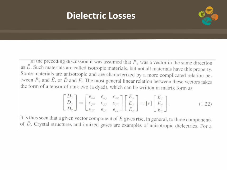
Dielectric Losses
Electric Flux Density Electric Polarizaton (due to the polarization of atoms caused by an applied electric field)

Dielectric Losses
Dielectric Losses

Skin Depth in Conductors
The skin depth, or characteristic depth of penetration, is defined as
δs =1α
=2
ωµσ
12 (7.1)
Fig. 7.1 Skin depth of a conductor
If the wave propagates into a conducting material having finite conductivity σ, the amplitude of the fields decays by an amount e-1 from its initial value or 36.8%, after traveling a distance of one skin depth, e-αz = e-αδs = e-1. For a conducting material, this distance is very small at microwave frequencies and is called the skin depth ‘δs’ of the material.

Problem7.1 Compute the skin depth of aluminium, gold, and silver at frequency of 10 GHz? Conductivity for aluminium, gold, and silver are 3.816 x 10⁷ S/m, 4.098 x 10⁷ S/m, 6.173 x 10⁷ S/m respectively.
Answer: 8.14 x 10⁻⁷ m, 7.86 x 10⁻⁷ m, 6.4 x 10⁻⁷ m

Microstrip Line
Fig. 7.2 Micrsotrip line Cross-section
Basically a conductor trace of width ‘w’ on top of a substrate of thickness ‘h’, with a ground plane underneath.
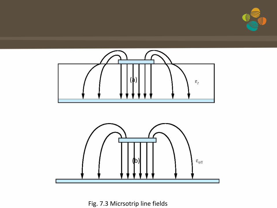
(a) Typical electric field lines in a cross section of microstrip to demonstrate quasi TEM mode. (b) Field lines where the air and dielectric have been replaced by a homogeneous medium of effective relative permittivity εre.
Fig. 7.3 Micrsotrip line fields
(a)
(b)
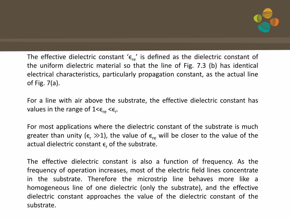
The effective dielectric constant ‘ϵre’ is defined as the dielectric constant of the uniform dielectric material so that the line of Fig. 7.3 (b) has identical electrical characteristics, particularly propagation constant, as the actual line of Fig. 7(a). For a line with air above the substrate, the effective dielectric constant has values in the range of 1<ϵre <ϵr. For most applications where the dielectric constant of the substrate is much greater than unity (ϵr ≫1), the value of ϵre will be closer to the value of the actual dielectric constant ϵr of the substrate. The effective dielectric constant is also a function of frequency. As the frequency of operation increases, most of the electric field lines concentrate in the substrate. Therefore the microstrip line behaves more like a homogeneous line of one dielectric (only the substrate), and the effective dielectric constant approaches the value of the dielectric constant of the substrate.

Design Equations for Microstrip line
In most of the the practical applications, however, the dielectric substrate is electrically very thin (h << λ), and so the fields are quasi TEM. In other words, the fields are essentially the same as those of the static case. Closed-form expressions for Z0 and ϵre when conductor thickness t = 0 are given here
(7.2)
(7.3)
(7.4)

W/h in terms of Z0 and ϵre are as follows:
(7.5)
(7.6)
(7.7)

Microstrip Losses Attenuation in a microstrip structure is caused by two loss components: conductor loss and dielectric loss. Closed-form expressions for the conductor (αc) and dielectric (αd) attenuation constants expressed in decibels per unit length are as follows:
(7.8)
(7.9)
(7.10)

The dielectric loss is normally very small compared with the conductor loss for dielectric substrates such as alumina, etc. The dielectric loss in silicon substrates (used for MMICs), however, is usually of the same order or even larger than the conductor loss. This is because of the lower resistivity available in silicon wafers.
(7.11)
(7.12)

Microstrip Design Equations (Pozar)

15


Determine the dimension ratio W/h and effective dielectric constant of a microstrip line (t=0) of characteristic impedance 50 ohm, printed on a substrate of dielectric constant (εr=2)
Answer: W/h =3.3, εre=1.74
Problem

Calculate the width and length of a microstrip line for a 50 Ω characteristic impedance and a 90 degrees phase shift at 2.5 GHz. The substrate thickness is h= 0.127 cm, with dielectric constant (εr=2.2).
Answer: W/h =3.081, εre=1.87, l= 2.19 cm
Problem

Coplanar Waveguide (CPW) Lines
A conventional CPW on a dielectric substrate consists of a center strip conductor with semi-infinite ground planes on either side as shown in Figure 7.5. This structure supports a quasi-TEM mode of propagation.
Fig. 7.5 CPW cross-section

CPW advantages over conventional microstrip line: First, it simplifies fabrication Second, it facilitates easy shunt as well as series surface mounting of devices Third, it eliminates the need for wraparound and via holes Fourth, it reduces radiation loss Fifth, the characteristic impedance is determined by the ratio of a/b, so size reduction is possible with more degrees of flexibility, Sixth, a ground plane exists between any two adjacent lines, hence cross talk effects are very week, as a result, CPW circuits can be made denser than microstrip circuits. The only penalty being slightly higher losses
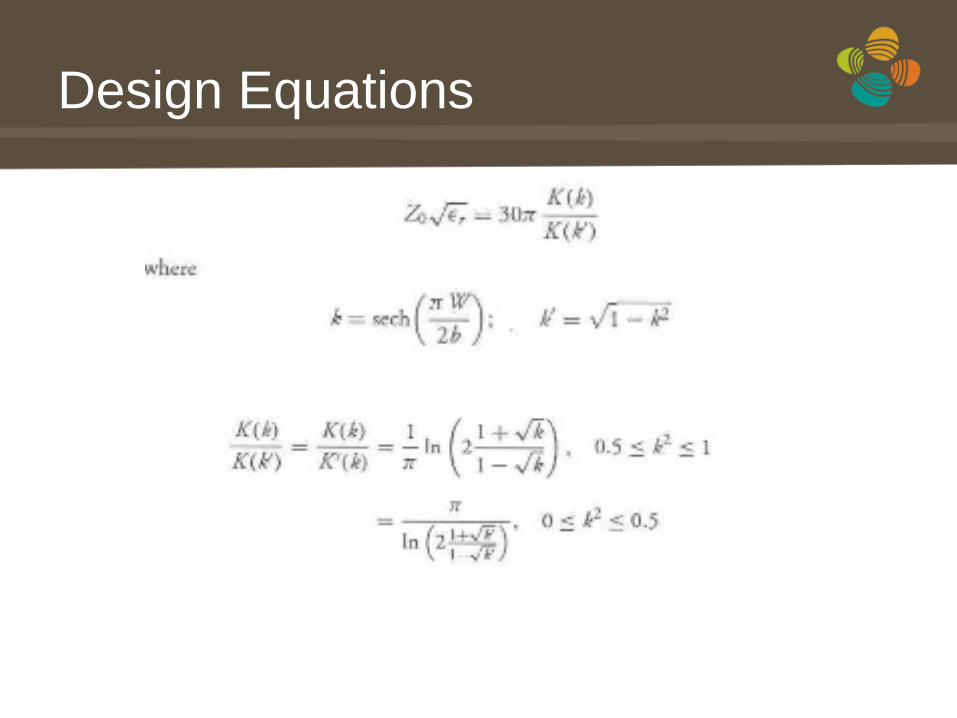
CPW Design Equations
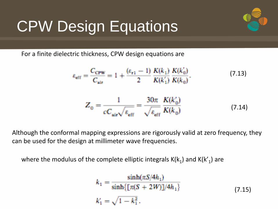
where the modulus of the complete elliptic integrals K(k1) and K(k’1) are
For a finite dielectric thickness, CPW design equations are
Although the conformal mapping expressions are rigorously valid at zero frequency, they can be used for the design at millimeter wave frequencies.
(7.14)
(7.13)
(7.15)
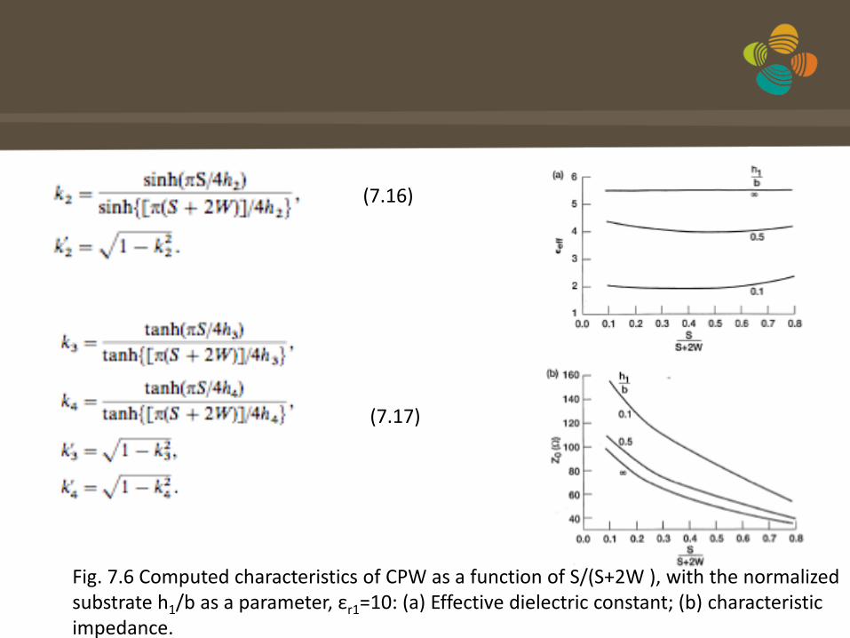
Fig. 7.6 Computed characteristics of CPW as a function of S/(S+2W ), with the normalized substrate h1/b as a parameter, εr1=10: (a) Effective dielectric constant; (b) characteristic impedance.
(7.16)
(7.17)

Stripline
Fig. 7.7 Stripline Cross-section
The stripline, shown in Fig. 7.7, has the conductor sandwiched between two flat dielectric substrates having the same dielectric constant. The outer surface of the dielectric substrates are metalized and serve as ground conductors. The signal is applied between the strip conductor and the ground. The thickness of both the substrates (top and bottom) are generally the same, however it is not necessary. A stripline can support a pure TEM mode
Design Equations

Alternate Design Equations (Pozar)


Coplanar strips (CPS)
It is realized by setting two conductor strips of width “w 1 ” and “w 2 ” in close proximity supported by a dielectric of thickness “h.” Note that on the other side of the dielectric there is no ground plane. “CPS” can be regarded as the complement of the “CPW” since conductors are present where they are absent in “CPW.” Typically used to feed differential antennas like dipole and loop.

Transitions
It may be required to interface one type of transmission line to another in a microwave system, either for measurement purposes or for overall system design. This requires careful design of transition between the two types of transmission lines. For example, it is typical to use coaxial connections below 5 GHz and waveguides above 20 GHz and either type of line in the intermediate frequency range. Some of the typical transitions are shown here.
(a) (b) Fig. 7.8 Coaxial to Microstrip transition (a) Low frequency (b) Medium Frequency range

Fig. 7.10 Microstrip to Coplanar Waveguide transition
Fig. 7.9 Rectangular Waveguide to Microstrip transition