ee143%– fall%2016 microfabrication%technologies …ee143/fa16/lectures/lecture08... · 1 1...
TRANSCRIPT

1
1
EE143 – Fall 2016Microfabrication Technologies
Lecture 8: DiffusionReading: Jaeger Chapter 4
Prof. Ming C. Wu
511 Sutardja Dai Hall (SDH)
2
Surface Diffusion: Dopant Sources(a) Gas Source: AsH3, PH3, B2H6
(b) Solid Source BN Si BN Si
(c) Spin-on-glass SiO2+dopant oxide
(d) Liquid Source.
ceramic wafer of boron nitride

2
3
Fick’s First Law of Diffusion
t coefficiendiffusion =DxNDJ¶¶
-=
4
Fick’s Second Law of Diffusion
devicesmodernin situationsmany in t trueisn'which
t,independen-ionconcentrat is D Assumes
Eqn. Continuity with LawFirst Combine :Diffusion of Law Second sFick'
dimension) one(in
flux particle theof divergence theof negative the toequal ision concentrat of increase of Rate
:Flux Particlefor Equation Continuity
2
2
xND
tN
xJ
tN
¶¶
¶¶
¶¶
¶¶
=
-=

3
5
B,P
As
Au
Cu
kTE
O
A
eDD-
=
Diffusion Coefficients of Impurities in Si
SubstitutionalDiffusers Interstitial
Diffusers
6
Diffusion Coefficients
re temperatuabsolute=TJ/K x101.38=constant sBoltzmann'=k
energy activationE
ipRelationsh Arrhenius exp
23-A =
÷øö
çèæ-=kTEDD A
O

4
7
(a) Interstitial Diffusion
Diffusion Mechanisms in Si
10-6 cm2/secAu
Cu
Fast DiffusionExample: Cu, Fe, Li, H
8
(b) Substitutional Diffusion
Diffusion Mechanisms in Si
(c) Interstitialcy DiffusionExample: Dopants in Si ( e.g. B, P,As,Sb)
5
9
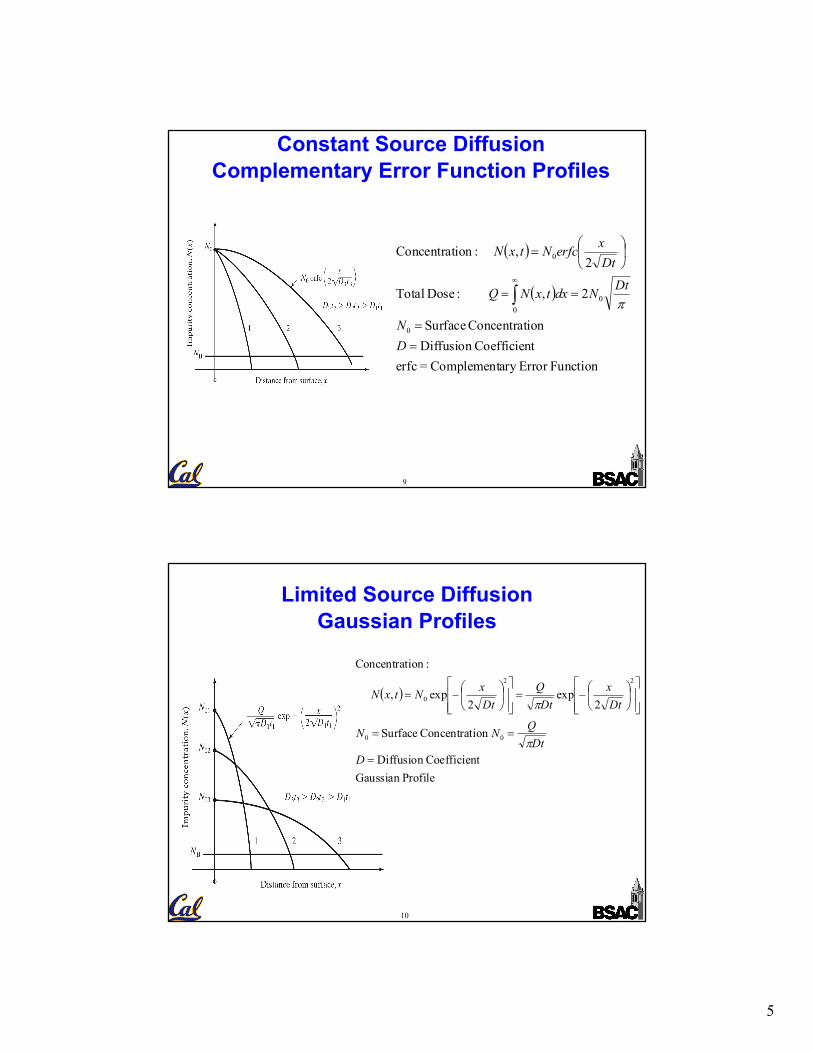
Constant Source DiffusionComplementary Error Function Profiles
( )
( )
FunctionError ary Complement=erfctCoefficienDiffusion
ionConcentrat Surface
2, :Dose Total
2, :ionConcentrat
0
00
0
==
==
÷ø
öçè
æ=
ò¥
DN
DtNdxtxNQ
DtxerfcNtxN
p
10
Limited Source DiffusionGaussian Profiles
( )
ProfileGaussian tCoefficienDiffusion
ion Concentrat Surface
2exp
2exp,
:ionConcentrat
00
22
0
=
==
úúû
ù
êêë
é÷ø
öçè
æ-=úúû
ù
êêë
é÷ø
öçè
æ-=
DDtQNN
Dtx
DtQ
DtxNtxN
p
p
6
11
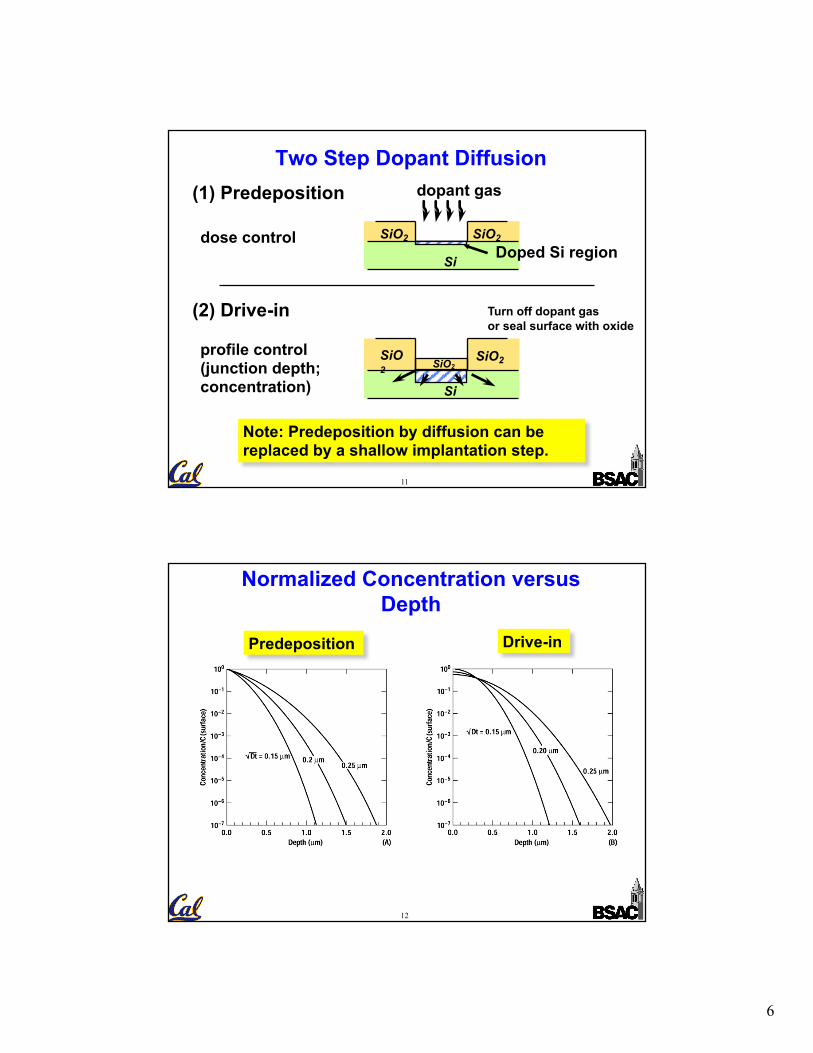
Two Step Dopant Diffusion (1) Predeposition dopant gas
SiO2SiO2
Si
dose control
(2) Drive-in Turn off dopant gasor seal surface with oxide
SiO2SiO2
Si
SiO2
Doped Si region
profile control(junction depth;;concentration)
Note: Predeposition by diffusion can be replaced by a shallow implantation step.
12
Predeposition Drive-in
Normalized Concentration versus Depth

7
13
Diffusion of Gaussian Implantation Profile
14
å=istep
ieffective DtDtBudgetThermal
)()(
Example: Dttotal for Well drive-in and S/D annealing
Temp
time
welldrive-instep
S/DAnnealstep
Temp
time
welldrive-instep
S/DAnnealstep
For a complete process flow, only those steps with high Dt values are important
Successive Diffusions: Thermal Budget

8
15
Solid Solubility Limits
• There is a limit to the amount of a given impurity that can be “dissolved” in silicon (the Solid Solubility Limit)
• At high concentrations, all of the impurities introduced into silicon will not be electrically active
16
High Concentration Diffusion Effects
Log C(x)
x
Low conc profile:Erfc or gaussian
Log C(x)
x
J large
J small
High conc. profile:D gets largerwhen C(x) is large
* C(x) looks “flatter”at high conc. regions
1) E-Field Enhanced Diffusion2) Charged point defects enhanced diffusion
9
17
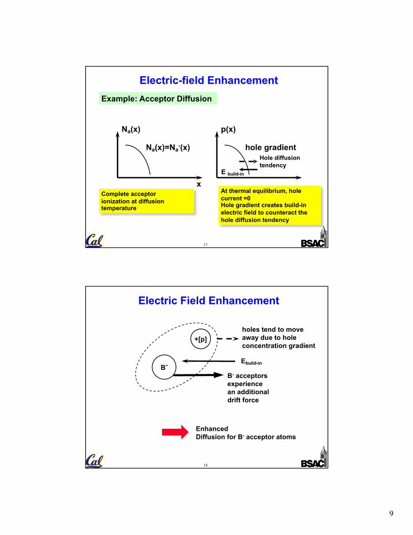
Electric-field EnhancementExample: Acceptor Diffusion
Na(x)
Na(x)=Na-(x)
p(x)
hole gradient
x
Hole diffusion tendency
E build-in
Complete acceptorionization at diffusion temperature
At thermal equilibrium, hole current =0Hole gradient creates build-inelectric field to counteract the hole diffusion tendency
18
B-
+[p]holes tend to moveaway due to holeconcentration gradient
Ebuild-in
B- acceptorsexperiencean additionaldrift force
Enhanced Diffusion for B- acceptor atoms
Electric Field Enhancement

10
19
Asdiffusion
Uniform B conc in substrate
caused by Asconc gradient
B-
Electric Field Enhancement – Substrate Perturbation
20
Example : High Concentration Arsenic diffusion profile becomes “box-like”
11
21
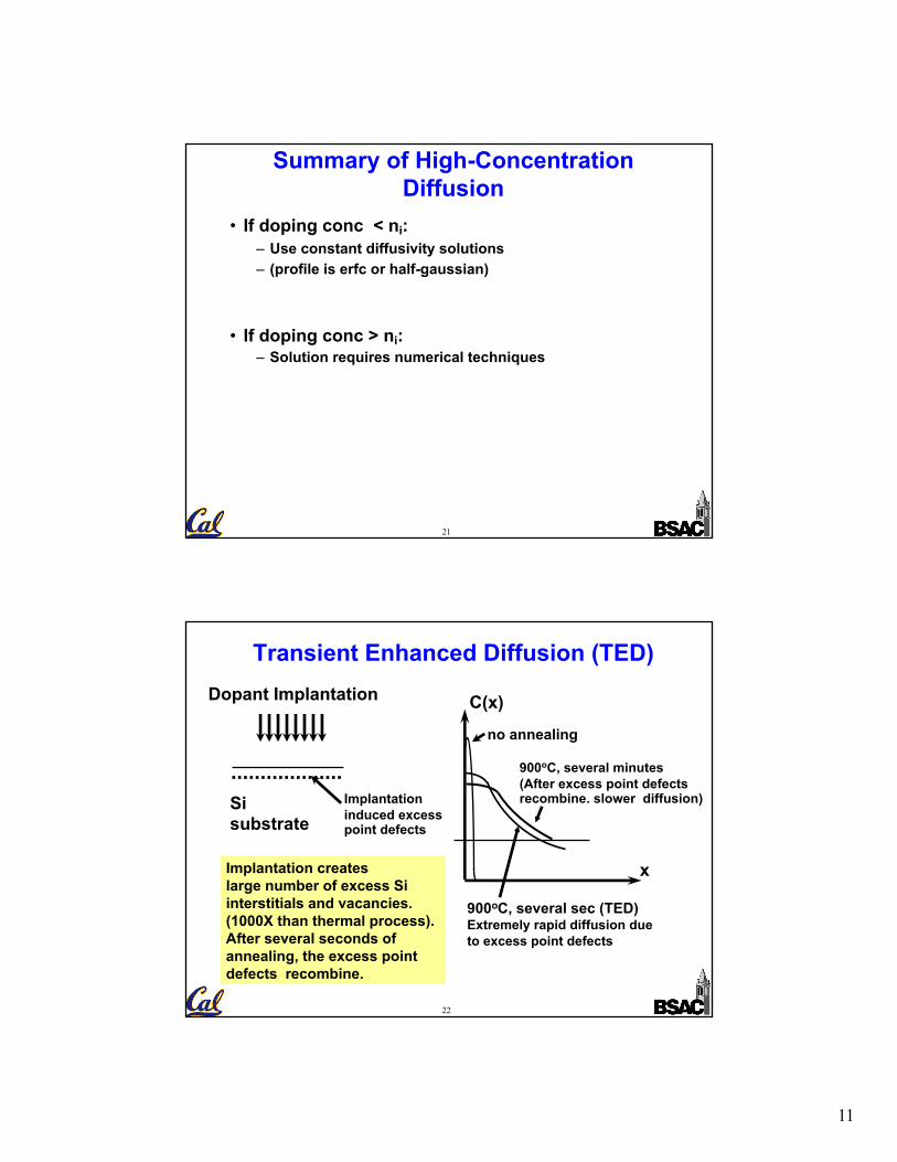
Summary of High-Concentration Diffusion
• If doping conc < ni:– Use constant diffusivity solutions– (profile is erfc or half-gaussian)
• If doping conc > ni:– Solution requires numerical techniques
22
Transient Enhanced Diffusion (TED)Dopant Implantation
Sisubstrate
Implantationinduced excesspoint defects
x
C(x)no annealing
900oC, several sec (TED)Extremely rapid diffusion due to excess point defects
Implantation createslarge number of excess Siinterstitials and vacancies.(1000X than thermal process).After several seconds of annealing, the excess point defects recombine.
900oC, several minutes(After excess point defects recombine. slower diffusion)
12
23
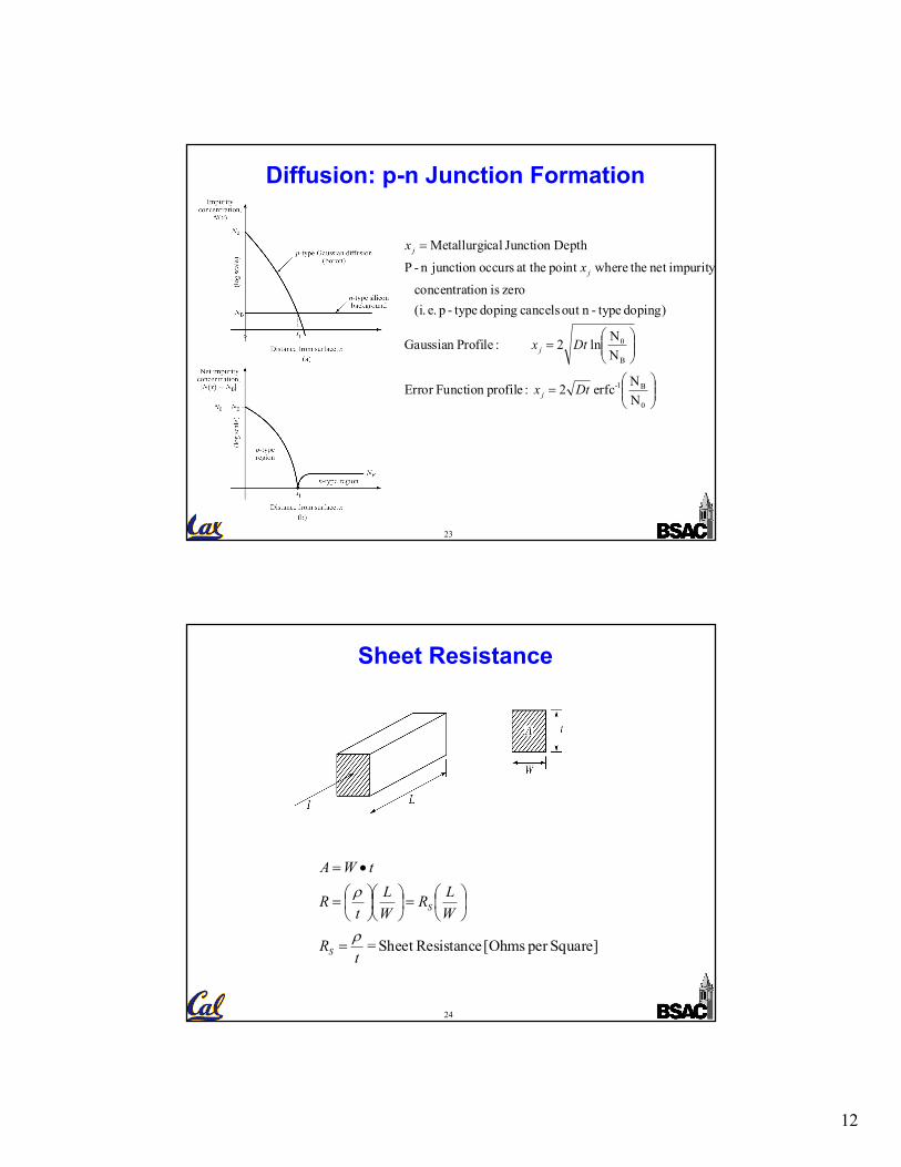
Diffusion: p-n Junction Formation
÷÷ø
öççè
æ=
÷÷ø
öççè
æ=
=
0
B1-
B
0
NNerfc 2 :profileFunction Error
NNln 2 :ProfileGaussian
doping) type-nout cancels doping type-p e. (i. zero ision concentrat
impuritynet the wherepoint at the occursjunction n -P
DepthJunction calMetallurgi
Dtx
Dtx
xx
j
j
j
j
24
Sheet Resistance
Square]per [Ohms ResistanceSheet =t
R
WLR
WL
tR
tWA
S
S
r
r
=
÷øö
çèæ=÷
øö
çèæ÷øö
çèæ=
•=

13
25
Resistivity vs. Doping
r =s-1 = q µnn + µp p( )[ ]-1
n- type : r @ qµn ND -NA( )[ ]-1
p- type : r @ qµp NA -ND( )[ ]-1
26
Resistivity Measurement: Four-Point Probe
tMeasuremen Resistance TerminalFour
/square][ 53.42ln
t>> sfor m]-[ 2ln
s>>for t m]-[ 2
W@==
W=
W=
IV
IV
tR
IVtIVs
Spr
pr
pr

14
27
Impurity Profiling withSecondary Ion Mass Spectroscopy (SIMS)