ee 308/meng 483 spring 2017 - electrical engineering …erives/308_17/exam2_review_s17.pdfee...
TRANSCRIPT

EE 308/MENG 483 Spring 2017
Exam II Review April 2017
Introduction to the MC9S12 Timer Subsystem
The MC9S12 has a 16-bit counter that runs with a 24 MHz.
The clock starts at 0x0000, counts up until it gets to 0xFFFF.
It takes 2.7307 ms (65,536 counts/24,000,000 counts/sec) for the counter to count from 0x0000 to 0xFFFF and roll over to 0x0000.
Registers used to enable Timer Overflow

EE 308/MENG 483 Spring 2017
Code needed to use the timer overflow:
...asm(sei); /* Disable interrupts */TSCR1 = 0x80; /* Turn on timer */TSCR2 = 0x85; /* Enable timer overflow interrupt, set */
/* prescaler */TFLG2 = 0x80; /* Clear timer interrupt flag */UserTimerOvf = (unsigned short)&toi_isr;
asm(cli); /* Enable interrupts (clear I bit) */while (1){
/* Put code here to do things */}...
void interrupt toi_isr(void){
...TFLG2 = 0x80; /* Clear timer interrupt flag */
}

EE 308/MENG 483 Spring 2017
By setting prescaler bits PR2,PR1,PR0 of TSCR2 you can slow down the clock:
PR Divide Freq Overflow Rate000 1 24 MHz 2.7307 ms001 2 12 MHz 5.4613 ms010 4 6 MHz 10.9227 ms011 8 3 MHz 21.8453 ms100 16 1.5 MHz 43.6907 ms101 32 0.75 MHz 87.3813 ms110 64 0.375 MHz 174.7627 ms111 128 0.1875 MHz 349.5253 ms
Interrupt vectors for the HCS12
The interrupt vectors for the MC9S12DP256 are located in memory from 0xFF80 to 0xFFFF.
These vectors are programmed into Flash EEPROM and are very difficult to change
DBug12 redirects the interrupts to a region of RAM where they areeasy to change
For example, when the MC9S12 gets a TOF interrupt:
– It loads the PC with the contents of 0xFFDE and 0xFFDF.
– The program at that address tells the MC9S12 to look at address 0x3E5E and 0x3E5F.

EE 308/MENG 483 Spring 2017
For C programs, the vectors are defined in the file vectors12.h. Here is the define statement for the TOF:
#define UserTimerOvf _VEC16(47) /* Maps to 0x3E5E */

EE 308/MENG 483 Spring 2017
EE 308/MENG 483 Spring 2017
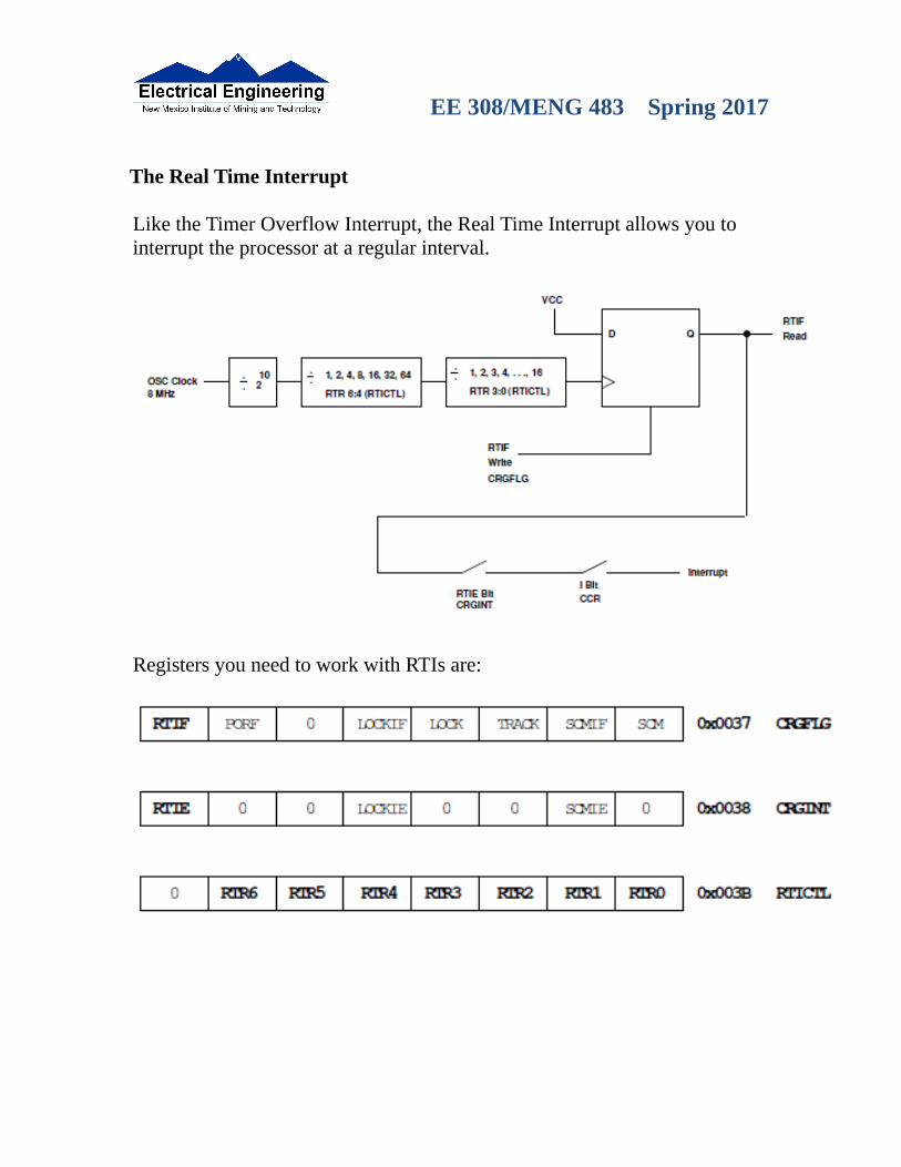
The Real Time Interrupt
Like the Timer Overflow Interrupt, the Real Time Interrupt allows you to interrupt the processor at a regular interval.
Registers you need to work with RTIs are:

EE 308/MENG 483 Spring 2017
The following table shows all possible values, in ms, selectable by the RTICTL register (assuming a 8 MHz oscillator):
Code needed to use the real time interrupt
...asm(sei); /* Disable interruptsRTICTL = 0x63; /* Set rate to 16.384 ms */CRGINT = 0x80; /* Enable RTI interrupts */CRGFLG = 0x80; /* Clear RTI Flag */UserRTI = (unsigned short) &rti_isr;asm(cli); /* Enable interrupts */
while (1){
_ _asm(wai); /* Do nothing -- wait for interrupt */}

EE 308/MENG 483 Spring 2017
interrupt void rti_isr(void){
...CRGFLG = 0x80;
}
The MC9S12 Input Capture Function

EE 308/MENG 483 Spring 2017
Registers used to enable Input Capture Function
Write a 1 to Bit 7 of TSCR1 to turn on timer
Set the prescaler in TSCR2
Write a 0 to the bits of TIOS to make those pins input capture

EE 308/MENG 483 Spring 2017
Write to TCTL3 and TCTL4 to choose edge(s) to capture
To clear the flag, write a 1 to the bit you want to clear
To enable interrupt when specified edge occurs, set corresponding bit in TIE register
To determine time of specified edge, read 16−bit result registers TC0 thru TC7

EE 308/MENG 483 Spring 2017
Consider to wait until an event occurs on Pin 2 of PTT:
...asm(sei);done = FALSE;
/* Turn on timer subsystem */TSCR1 = 0x80;
/* Set prescaler to 32 (87.38 ms), no TOF interrupt */TSCR2 = 0x05;
/* Setup for IC1 */TIOS = TIOS & ~0x02; /* Configure PT1 as IC */TCTL4 = (TCTL4 | 0x04) & ~0x08; /* Capture Rising Edge */TFLG1 = 0x02; /* Clear IC1 Flag */UserTimerCh1 = (short) &tic1_isr;TIE = TIE | 0x02; /* Enable IC1 Interrupt */
/* Setup for IC2 */TIOS = TIOS & ~0x04; /* Configure PT2 as IC */TCTL4 = (TCTL4 | 0x10) & ~0x20; /* Capture Rising Edge */TFLG1 = 0x04; /* Clear IC2 Flag */UserTimerCh2 = (short) &tic2_isr;TIE = TIE | 0x04; /* Enable IC2 Interrupt */
/* Enable interrupts by clearing I bit of CCR */asm(cli);while (!done){
asm(wai); /* Low power mode while waiting */}time = second - first; /* Calculate total time */...

EE 308/MENG 483 Spring 2017
interrupt void tic1_isr(void){
first = TC1;TFLG1 = 0x02;
}
interrupt void tic2_isr(void){
second = TC2;done = TRUE;TFLG1 = 0x04;
}
The MC9S12 Output Compare Function
EE 308/MENG 483 Spring 2017
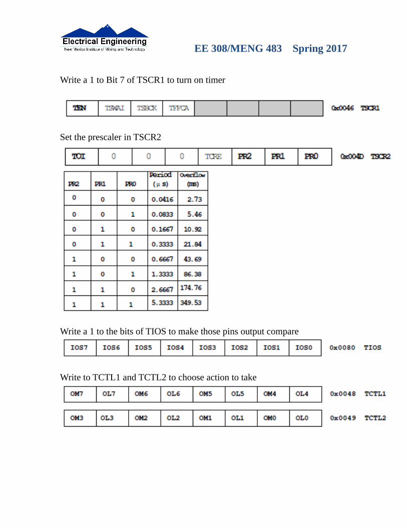
Write a 1 to Bit 7 of TSCR1 to turn on timer
Set the prescaler in TSCR2
Write a 1 to the bits of TIOS to make those pins output compare
Write to TCTL1 and TCTL2 to choose action to take

EE 308/MENG 483 Spring 2017
Write time you want event to occur to TCn register. To have next event occur T cycles after last event, add T to TCn.
To clear the flag, write a 1 to the bit you want to clear (0 to all others)
To enable interrupt when compare occurs, set corresponding bit in TIE register
Program to implement a 100 Hz square wave on output pin PT2: Make output toggle ever 5 ms, for a 10 ms period: 5 ms * 24 × 106 cycles/s = 120, 000 cycles. TCNT can only count up to 65,536 cycles. Need to use prescaler to get correct frequency. A prescaler of 4 divides the clock by 16, so: 5 ms * (24 × 106 cycles/s / 16) = 7, 500 cycles.
...#define PERIOD 15000#define HALF_PERIOD (PERIOD/2)...
asm(sei); /* disable interrupts */TSCR1 = 0x80; /* Turn on timer subsystem */TSCR2 = 0x04; /* Set prescaler to 0.666 us */TIOS = TIOS | 0x04; /* PT2 as Output Compare */TCTL2 = (TCTL2 | 0x10) & ~0x20; /* to toggle on compare */TFLG1 = 0x04; /* Clear Channel 2 flag */

EE 308/MENG 483 Spring 2017
UserTimerCh2 = (unsigned short) &toc2_isr;TIE = TIE | 0x04; /* Enable interrupt on Channel 2*/asm(cli); /* global enable */
while (1){
_ _asm(wai);} ...
interrupt void toc2_isr(void){
TC2 = TC2 + HALF_PERIOD;TFLG1 = 0x04;
}
Pulse Width Modulation on the MC9S12
Because PWM is used so often the MC9S12 has a built-in PWM system.
The MC9S12 PWM does not use interrupts.
The PWM system on the MC9S12 is very flexible.
To enable the PWM output on one of the pins of Port P, write a 1 to the appropriate bit of PWME
PWMPOLn − Choose polarity 1 => high polarity 0 => low polarityWe will use high polarity only. PWMPOL = 0xFF;
PWMCLKn − Choose clock source for Channel n

EE 308/MENG 483 Spring 2017
CH5, CH4, CH1, CH0 can use either A (0) or SA (1)CH7, CH6, CH3, CH2 can use either B (0) or SB (1)
This register selects the prescale clock source for clocks A and B independently
Select center aligned outputs (1) or left aligned outputs (0)
Choose PWMCTL = 0x00 to choose 8−bit mode
PWMSCLA adjusts frequency of Clock SA
PWMSCLB adjusts frequency of Clock SB
How to set the Period for PWM Channel 0
To get a 0.5 ms PWM period, you need 12,000 cycles of the 24 MHz clock.

EE 308/MENG 483 Spring 2017
PWMPER0 × 2PCKA if PCLK0 == 012, 000=
PWMPER0 × 2PCKA+1 × PWMSCLA if PCLK0 == 1
Code to set up PWM Channel 0 for 0.5 ms period:2 kHz frequency, PWM with 60% duty cycle
PWMCTL = 0x00; /* 8-bit Mode */PWMPOL = 0xFF; /* High polarity mode */PWMCAE = 0x00; /* Left-Aligned */
PWMPRCLK = PWMPRCLK & ~0x07; /* PCKA = 0 */PWMCLK = PWMCLK | 0x01; /* PCLK0 = 1 */PWMSCLA = 30;PWMPER0 = 200;PWME = PWME | 0x01; /* Enable PWM Channel 0 */PWMDTY0 = 120; /* 60% duty cycle on Channel 0 */
MC9S12 Analog/Digital Converter
A 10-bit A/D converter is used to convert an input voltage. The reference voltages are VRL = 0V and VRH = 5V.
– What is the quantization level of the A/D converter?
ΔV = (VRH − VRL)/(2b -1) = 4.88 mV
If the value read from the A/D converter is 0x15A, what is the input voltage?
Vin = VRL + [(VRH − VRL)/(2b-1)]*ADvalue = 0 V + 4.88 mV × 346 = 1.6894 V

EE 308/MENG 483 Spring 2017
To program the HCS12 A/D converter you need to set up the A/D control registers ATD0CTL2, ATD0CTL3, ATD0CTL4 and ATD0CTL5.
The registers needed to use the A/D are:
To Power up A/D Converter (ADPU = 1 in ATD0CTL2)
To Select number of conversions per sequence (S8C S4C S2C S1C in ATD0CTL3)
S8C S4C S2C S1C = 0001 to 0111 for 1 to 7 conversionsS8C S4C S2C S1C = 0000 or 1xxx for 8 conversions
To select 8-bit mode write 0x85 to ATD0CTL4To select 10-bit mode write 0x05 to ATD0CTL4*Other values of ATD0CTL4 either will not work or will result in slower A/D conversion rates
To select:DJM = 0 => Left justified data in the result registersDJM = 1 => Right justified data in the result registers
DSGN = 0 => Unsigned data representation in the result registerDSGN = 1 => Signed data representation in the result register
SCAN = 0: Convert one sequence, then stopSCAN = 1: Convert continuously
MULT = 0: Convert one channel the specified number of times - Choose channel to convert with CC, CB, CA.
MULT = 1: Convert across several channels.- First channel to be converted is CC, CB, CA

EE 308/MENG 483 Spring 2017
After writing to ATD0CTL5, the A/D converter starts, and the SCF bit is cleared. After a sequence of conversions is completed, the SCF flag is set.
You can read the results in ATD0DRx.
To setup the A/D to do 8 conversions, in 8-bit mode, on Channel 4:
...ATD0CTL2 = 0x80; /* Power up A/D, no interrupts */ATD0CTL3 = 0x00; /* Do eight conversions */ATD0CTL4 = 0x85; /* 8-bit mode */ATD0CTL5 = 0xA4; /* 1 0 1 0 0 1 0 0
| | | | \___/ | | | | | | | | | \__ Bit 4 of Port AD | | | \____ MULT = 0 => one channel only | | \___ Scan = 1 => continuous conversion | \_____DSGN = 0 => unsigned \______ DJM = 1 => right justified */