ee 147/247a prof. pister fall 2020 homework assignment #2
TRANSCRIPT

EE 147/247A Prof. Pister Fall 2020
Homework Assignment #2 Rubric
1. [7 pts total] You have a solid cube of aluminum of side length S sitting a distance d beneath a large flat conductive plate, creating a parallel plate gap between them. You apply a voltage V between the cube and the plate, which generates an upwards force on the cube. If d=S/10
a. [1 pt] Does the magnitude of the force depend upon S? 1 point for “no”. It would be nice to see the derivation, but not required.
𝐹 =12 𝜖&𝑉
( 𝐴𝑔( =
12 𝜖&𝑉
( 𝑆 ∗ 𝑆
- 𝑆10/( =
12 𝜖&𝑉
((100)
b. [3 pts] Using the approximation that ½ e0(15V)2=1nN, what is the force on the cube if
V=1.5V, 15V, and 150V? If you used a calculator instead of the approximation, take 1 point off! There should be no more than one significant figure in your answer.
1.5V: 1003(𝜖&(1.5𝑉)( = 1𝑛𝑁
15V: 1003(𝜖&(15𝑉)( = 100𝑛𝑁
150V: 1003(𝜖&(150𝑉)( = 10𝑢𝑁
c. [3 pts] For the three voltages above, calculate the range of values of S for which the mass
of the cube is less than the electrostatic force lifting it up (note: -1 point for me for comparing “the mass of the cube” to a force. I should have said the weight of the cube - ksjp) If you just solved for the value at which the forces are equal, but didn’t give the range of values, subtract 1 point total even if you did it three times. It’s fine if you wrote “or less” or anything that indicates a range.
𝐹9: = 𝑚 ∗ 𝑔 = 𝑉 ∗ 𝑝=> ∗ 𝑔 = 𝑆?(2710) ∗ 10=27100𝑆?𝑁 ≈ 25000𝑆? N
1.5V→ 1𝑛𝑁:𝐹9: < 1𝑛𝑁 𝑆? < 4 ∗ 10F3G𝑚?
S<3.5 ∗ 10FI𝑚
15V→ 100𝑛𝑁:𝐹9: < 100𝑛𝑁 𝑆? < 4 ∗ 10F3(𝑚?
S<1.5 ∗ 10FG𝑚
150V→ 10𝑢𝑁:𝐹9: < 10𝑢𝑁 𝑆? < 4 ∗ 10F3&𝑚?
S<7 ∗ 10FG𝑚
2. [14 pts. total] In a single-mask SOI process in which your minimum lithography line and space is
l, you wish to make an accelerometer with a variable capacitor readout, like our simplest accelerometer (e.g. in lecture W2L2 at around 34 minutes). Two of the many capacitor finger pairs are shown below, showing the desired front gap gf, and the undesired back gap gb.
a. [4 pts] For a displacement of the proof mass over the range y = [-gf, gb], sketch the front gap capacitance, back gap capacitance, and total capacitance assuming gb =10 gf. You

should have some asymptotes! Show clearly the relative front and back capacitance values when y=0.
1 point each for getting the asymptotes right on each curve (3 pts total)
1 point for showing that the back gap is 10 times lower capacitance than front gap at y=0
b. [1 pt] What is the impact of the back gap on dC/dy near y=0? 1 point for stating that the back gap reduces the overall dC/dy, or saying that it has a negative impact.
Don’t need a numerical answer for full credit, but it would be nice.
𝐶(𝑦) = 𝜖&𝑡𝐿(1
𝑔N − 𝑦+
1𝑔Q + 𝑦
)
𝐶R =𝑑𝐶(𝑦)𝑑𝑦 = 𝜖&𝑡𝐿(
1(𝑔N − 𝑦)(
−1
(𝑔Q + 𝑦)()
𝑑𝐶(𝑦)𝑑𝑦
TUV&
= 𝜖&𝑡𝐿(1
(𝑔N)(−
1(𝑔Q)(
)
So when gb=10gf, the magnitude of dC/dy is reduced by only 1%. Clearly we can get a bigger dC/dy signal if we put the fingers closer than this.

c. [5 pts] Repeat parts a and b, assuming gb = gf.
𝐶R =𝑑𝐶(𝑦)𝑑𝑦 = 𝜖&𝑡𝐿(
1(𝑔N − 𝑦)(
−1
(𝑔Q + 𝑦)()
𝑖𝑓𝑔N = 𝑔Q𝑎𝑛𝑑𝑦 = 0, 𝑡ℎ𝑒𝑛𝐶R(0) =𝑑𝐶(0)𝑑𝑦 = 0
Must state that dC/dy=0 to get the last point. Note that dC/dy=0 means that there is no net electrostatic force, and no capacitive signal to detect. So now we’ve definitely put the fingers too close!
Making gb too big means we don’t get very many fingers, so we don’t have much capacitance per layout area, and there is an upper limit on how much area we can use. Making gb too small means that we can put in a lot of fingers, but the change in capacitance per finger gets smaller. Somewhere there is an optimum.
d. [4 pts] Assuming that the width of the capacitor fingers and the front gap is l, what is the value of the back gap that maximizes dC/dy at y=0 per unit layout area? I’ve drawn a representative tile-able layout area in red below.
2 points for writing an equation for dC/dy per layout area (1 point if you wrote an equation for capacitance per area instead)

1 point for taking a derivative with respect to the back gap gb 1 point for getting the right answer
As in part b: ]^(U)
]U= 𝜖&𝑡𝐿(
3(:_FU)`
− 3(:abU)`
)
𝑑𝐶(𝑦)𝑑𝑦
TUV&
= 𝜖&𝑡𝐿(1
(𝑔N)(−
1(𝑔Q)(
)
The Area denoted by the dotted red line is A=L(𝑔N + 𝑔Q + 2𝑤);𝑤ℎ𝑒𝑟𝑒𝑤𝑖𝑠𝑡ℎ𝑒𝑓𝑖𝑛𝑔𝑒𝑟𝑤𝑖𝑑𝑡ℎ
Area Density AD =gh(i)gi j
ikl
=
AD = mlno(
p
qr_sit`F
p(raui)`
)
v(:_b:ab(w)
But 𝑔Q = 𝑤 = 𝜆 so AD = mlno(
p
qr_t`F
py`)
v(:_b?z)
And we can cancel and L before deriving ]={]:_
= mln(:_|F?:_z`F}z|):_|z|(:_b?)`
= 0 𝜖&𝑡(𝑔N? − 3𝑔N𝜆( − 6𝜆?) = 0
The only real root is 𝑔N = 2.35𝜆 As an example, if you have 2 um line and space lithography and you are making a gap-closing actuator or capacitive sensor, you maximize your force or capacitance change per unit area by making the front gap and fingers 2 um wide, and the back gap 4.7 um wide. Note that if the fingers and the front gap are not the same size (sometimes we make the fingers wider to avoid electrostatic pull-in) then the optimal back gap will vary somewhat.
3. [4 pts] For this problem, assume that the fracture strain of silicon is 1%. You may use 50 kg as
your mass if you’d rather not disclose personal information. a. [2pts] What is the minimum cross-sectional area of a silicon wire that will hold your
weight without breaking? 2 points if you get the right answer. 1 point for some explanation and the wrong answer
𝑚 = 50𝑘𝑔 𝐹 = 𝑚𝑔 = 𝑘𝑥=�=
o𝑥 = 𝐸𝐴𝜖 → 𝐴 = �
�m =9:
�m
𝐴 =I&�:∗3&�
�`
3I&���∗&.&3 = 3&
?∗3&�s` = 3 ∗ 10F� 𝑚(
1
y gf
gb
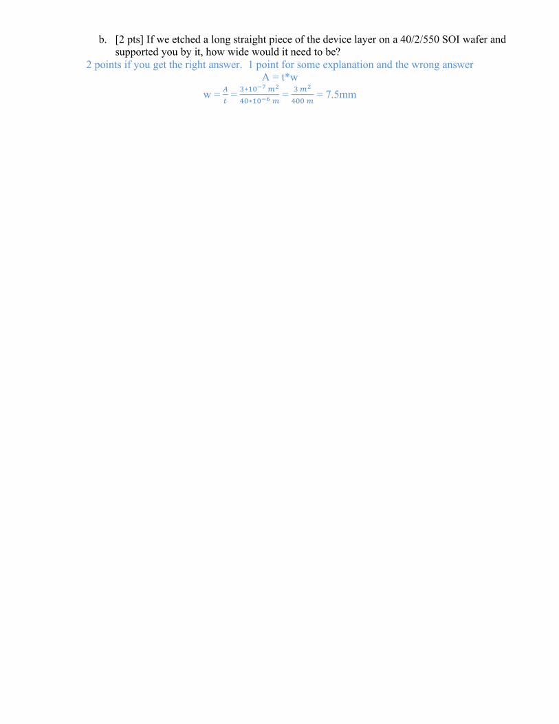
b. [2 pts] If we etched a long straight piece of the device layer on a 40/2/550 SOI wafer and supported you by it, how wide would it need to be?
2 points if you get the right answer. 1 point for some explanation and the wrong answer A = t*w
w = =n = ?∗3&
s�9`
G&∗3&s�9 = ?9
`
G&&9 = 7.5mm