École de technologie supÉrieure …espace.etsmtl.ca/479/1/kincic_slaven_2006.pdf ·...
TRANSCRIPT

Reproduced with permission of the copyright owner. Further reproduction prohibited without permission.
ÉCOLE DE TECHNOLOGIE SUPÉRIEURE
UNIVERSITÉ DU QUÉBEC
A THESIS SUBMITTED TO
ÉCOLE DE TECHNOLOGIE SUPÉRIEURE
IN PARTIAL FULFILLMENT OF THE REQUIREMNTS
FOR THE DEGREE
DOCTOR OF PHILOSOPHY
Ph.D
BY
SLA VEN KINCIC
VOLTAGE SUPPORT OF TRANSMISSION NETWORK FROM DISTRIBUTION
LEVEL
MONTRÉAL, 13 JUNE 2006
© Copyright Slaven Kincic 2006

Reproduced with permission of the copyright owner. Further reproduction prohibited without permission.
CETTE THÈSE A ÉTÉ ÉVALUÉE
PAR UN JURY COMPOSÉ DE:
M. Ambrish Chandra, directeur de thèse Département de génie électrique à l'École de technologie supérieure
M.Boon-Teck Ooi, codirecteur Département de génie électrique à McGill University
M. Pierre Jean Lagacé, président du jury Département de génie électrique à l'École de technologie supérieure
M. Louis A. Dessaint, Département de génie électrique à 1 'École de technologie supérieure
M. Vijay K. Sood, chercheur Hydro-Quebec (IREQ)
ELLE A FAIT L'OBJET D'UNE SOUTENANCE DEVANT JURY ET PUBLIC
LE 12 MAI 2006
À L'ÉCOLE DE TECHNOLOGIE SUPÉRIEURE

Reproduced with permission of the copyright owner. Further reproduction prohibited without permission.
VOLTAGE SUPPORT OF TRANSMISSION NETWORK FROM DISTRIBUTION
LEVEL
Slaven Kincic
ABSTRACT
In this thesis a new concept is proposed and developed. The concept is named "Transmission Lines Voltage Support Decentralization". It is shown that, when transmission lines require sustained voltage support, it is more efficient and economically beneficiai to provide it on distribution level with large number of smaller sized Static V ar Systems (SVS) regulating distribution voltages rather then with fewer large bulk SVS on transmission level regulating transmission voltages.
The benefits of the proposed concept over the traditional voltage support of transmission lines on transmission level with bulk compensators are underlined. The benefits include lower var requirement, lower transformer MV A requirements, possibility of elimination of L TC transformer for load voltage regulation, lower stand by requirements to satisfy N-1 reliability criterion, enhanced reliability and better voltage regulation of distribution buses. These benefits are converted into the dollar value.
The feasibility and reliability of the proposed concept is demonstrated by detailed, dynamic, real time simulations. Simulation studies have shown that the distributed, distribution voltage support units operate harmoniously in recovery after different kinds of the faults including three phase-to-ground faults.

Reproduced with permission of the copyright owner. Further reproduction prohibited without permission.
SUPPORT DE LA TENSION DE TRANSMISSION PAR
DES COMPENSATEURS STATIQUES LOCALISÉS AU NIVEAU
DE LA DISTRIBUTION
Slaven Kincic
RÉSUMÉ
Dans cette thèse, un nouveau concept de support de la tension du réseau électrique est
proposé. Ce concept consiste à remplacer les compensateurs statiques traditionnels par
des compensateurs de plus petite capacité, localisés au niveau de la distribution. Ses
avantages sont mis en évidence. Le concept peut être avantageux surtout dans le cas
d'une planification et d'une construction de nouvelles lignes de transmission.
Traditionnellement, la régulation dynamique de la tension de transmission est effectuée
avec des compensateurs statiques ou des compensateurs synchrones de grande capacité
qui sont installés au niveau de la transmission. Cette étude propose la restructuration de
l'infrastructure destinée à la régulation de la tension de transmission et le transfert des
compensateurs dynamiques du côté de la transmission (haute tension HT) vers le côté de
la distribution (basse tension BT) de façon à ce que les compensateurs agissent seulement
sur la tension au niveau de la distribution. Enfin, pour améliorer la fiabilité du système,
les compensateurs sont répartis en plusieurs unités de petite taille. Il est démontré que ce
concept est bénéfique, et présente des avantages considérables. Ses caractéristiques sont
analysées en régime permanent. La faisabilité et la robustesse dans les régimes
transitoires sont testées au moyen de nombreuses simulations numériques. Les
simulations numériques sont effectuées en temps réel et en temps différé à l'aide du
simulateur Hypersim développé par l'Hydro-Québec. L'avantage du simulateur Hypersim
réside dans le fait que les simulations dynamiques de longue durée peuvent être exécutées

Reproduced with permission of the copyright owner. Further reproduction prohibited without permission.
111
tout en permettant d'analyser à la fois la stabilité transitoire et les phénomènes à long
terme. Un autre avantage de ce simulateur, est la disponibilité des modèles détaillés de
1' ensemble des composantes d'un réseau électrique. L'analyse en régime permanent et
l'analyse conceptuelle sont élaborées en utilisant les diagrammes vectoriels et la théorie
des circuits électriques, notamment les lois de courant et de tension de Kirchhoff. Dans
l'analyse conceptuelle, cette approche est plus appropriée que celle qui utilise les
équations des écoulements de puissance, car les relations entre les courants, les tensions
et les chutes de tension sont linéaires plutôt que quadratiques. De plus, les diagrammes
vectoriels permettent la visualisation entre les tensions et la chute de tension.
Le premier chapitre de cette thèse analyse la problématique envisagée par l'industrie de
1 'électricité à 1 'heure actuelle, notamment le problème d'instabilité de la tension qui est
une conséquence directe des nouvelles tendances dans l'industrie. En bref, cette
problématique consiste en l'insuffisance de la capacité du réseau de transport, la
déréglementation de l'industrie d'électricité ainsi que la qualité de tension fournie. La
solution traditionnelle de ces problèmes se situe dans le support dynamique de tension
localisé au niveau transmission, soit avec des compensateurs synchrones, soit avec des
compensateurs statiques à grande capacité de compensation. D'autre part, de nouvelles
tendances reliées au protocole de Kyoto, c'est-à-dire l'évolution de la conscience
environnementale et le manque de grandes ressources énergétiques, ont forcé les
planificateurs de réseaux à se tourner vers les ressources renouvelables et les réseaux de
production décentralisée. L'intégration des petites sources dans le réseau d'électricité
conventionnel se fait au niveau de la distribution. La génération de 1 'électricité elle-même
peut être effectuée à l'aide de machine synchrones ou asynchrones, dépendamment de la
nature de la source. La génération intégrée dans le réseau d'électricité conventionnel
localisée au niveau de la distribution nécessite un contrôle dynamique de tension
précisément au point de l'intégration de la source dans le réseau, c'est-à-dire au niveau de
la distribution. Nous pouvons affirmer que les réseaux de production décentralisée
nécessitent un contrôle dynamique de tension par des compensateurs décentralisés.

Reproduced with permission of the copyright owner. Further reproduction prohibited without permission.
iv
Dans ce contexte, il est justifiable d'examiner si le support de tension du réseau entier
peut être effectué par des compensateurs statiques de petite capacité localisés au niveau
de la distribution, sans contrôler directement la tension de transmission. Cette opération
est-elle réalisable, économiquement justifiable et fiable? Serait-il plus bénéfique de
fournir le support de tension par un large compensateur du côté transmission ou de fournir
le support de tension par plusieurs petites unités du côté distribution ? Voici les grands
enjeux qui sont explorés dans cette thèse.
Les causes de la chute de tension et l'action pour y remédier sont analysés dans le
deuxième chapitre. Le courant alternatif, en passant par des lignes de transmission,
produit le champ magnétique qui varie en fonction du temps. Dû à l'inductance de ligne,
et en accord avec la loi de Farady-Lenz, la chute de tension est induite le long de la ligne
de transport. L'action pour remédier à la chute de tension dite inductive consiste à injecter
un courant (appelé le courant de compensation), qui induit la tension égale mais de signe
opposé, en annulant la chute de tension inductive ce qui produit, en effet, le support de
tension. À la fin du chapitre, il est démontré qu'en utilisant le principe de superposition,
c'est-à-dire en fournissant le support de tension du côté distribution, la tension de
transmission est supportée, et vice-versa.
Le troisième chapitre aborde les principes de fonctionnement d'un convertisseur basé sur
les semi-conducteurs et son application comme source de puissance réactive. Un onduleur
à niveaux multiples de topologie calé par diodes est présenté conjointement avec une
commande à fréquence fondamentale (FFM). C'est une configuration attrayante pour des
applications de haute tension, et surtout en tant que ST ATCOM. La commande à
fréquence fondamentale appliquée avec cette configuration minimise les pertes et permet
l'optimisation de forme d'onde de tension produite par le convertisseur. En effet, le
convertisseur, avec l'action rapide des interrupteurs, forme une tension alternative, quasi
sinusoïdale à partir de la tension continue du côté CC du convertisseur. La loi de

Reproduced with permission of the copyright owner. Further reproduction prohibited without permission.
v
commande permettant l'application du convertisseur en tant que compensateur
(STATCOM) est alors conçue et testée.
Dans le chapitre quatre, il est démontré que la stratégie d'utiliser plusieurs compensateurs
de petite taille pour le support de tension du côté distribution présente plus d'avantages
que celle d'utiliser un compensateur de large taille du côté transmission. Les avantages
incluent i) la diminution de réserve afm d'assurer la fiabilité ii) l'élimination du
transformateur élévateur pour couplage de compensateur avec le réseau et, iii) la
diminution de la capacité du compensateur pour assurer le support de la tension. L'étude,
réalisée à 1' aide de la simulation, a été effectuée sur un système test à l'aide du simulateur
Hypersim. Le système test consiste en une ligne radiale de longueur de 300 km et de
315 k V. La puissance maximale transmise à travers la ligne est de 3 7 5 MW. Le support
de tension est effectué au niveau de la distribution à l'aide de quatre compensateurs
(ST ATCOM). Il est démontré que la perte d'un compensateur n'affecte pas le système. Par
contre, si le support de tension est fourni par un compensateur du côté transmission, la
perte du compensateur mène à l'effondrement de la tension. La simulation a démontré
aussi que plusieurs compensateurs dynamiques (STATCOM) fonctionnent en
synchronisme sans interactions néfastes lors des phénomènes transitoires.
Le chapitre cinq constitue une étude détaillée du concept proposé. Deux schémas sont
comparés - le schéma traditionnel, c'est-à-dire la régulation dynamique localisée au
niveau de la transmission par un compensateur de grande capacité versus le schéma
proposé, la régulation dynamique de la tension au niveau de la distribution par plusieurs
compensateurs de petite capacité. Un système général consistant en K lignes de
transmission, fournissant N charges à travers N sous-stations reliées en parallèle, est
considéré. Les lignes de transport sont modélisées à l'aide des paramètres distribués. Les
diagrammes vectoriels sont utilisés pour démontrer la faisabilité et la fiabilité. Par la
suite, les équations permettant le calcul de la puissance nominale du compensateur sont

Reproduced with permission of the copyright owner. Further reproduction prohibited without permission.
VI
déduites en présentant deux cas d'étude: le premier étant un compensateur localisé au
niveau de la distribution, et le second, un compensateur localisé au niveau de la
transmission. Le calcul en p.u. est utilisé. Les équations déduites sont générales, et offrent
une application à tous les niveaux de tension sur différentes longueurs de lignes. À partir
des équations déduites, la puissance nominale en vars est comparée dans deux schémas de
support de tension. La comparaison est effectuée entre différentes longueurs de ligne et
différentes puissances maximales transmises à travers la ligne. L'étude a démontré que,
dans la majorité des cas, le positionnement de la compensation au niveau de la
distribution présente plus d'avantages par rapport au positionnement localisé au niveau de
la transmission en termes de vars requis pour le support de tension. Les avantages sont
convertis en valeur approximative de dollars. Les pertes dues à la résistance de lignes sont
comparées dans deux schémas de compensation. Il est montré qu'en général, les pertes
sont en général moindres pour la compensation du côté distribution. Finalement, un
système de test est étudié à l'aide d'une simulation dynamique.
Dans le chapitre six, les équations générales permettant le calcul du besoin réactif du
réseau nécessaire pour la régulation de tension sont déduites à partir des diagrammes
vectoriels. Les équations sont générales et applicables à 1' ensemble de la distribution des
compensateurs et à toutes les topologies du réseau. La validité des équations est
confirmée avec trois méthodes indépendantes. L'avantage des équations déduites par
rapport aux équations de l'écoulement de puissance réside dans le fait que les besoins
réactifs des compensateurs peuvent être calculés explicitement dans le cas de la
compensation localisée au niveau de la transmission. Le deuxième avantage de ces
équations est que celles-ci permettent l'observation de la proximité du point
d'effondrement de la tension.
L'obje<(tif du chapitre sept est de surmonter l'écart entre le secteur de transmission et de
distribution dans la planification du réseau électrique ainsi que la régulation de tension de

Reproduced with permission of the copyright owner. Further reproduction prohibited without permission.
VIl
transmission et parallèlement, de mettre en évidence le concept avancé, notamment la
décentralisation de la régulation de tension de transmission et son transfert du niveau de
la transmission vers le niveau de la distribution. L'analyse portera sur une ligne radiale de
400 km de longueur et de 230 kV de tension nominale, fournissant 800 MW aux quatre
centres situés le long de la ligne. Le système radial a été retenu pour cette étude, car les
lignes radiales sont les plus vulnérables et les moins fiables. Présentement, une multitude
de lignes radiales sont en service à travers le monde, et ces lignes exigent une régulation
dynamique de la tension, d'où l'importance de cet exercice. De plus, les lignes radiales
seront aussi utilisées afin de permettre l'électrification des communautés éloignées dans
les pays du tiers monde aussi bien que dans les pays de grande superficie. La tension de la
ligne est réglée dynamiquement par quatre compensateurs statiques de var (SVC) du côté
distribution. La stabilité et la robustesse du concept proposé, en prenant en considération
les différentes conditions de charge ainsi que certaines failles, sont démontrées à l'aide de
la simulation numérique.
Finalement, les conclusions ainsi que les recommandations pour les travaux futurs sont
présentées dans le chapitre huit. Les conclusions suivantes sont déduites, à partir du
matériel présenté dans ce document:
1. La régulation dynamique et le support de tension du réseau de transmission
peuvent être effectués d'une façon plus économique du côté distribution sans le
contrôle direct de la tension de transmission.
2. Lorsque la tension de distribution est réglée dynamiquement, la qualité de tension
fournie aux consommateurs est améliorée, et la possibilité d'effondrement de
tension due à la dynamique de moteur à induction s'en trouve diminuée.
3. Si la tension de distribution est contrôlée directement, le transformateur changeur
de prises n'est pas requis, par conséquent le coût du maintien est diminué.
4. Les compensateurs statiques installés 4u côté distribution peuvent être branchés
directement. Le transformateur él~vateur pour le couplage avec le réseau n'est pas

Reproduced with permission of the copyright owner. Further reproduction prohibited without permission.
Vlll
nécessaire, ce qui diminue le coût de compensation d'environ 20 %.
5. L'élimination du transformateur élévateur contribue à la fiabilité du réseau.
6. Si la compensation est effectuée avec plusieurs compensateurs installés du côté
distribution, la perte d'un compensateur n'affectera pas le réseau de façon
considérable. Par contre, si la compensation est effectuée avec un compensateur
du côté transmission, la perte du compensateur pourra mener à l'effondrement de
la tension.
7. Les pertes Joule sont, en général, diminuées si la compensation se fait du côté
distribution.
8. La quantité de puissance réactive requise pour le support de tension du côté
distribution est diminuée par rapport à celui effectué du côté transmission.
9. Le support de tension d'une ligne longue peut être effectué efficacement et
économiquement du côté distribution.
Finalement, dans le cas des réseaux électriques de type radial constitués de très longues
lignes de transport (de longueur 400 km et plus), les compensateurs statiques localisés au
niveau de la transmission jouent un rôle important au niveau de la stabilité transitoire et
des petits signaux. Les compensateurs statiques localisés au niveau de la distribution
peuvent probablement assumer ce rôle en les remplaçant, mais cette thèse n'analyse que le
problème d'effondrement et de support de la tension. En effet, l'aspect de la stabilité
transitoire, ainsi que l'amortissement des oscillations électromécaniques n'est pas abordé
dans cette étude et il représente une recommandation pour le travail futur.

Reproduced with permission of the copyright owner. Further reproduction prohibited without permission.
ACKNOWLEDGMENTS
The thesis represents a fraction of the work that bas been completed in the period between
2001 and 2004. The thesis is the compilation of sorne six conference papers that have
been reviewed and presented in 2002 and 2003 on conferences in Halifax (LESCOPE
2002), Dubrovnik (EPE-PEMC 2002), Lisbon (IEEE Mediterranean Conference on
control Automation), Montreal (CCECE 2003 and LESCOPE 2003) and Toronto
(PES2003 ) together with journal papers that bas been published or accepted for
publication in IEEE Transaction on Power Delivery and lEE Proceedings on Generation,
Transmission and Distribution.
The number of the people have helped me to complete this work and I want to thank to ali
of them.
First of ali I want to express my deepest gratitude to my director Dr. Ambrish Chandra for
the continuous support, funding, encouragement, time and confidence he gave to me. I
have completed my master thesis under his direction too.
I want to express my deepest gratitude to Dr. Boon-Teck Ooi. I have been privileged to
work under his close guidance and supervision. It was an illuminating and motivating
experience. He bas shown me how to fly through time and space as electromagnetic
waves. He was the excitation and control circuit I generated under.

Reproduced with permission of the copyright owner. Further reproduction prohibited without permission.
x
1 want to express my deepest gratitude to Prof. Donald McGillis for his help and
contribution. He has shared a part of his experience and time unselfishly with me.
1 also want to thank to Dr. Z. Huang for his help with Hypersim and his friendship.
1 would like to acknowledge to Ecole de technologie supérieure for providing me three
fellowships (bourse aux mérités) for 2001, 2002 and 2003 and for giving me an
opportunity to lecture different undergraduate and graduate courses.
Finally, special thanks go to my wife for her support and sharing her time with me
throughout this research, before and a:fter.

Reproduced with permission of the copyright owner. Further reproduction prohibited without permission.
TABLE OF CONTENTS
Page
ABSTRACT ......................................................................................................................... i
RESUME ............................................................................................................................ ii
ACKNOWLEDGMENTS ................................................................................................. ix
TABLE OF CONTENTS ................................................................................................... xi
LIST OF FIGURES ......................................................................................................... xvi
LIST OF TABLES ......................................................................................................... xxiv
LIST OF SYMBOLS ...................................................................................................... xxv
CHAPTER 1 1.1 1.2
1.2.1 1.2.2 1.2.3 1.2.4
1.3 1.3.1 1.3.2 1.3.3 1.3.4 1.3.5
1.4 1.5 1.6
CHAPTER2 2.1 2.2 2.3 2.4
2.4.1 2.5
2.5.1 2.5.2 2.5.3 2.5.4
2.6
INTRODUCTION ............................................................................ 1 Voltage Regulation ........................................................................... 2 Needs for Dynamic Voltage Regulation ........................................... 3 Fault Clearing ................................................................................... 3 Wind Farms ...................................................................................... 3 Induction Mo tors .............................................................................. 4 Prevention of Overvoltages .............................................................. 4 State of Art Deviees .......................................................................... 5 Reactive Power Management ........................................................... 5 Shunt F ACTS Controllers ................................................................ 6 Static V ar Systems ............................................................................ 8 Positioning of SVS ........................................................................... 8 Distribution Level SVS .................................................................... 9 Research Objectives ....................................................................... 1 0 Research T ools ............................................................................... 11 Outline of Thesis ............................................................................ 11
VOLTAGE DROP ANALYSIS ..................................................... 13 Introduction .................................................................................... 13 Phenomenology of Power Transfer ................................................ 13 Phase Shift ...................................................................................... 23 Nature ofVoltage Boost ................................................................. 25 Phasor Approach ............................................................................ 26 Voltage Drop Analysis ................................................................... 28 Equivalent Circuit ........................................................................... 28 Non-Compensated Line .................................................................. 29 Power Factor Correction ................................................................. 30 Voltage Regulation ......................................................................... 31 Conclusion ...................................................................................... 35

Reproduced with permission of the copyright owner. Further reproduction prohibited without permission.
CHAPTER3 3.1 3.2 3.3
3.3.1 3.3.2 3.3.3
3.4 3.5
3.5.1 3.5.2
3.6 3.6.1 3.6.2 3.6.3
3.7
CHAPTER4 4.1 4.2 4.3
4.3.1 4.3.2 4.3.3
4.4 4.4.1
4.4.1.1 4.4.1.2 4.4.1.3
4.4.1.3.1 4.4.1.3.2
4.4.2 4.4.2.1 4.4.2.2
4.5 4.6 4.7
4.7.1 4.7.1.1
4.7.2 4.7.3 4.7.4 4.7.5
Xll
VOLTAGE SOURCE CONVERTER AS A STATCOM ............. 36 Introduction .................................................................................... 36 Voltage Source Converter .............................................................. 37 Diode Clamped VSC ...................................................................... 39 Topology Description ..................................................................... 39 FFM Switching Strategy and Switching Functions ........................ 40 Voltage Output Waveform: Optimization ...................................... 42 VSC Equivalent Circuit .................................................................. 45 Proposed Control Strategy for STATCOM .................................... 46 Phased lock loop (PLL) .................................................................. 48 Positioning of STATCOM ............................................................. 50 Simulation Studies .......................................................................... 53 ST ATCOM Dynamic Response ..................................................... 53 Steady State Stability ...................................................................... 55 Transient Stability .......................................................................... 55 Conclusion ...................................................................................... 55
VOLTAGE SUPPORT BY DISTRIBUTED SVS ......................... 57 Introduction .................................................................................... 57 Model of Transmission Line to Load Center ................................. 58 Case For Distributed SVS .............................................................. 60 Reliability ....................................................................................... 61 Effectiveness of Compensation ...................................................... 61 Potential Cost Saving ofHigh Voltage Transformer ..................... 62 Voltage Regulation Analysis .......................................................... 62 Bulk V Ar Compensation at High Voltage Bus of V R. .............................. 62 Phasor Diagram ofLoad Transformer ............................................ 63 Phasor Diagram of Transmission Line ........................................... 64 MV A Requirements ofTransformers ............................................. 65 MV A Rating Requirement of Load Transformers ......................... 65 MV A Rating Requirement of Transmission Bus SVS Transformer ............................................................................ 65 Distributed V AR Compensation at bus of V L ................................................ 66 Load with Lagging Power Factor ................................................... 68 MV A Rating Requirement of Load Transformers ......................... 68 Comparison of MV Ar Requirement of SVS .................................. 69 Comparison ofMV A Requirements ofTransformers .................... 70 Discussion ....................................................................................... 71 Cost of V AR Compensators - Bulk Size vs. Distribution Size ...... 71 Estimate in Savings ........................................................................ 71 Cost of Transformers ...................................................................... 71 Cost of AC Circuit Break.ers ........................................................... 72 Cost of Redundancy ....................................................................... 73 General Note ................................................................................... 73

Reproduced with permission of the copyright owner. Further reproduction prohibited without permission.
4.8 4.8.1 4.8.2 4.8.3 4.8.4
4.8.4.1 4.8.4.2
4.9 4.9.1
4.10
CHAPTER5
5.1 5.2
5.3 5.3.1 5.3.2 5.3.3
5.4 5.5
5.5.1 5.5.2
5.5.2.1 5.5.2.2
5.6 5.6.1 5.6.2 5.6.3 5.6.4
5.6.4.1
5.6.4.2
5.7 5.7.1 5.7.2
5.7.2.1 5.7.2.2
5.8. 5.8.1 5.8.2
5.8.2.1
Xlll
Conceptual Design of Power De li very Substation ......................... 73 MV AR Requirements of Substation ............................................... 74 Substation ....................................................................................... 76 Rating of Transformers .................................................................. 77 Rating of SVS ................................................................................ 77 Rating SVC ..................................................................................... 78 STATCOM ..................................................................................... 78 Dynamic Performance .................................................................... 79 Bulk vs Distributed SVS ............................................................... 82 Conclusion ...................................................................................... 84
DISTRBUTED, DISTRIBUTION SVS VS. LUMPED SVS: AN IN DEPTH STUDY ................................................................. 85 Introduction .................................................................................... 85 System Model for Voltage Support Analysis - K Incoming Transmission Lines Feeding N Distribution Circuits ..................... 86 Feasibility ....................................................................................... 87 Non-Compensated Line .................................................................. 87 Lumped V AR compensation .......................................................... 88 Distributed V AR Compensation ..................................................... 89 Reliability ....................................................................................... 91 SVS Rating ..................................................................................... 93 Per Unit Normalization ................................................................... 94 svs Rating ..................................................................................... 96 Lumped Compensation ................................................................... 97 Distributed Distribution Compensation .......................................... 97 Cost of Compensation .................................................................. 1 01 Cost ofMvars ............................................................................... 101 Cost of Transformer ..................................................................... 103 Cost of Redundancy ..................................................................... 103 Line Losses ................................................................................... 1 03 Line Losses with Voltage support on Distribution Side of Substation ..................................................................................... 103 Line Losses with Voltage support on Transmission Side of Substation ..................................................................................... 104 Steady-State Loadability Limit ..................................................... 106 Uncompensated Line .................................................................... 106 Compensated Line ........................................................................ 107 Distributed SVS on Distribution Si de of Substation .................... 107 Lumped SVSs on Transmission Si de of Substation ..................... 108 Hypersim Digital Simulation ........................................................ 11 0 Studied System ............................................................................. 11 0 Lumped vs. Distributed Distribution SVS .................................... 111 Loss of SVS .................................................................................. 112

Reproduced with permission of the copyright owner. Further reproduction prohibited without permission.
5.8.2.2 5.8.3
5.9
CHAPITRE6
6.1 6.2
6.2.1
6.2.2
6.2.3
6.2.4
6.3
6.4 6.4.1
6.5 6.5.1 6.5.2
6.6 6.6.1 6.6.2 6.6.3 6.6.4
6.7
CHAPTER 7
7.1 7.2
7.2.1 7.2.2
7.3 7.3.1 7.3.2
7.3.2.1 7.3.2.2 7.3.2.3
7.3.3 7.3.4 7.3.5
XlV
Loss of the line ............................................................................. 112 STATCOM vs SVC ...................................................................... 113 Conclusions .................................................................................. 119
REACTIVE POWER REQUIREMENTS EVALUATION -PHASOR APPEOACH ............................................................... 121 Introduction .................................................................................. 121 Reactive Power Requirement Calculation .................................... 121 One Load Center, Voltage Support Provided on Transmission Side of Substation .................................................. 121 N Load Centers, Voltage Support Provided on Transmission Side of Substation .................................................. 125 Two Load Centers in Parallel with Independent Voltage Supported on Distribution Side .................................................... 126 N Load Centers in Parallel with Independent Voltage Supported on Distribution Si de .................................................... 131 Radial Line Feeding Two Load Centers Distributed Along the Line .............................................................................. 133 Feasibility ..................................................................................... 134 Steady State Solution for Distribution Voltage Support .............. 135 Reactive Requirement .................................................................. 136 Distribution Side Compensation at Buses Vu and Vu ........................ 136 Transmission Side Compensation at Buses VRt and VR2 .................... 137 Comparison ofTwo Voltage Support Schema ............................. 138 Comparison of Var Requirement.. ................................................ 138 Comparison of Transformer MV A Requirements ........................ 139 Transmission Level Voltage ......................................................... 141 Comparison of V ar Requirement .................................................. 141 Conclusion .................................................................................... 144
VOLTAGE SUPPORT OF RADIAL TRANSMISSION UNES BY V AR COMPENSATION ON DISTRIBUTION BUSES ...... 145 Introduction .................................................................................. 145 Voltage Support of Long Transmission Line ............................... 146 Voltage Support at Transmission Buses ....................................... 147 Voltage Support at Distribution Buses ......................................... 149 Comparison of Two Voltage Support Schemes ........................... 150 Transformer Savings .................................................................... 150 Providing (N-1) Reliability ........................................................... 150 Distribution Buses Voltage Support ............................................. 151 Transmission Buses Voltage Support ........................................... 152 Potential Reduction in Cost .......................................................... 152 Reactive Power Savings ............................................................... 152 Line Los ses ................................................................................... 15 3 Benefits ......................................................................................... 15 3

Reproduced with permission of the copyright owner. Further reproduction prohibited without permission.
7.4 7.4.1
7.4.1.1 7.4.1.2 7.4.1.3 7.4.1.4
7.5 7.5.1 7.5.2 7.5.3 7.5.4
7.6
7.5.4.1 7.5.4.2 7.5.4.3
CHAPTER8 8.1 8.2
APPENDICES
REFERENCES
xv
Proofs ofViability of Concept ..................................................... 153 Case Study: 400 km Long, 230 kV Radial Line ........................... 154 Steady-State Operation ................................................................. 154 Comparisons of Two VS Schemes ............................................... 155 Comparison of Transmission Line Losses ................................... 156 Comparison ofthe Cost ................................................................ 157 Fault Studies ................................................................................. 158 Model ofStatic Var Compensator (SVC) .................................... 159 Load Models ................................................................................. 159 Transmission Line Model ............................................................. 160 Simulation Results ........................................................................ 160 Three Phase to Ground Fault. ....................................................... 160 Results .......................................................................................... 161 Requirement of Longer Re-Closing Time .................................... 165 Conclusion .................................................................................... 165
CONCLUSION AND FUTURE WORK. ..................................... 166 Conclusion .................................................................................... 166 Recommendations for Future Work ............................................. 167
APPENDIX A .............................................................................. 170 APPENDIX B ............................................................................... 172 APPENDIX C ............................................................................... 177 APPENDIX D .............................................................................. 181
...................................................................................................... 191

Reproduced with permission of the copyright owner. Further reproduction prohibited without permission.
Figure 1
Figure 2
Figure 3
Figure 4
Figure 5
Figure 6
Figure 7
Figure 8
Figure 9
Figure 10
Figure 11
Figure 12
Figure 13
Figure 14
Figure 15
Figure 16
Figure 17
LIST OF FIGURES
Page
Different arrangements of static var compensators ..................................... 8
Open circuit transmission line during charging ......................................... 17
Simplified representation of transmission line .......................................... 17
Transmission line model for lossless line .................................................. 18
Illustration of Instantaneous power flow ................................................... 24
Voltage support of line voltage v(t) is provided with voltage source vc(t) behind inductance L .......................................................................... 25
a) Vector diagram showing creation of voltage boost and b) voltage drop across inductance L .......................................................... 27
Power system seen from point of coupling with power delivery substation ..................................................................................... 28
a) Single line diagram of radial transmission line GX)., b) current phasor c) complete phasor diagram .......................................... 29
a) The reactive requirement of the load is supplied locally b) after power factor correction voltage drop is partially mitigated .......... 30
Single line diagram of radial transmission line GX). Line is connected to infinite bus with voltage Vs = 1 p.u. Transformer XT connects line to load. Voltage support can be provided on transmission level (SI on, Sz off) or on distribution level (SI off, Sz on) ....................... 31
Voltage drop caused by the load current IL across the line reactance jX and distribution transformer jXT ............................................................... 32
Circuit from Fig.11 decomposed according to the principle of superposition a) without compensation, (b) voltage support provided on distribution si de of power delivery substation, c) voltage support provided on transmission si de of power delivery substation ..................... 32
Basic six pulse converter circuit. a) one converter leg with its output AC voltage waveform, b) three phase circuit ................................. 38
lnverter coup ling with magnetic circuit .................................................... 3 8
One leg of five level diode clamped voltage source converter ................. 40
Switching function for five-level voltage source converter ...................... 41
Reproduced with permission of the copyright owner. Further reproduction prohibited without permission.
Figure 18
Figure 19
Figure 20
Figure 21
Figure 22
Figure 23
Figure 24
Figure 25
Figure 26
Figure 27
Figure 28
Figure 29
Figure 30
Figure 31
Figure 32
Figure 33
Figure 34
Figure 35
Figure 35
Figure 36
Figure 36
X VIl
N-level output voltage waveform .............................................................. 43
VSC equivalent circuit .............................................................................. 45
STATCOM control circuit ........................................................................ 47
Phased lock loop-block diagram ............................................................... 48
Single line diagram of the test network ..................................................... 53
STATCOM dynamic response for 10% step down and step up change in reference voltage ................................................................................... 54
STA TCOM dynamic response for 10 % step up change in DC reference .................................................................................................... 54
Single line diagram of transmission line (jX) between Vs and V R·
M transformers (jMXT) connect transmission line toM loads. Distribution SVS currents Icd/M provide voltage support of load
voltage V L·································································································· 59
Single line diagram with M loads of Fig.1 equivalenced as a single load carrying current IL. a) Bulk SVS connected to bus of Va by additional transformer; b) Distributed SVS located at bus of V L· ............ 60
Phasor diagram. Bulk SVS at Transmission Bus ...................................... 63
Phasor diagram. Distributed SVS at load bus ........................................... 68
MV Ar (p.u.) requirement ofSVS plotted against transmission distance (km). Bulk SVS--Qb ; Distributed SVS--Qd ............................... 69
MV A (p.u.) oftransformers plotted against transmission distance .......... 71
Operating range ofSVS ............................................................................. 76
Single Line Diagram for 315/25 k V, 3 7 5 MW substation ........................ 77
Single Line Diagram ofSVS realized with SVC ...................................... 78
Single Line Diagram of SVS realized with STATCOM ........................... 79
a) Phase voltages (rms) of25 kV bus ofFig.8 when STATCOM #2 is lost. ......................................................................................................... 80
b) Voltages and current of one phase of every STA TCOM offig.8. Current disappears when STATCOM #2 is lost.. ....................... 81
a) Phase voltages (rms) of25 kV bus ofFig.8 when circuit breaker trips thus disconnecting load and STATCOM #2 ..................................... 81
b) Phase-a current of every STATCOM. The 1owest trace shows the power transferred over the transmission line ....................................... 82

Reproduced with permission of the copyright owner. Further reproduction prohibited without permission.
Figure 37
Figure 37
Figure 38
Figure 39
Figure 40
Figure 41
Figure 42
Figure 43
Figure 44
Figure 44
Figure 45
Figure 45
XVlll
a) Phase voltages (rms) of25 kV bus when single bulk STATCOM pro vi ding voltage support to 315 k V bus is lost ....................................... 83
b) Phase-a current of bulk STATCOM, reactive power flow through the substation, active power drawn by the induction motor and mo tor slip ............................................................................................ 83
Single line diagram of K incoming transmission lines serving N loads over N transformers each having reactance jXT. Each load is provided with its own SVS providing voltage support on distribution si de of power delivery substation ........................................... 86
Single line diagram of K incoming transmission lines serving N loads over N transformers each having reactance jX T. Voltage support is provided with one lumped SVS on transmission si de of substation ......... 87
Phasor diagram representing current and voltages of non-compensated circuit for the case when one transmission line feeds three load centers ........................................................................................................ 88
Phasor diagram for circuit from Fig. 39 showing voltage support from lumped compensator Compensating current le, injected in quadrature with voltage V R ................................................................... 89
Phasor diagram for circuit from Fig. 38 showing voltage support from distributed compensators (SVSs or DSTATCOMs). Each SVS injects compensating current ICi (i=1,2 and 3), in quadrature with voltage it supports ............................................................................. 90
Phasor diagram showing steady state voltages and currents after SVS3 is lost. Control circuits ofSVSt and SVS2 detect voltage drop on bus1 and bus 2 respectively. The control action ofSVSt and SVS2 increase its support in order to restore distribution voltages Vu and V Ll at 1 p.u. As a consequence transmission voltage VR and distribution voltage Vu are indirectly supported ......................................................... 92
a) Single line diagram with N loads ofFig.38 equivalenced as a single load carrying current IL. Distributed SVS located at a load bus ofVL ................................................................................................... 95
b) Single line diagram with N loads ofFig.39 equivalenced as a single load carrying current IL Lumped SVS connected to bus of V R by additional step up transformer ........................................................ 95
a) Reactive power in p.u. is plotted against line length. The power supplied to load centers varies from 0.3 p.u. to 1 p.u. with unity power factor ............................................................................................... 98
b) Reactive power in p.u. is plotted against line length. The power

Reproduced with permission of the copyright owner. Further reproduction prohibited without permission.
Figure 45
Figure 45
Figure 45
Figure 46
Figure 47
Figure 48
Figure 49
Figure 50
Figure 51
Figure 52
Figure 52
Figure 52
Figure 53
Figure 54
Figure 54
XIX
supplied to load centers varies from 0.3 p.u. to 1.5 p.u. with unity power factor ............................................................................................... 99
c) Reactive power in p.u. is plotted against line length. The power supplied to load centers varies from 0.3 p.u. to 2.3 p.u. with unity power factor ............................................................................................... 99
d) Reactive power in p.u. is plotted against line length. The power supplied to load centers varies from 0.3 p.u. to 3 p.u. with unity power factor ............................................................................................. 100
e) Reactive power in p.u. is plotted against line length. The power supplied to load centers varies from 0.3 p.u. to 3.5p.u. with unity power factor ............................................................................................. 100
Ratio of the line losses when voltage support provided on distribution si de of power delivery substation to losses when voltage support provided on transmission side of power delivery substation plotted against power transferred over the line for different line lengths ............................................................................................... 106
P-V curves for non compensated line ...................................................... 107
Qd - P curves for line compensated with distributed SVS on distribution side of power delivery substation ......................................... 109
Ql - P curves for line compensated with lumped SVS on transmission si de of power de li very substation ............................................................ 109
Test System ............................................................................................. Ill
Transient response of studied system for loss of lumped SVC ............... 114
a) Transient response of studied system for the loss of SVC connected on bus #3 .................................................................................................. 115
b) Transient response of studied system for the loss of SVC connected on bus #3 .................................................................................................. 115
c) Transient response of studied system for the loss of SVC connected on bus #3 .................................................................................................. 116
System transient response for one line tripping at 0.1 sec when voltage support provided with one lumped SVC on transmission si de of substation ..................................................................................... 116
a) The SVC1 dynamic response. (Bus voltage, TCR phase current and phase current of each bran ch of TSC) ..................................................... 11 7
b) The SVC2 dynamic response. (Bus voltage, TCR phase current and phase current of each bran ch of TSC) .............................................. 117

Reproduced with permission of the copyright owner. Further reproduction prohibited without permission.
Figure 54
Figure 55
Figure 56
Figure 57
Figure 58
Figure 59
Figure 60
Figure 61
Figure 62
Figure 63
Figure 64
Figure 65
Figure 66
Figure 67
Figure 68
c) The SVC3 dynamic response. (Bus voltage, TCR phase current and phase current of each branch of TSC). Line is lost at 0.1 sec. and re-closed at 1 sec. when voltage support provided with
xx
three distribution SVCs ........................................................................... 118
A system transient response when one transmission line lost at 0.1 sec. due to three phase fault. The fault is cleared and line is re-closed 900 msec. after the fault. Voltage support is provided with three distribution ST ATCOMs ................................................................ 118
System transient response when one line lost at 0.1 sec. Voltage support is provided with three distribution ST ATCOMs. The faulted line is successfully re-closed at 1 sec................................... 119
a) Transmission line feeding one load center. Voltage support is provided on transmission level, b) corresponding phasor diagram showing steady state solution .................................................... 122
a) Two load centers having voltage support on distribution level, b) corresponding phasor diagram ............................................................ 126
a) First part of phasor from Fig 58, b) second part of phasor from Fig.58, c)zoomed part in circle from Fig.58.b) ............................... 127
N load centers with independent voltage support on distribution level ......................................................................................................... 133
a) Radial transmission line feeding two load centers over two power delivery substations distributed along the line. Voltage support can be provided on transmission lev el b) or on distribution level c) .................. 134
Phasor diagram for circuit ofFig.61. c) .................................................. 135
Phasor for transmission side voltage support .......................................... 138
Power delivery substation transmission side voltages (upper trace), power angles (middle trace) and reactive power (Q = Q1+Q2) needed for voltages regulation (lower trace) on distribution si de ....................... 140
Comparison of reactive needs at substation #1 and #2 plotted against position ofload center # 1 ............................................................ 140
Transformer MV A requirements ............................................................. 141
Variation of transmission voltage VR1 plotted against power P2 fed to load center #2. Pt max +P2max = 3pu which is assumed to be thermal limit ofthe line ........................................................................................ 142
Comparison of reactive needs at substation # 1 and #2 plotted against power transferred to load center # 1. The power fed to load center #2 is kept constant at 1 p.u. while power transferred to load

Reproduced with permission of the copyright owner. Further reproduction prohibited without permission.
Figure 69
Figure 70
Figure 71
Figure 72
Figure 73
Figure 74
Figure 75
Figure 76
Figure 77
Figure 78
Figure 79
Figure 80
XXI
center #1 is varied from 0 to 2 p.u ........................................................... 143
Comparison of reactive needs at substation # 1 and #2 plotted against power transferred to load center # 1. Comparison of reactive needs at substation # 1 and #2 plotted against power transferred to load center # 1. The power fed to load center # 1 is kept constant at 1 p.u. while power transferred to load center #2 is varied from 0 to 1 p.u .................................................................................................. 144
Single line diagram of radial transmission line feeding M load centers. Voltage support (VS) is provided on transmission buses ......... 148
Phasor diagram for ith node of Fig.70 ..................................................... 148
Single line diagram of radial transmission line feeding M load centers. Voltage support (VS) is provided on distribution buses ............ 149
Phasor diagram for ith node of system using distribution bus VS ........... 150
Case-Study ofRadialline supported by SVCs connected to distribution buses ..................................................................................... 154
Steady-State Voltage Phasors .................................................................. 155
Ratio (distribution bus VS)/(transmission bus VS) of Transmission Line Losses .............................................................................................. 157
Load Bus Voltages (RMS) at Load Centers ............................................ 163
Currents (RMS) to the load centers ......................................................... 163
Currents (RMS) drawn by induction mo tors ........................................... 164
Speeds of Induction Motors at Load Centers. The motors slow down during fault and accelerate after fault clearing and line reclosing. Reclosing time used is 550 ms ................................................ 164

Reproduced with permission of the copyright owner. Further reproduction prohibited without permission.
Table I
Table II
Table III
Table IV
Table V
Table VI
LIST OF TABLES
Page
Savings from reduced Mvar ofSVS .......................................................... 74
Per unit normalization ............................................................................... 96
Reactive power requirements for voltage support when voltage support is provided on transmission side (TS) and on distribution si de (DS) .............................................................................. 103
Difference in cost of voltage support for 500 kV line ............................. 104
High Voltage Bus vs Distribution bus for the test system from Fig.7.5 ................................................................................ 159
Cost Estimate (SVC consisting ofTCR -TSC) ....................................... 161

Reproduced with permission of the copyright owner. Further reproduction prohibited without permission.
LIST OF SYMBOLS
Vs sending end voltage
V Ri transmission si de receiving end voltage of ith node
V Li distribution bus load voltage of ith load center
Xi transmission line reactance of ith line section
X Ti power delivery transformer reactance of ith substation
ICi compensating current ith substation
lu load current of ith substation
Ii line current through ith section of the line
P power delivered over one transmission line
N number of units
M number of transmission line sections
QiD reactive power required to provide voltage support on distribution level
QiHV reactive power required to provide voltage support on transmission level
le1 compensator current when voltage support provided on transmission side of power
delivery substation with lumped compensator
led compensator current when voltage support provided on distribution si de of power
delivery substation with distribution compensator
P max maximum power delivered over one transmission line
PstL surge impedance load (used as 1 p.u.)
M ratio Pmax 1 PstL
Qd reactive power provided by distributed distribution side compensator(s)
QI reactive power provided by lumped transmission side compensator

Reproduced with permission of the copyright owner. Further reproduction prohibited without permission.
CHAPTERl
INTRODUCTION
Transmission systems are already highly stressed due to deregulation, rising demand, and
difficulties in constructing new lines. As a result, these systems are prone to voltage
instabilities. As the possibility of the voltage collapse limits the transmission capacity
over the lines, reactive power compensation is required to provide voltage support. More
and more reliance is placed on voltage support deviees providing and absorbing vars, thus
making power systems susceptible to voltage instabilities should sorne of these deviees
fail. In recent years, numerous voltage incidents have occurred around the world,
resulting in complete or partial black out [1-4]. Voltage stability assessment and voltage
regulation have become more important issues. Increased consciousness of the subject has
resulted in sorne special publications over the last decade [5]-[7].
In addition, growing environmental concerns and the unavailability of large traditional
natural resources have forced energy planners and the scientific community to turn
towards renewable resources and distributed generation. An EPRI study has indicated that
by 2010, 25% of new generation in North America will be distributed [8]. Distributed
generation will include reliable energy sources as micro-turbine and fuel cells as well as
wind and solar energy. The distributed generation sources will be embedded into the
power system at the distribution level, scattered around main power grid. The generation
itself may be carried out with synchronous or induction machines. Whatever the form of
the distributed generation, it will require voltage control thus pushing voltage support
from the transmission to the distribution level. In this context it seems timely to examine
whether voltage support of transmission lines can be successfully shifted from the
transmission to distribution level. Is it feasible, reliable and economically justifiable? This
is the direction this thesis is heading toward.

Reproduced with permission of the copyright owner. Further reproduction prohibited without permission.
2
1.1 Voltage Regulation
It is weil known that voltage control issues in power systems are related to reactive power
compensation. The usual approach to reactive power management is to minimize reactive
power transfer between different voltage levels. On the transmission level, the flat voltage
profile is achieved when the line is naturally loaded. In this case the reactive power
produced by the line capacitance corresponds to the reactive power absorbed by the line
inductance. Line current and voltage are in phase in every point of the line and the losses
are the lowest for a given power transfer. When the line is overloaded/underloaded, the
consumption and generation of the reactive power do not match causing variation of the
voltage. The role of compensator on the transmission level is to change the line
parameters in order to match consumption and generation of reactive power [9].
Traditionally, this is achieved by inserting inductance and capacitance into the system, by
synchronous condensers, or with static var system (SVS).
On the distribution level, the philosophy of the voltage regulation differs from that on the
transmission level. Traditionally, reactive requirements of the loads and the voltage
control are provided by combination of switched capacitors, load tap changing (L TC)
transformers or line regulators. However, it has been recognized that L TC transformer
can be a principal cause of voltage instability leading to voltage collapse [1 ]. lt is
incapable of stepless variation of voltage and has slow response.
The role of the ideal compensator is to change dynamically the line parameters in order to
match instantaneously production and consumption of the reactive power on the point of
its coupling with the grid. During the high load periods the reactive power consumed by
the line inductance is higher then that supplied by the line capacitance and the
compensator has to supply reactive power. On the other hand, the compensator has to
absorb reactive power to prevent overvoltages that arise during light loads. Therefore,

Reproduced with permission of the copyright owner. Further reproduction prohibited without permission.
3
depending upon the line loading, the compensator bas to function on either side: as a
source of reactive power or as a sink of reactive power.
1.2 Needs for Dynamic Voltage Regulation
There are different reasons for fast, dynamic voltage regulation. Sorne of them are
considered in the following subsections.
1.2.1 Fault Clearing
If the heavily compensated, overloaded line is subjected to sudden open circuiting due to
the fault clearing, the line current is eut, so also is the voltage drop it causes. Because of
the fast current change and line inductance, transient over-voltages arise. If the large
number of slow acting compensation deviees, previously providing reactive power, is still
on line they also aggravate situation. A large amount of reactive power is released into the
system tending to increase voltage to a dangerously high level. Therefore, under the fault
conditions and the associated clearing process, the compensators must act fast to absorb
reactive power to avoid insulation failures of the power system and compensation
equipment.
1.2.2 Wind Farms
Larger numbers of wind farms, using induction generators, are being embedded into the
distribution system, rising spectra of voltage issues on distribution feeders. The variable
power output from induction generators is accompanied by variation in reactive power,
causing voltage fluctuations which can seriously affect neighboring loads and even
induction generators themselves. The wind farms often do not take part in voltage
regulation, and they are being simply disconnected from the power system during the
disturbances. To regulate voltage, the installation of dynamic voltage regulation deviee

Reproduced with permission of the copyright owner. Further reproduction prohibited without permission.
4
that can provide or absorb reactive power is required. Increase in number of wind farms,
coupled with distribution grid with low short circuit capacity, will require installation of
larger number of smaller sized Static Var Systems (SVS) on distribution level capable to
provide efficient voltage regulation. Looking into the future, one can foresee that increase
in number of wind farms coupled with distribution grid will require adequate voltage
support on distribution level. It can be said that distributed generation shows need for
distributed, distribution level, voltage regulation.
1.2.3 Induction Motors
Transient voltage instability or induction motor instability is another form of voltage
instability that can lead to fast voltage collapse. For its prevention, dynamic voltage
regulation is required. A closer look shows that induction motor loads behave as follows:
Large industrial motors normally have under-voltage protection by which they are tripped
as soon as the voltage drops to 30% to over 65%) [1]. Once they are tripped, they cease to
be a problem to voltage recovery. This leaves the smaller motors which have thermal
overload protection only. During the short circuit fault, or sorne other voltage disturbance
these smaller motors are decelerated by the loads to low speeds. Upon the clearing of the
fault, the still connected motors ali accelerate at the same time drawing large currents
from the transmission line because of the large slip s (low speed). The large accelerating
motor current cause high voltage drop causing voltage collapse in week system or in
system with lack of reactive power. Loads having low inertia as air conditioners and
refrigerators are the most onerous.
1.2.4 Prevention of Overvoltages
For minimizing overvoltages due to load rejection and switching operations the dynamic
voltage regulation is required. It is done with SVC (TCR). The example of SVC to
prevent overvoltages are ABB installations of SVC (four TCR 75 Mvar each) in the

Reproduced with permission of the copyright owner. Further reproduction prohibited without permission.
5
Mexican power system (1982 Temascal), installation of SVC in Indian (Kanapur 1992
)power system, installation of SVC in Namibia (520 km radial line -SVC 250 Mvar
inductive-80 Mvar capacitive ).
1.3 State of Art Deviees
1.3.1 Reactive Power Management
Traditional means of reactive power management and voltage support/control, apart from
generator itself, have been synchronous condensers switched/fixed capacitors and
inductances. The synchronous condensers have been connected on transmission and sub
transmission voltage levels to improve voltage profile under varying load conditions and
contingency situations over the last 80 years [9]. Their advantage is possibility to provide
and absorb continuously reactive power enabling smooth voltage control over wide range
of operating conditions. Their main drawbacks are rotational instabilities and high
maintenance requirements due to rotational parts. For economical reason their application
on sub-transmission voltage levels has been replaced by fixed/switched capacitor banks.
In spite of their low cost, the capacitor banks have drawbacks of slow response,
introduction of harmonies due to switching operation of the breaker and possibility of
resonance with the rest of the power system. Moreover, they occupy a large amount of
real estate and they cannot provide stepless voltage control. As the breaker has limited
life (typically 2000 to 5000 switching operation) they are not suitable for systems where
frequent capacitors switching is required.
Developments in solid-state technologies, micro-processor technologies and Flexible AC
Transmission Systems (F ACTS) have led to the application of power electronic based
switching deviees for reactive power management and voltage control. Due to their fast
switching capability and voltage and current ratings they can provide fast and accurate
dynamic voltage control at transmission and distribution levels. The power electronic

Reproduced with permission of the copyright owner. Further reproduction prohibited without permission.
6
based F ACTS deviees can overcome the traditional compensators drawbacks and with
their fast dynamics they can significantly improve power system stability and voltage
profile. Power switching deviee can undertake a role of breaker and be used for fast
switching in/out of capacitor banks and inductance. These deviees called Static V Ar
Compensators (SVC) provide advantage of fast response and no wear and tear. They
consist of Thyristor Switched Capacitor (TSC) /Fixed Capacitors (FC)/Switched
Capacitors (SC) and Thyristor Control Reactor (TCR).
Power electronic converter can be applied to provide voltage support. They shape DC
voltage and produce AC voltage of controllable amplitude and phase. In this case they
simulate AC source and we talk about Static Synchronous Compensator or STATCOM.
The voltage support can be also provided with HVDC back to back configuration if the
power converters forming HVDC consist of full conttollable power switching deviees.
1.3.2 Shunt FACTS Controllers
The Thyristor Switched Capacitors - Thyristor Control Reactor (TSC-TCR) is a mature
F ACTS controller [9-16] based on proven and reliable technology. The first installation
date from 1978 near Rimuski, Quebec. The compensator is used for performance
evaluation and is applied for regulation of 230 kV transmission voltage. The installation
consist of 93.6 Mvar fixed capacitors bank wye-connected and 93.6 Mvar TCR delta
connected. Later the same principles are applied to provide dynamic voltage regulation
and voltage support at five intermediate points along 1000 km of Hydro-Quebec's long
transmission lines enabling delivery of James Bay power [12]. Today, TCR-TSC/SC/FC
are routinely installed on transmission level to provide transmission voltage regulation of
long lines [17, 18]. TSC-TCRs have fast response, but they have sorne serious drawbacks
as high cost, possibility of resonance with the rest of the power system, introduction of
harmonies and larger installation area. Moreover, they behave as a variable admittance.

Reproduced with permission of the copyright owner. Further reproduction prohibited without permission.
7
Their reactive power output is largely dependent on the system voltage. Therefore, if the
line voltage goes down, the reactive power supplied by the shunt capacitors also reduces.
One of the most versatile FACTS deviees is a STATCOM [20-28]. It is basically
alternative voltage source behind reactance. Its application can vary depending on the
needs of power system where it is to be installed. In transmission system, it can be
considered as transmission expansion alternative to provide big savings. It can be used to
stabilize the system and improve damping, orto support the voltage profile [16-28]. In
distribution system, STATCOM can be applied for power factor correction of the load, or
for voltage regulation. Moreover, it can be used as dynamic supplement to shunt
capacitors because of high priee of switching deviees for high MV A ratings, or it can act
alone as individual unit. The STATCOM itself, in spite of numerous advantages over
traditional compensators, has sorne serious limitations. The main building block of the
ST A TCOM is Voltage Source Converter (V SC). When applied in transmission system,
the rating of switching deviees can be a problem. Moreover, in order to produce output
voltage and current low in distortion, the switching frequency has to be increased which
implies higher switching losses. The numerous efforts have been undertaken in order to
overcome these limitations. The solution of this problems has been seen in different
multi-pulse arrangements of power converters, putting switching deviees in series [29] or
in the various multilevel topologies [30-40]. The power switching deviees evolve in the
direction of increased voltage and current ratings, and switching frequency with decrease
in switching losses. The promising power electronic switching deviees for high voltage
and high power applications are GTO (Gate Tum Off Thyristor) and IGBT (Insolated
Gate Bipolar Transistor). Their present voltage and current ratings are about 6 kV, 6 kA
for GTO and 1.7 kV and 0.8 kA for IGBT. Switching frequency is of order 5 and 20
kHz for GTO and IGBT respectively. Development target maximum voltage and current
rating of GTO is about 10 kV and 8 kA while for IGBT is of order 3.5 kV and 2 kA.[41].
It is anticipated that higher frequency switching modulation strategies will be applicable
on transmission level in recent future [42-46]. That would make their application in

Reproduced with permission of the copyright owner. Further reproduction prohibited without permission.
8
power system even more attractive, especially on transmission level making ST ATCOM
an attractive alternative to new transmission line installation. The main advantage of
STATCOM over its traditional counterparts (TSC-TCR) is in its intrinsic possibility to
provide voltage independent reactive output so that voltage profile of line can be
supported even up to higher power level as compared to TSC-TCR of the same rating. In
case if the maximum rating of the STATCOM has been reached, the STATCOM will
continue to supply rated reactive power while TSC reactive output decreases
proportionally to square of the line voltage.
1.3.3 Static Var Systems
In this work the term Static V Ar System (SVS) is treated as a continuously controllable
source of reactive current. It represents a combination of switched capacitors (SC),
switched inductance (for economy), thyristor switched capacitor (TSC), thyristor control
reactors (TCR) and SVCs or STATCOMs (to give continuously adjustable control
between the capacitor steps). Sorne of above mentioned configurations are displayed on
the Fig. 1. The power electronic switching deviees allow fast action and fast adaptation to
current loading condition in order to alleviate transients and to relax power system.
1 1 1 1
iiii rJJr
(a) (b)
Figure 1 Different arrangements of static var compensators: a) TCR with switched capacitors, b) TCR-TSC.
1.3.4 Positioning of SVS
Historically, synchronous condensers, connected at the sub-transmission and transmission
buses, have been used to supply the continuously adjustable capacitive or inductive

Reproduced with permission of the copyright owner. Further reproduction prohibited without permission.
9
currents to support the voltages at the load centers [9]. Because of the precedence set by
synchronous condensers, the SVSs which have largely supplanted them, still tend to be
situated at the sub-transmission and transmission buses. Even the term F ACTS tends to
impose application on transmission level. However, SVSs are suited to distribution bus
voltages and sizes. This is because they are based on solid-state technologies, which have
grown from the application of thyristors, gate-turn-off thyristors (GTOs) and insulated
gate bipolar transistors (IGBTs) to variable speed AC motor drives. The controllers of
SVS such as the Static V AR Compensators (SVCs) and the STATic COMpensator
(STATCOM), are solid-state switch technologies pushing upwards to the higher MV A
ratings of power utilities. In fact, this has been one motivation of multi-level converter
research. A few manufacturers have already mastered the technology of connecting GTOs
or IGBTs in series to increase the voltage ratings of STATCOMs to distribution voltage
levels. Recent examples are following ABB installations (SVC light - that is ABB trade
mark for STATCOM): Hagfors, Sweeden -ST ATCOM (based on IGBT technology
together with PWM) rated 44 Mvar directly connected at voltage 10.5 kV via its phase
reactor and Mose/stahlwerk in Trier -STATCOM rated at 20 kV, 38 Mvar is directly
connected at 20 kV votage via its phase inductor [47,48].
1.3.5 Distribution Levet SVS
Developments in solid-state technologies has enabled the SVSs to have fast voltage
control at distribution levels. Smaller sized SVCs and distribution STATCOMs (D
ST A TCOMs) have been successfully developed, tested and applied, providing voltage
regulation for large, fast fluctuating loads, such as, arc furnaces, arc welders, rolling mills
and very large motors which start and stop frequently [49],[50]. In [51], it has been
demonstrated that fast acting SVC can prevent voltage collapse due to induction motor
instability. In [26] and [52], results of feasibility studies of distribution STATCOM
application on Commonwealth Edison's power system have been described showing that
performance of a STATCOM can benefit the system if STATCOM properly coordinated

Reproduced with permission of the copyright owner. Further reproduction prohibited without permission.
10
with existing voltage control equipment. The benefits include enhanced power quality,
increased loadability while number of switching operations and L TC operations has been
decreased, reducing maintenance requirement. Many companies have put D-STATCOM
on the market, available with or without energy storage as option. Recent installation of
D-STATCOM in BC Hydro System is described in [53], and installation of Distributed
Superconducting Magnetic Storage System (D-SMES) in Entergy System for
improvement of Voltage Stability has been reported in [54]. Most of the papers discussing
application of distribution side dynamic voltage control consider only one SVS. The
merits of removing voltage support from transmission side to distribution side of power
delivery substation and dispersing it in the form of small size units have been investigated
in [55-59]. The preliminary findings based on reliability, lower V Ar and transformer
requirement favor distributed, distribution compensation.
1.4 Research Objectives
This research addresses voltage issues in modem power system. The main goal of this
thesis is to investigate avenues that can lead toward economical and reliable voltage
regulation of overall power system. Based on current state of development and actual
problematic, as described above, the objectives of this research are as follows:
1. Enhancement of voltage stability of electric power grid.
2. Enhancement of voltage quality on distribution feeders.
3. Increase of transmission capacity of transmission system
4. Development of new control techniques for application of power electronic
converter in voltage control (STATCOM)
5. Investigating the impact of shunt compensation on reliability
6. Investigating optimal positioning of voltage support deviees
These issues are considered in detail in the work that follows.

Reproduced with permission of the copyright owner. Further reproduction prohibited without permission.
11
1.5 Research Tools
As a music is made of tones and the poem from words, this thesis is made of the basic
laws of circuit theory, namely, Kirchhoffs current and voltage laws together with vector
diagrams. They are used as main research tools. For the realization of the dynamic study
and enumerated objectives, standard simulation packages such as MA TLAB, together
with the newest available in power industry, HYPERSIM, software and simulator
developed by IREQ, Hydro-Quebec's research institute, for real time, dynamic simulation
of power systems. The simulator is state of the art equipment based on parallel
processors. HYPERSIM is based on EMTP software mostly. The main advantage of
HYPERSIM is availability of high precision models of lines, loads and SV Cs based on
many years of experience of R&D at IREQ. In this thesis HYPERSIM is used because it
was available, not because it is required. However, importance of real time dynamic
simulation is in fact that long term dynamic stability study can be performed to insure that
there are no long term instabilities following contingency situations.
1.6 Outline of Thesis
The mam contribution of this thesis is in proposmg a new concept, namely,
"Transmission Voltage Support Decentralization and Sustained Voltage Support of
Transmission Lines from Distribution Level". lt is demonstrated in this thesis that
sustained voltage support of transmission lines can be provided, more efficiently, with
large number of smaller sized distribution, distributed SVS scattered ali around the main
grid compared to smaller number of lumped SVS on transmission level. The term "more
efficiently" means better voltage regulation for smaller cost or "to get more for less
money". Finally, the obtained conclusions are verified with real time dynamic simulation
using detailed modeling and professional, state of the art tool for simulation of power
systems.

Reproduced with permission of the copyright owner. Further reproduction prohibited without permission.
12
The structure of the thesis is as follows:
In Chapter 2 the princip le of voltage drop and voltage support are discussed. In Chapter 3
the principles of operation of STATCOM are reviewed together with its control circuit. In
Chapter 4 the advantages of removing voltage support from transmission level to
distribution level are quantified on radial system using simplified model of the line. In
Chapter 5 detailed modeling of lines is undertaken and voltage support on distribution
level with N compensator is discussed. In Chapter 6, general equations allowing reactive
power requirements are deduced. In Chapter 7 the voltage support required by a long,
radial transmission line in feeding several remote load centers spaced along its length is
addressed. It bas been shown that it is feasible to use Static V ar Systems (SVS) located on
distribution buses of each of the load centers. Finally, in Chapter 8, the conclusions are
drawn and suggestions for future work are given.

Reproduced with permission of the copyright owner. Further reproduction prohibited without permission.
CHAPTER2
VOLTAGE DROP ANAL YSIS
2.1 Introduction
This chapter is concemed with maintaining the voltage profile of a system by means of
reactive power management. The mechanism causing voltage drop across the
transmission line and the remedy action to cancel voltage drop is identified. Of the
various test scenarios that have been examined the radial system has been chosen due to
variety of reasons: 1) it gives clear insight into the mechanism of the voltage drop and the
voltage boost; 2) every power system, regardless of its topology, seen from the point of
coupling with power delivery substation, is seen as a radial system since it can be
modeled as simple Thévenin equivalent circuit; 3) the radial systems are known to have
lowest reliability and highest vulnerability and 4) the radial systems are most likely to
develop voltage problems.
The chapter begins with a discussion of sorne basic concepts related to power
transmission over the line leading toward identification of voltage drop causes and action
to remedy it. Afterwards, an analysis of a non compensated line is undertaken followed
by the effect of power factor correction of the load and then the analysis of a compensated
line where the compensation is on the receiving-end high-voltage buses or low-voltage
buses is effected. These analytical treatment of voltage regulation is the key to
understanding the focus of this thesis and the conclusions which follow.
2.2 Phenomenology of Power Transfer
The power industry offers to its clients energy in the form of the electricity. The voltage
and current are principal entities the industry operates with. The potential difference

Reproduced with permission of the copyright owner. Further reproduction prohibited without permission.
14
(voltage) is created in power plants using magnetic forces, transferred over the line and
offered to consumes. Physical significance of potential difference is possibility to do a
work by electrical forces between the points the potential difference exist. This work
consists in moving free charges through conducting medium between two points the
difference of potential is imposed (conduction current ), allowing conversion of electrical
energy performance. The work is energy in conversion process. The work effected by
electrical forces in moving a charge q between points P1 and P2 the difference of the
potential U exist is:
p2 p2
W = f FdÏ = q f ËdÏ = qU (2.1) pl pl
where U [V] is voltage (potential difference) between point P1 and P2• and E(V/m) is
electrical field in conductor and q [C] is one charge carrier that participate in electrical
current. When consumer load connected on utilities output within points the potential
difference exists, it draws a current. It can be said that current is medium for energy
conversion. The conduction current is drift motion of the free charges (free electrons),
under the influence of the electrical forces (Coulomb's forces) and free charges in solids
are consequence of metallic bonds.
This potential difference (voltage) provided by utility is created in magnetic field of
generator using magnetic forces to redistribute free charges in the conductor, the armature
of the generator is made from. The magnetic force per unit charge q in motion is given
by:
Fm --=vxB q
(2.2)
where B is magnetic flux density created by excitation circuit and ferromagnetic material
the generator rotor and stator are made of, and v is a velocity armature conductors

Reproduced with permission of the copyright owner. Further reproduction prohibited without permission.
15
move(in fact the conductors are stationary but field created by excitation circuit is
moving). Under the influence of the magnetic forces, free charges are drifted toward one
end of the conductor living the other end positively charged. The separation of the
charges create electric field and potential difference. The electric forces balance magnetic
forces according to:
(2.3)
The potential difference created between two points is given as circulation of electric
field between this two point act as the source of emf according:
p2 p2
J ËdÏ = v; - ~ = u = - J( v x Ë)dï (2.4)
The equation (2.4) is referred as a motional emf. The generator of emf is number of
conducting loop in rotating magnetic field, connected in series so that potential
difference, obtained using magnetic forces to separate free charges, is added. Due to
sinusoïdal distribution of magnetic field in the generator and the generator geometry, the
potential difference obtained pulsates following sinusoïdal law. This potential difference
is offered at distribution feeders to consumers. When consumer is connected on potential
difference with its load, it draws current. The current flowing through the armature of
generator creates its magnetic field (armature reaction). Interaction of the excitation
magnetic fields and current through the armature (armature magnetic field) produces
mechanical forces opposing to rotation according to:
dF= IdÏ x Ë (2.5)

Reproduced with permission of the copyright owner. Further reproduction prohibited without permission.
16
and mechanical work has to be invested to continue to rotate generator rotor to support
potential difference that results in current flow. It is a process of conversion of
mechanical energy into electrical energy.
The potential difference offered on distribution feeders has to be transferred through the
line or, as it is said, line has to be energized or charged to function. As the potential
difference pulsate, line is continuously charged and discharged. The charging of the line
can be seen as charging current. As soon as difference of potential exist (charge is
deposed ) between two lines or between line and ground, the electric field exists
surrounding the line suggesting that line can be modeled as capacitance per unit of length
and current i(t) is charging current as shown in Fig.2. As the voltage pulsate,
electromagnetic field surrounding the line pulsates too. The charging energy is provided
by the source (generator) and the charging energy is continuously exchanged between
electromagnetic field surrounding the line and generator magnetic field. The charging
current is medium for the transfer of charging energy. The line charging energy can be
termed reactive because it is not dissipated but exchanged between line and generator. It
is consistent with the fact that, when generator has to supply reactive power the excitation
current has to be increased in order to boost magnetic field. The reaction of the line
against voltage changes is capacitive current:
dU i =C-c dt
(2.6)
The line opposes to voltage changes. To change the potential difference, the charging of
the line has to be changed first resulting in current that lead to voltage. During the line
charging, charging current leads the voltage by 90 degrees as indicated in (2.6). Whether
loaded or not, line has to be charged to function and charging energy has to be supplied.
The charging energy depends on line length and voltage level.

Reproduced with permission of the copyright owner. Further reproduction prohibited without permission.
17
dx i(t) ----+
+ + + ++ +++ +++++
Cdx
ground plane
Figure 2 Open circuit transmission line during charging
When the line is loaded as shown in Fig.3, the load draws pulsating sinusoïdal current
that superpose to charging current. The pulsating current will cause pulsating magnetic
field passing through the loop between two conductor (or conductor and ground) as
illustrated in Fig.3. Load
.. //·--------------------------·---~:~~--;-7 ---·----------------- ----------------------.. 7 __ /./
/_:'~·-···-·-!8-···-··-·····-····-··/ V,
··!8··---···-v,
Figure 3 Simplified representation of transmission line
The pulsating magnetic field, in accordance with Faraday-Lenz's law, induce electric field
opposing toits cause:

Reproduced with permission of the copyright owner. Further reproduction prohibited without permission.
18
1 - - J ôÏJ - d J - - dei> dei> di di 1 Edl = - - dS = -- BdS = -- = --- = - L -[V] 1 s a dt s dt di dt dt
(2.7)
It is possible to calculate emf induced along the line considering imaginary closed contour
l along the line that is shown dotted on Fig.2.b. The circulation of vector E along the
closed contour l is proportional to negative rate of increase of the magnetic flux linking
the circuit. The induce emf along the contour 1 have the polarity that opposes to current
change. The induced emf superpose to emf imposed by the source causing phase shift of
voltage along the line. As it can be seen from (2. 7), the induced emf can be expressed
using self-inductance L of the line suggesting that infinitesimal lent of the line dx can be
seen as inductance per unit of length. The self inductance L is defined as ratio of the
magnetic flux linkage in the loop itself and current that created it. As the line is made
dei> Cl> from nonmagnetic material it is justified to assume that di = I = L where
L=2Lï+Le.where L; = Jlo [H] is internai inductance per unit length of the conductor and 81r m
Le is the extemal inductance per unit length that depends on geometry of the conductor
dispositions. As the flux linkage depend on surface between two lines, and the line radius,
the line inductance L is lower if the spacing between the conductors is lower and the
radius is higher. The spacing between conductors is limited with permitivity of the
dielectric between the conductors to prevent flashover. So every differentiai lent dx of
lossless line can be represented using inductance and capacitance per line length as shown
in Fig.4.
. d. . dv 1+ 1 1/~\.__ ) )
Î di Ldx Î v+t fcdx I Figure 4 Transmission line model for lossless line

Reproduced with permission of the copyright owner. Further reproduction prohibited without permission.
19
Considering open line with charging current only, at every point of the line charging
current leads voltage by 90 degrees. The charging current creates pulsating magnetic field
around the line. The pulsating field induces emf in accordance with Faraday-Lenz law:
Combining (2.6) and (2.8) gives:
die emf=-L
dt
die d 2U emf = -L-=-Le-
dt dt
As voltage imposed by the source is sinusoïdal:
U(t) = Umax cosld
emf = LCoiU max cosld
(2.8)
(2.9)
(2.10)
(2.11)
It can be seen that (2.1 0) and (2.11) are in phase. At every point of the line, the induced
emf due to charging current is in phase with emf generated by the source raising the
voltage along the line. With increase in loading of the line, the load current increases
superposing the charging current. Supposing the resistive load, load current is in phase
with voltage:
. U(t) Umax l 1(t) = --= --cosld
R R (2.12)
dU U(t) Umax i(t) = ie(t) + i1(t) = C- + -- = -CUmaxmsinld + --cosld
dt R R (2.13)

Reproduced with permission of the copyright owner. Further reproduction prohibited without permission.
20
With increase in load, pulsating magnetic field created by load current increases too (R
decreases) together with induced emf along the line. Induced emf due to load current is
added to induced emf due to pulsating charging current as:
di d(ic + i1) d 2U 1 dU(t) emf=-L-=-L =-LC-----=
dt dt dt2 R dt u .
= CLU max ai cosmt +mL i_ax sm mt
(2.14)
The first term on the right side of equation (2.14) is in phase with source voltage along
the line and is responsible for voltage boost and the second term on the right side of
equation (2.14) is responsible for voltage drop because it is phase shifted by 90 degrees.
With increase in loading of the line, the term responsible for voltage drop increases while
term providing voltage boost is constant. It depends on charging current and charging
current depends on voltage level and line parameters.
For the short line, the charging current is small. Therefore the term providing voltage
boost can be neglected and term responsible for voltage drop is predominant. lt is in
accordance with line modeled as series inductance. Long lines require higher charging
current. The induced emf due to charging current add along the line leading to increase in
voltage along the line resulting in highest voltage at line end (Ferranti effect). It shows
that voltage profile along the line is function of spatial coordinate as well as a function of
time. It is in accordance with wave equation for voltage and current that can be deduced
from Fig.4
(2.15)
(2.16)

Reproduced with permission of the copyright owner. Further reproduction prohibited without permission.
21
The (2.15) and (2.16) are partial differentiai equation. The solution of the wave equation
for voltage and current (D'Alambert solution) is in the form:
u(x,t) = u(x +ct)+ u(x- ct)
i(x,t) = i(x +ct)+ i(x- ct) (2.17)
1 where c2 = ~ is velocity of propagation of the wave, L is inductance per unit of
-vLC
length and C is capacitance per unit of length. The solution (2.17) represents forward and
backward traveling waves.
When the line is naturally loaded (matched-or loaded with natural impedance) the voltage
and the current are in phase along the line. In this case, only forward wave exist
indicating the fact that energy is transferred only in one direction, from the source
towards the load.
Based on the above discussion the following explanation can be given. For functioning,
the transmission line has to be charged. T o charge the line, the work has to be done by the
source of emf (generator) and this work is converted into the energy stored into the
electromagnetic field surrounding the charged line. This energy is given by:
1 1 B2
W=W +W =- J &E 2dv+- J-e m 2 space 2 space J1
(2.18)
where We is energy stored into the electric component of electromagnetic field and Wm is
energy stored in magnetic component of electromagnetic field.
When energized with sinusoïdal voltage, line is constantly charged and discharged. The
intensity of electromagnetic field surrounding the line pulsates with line voltage and
Reproduced with permission of the copyright owner. Further reproduction prohibited without permission.
22
current, and the energy stored in electromagnetic field pulsates too. The charging energy
is provided and absorbed by the source and transferred along the line and back due to
change in voltage polarity. This energy is transferred through the line using the charging
current as a medium. When the load is connected at the end of the line it draws the
current, and the current creates magnetic field in the space surrounding the conductor
superposing to magnetic field created by charging current. The magnetic field is pulsating
(sinusoïdal) because the current is pulsating and the magnetic field the energy is stored in.
Due to pulsating magnetic field, electric field is induced in the space surrounding the line
creating voltage drop along the line length according to Faraday-Lenz law. This voltage
drop is sinusoïdal, phase shifted compared to voltage imposed by the source and it
superpose with voltage imposed by the source resulting in voltage that is changed in
magnitude and phase. When the line is naturally loaded, the charging energy, ones
supplied by the source, does not have to be exchanged between the line and source but
rather is locally exchanged in electromagnetic field surrounding the line. Or, more
precisely, the charging energy is locally exchanged between component of
e/ectromagnetic field surrounding the line that is consequence of charging current and the
component of electromagnetic field that is consequence of load current. Or the voltage
boost created by charging current is canceled by the voltage drop created by load current.
It is worth noting that in both cases, voltage drop and voltage boost are consequence of
phenomenology of Faraday-Lenz law. In this case, it can be said that line compensate
itself.
If the line is not naturally loaded, the component of electromagnetic field created by
charging current and the component of electromagnetic field created by load current do
not match and, due to their pulsating nature, at least the part of the energy has to be
exchanged with source. To avoid this energy exchange between source and line, the line
has to be compensated at intermediate points along the line with capacitors/inductance
that are used as energy storages that exchange the energy with line locally on the points of

Reproduced with permission of the copyright owner. Further reproduction prohibited without permission.
23
its connection with line. Obviously, ideal compensation of the transmission line should be
uniformly distributed, flexible dynamic energy storages at every point of the line.
2.3 Phase Shift
The cause of phase shift between voltage and current has been discussed above. When
voltage and currents are in phase as shown in Fig.5 a) the instantaneous power (product of
voltage and current) do not change signas it can be seen on Fig.5.a) (lower trace). The
physical meaning of the above mentioned fact is that power flow is only in one direction
(from the source to the load). When the voltage and current through the line are phase
shifted as shown on Fig.5 b) (upper trace) then instantaneous power change the sign four
time over the one period of nominal frequency indicating the fact that the power flow
changes direction four time over the one period, from the source to the load and from the
load to the source. If the phase shift is 90° the net power flow is zero meaning that the
quarter of the period power flows from the source to the load and next quarter period in
opposite direction, from the load to the source. The net power transferred over the line
(average power) is given by (2.19):
1 T
p =- fp(t)dt To
(2.19)
Geometrically, the average power is the surface the instantaneous power curb p(t) forms
with wt axis. In case of the zero phase shift as in Fig.5.a) the surface is always above wt
axis (positive). In the case of phase shift between voltage and current the part of the
surface the instantaneous power curb p(t) makes with OJt axis is above and part is bellow
wt axis.
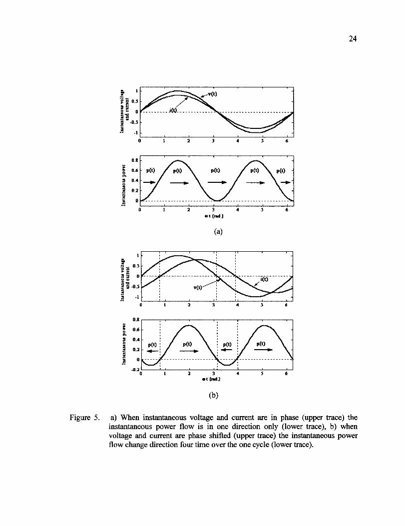
Reproduced with permission of the copyright owner. Further reproduction prohibited without permission.
24
0.1
; 0.6 0 Po ; 0.4 0
! O.l 1j
~ 0
0 2 3 4 5 6 ait [nd.]
(a)
~ ;l_ 0.5 oc:
; 5 0 0.,
l!-O..s .. • ~ -1
0 l 3 4 5 6
0.1 .. ; 0.6 0 Po
; 0
3 0.2 ;; • ~
2 3 4 5 6 ait (nd.]
(b)
Figure 5. a) When instantaneous voltage and current are in phase (upper trace) the instantaneous power flow is in one direction only (lower trace), b) when voltage and current are phase shifted (upper trace) the instantaneous power flow change direction four time over the one cycle (lower trace).

Reproduced with permission of the copyright owner. Further reproduction prohibited without permission.
25
The part of the surface that is bellow OJt axis is considered to be negative and is subtracted
from the part of the surface above OJt axis. It means that, for the same amplitude of the
voltage and current, the net power transferred from the source to the load is lower for the
phase shifted voltage and current. Because of the phase shift, for the constant voltage, to
provide the same average power, the current has to be increased. Increased current means
higher losses and higher inductive as well as resistive voltage drop.
The same principles apply to three phase circuit. The advantage of the three phase
balanced system over the one phase system is in the fact that instantaneous power is not
pulsating but constant physical entity.
2.4 Nature of Voltage Boost
Consider simple circuit shown in Fig.6. illustrating the bus voltage v(t) that is to be
regulated and a compensator, that is represented as a voltage source vc(t) behind
inductance L. The inductance L can be a transformer leakage reactance.
Figure 6 Voltage support of line voltage is provided with voltage source behind inductance L.
If the compensator voltage vc(t) is synchronized (in phase) with the bus voltage v(t) that is
to be regulated, the net (average) active power flow between two of them is zero. As two
voltages are in phase, the current ic(t) flowing between two of them is consequence of the

Reproduced with permission of the copyright owner. Further reproduction prohibited without permission.
26
voltage gradient only (difference in magnitude). If the both voltages are of the same
magnitude there is no current flow between them. The change in the magnitude of the
compensator voltage vc(t) change the current polarity. When the current polarity is
changed, the polarity of the voltage drop across the inductance L is changed too, as
shown in Fig.6, so the voltage drop across the inductance L can change from voltage
boost to voltage drop and vice versa, depending on polarity of the current ic(t):
diJt) v(t) = L----;}1 + vc(t) (2.20)
One may be tempted to think that voltage boost (drop) depends upon inductance value L.
The compensator current ic(t) can be calculated as:
(2.21)
as consequence:
(2.22)
as it can be seen from (2.22), the voltage boost does not depend upon L if the source of
compensating current ic is voltage source behind inductance because the current through
the inductance depends on inductance itself.
2.4.1 Phasor Approach
As the voltages and currents are sinusoïdal it is helpful to use phasor notation.
(2.23)

Reproduced with permission of the copyright owner. Further reproduction prohibited without permission.
27
(2.24)
(2.25)
or, using phasor notation
(2.26)
From (2.23) it can be seen that if V max >Vcmax the current ic(t) lagging after the voltages
Vc(t) and v(t) by 90° (inductive current) and if V max <V cmax the current ic(tJ is leading the
voltages vc(t) and v(t) by 90° (capacitive current). The two cases are represented by
Fig.7.a) and b).
v
v
(a) (b)
Figure 7 a) Vector diagram showing creation of voltage boost and b) voltage drop across inductance L.

Reproduced with permission of the copyright owner. Further reproduction prohibited without permission.
28
2.5 Voltage Drop Analysis
2.5.1 Equivalent Circuit
Every power system, regardless of its topology, seen from the point of coupling with
power delivery substation can be represented as Thévenin equivalent circuit as illustrated
in Fig.8. The Thévenin voltage V Th and impedance ZTh can be readily obtained from short
circuit current Ise, short circuit capacity Ssc and XIR ratio of the supply system as:
(2.27)
where ZTh=R+jX
These parameters are well known in engineering practice. The equivalent impedance ZTh
is usually inductive in meshed system, however it can be capacitive in case of long lines.
The Thévenin impedance ZTh can be considered as fictional, radial transmission line. The
Thévenin voltage V Th can be considered as sending end voltage V 5• V R and V L stand for
receiving end and load voltage respectively while XT is power delivery substation
reactance and IL load current.
V,~-~-f-f~T VL 1 ,_
tiL NETWORK
EQUIVALENT _
Figure 8 Power system seen from point of coupling with power delivery substation.

Reproduced with permission of the copyright owner. Further reproduction prohibited without permission.
29
2.5.2 Non-Compensated Line
In order to get better insight in voltage drop in the lines and action to remedy it, it is
useful to represent the line and the transformer as lumped inductance and consider simple,
one line transmission system with one bulk power delivery transformer and load as shown
in Fig.9 a). As it has been shown in the previous subsection it is very general case.
(a)
(c)
(b)
lp._u.
Figure 9 a) Single line diagram of radial transmission line GX). Line is connected to infinite bus with voltage Vs= lp.u. Transformer XT connects line to load, b) Current phasor c) complete phasor diagram. Voltage drop is caused by the load current IL across line reactance jX and supply transformer jXT.
To highlight the essentials, following is assumed:
1. The line is connected to infinite bus.

Reproduced with permission of the copyright owner. Further reproduction prohibited without permission.
30
2. The line is short and it can be represented by its series reactance jX.
First we consider the non compensated line from Fig. 9. The current IL drawn by the load
is inductive and can be decomposed into two components, one that is in phase IL<J, and
another inductive -jiLq in quadrature with load voltage VL (Fig.9.b). The load current
causes the voltage drop j(X+Xr)( kd-jiLq) in the transformer and line reactance,
decreasing receiving end voltage VR and load voltage VL, as shown in Fig.9.c).
2.5.3 Power Factor Correction
The power factor correction indicate that ali reactive requirements of the load are satisfied
locally. The power factor of the load is mostly corrected with switched/fixed capacitors
installed in parallel with load. After the power factor of the load is corrected locally by
injecting capacitive current +jkq, the inductive component of the load current -jiLq and
the voltage drop ~VL = (X+Xr)ILq it causes are cancelled, as shown in Fig.lO b). The
voltage drop caused by the ILd component of the load current still persists, preventing load
voltage from being 1 pu.
(a) (b)
Figure 10 a) The reactive requirement of the load are supplied locally. b) After power factor correction, voltage drop is partially mitigated.

Reproduced with permission of the copyright owner. Further reproduction prohibited without permission.
31
2.5.4 Voltage Regulation
The compensator is treated as reactive current source. To cancel voltage drop and to keep
load voltage V L at nominal value, the additional capacitive current has to be injected into
the system. The capacitive current can be injected on distribution or on transmission level
as illustrated in Fig. 11. If the voltage support is provided on distribution level (switch S2
on and SI off) the injected capacitive current is perpendicular to distribution voltage VL .
If voltage support provided on transmission level(switch S2 off and SI on) the injected
capacitive current is perpendicular to nodal transmission voltage Va. In both cases the
line current 1 is vector sum of load current and compensation current.
Figure 11 Single line diagram of radial transmission line GX). Line is connected to infinite bus with voltage Vs = 1p.u. Transformer XT connects line to load. Voltage support can be provided on transmission level (SI on, S2 off) or on distribution level (SI off, S1 on).
First we consider the non compensated line (Fig. 11 with switches SI and S2 off). The
power factor of the load is assumed to be corrected as shown previously. The current
drawn by the load depends on load itself and the voltage V L· The current causes the
voltage drop in the transformer and line reactance. It results in decrease in transmission
voltage V a and the load voltage V L· The load voltage V L is in phase with current drown
by the load. This is represented by the vector diagram as shown in Fig.12.

Reproduced with permission of the copyright owner. Further reproduction prohibited without permission.
32
\\Vs
Figure 12 Voltage drop caused by the load current IL across the line reactance jX and distribution transformer jXr
Linearity of the circuit in Fig.ll makes it possible to apply superposition theorem in order
to compare contributions of each compensator in voltage support. The circuit in Fig.ll
can be represented as a sum ofthree circuits shown in Fig. 13. a), b) and c).
(a) (b)
jX /lVI L
(c)
Figure 13 Circuit from Fig.ll decomposed according to the principle of superposition (a) without compensation, (b) voltage support provided on distribution side of power delivery substation, ( c) voltage support provided on transmission si de of power delivery substation

Reproduced with permission of the copyright owner. Further reproduction prohibited without permission.
33
From Fig.13. b) it is possible to evaluate value of the voltage support due to reactive
current injection led on the distribution si de of substation:
(2.28)
(2.29)
d V L d is voltage boost of the load voltage V L due to current led injected by the
compensator on the load side. The plus sign indicate that it is voltage drop, but due to the
fact that the voltage drop given by (2.28) is in opposite direction according to the voltage
drop caused by the load current IL in transformer and line reactance lj(X+XT) in Fig.ll, it
is actually the voltage boost.
Influence of injected compensating current led on distribution side of the substation on
transmission voltage is given by:
-d RjlcdjX RlcdX dVR = R+ j(x +Xr) =- R+ j(x +Xr)
(2.30)
Equation (2.30) give voltage boost on the transmission side of the substation. (Minus sign
depicts the fact that voltage drop is negative (negative voltage drop is boost), and the part
of the compensator current flowing through the line impedance jX has the same direction
as total current flowing through the line - the current 1 in Fig.ll.
If the compensation current is injected on transmission side of substation as shown in
Fig.13 c)

Reproduced with permission of the copyright owner. Further reproduction prohibited without permission.
34
(2.31)
(2.32)
- 1 (R + jXr )ilcdX Xlc1(R + jXr) ,1. VR = R + i( x + x T) = - R + i( x + x T) (2.33)
ifboth injected currents are equal in magnitude lied!= lied then from (2.29) and (2.30)
(2.34)
From (2.34) it can be seen that both placement of compensators provide voltage boost on
distribution side of the transformer XT, but the voltage boost is more pronounced when
compensator sat on distribution side due to transformer reactance XT.
The influence of two compensating schemes on transmission side voltage V T can be
compared from (2.30) and (2.33). Again, for same magnitude of the compensating
currents
(2.35)
From (2.35) it can be seen that in both cases transmission voltage VR is supported, but the
support of transmission voltage is more efficient in case of compensator on high voltage
side of the transformer XT.

Reproduced with permission of the copyright owner. Further reproduction prohibited without permission.
35
2.6 Conclusion
In this chapter the mechanisms of power transfer, voltage drop and voltage boost has been
discussed. lt has been shown that the nature of the inductive voltage drop and voltage
boost is in the phenomenology of electromagnetic field and Faraday-Lenz law. Moreover,
it has been shown that voltage drop across the inductance can be changed into voltage
boost if the polarity of the current through inductance is changed.
Finally, a simple power system consisting of the infinite bus, radial transmission line,
power delivery transformer and load has been analyzed using principle of superposition.
The influence of the voltage support provided on transmission and distribution level has
been analyzed. It has been shown that, when voltage support is provided on distribution
level the transmission voltage is supported too and vice versa.

Reproduced with permission of the copyright owner. Further reproduction prohibited without permission.
CHAPTER3
VOLTAGE SOURCE CONVERTER AS A STATCOM
3.1 Introduction
Benefits of reactive power compensation are well known: increased stability, increased
transmission capacity over existing lines, better voltage profile and decreased losses. As it
has been mentioned in chapter one, the management of reactive power by traditional
means has its drawbacks, depending on compensation technique used. These include a
possibility of resonance, slow response, introduction of harmonies, rotational instability
or management of reactive power in discrete steps. Moreover, if capacitor banks are used
(with or without thyristors), they occupy a considerable amount of real estate. The new
generation of static compensator based on converter circuits can successfully overcome
those problems and allow reactive power compensation without using bulky capacitors.
Unfortunately, the voltage rating of semiconductor switching deviees is not high enough
for high voltage application. To cope with this problem, a few switching deviees must be
put in series, or different multilevel topologies are to be used. Multilevel topologies have
their advantages over simply putting switching deviees in series. These include a better
output voltage waveform while FFM (fundamental frequency modulation) switching
strategy is used so that filters can be avoided and switching losses decreased. Voltage
stress dv/dt in the switching deviees is limited to one level of voltage so that converter
rating can be increased, allowing direct coupling with AC system without step up
transformer. However, the application of power electronic converters are suited to
distribution bus voltages and sizes. This is because they are based on solid-state
technologies, which have grown from the application of thyristors, gate-turn-off thyristors
(GTOs) and insulated gate bipolar transistors (IGBTs) to variable speed AC motor drives.
The controllers of SVS such as the Static V AR Compensators (SVCs) and the STATic
COMpensator (STATCOM), are solid-state switch technologies pushing upwards to the

Reproduced with permission of the copyright owner. Further reproduction prohibited without permission.
37
higher MV A ratings of power utilities. In fact, this has been one motivation of multi-level
converter research. Sorne manufacturers have already mastered the technology of
connecting GTOs or IGBTs in series to increase the voltage ratings of STATCOMs to
distribution voltage levels so that they can now be connected directly, without
transformers, to the electric utility[47,48].
In this chapter a review of STA TCOM princip les are presented. The original STATCOM
control strategies for voltage control of power system is tailored and tested. Numerical
simulation using Hypersim is used to validate proposed control strategy. The positioning
ofthe STATCOM in transmission line is discussed too.
3.2 Voltage Source Converter
STATCOM is basically AC voltage source behind the reactance as illustrated in Fig.6.
Voltage source converter (VSC) is used as a voltage source. Fig. 14 a) illustrates one
converter leg of basic three phase converter circuit and Fig.14 b) illustrates three phase
six pulse converter topology. The VSC is an array of power electronic switching deviees,
that, with their fast switching action, can shape DC voltage to AC and AC to DC. While
doing it, the phase and magnitude of AC voltage can be controlled, so as the power flow
through the converter. While doing conversion, the harmonies are introduced into the
power system also. The output square waveform is shown in Fig. 14 a). It consist of
fundamental component and spectra of odd harmonies. In three phase configuration, due
to 120° phase shift between three output AC voltages third harmonie and its multiple will
get canceled for balanced circuit in line to line voltage.
The advantage of the ST A TCOM over traditional synchronous compensator is lack of
inertia providing fast response without introduction of oscillation and lack of rotational
parts lowering maintenance requirements. The disadvantage is introduction of harmonies,
rating of switching devises and switching losses and high initial cost. To decrease

Reproduced with permission of the copyright owner. Further reproduction prohibited without permission.
38
harmonie content in the output voltage waveform, PWM or sorne other fast switching
strategies has to be used but that may lead to increase in switching losses. Moreover,
power switching deviees has limited voltage and current ratings, so the switches have to
be put in series and in parallel which may lead to gating problems.
(a) (b)
Figure 14 Basic six pulse converter circuit. a) one converter leg with its output AC voltage waveform, b) three phase circuit.
To decrease switching losses, increase rating and improve output voltage waveform, the
six pulses converters are combined as shown in Fig.15, cascaded or multilevel topologies
are used for power system applications .
..... ·a ~
v, u vb .~
Q) v, = Y.ox 01)
tl:! 2 ~
Figure 15 Inverter coupling with magnetic circuit

Reproduced with permission of the copyright owner. Further reproduction prohibited without permission.
39
3.3 Diode Clamped VSC
One of the most popular multilevel converter topologies for high voltage application is so
called "diode clamped" topology. Fig.16 shows one phase of five-level diode clamped
VSI together with its output voltage waveform. The topology that was proposed by Nabae
et al. [30] had initially only three levels controlled by PWM modulation strategy. The
three-level diode clamped VSI gained a lot of attention for high voltage applications and,
very soon, has been upgraded with the new levels [31] and enhanced [32]. Because of its
advantages such as decreased THD, off-line optimization of switching angles, increased
voltage rating and diminished dv/dt stress, the topology has been suggested for different
high voltage applications such as STATCOM, UPFC and back to back DC link [35-38].
However, there are sorne important drawbacks such as complicated construction, unequal
current stress on switching deviees and capacitor voltage balancing problem. The
capacitor voltage unbalance depends upon switching angles and net active power
transferred between AC and DC si de of inverter. If this transfer is zero, than the problem
disappears. Because of the capacitor balancing problem, the most sui table application for
diode clamped multilevel VSI is ST ATCOM. In the case of ideal STA TCOM, the net
active power exchange between AC and DC side of inverter circuit is zero during steady
state operation. The capacitor balancing problem has been solved in [60].
3.3.1 Topology description
Fig.16 shows one phase offive-level diode clamped inverter. The DC bus ofthe N level
inverter consists of N-1 capacitors that allow N taps for N levels of voltage. The
capacitors are common for all three phases. One phase of power circuit has (N-1)x2
power switches and (N-2)x2 clamping diodes. Each switching deviees has to stand one
voltage level.
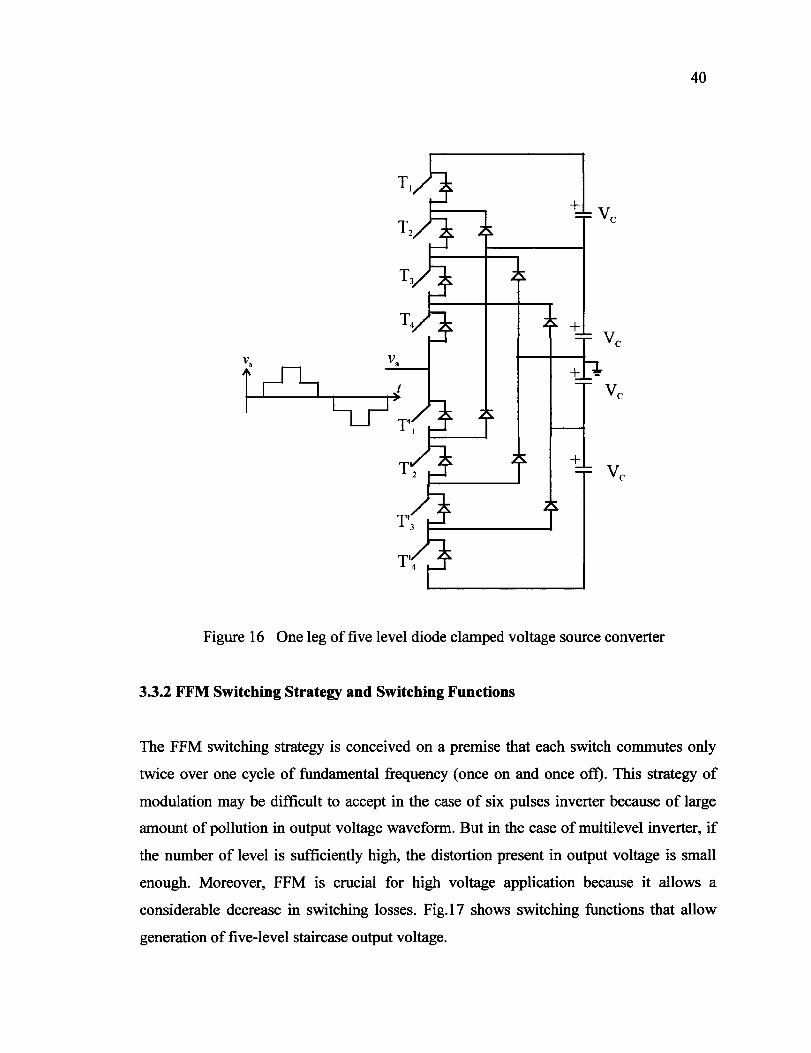
Reproduced with permission of the copyright owner. Further reproduction prohibited without permission.
40
+
+
Figure 16 One leg of five level diode clamped voltage source converter
3.3.2 FFM Switching Strategy and Switching Fonctions
The FFM switching strategy is conceived on a premise that each switch commutes only
twice over one cycle of fundamental frequency (once on and once oft). This strategy of
modulation may be difficult to accept in the case of six pulses inverter because of large
amount of pollution in output voltage waveform. But in the case of multilevel inverter, if
the number of level is sufficiently high, the distortion present in output voltage is small
enough. Moreover, FFM is crucial for high voltage application because it allows a
considerable decrease in switching losses. Fig.17 shows switching functions that allow
generation of five-level staircase output voltage.

Reproduced with permission of the copyright owner. Further reproduction prohibited without permission.
41
Switching deviees T 1, T 2, T 3 and T 4 have for their complements T 1 ', T 2', T 3' and T 4'. If
T 1 is forced to close, T 1' is forced to open and vice versa. The same is true for the other
deviees. The voltage on the DC side of the converter V oc consists of four equal voltages
V c, where V c is voltage across one of the four capacitors that form DC bus. The
switching deviees are controlled by switching function given by Fig 17. The shaded areas
show that transistors are in conduction. Output voltage waveform consists of five-level
2Vc, Vc, 0, -Vc and -2Vc.
to obtain voltage level 2V c, transistors T 1, T 2, T 3 and T 4 are closed and their
complements Tt', T2', T3' and T4' are open.
to commute to voltage level V c, transistor T 1 is forced to open an T 1' to close
to commute to voltage level 0, T 2 is forced to open an T 2' to close.
to commute to voltage level -V c, T 3 is forced to open and T 3' to close
to commute to voltage level-2Vc, T4 is forced to open and T4' to close.
o, ~1 ~ 'IUl 11:$ 11:~1 11:11:% 11:$ 3'lCI2 211:-(X, 21[..(1.~ 1 1 t 1 1 1
' 1 1 1
T,
T,
Figure 17 Switching function for five-level voltage source converter
By returning in reverse direction the full cycle is described. Repeating given pattern, the
staircase quasi-sinusoïdal voltage output waveform is obtained. The voltage stress on
transistors dv/dt is limited to one level that is voltage V c across one of the capacitor on
the DC side of converter. The current path through converter depends on the voltage level
and sign of the current. The current stress is not equally distributed among switching

Reproduced with permission of the copyright owner. Further reproduction prohibited without permission.
42
deviees and that it is more pronounced for inner switching deviees (T4 and T1 ') than for
outer switching deviees (TI and T4'). As a consequence, the rate of charging and
discharging inner capacitors C2 and C3 is higher than that of outer capacitors C1 and C4,
so that the voltage across the inner capacitors will tend to increase or decrease more than
the voltage across outer capacitors, depending on the mode of operation ( capacitive or
inductive). The voltages across capacitors must be balanced in order to prevent distortion
of the output voltage and to ensure the even voltage stress dv/dt in the switching deviees.
Equalizing DC capacitors voltages can be achieved by additional hardware [31] or within
control algorithm [38],[60]. The voltage balance problem does not exist in case of ideal
reactive operation ( converter currant lead or lag converter voltage by 90 degrees).
3.3.3 Voltage Output Waveform: Optimization
In general, one N-level diode clamped VSI can produce N-level output voltage waveform
(Fig.l8) and the line-to-line voltage can consist of 2N-1 levels. If the FFM switching
strategy is applied, then each switching deviee commutes twice per cycle, diminishing
switching losses.
N-level output voltage waveform produced using FFM switching strategy (Fig.18) is
symmetric and can be represented by series of Fourier:
00
4V: [ ] v(t) = ~ ,J: cosk~ +cosk~+ ... +coskaN-I sinkax k-I 2
(3.1)
k = 2n+1, n eN

Reproduced with permission of the copyright owner. Further reproduction prohibited without permission.
43
....................... Y~
v .............. !.....-----~
0 a(N-1)/2 switching angle
Figure 18 N-level output voltage waveform
From Fig. 18 it ean be seen that for N-level output voltage waveform (N-1)/2 switehing
angles a.1, a.2 to <X.(N-1)12 ean be ehosen in order to eliminate (N-1)/2 dominant harmonies
orto minimize (total harmonie distortion) THD. In other words, N-level eonverter has (N-
1)/2 degrees ofliberty. The amplitude ofkth harmonie is given by (3.2).
(3.2)
In the five-level output voltage waveform, two dominant harmonies ean be eliminated (5th
and 7th) by solving a set of equations given by (3.3), where Ai are Fourier coefficients
given by (3.2) for i=5,7.
(3.3)

Reproduced with permission of the copyright owner. Further reproduction prohibited without permission.
44
After finding solutions from (3.3), THD of phase voltage is 21.7%. The third harmonie
and its multiples are eliminated in the line-to-line voltage. The line-to-line voltage is
given by (3.4) and THD ofline-to-line voltage is 8.56%.
(3.4)
The other solution, appropriate for one phase converter, is to minimize THD. The
function of THD for the five-level inverter is given by (3.5) where f(a., a2) is given by
(3.6).
(3.5)
(3.6)
After minimizing the function f(at, a2), THD of the phase voltage is 16% and THD of
line voltage is 1 0.8%. In both case the line voltage consists of nine levels. The RMS value
of phase N-level output voltage is given by (3.7) and RMS of fundamental is given by
(3.8).
2 2Vc N- tr 2 [( 1) 2
] V RMS =-;;- -2- 2- a1 - 3a2 - 5a3 -7a4 + ... +(N- 2)aN
2
_ 1 (3.7)
2 8Vc 2 [ ]2 v;RMs = 7 cosa1 + cosa2 + ... +cosaN;t (3.8)

Reproduced with permission of the copyright owner. Further reproduction prohibited without permission.
45
It is worth noting that magnitude of the inverter output voltage, if the off-line
optimization applied, depends exclusively on the value of the voltage V c across the
capacitor on the DC side of inverter. If the off-line optimization is not applied, then this
magnitude can be controlled by changing switching angles ai .More details an be found in
[ 61]. Sorne other modulation strategies such as pulse width modulation (PWM) or
selective harmonies elimination (SHEM), which result with even better output voltage
waveform, can be used, but they impose higher speed of switching, which may not be
acceptable in high voltage applications.
3.4 VSC Equivalent Circuit
Fig.19 illustrates three phase Voltage Source Converter equivalent circuit. The AC side of
the converter is modeled by voltage sources Va, V1J and Vc while DC si de of the converter is
modeled as current source loc and capacitance [46]. The DC current loc is converter DC
current. To model the switching and capacitive losses the resistance can be added in DC
side of the converter. The AC and DC side of the converter are related through power
balance equation:
(3.9)
t
Figure 19 VSC equivalent circuit

Reproduced with permission of the copyright owner. Further reproduction prohibited without permission.
46
3.5 Proposed Control Strategy for ST ATCOM
Fig.20 shows block diagram of the STATCOM control circuit. The primary objective of
the control system is to provide the adequate voltage support. This is achieved by
controlling the amplitude of STATCOM output voltage as described in section 2.6. When
voltage support is needed, the STATCOM output voltage is increased, and STATCOM
provides reactive power. During period of light loading of transmission line, when
voltage has tendency to arise, the STATCOM output voltage decreases, ST ATCOM
absorbs reactive power (or supply less reactive power), and controls the line voltages as
illustrated on vector diagrams in Fig. 7 a) and b ). A detailed description of control
strategy is given in [62,63]. In this work the control strategy is conceived on low
frequency PWM modulation. The DC voltage on DC bus of the power converter is kept
constant. The relation between amplitude of STATCOM output voltage VsrAr., and the
voltage on the DC bus V oc is given by:
(3.10)
where rn is modulation index. In order to control V STAr., the modulation index rn is varied
and DC bus voltage is kept constant. The outer control loop allows active power control.
The PLL (phase lock loop) allows synchronization of the STATCOM output voltage with
the AC system. lts robustness is crucial for the performance of the ST ATCOM. The PLL
must be able to lock up the phase of line voltage immediately after disturbances. lts
output is phase angle. DC bus voltage of the ST ATCOM is measured, filtered and
compared to the reference value. The error is processed through Proportional-Integral (Pl)
block. The output of PI block is used as phase shift reference 8 that is added to PLL
output. The sum of the two signais gives phase angle reference for the STATCOM output
voltage allowing the flow of active power from line into the ST ATCOM in order to meet
its }osses. The inner control loop has faster dynamic and allows reactive power control.

Reproduced with permission of the copyright owner. Further reproduction prohibited without permission.
47
The instantaneous values of the three phase voltages Va, Vb and v c on the supported bus are
measured and RMS value ofmidpoint voltage VRMs· is computed using
(3.11)
The computed value is compared with v* RMS the desired value of the line voltage. The
error signal is processed in PI block and applied as modulation index. The distinct
advantages of this type of control are following:
1. There is no need to measure current, therefore, getting rid of the current transformers.
2. The active and reactive power control are completely decoupled.
Phase LockedLoop
(PLL) Voltage
Measurement
Figure 20 STATCOM control circuit

Reproduced with permission of the copyright owner. Further reproduction prohibited without permission.
3.5.1 Phased lock loop (PLL)
Fig. 21 shows the structure of PLL. The PLL is designed for three phase operation.
abc to a.j3 Phase Transformation i Detector
LowPass Fil ter
Fil ter
1 s
Voltage Controlled Oscillator
Figure 21 Phased lock loop-block diagram
e
48
The instantaneous line voltages Va, Vb and Vc are measured and transformed in a.-J3
reference frame. The PLL consist of three parts: phase detector, filter and voltage
controlled oscillator. The line voltages are given by:
va =v maxsin(mt + ço) 21l
vb =V maxsin(ax + ço-3) 2;r
vc = v maxsin(ax + ço + 3)
After the transformation in in a.-J3 reference (3.12) becomes (3.13).
(3.12)

Reproduced with permission of the copyright owner. Further reproduction prohibited without permission.
v a = v max sin( W( + qJ)
Vp = Vmax. COS(wt + qJ)
49
(3.13)
The phase angle of the line voltage is rot+cp. The output of the phase detector is given by
(3.14):
Ua = VaUva- VpUvp =V maxKL[sin(ax + qJ)cos{}- CO~ax + qJ)sinO] = V maxKL sin( mt + qJ- B)
Angle e can be written as {)=mt+ IPJ. therefore (3.14) becomes:
Assuming that PLL is locked, (3.15) can be linearized and rewritten as:
(3.14)
(3.15)
(3.16)
Signal obtained from (3.15) is passed through low pass filter that is PI block whose
proportional and integral gains are Kp and Kr respectively so the output of the fil ter is:
11m = Kvu 1
m = % + 11m
where ro is PLL frequency and finally phase angle is:
t
(} = m0t + J !1axlt -a:J
(3.17)
(3.18)

Reproduced with permission of the copyright owner. Further reproduction prohibited without permission.
50
3.5.2 Positioning of STATCOM
The optimal positioning of voltage support deviees in transmission line has been
investigated in [9,63],[65-67]. It has been stated in [9,65] that, when dynamic voltage
support deviees positioned in mid point of the transmission line power transfer can be
doubled. The voltage profile of the line is given with solution of the wave equation:
Assuming lossless line the solution is given by:
V = VR cos fJx + jZJ R sin fJx
Zc is characteristic impedance of the line
p = m.Jk is wave number
1-line inductance (Hikm)
c-line capacitance (F/km)
(3.19)
(3.20)
If the active and reactive power of the load are P+jQ, the sending end voltage(source
voltage) is (3.21):
V R receiving end voltage
Vs sending end voltage
9=~1, 1 line length (km),
9 - electricalline length
(3.21)
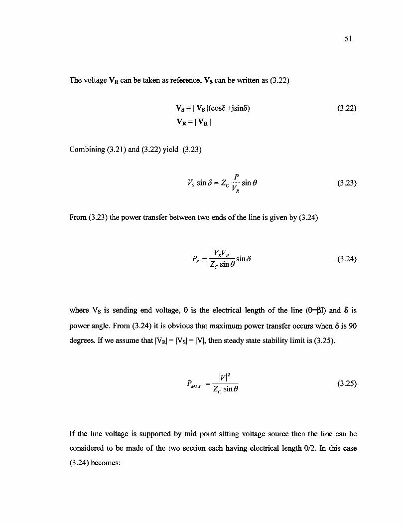
Reproduced with permission of the copyright owner. Further reproduction prohibited without permission.
The voltage Vacan be taken as reference, Vs can be written as (3.22)
Vs= 1 Vs l(cos<> +jsinô)
Va=IVal
Combining (3.21) and (3.22) yield (3.23)
From (3.23) the power transfer between two ends of the line is given by (3.24)
51
(3.22)
(3.23)
(3.24)
where Vs is sending end voltage, e is the electrical length of the line (9=J3l) and o is
power angle. From (3.24) it is obvious that maximum power transfer occurs when ois 90
degrees. If we assume that IV RI = IV si = lVI, then steady state stability limit is (3 .25).
IVI2
p = ---'----'---MAX. Zc sine
(3.25)
If the line voltage is supported by mid point sitting voltage source then the line can be
considered to be made of the two section each having electrical length 9/2. In this case
(3.24) becomes:

Reproduced with permission of the copyright owner. Further reproduction prohibited without permission.
52
(3.26)
where 1 V M 1 = lVI is mid-point voltage.
In this case the steady state stability limit is given by (3.27)
IVI 2
p MAX .COMP = (} Z sin-
e 2
(3.27)
The increment in steady state maximum power transfer depends upon the line length and
is expressed as (3.28):
sin(} p MAX.COMP = p MAX. -----:-a
sm-2
(3.28)
where PMAX.COMP. is maximum steady state transferable power of mid-point compensated
line and PMAX. is maximum steady state transferable power of the non-compensated same
line. In case of short line sine~ e and sin(9/2) ~ 9/2 and (3.28) becomes (3.29)
(3.29)
In the reality, the maximum power that can be transferred over the transmission line is
limited by transient stability of the power system. The transient stability limit can be
determined by using equal-area stability criterion. The stable operation of mid point
compensa~~d li~ with controllable voltage source is extended in the second quadrant
(90° <ô<180°).
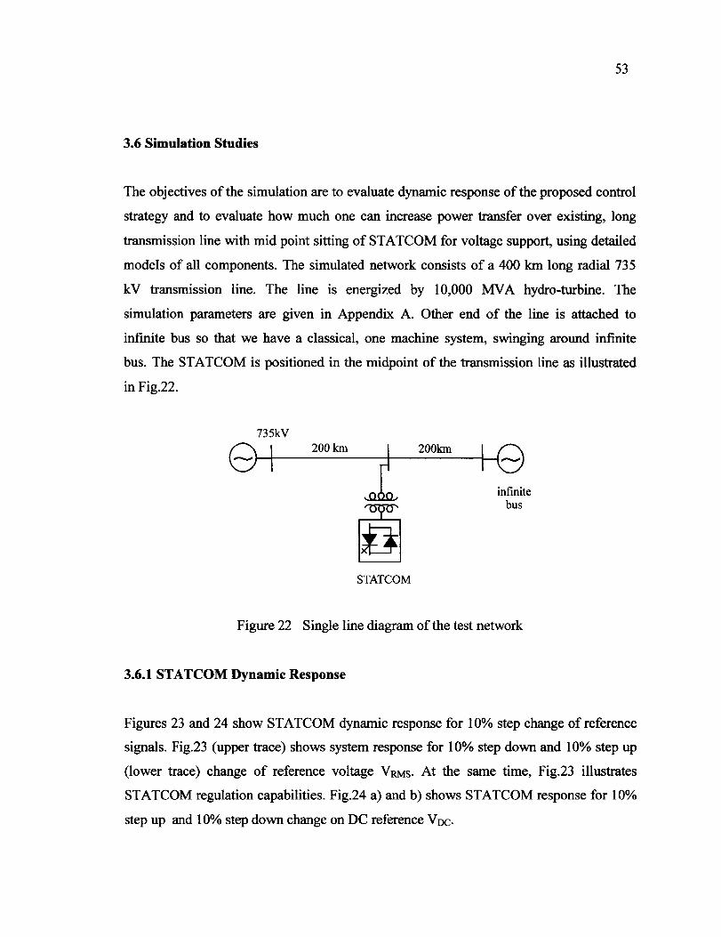
Reproduced with permission of the copyright owner. Further reproduction prohibited without permission.
53
3.6 Simulation Studies
The objectives of the simulation are to evaluate dynamic response of the proposed control
strategy and to evaluate how much one can increase power transfer over existing, long
transmission line with mid point sitting of STATCOM for voltage support, using detailed
models of ali components. The simulated network consists of a 400 km long radial 735
kV transmission line. The line is energized by 10,000 MV A hydro-turbine. The
simulation parameters are given in Appendix A. Other end of the line is attached to
infinite bus so that we have a classical, one machine system, swinging around infinite
bus. The ST ATCOM is positioned in the midpoint of the transmission line as illustrated
in Fig.22.
735kV
8~\ _2o_o km -rt+---2ookm____,k9
~ infinite
~ bu"
STATCOM
Figure 22 Single line diagram of the test network
3.6.1 STATCOM Dynamic Response
Figures 23 and 24 show STATCOM dynamic response for 10% step change of reference
signais. Fig.23 (upper trace) shows system response for 10% step down and 10% step up
(lower trace) change of reference voltage VRMs- At the same time, Fig.23 illustrates
STATCOM regulation capabilities. Fig.24 a) and b) shows STATCOM response for 10%
step up and 10% step down change on DC reference V oc.

Reproduced with permission of the copyright owner. Further reproduction prohibited without permission.
.. ~0.95 ..
llO • .!! > 0.9
... ~0.95
.., œ
0
~ ô 0.9~---'
> 0
0.5
0.5 Time [sec.]
54
Figure 23 STATCOM dynamic response for 10% step down change in reference voltage and 10% step up change in reference voltage
tl : : ~ j }":t : : t l 0 05 1 15 l 0 05 1 15 l
; J : -J-l ;.~t : -~[_] 0 O.l 1 l.l l 0 0..5 1 l.l 2
r ..... (sec.) r .... [sec.)
(a) (b)
Figure 24 a) STATCOM dynamic response for 10% step up change in DC reference. Upper trace shows measured AC line voltage and lower trace shows DC bus voltage. b) STATCOM dynamic response for 10 % step down change in DC reference.

Reproduced with permission of the copyright owner. Further reproduction prohibited without permission.
55
3.6.2 Steady State Stability
In order to investigate the power transfer steady state and transient stability limits, the
system described above is simulated without and with STATCOM. For the analysis of
steady-state performance, the power supplied by the generator-turbine unit is increased
gradually. After each power increment, the simulated system is allowed to regain the
stable point of operation. The power transferred over the line is measured. The maximum
power that can be stahly transferred without mid-point sitting STATCOM for voltage
support is 4300 MW. When the STATCOM installed, the maximum power increases to
7450 MW. One can see that power transfer is increased during the steady-state by the
factor of 1. 732. The power transfer is not increased by the factor of two as expected in
[ 65]. The reason is while power is increased, the line and transformer losses increase
because of higher current. The second reason is that the line voltage is already naturally
supported by line distributed shunt capacitance as shown in (3.28).
3.6.3 Transient Stability
The same system is subjected to transient stability test. The power loading is increased
gradually and system is allowed to stabilize. Then three phase short circuit is applied in
the vicinity of the generator unit (30 km from generator) and is cleared after 100 ms. The
system must reestablish to the same power transfer level as before the short circuit in
order to remain stable. The maximum power that can be transferred stahly is 4000 MW
without the STATCOM and 6400 MW with STATCOM sat in the middle of the line,
which is an increase by a factor of 1.6.
3. 7 Conclusion
The STATCOM based on power converter has been discussed in this chapter. An original
control strategy for voltage support of transmission lines by STATCOM has been

Reproduced with permission of the copyright owner. Further reproduction prohibited without permission.
56
presented and evaluated using a test system. The results of case analysis obtained by
detailed numerical simulation have shown that ST ATCOM can significantly increase
steady state and transient stability limits and hence transmission capacity of existing lines,
while providing voltage support. When STATCOM put in the middle ofthe 400 km, 735
kV line, it is known to be optimal placing for the radialline, the steady state stability limit
is increased by 73% and transient stability limit is increased by 60%. The power transfer
can not be doubled due to the line length, losses and transformer and generator
impedances. At the same time, voltage of the line is kept constant, independently of the
loading which contributes significantly to power quality. It makes STATCOM attractive
and cost effective alternative to building new line.

Reproduced with permission of the copyright owner. Further reproduction prohibited without permission.
CHAPTER4
VOLTAGE SUPPORT BY DISTRIBUTED STATIC V AR SYSTEMS (SVS)
4.1 Introduction
In this chapter it is shown that when load centers require Static V AR Systems (SVS) for
regulated voltage control, the strategy of using many, small, distributed SVS located at
distribution buses is more advantageous than a few large bulk SVS located at the
transmission or sub-transmission bus. The advantages are: (i) standby to meet N-1
reliability criterion is reduced; (ii) costly high voltage transformers are no longer needed
because the SVS can be connected directly to the low voltage distribution buses; (iii)
distribution-side voltage support is more effective because the total MV Ar requirement of
the distributed SVS is less. Simulation studies have demonstrated that the distributed SVS
units operate harmoniously together.
Faced with the difficulty of securing rights-of-way for new transmission lines, increasing
reliance is placed on Static V AR Systems (SVS) to provide voltage support to the
increasingly overloaded existing lines. In this chapter the term SVS is treated as a
continuously controllable source of reactive current. It represents a combination of
switched capacitors, switched inductance (for economy) and thyristor SVCs or
STATCOMs (to give continuously adjustable control between the capacitor steps).
Presently, large bulk SVSs are located at the transmission or sub-transmission buses. This
raises the specter of voltage collapse should the SVS fail. N-1 reliability criterion
requires a redundant set of SVS. This chapter presents a preliminary evaluation of the
alternative of using many small SVSs located at the low voltage distribution buses. With
distributed SVSs, when any one of theM units fails, there are still M-1 units remaining to

Reproduced with permission of the copyright owner. Further reproduction prohibited without permission.
58
provide voltage support. Apart from satisfying the reliability criterion better, distributed
SVS bring other savings as weiL
Historically, synchronous condensers, connected at the sub-transmission and transmission
buses, have been used to supply the continuously adjustable capacitive or inductive
currents to support the voltages at the load centers. Because of the precedence set by
synchronous condensers, the SVS which have largely supplanted them, still tend to be
situated at the sub-transmission and transmission buses. With the availability of
STATCOMs or SVCs (cheaper) which can be connected at distribution level voltages
without the need of transformers [47,48,68], it is timely to examine whether regulated
voltage support should be by:
or
(1) a single or a few bulk SVSs connected at the transmission or sub-transmission
buses.
(2) many small-sized distributed SVSs units connected at distribution buses.
This chapter presents the reasoning and sorne preliminary quantitative evaluations which
support the case for distributed SVS. The objective is to arrive at positive interim
conclusions which justify further in-depth studies further. The conceptual design of a
substation serving a load center is given at the end of the chapter. Lastly, simulations have
been used to show that many SVS units do not interact adversely to cause instability.
4.2 Model of Transmission Line to Load Center
A number of assumptions befitting a preliminary study have been used. Per-unit base
referred to the transmission voltage side is used in the study and resistive losses are
neglected.

Reproduced with permission of the copyright owner. Further reproduction prohibited without permission.
59
In order to highlight the mechanism of "voltage drop" and conversely "voltage support",
the radial transmission line is represented by an inductive reactance jX between the
sending-end voltage Vs and receiving-end voltage VR as illustrated in Fig. 25. The
''telegraph line equations" could have been used, but the purpose of this chapter is to
highlight the "mechanism" of voltage support using simple phasor diagrams. In presenting
a Conceptual Design in Section 4.8, the ''telegraph line equations" will be used to predict
the inductive and the capacitive MV Ars required to prevent overvoltage and undervoltage
when loading below and above the Surge Impedance Level (SIL), respectively. For the
present, the formula of the transmission reactance for different line length is X=0.0013 1
p.u. of the surge impedance, where 1 is the length in km. M equal loads taking load
currents IVM each is supplied from the bus of VR. Transformers, whose leakage
reactances are jMXT, bridge the high transmission line voltage VR to low the distribution
voltage VL of the loads. The transformer reactance is assumed to be Xr=O.lO p.u. The
distributed SVS supply current le~ directly at the load buses without transformers
because the distribution voltage is within the capability of existing SVS technology.
Figure 25
~ ÏJM
Single line diagram of transmission line (jX) between Vs and V R· M transformers (jMXT) connect transmission line to M loads. Distribution SVS currents Icd/M provide voltage support of load voltage V L·

Reproduced with permission of the copyright owner. Further reproduction prohibited without permission.
60
The M transformers and the loads of Fig. 25 have been replaced by single transformer of
reactance jXT and a single load current IL in Fig. 26. Fig. 26 a) and b), respectively, show
the bulk SVS compensation current lcb at the transmission voltage bus side and the
distributed SVS compensation current led at the distribution voltage bus side. Fig. 26 a)
includes an additional transformer which is required to raise the voltage output of the SVS
to the transmission line voltage ofVa.
---+ - HV l _
1Y transformer
lcb+~
(a)
Ys jX VR jXT VL
kxwl (~\ ~<i Qp, ---. led
I Icd+IL
(b)
Figure 26 Single line diagram with M loads of Fig.l equivalenced as a single load carrying current IL. (a) Bulk SVS connected to bus of Va by additional transformer; (b) Distributed SVS located at bus of V L·
4.3 Case For Distributed SVS
The findings of this preliminary study point to potential cost savings arising from: (i)
reduction of standby MV Ar needed to satis:fY N-1 reliability criterion; (ii) reduced MV Ar

Reproduced with permission of the copyright owner. Further reproduction prohibited without permission.
61
rating in the distributed SVS of Fig. 26 b ); (iii) not needing the high voltage transformer
ofFig.26 a).
4.3.1 Reliability
The loss of the bulk SVS in Fig. 26 a) affects the entire load center. N-1 reliability
criterion requires there must be K units, K=2,3,4, .. , on standby and each unit has to be
rated at the 1/(K-1) times the full MV Ar required. The total cost is expressed as K/(K-1)
times the full MV Ar required.
In the system of Fig. 26 b ), there are already M sets of distributed SVSs. It is a matter of
rating each SVS at 1/(M-1) times the full MV Ar required.
4.3.2 Effectiveness of Compensation
The "mechanism" of voltage control is complex and the details are outlined in the
analysis in Section 4.4. However the basic idea is simple: as viewed from the load, an
inductive current 1= -jli flowing across transmission line inductive reactance jX produces
a voltage drop of -Xli and a capacitive current 1= jlc produces a voltage boost of+ XIe. In
Fig. 26 a), the bulk SVS current Icb passes through the transmission line reactance jX
only. In Fig. 26 b) the capacitive current led passes through a larger reactance j(X+XT)
since the load transformer reactance jXT is added in the capacitive current path. Because
of the larger reactance j(X+XT), the compensation produces a higher voltage boost/drop in
Fig.26 b) than in Fig. 26 a). This simple-minded picture has been used as a guide only.
Rigorous circuit theory analysis in Section 4.4 is applied to compare the MV Ar
requirements ofFig. 26 a) and Fig.26 b).

Reproduced with permission of the copyright owner. Further reproduction prohibited without permission.
62
4.3.3 Potential Cost Saving of High Voltage Transformer
The bulk SVS in Fig. 26 a) requires a transformer to raise its output to transmission
voltages. Additional transformers are not required in Fig.26 b) because the distributed
SVS can be connected directly, without transformers, to the low voltage distribution
buses. Therefore, there is a potential saving in cost.
4.4 Voltage Regulation Analysis
Voltage support analysis has mostly been approached at the quadratic level of complex
power S=P+jQ. As will be shown below, the linear circuit theory approach using
complex phasors of voltages and currents is more insightful.
The base line used in the comparative studies is that the load is a unity power factor load,
i.e the load current k is in phase with the voltage of the load bus V L· As is weil known,
lagging power factor load depresses the load bus voltage further. The V ARs required to
correct the poor power factor will be accounted separately from the V ARs required for
voltage support of unity power factor loads. This is in line with the approach taken in the
classic reference. Following this approach, the objective is to derive the formulae of the
MV Ar required for voltage support exclusively.
4.4.1 Bulk V Ar Compensation at High Voltage Bus of V R
The phasor diagram of Fig. 27 is for the study of voltage regulation by bulk SVS located
at the bus ofVR in Fig. 26 a). When the bulk SVS regulates the receiving-end voltage VR
at 1.0 p.u. voltage, VL the magnitude of the load voltage VL must be less than 1.0 p.u.
(The per unitization is based on the voltage-base of the transmission line side.) The
voltage drop is due to the voltage across the transformer reactance jXT.

Reproduced with permission of the copyright owner. Further reproduction prohibited without permission.
63
lp.u.
: .·
Figure 27 Phasor diagram--system of Fig. 26 a), Bulk SVS at Transmission Bus.
4.4.1.1.Phasor Diagram of Load Transformer
Fig. 27 shows VL and k in phase for unity power factor operation, i.e. P=VL k. lt is
necessary to compute the load voltage magnitude VL for any load power P. For 1 VRI =1.0,
applying Pythagoras Theorem to the right angle triangle formed by VR, VL andjXTk
(4.1)
Substituting k=PNL, (4.1) yields a quadratic equation of( VL)2• Solving the equation and
choosing the solution which is nearest to 1.0 gives,
(4.2)

Reproduced with permission of the copyright owner. Further reproduction prohibited without permission.
64
The value of VL+ is defined as the solution of (4.2) for P=l.O. VL+ will be kept for the
analysis of distributed SVS below. Although V L + is less than 1.0 p.u., by choosing the
transformer turns ratio, the distribution bus voltage can be 35 kV or 25 kV of the
standard. The angle opposite to jX TIL is y. From the properties of right angle triangle,
y = arcco~Vt) (4.3)
4.4.1.2 Phasor Diagram of Transmission Line
In the triangle formed by Vs and V R enclosing the angle 28b, the power equation is
P _IFsll~l . 2(}. - sm b x (4.4)
1 ~ = 2arcsin(PX) (4.5)
The transmission line current 1 is perpendicular to jXI and bisects the angle 28b. The
current of the bulk SVS is: - - -Icb = 1- IL (4.6)
Icb lies along the constant power line so that
(4.7)
Icb consists of two parts: Icb vs for transmission line compensation (voltage support) and
IcbPF for transformer compensation (power factor correction). The SVS current
decomposed into the two components is

Reproduced with permission of the copyright owner. Further reproduction prohibited without permission.
65
(4.8)
Dividing (4.8) either the LHS or RHS of(4.7) and multiplying throughout by P, it can be
shown that the reactive power of the bulk SVS is
(4.9)
In (4.9), P tan eb is for compensating the reactance jX of the transmission line and P tan y
is for the reactance jXT of the transformers.
4.4.1.3 MV A Requirements of Transformers
In addition to the M load transformers, the bulk SVS requires a transformer to step up its
low voltage to high transmission line voltage.
4.4.1.3.1 MV A Ra ting Requirement of Load Transformers
The high voltage side of the load transformers must be rated at f VRI =1.0 p.u. The current
requirement is k=INL+· The MVA requirement of ali theM load transformers is 1 Sb
Loadl = INL+, for vL+ taken from (4.2) for the case P=l.O.
4.4.1.3.2 MV A Ra ting Requirement of Transmission Bus SVS Transformer
The MV A rating of the high voltage transformer must be 1 SbSvsl =P (tan8z+tany) for y
given by (4.3) and eb given by (4.5).

Reproduced with permission of the copyright owner. Further reproduction prohibited without permission.
66
4.4.2 Distributed V AR Compensation at bus of V L
Fig. 28 is the phasor diagram of Distributed SVS compensation. In order that the
comparison is on the same foot, the load voltage is regulated at 1 V L 1 =1 V L +1 and the load
power Pis delivered at unity power factor. The closing side of the voltage triangle formed
by Vs and vL+ is j(X+XT)I. 1 lies perpendicular to j(X+XT)I and makes an angle ed with
vL+· The angle Blies between and Vs and vL+·
The real power P is
(4.10)
ForVs=l,
(4.11)
The angle, which 1 makes with V L' is ed. The angle, which 1 makes with Vs, is (8-9d). The
power transmitted at Vs is P=1 1 1 cos (8-9d). The power received at V L + is P=1 V L -H 1 1
1 cosed. Equating the two powers,
(4.12)
Substituting the trigonometry identity cos(8-9d)=cos8 cosed + sin8 sin ed in (4.12), it can
be shown that
~~+1- cosg Ba = arctan . s:
smu (4.13)
The current of the distributed SVS is
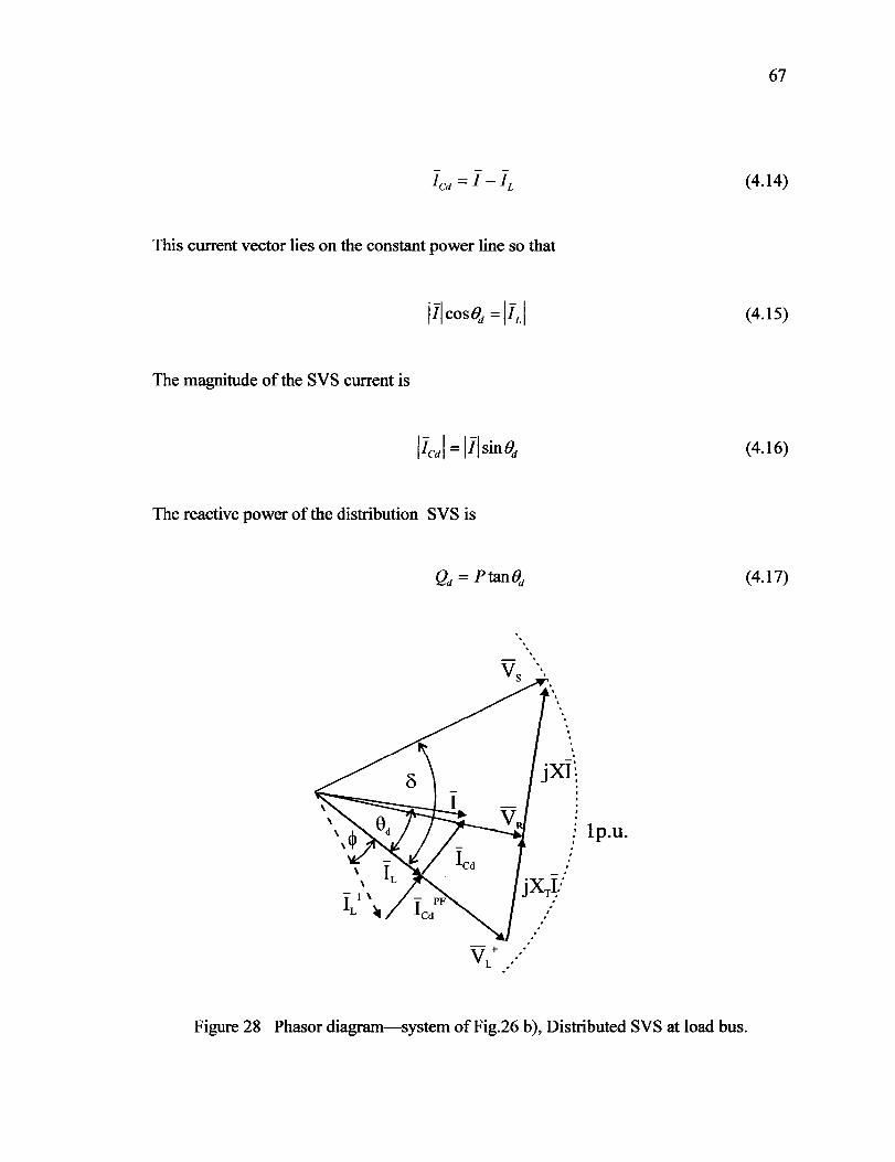
Reproduced with permission of the copyright owner. Further reproduction prohibited without permission.
67
(4.14)
This current vector lies on the constant power line so that
(4.15)
The magnitude of the SVS current is
(4.16)
The reactive power of the distribution SVS is
(4.17)
lp.u.
Figure 28 Phasor diagram-system ofFig.26 b), Distributed SVS at load bus.

Reproduced with permission of the copyright owner. Further reproduction prohibited without permission.
68
4.4.2.1 Load with Lagging Power Factor
Normally the load current lags VL by a power angle cp. Fig. 28 illustrates this case by the
broken line phasor of the load current IL 1. When the load receives the same real power P,
IL 1 must lie along the same constant power locus so that
(4.18)
Therefore in order to correct the lagging power load, the distributed SVS should take
another capacitive current component Ic/F whose magnitude is k 1sincp and whose
direction is the same as led· In this case 1= IL 1 +Icd+Ic/F. The total current of the V AR
compensator isle= Icd+IcdPF.
The V AR required for power factor compensation is
(4.19)
Since the load can have different power factors, the systematic approach is to consider
that QlF is for power factor correction. For the remainder of this chapter, the focus is
placed on Qd = P tan ed, the requirement for voltage support.
4.4.2.2 MV A Rating Requirement of Load Transformers
The voltage rating of the load transformers must be V L + p. u. The load current is IL= 11 V L +.
From (4.15) the magnitude of the transformer current 1 is 1= IL /cos ed. Therefore the
MV A requirement ofthe load transformers is 1 SdLoad 1 =VL+1=1/ cos ed.

Reproduced with permission of the copyright owner. Further reproduction prohibited without permission.
69
4.5. Comparison of MV Ar Requirement of SVS
For comparisons to be meaningful, the same real powers, P=1p.u., are drawn from the
load bus at unity power factor and the load voltage 1 VL 1 = vL+· For distributed svs the
MV Ar is calculated from Qd= P tan8d, where 8dis computed from (4.13). For bulk SVS at
the transmission line voltage VR, Qb = P(tan8b+tany) where eb and 'Y are taken from (4.5)
and ( 4.3) respectively. Ptany compensates jXT of the load transformers and resembles an
overhead requirement irrespective of transmission line length. Ptan8b compensates the
line reactance jX and since X=O.OOI3 x km it increases with the length of the transmission
line.
Fig.29 presents Qd and Qb in per-unitized MV Ar plotted against the line length in km. The
savings Qb-Qd, in adopting distributed SVS in preference over bulk SVS, varies from 5%
to 10%, depending on the length of the transmission line. The 10% corresponds to XT, the
transformer leakage reactance.
0.4 .---.,..---.------.-----,.--.----..,----.-----, 1 1 1 1 1 1 1
!Power :transferred ovtr the liRe= 1 p.u : ..... 0.35 ------:------ ~----- -7------ t----- -:-------:------ J ~ 1 1 1 1
1 1 1 1
~ 0.3 ---B~lk-SV~··Qb~------~------~----._ ~0.25 0 a. ~ 0.2 .B ~0.15
~ 0.1
' o.os -- -- . ---- tiistributed svs:.:Qd----- +--- -- ~------
1 1 1 1 1 1 1
50 100 1.50 200 250 300 350 400 line length [km]
Figure 29 MV Ar (p.u.) requirement of SVS plotted against transmission distance (km). Bulk SVS--Qb; Distributed SVS--Qd. (X=0.0013 1 km, Xr0.10 p.u.)

Reproduced with permission of the copyright owner. Further reproduction prohibited without permission.
70
4.6 Comparison of MV A Requirements of Transformers
For real power, P=l, for distributed SVS, the MV A rating of ail theM load transformers
is 1 Sd Loadl =1/cosed, where ed is computed from (4.13). For bulk SVS, the MV A rating of
ail the M load transformers is 1 sb Loadl =lNL+ with vL+ computed from (4.2). The
additional transformer to step up the voltage of the bulk SVS to transmission line voltage
must have an MV A rating of: 1 Sb svsl =(tan9b +tany) where eb and y are taken from ( 4.5)
and (4.3) respectively.
1 '
0.9 ---- ...... ,_ ... ---- "'1------ .. ------ .. ------,..----- .. , ... -- .. -- .... - - ...... Lo~d Tntnsfonher - DistribtJted s!vs :! 0 8 ______ i ______ j ___ l~~i~~~~i_--.---~------i ______ j_ ----
,......, • 1 1 1 1 1 1 1
::s : :Load Tran~nner:- Bul~ SVS: s o. 7 ------:------ ~------ f---- _o::~,b~b--Lo---~-dl-----,------ 1------< : : : ~- a : :
~ 0.6 ----- -:------ ~------ ~------ ~------ :------ -:------ ~------
1 1 1 1 1 1 1
1 1 ' 1 1 1 1
0.5 ----- -~----- ~------!------ ~----- -~----- _:_----- ~------1 1 1 1 1 1 1
1 1 1 1 1 1 1 1 1 1 1 1 1 1
04 ------~-----J------•------•------~-----~------•------0 Bl)lk Svp ISb~SVSI : : ; :
' ' ' 0.2 ------~-----~-----
1
----~------~-----~------~------' 1 1 1 1 1 1 1 1 1 1 1
50 100
1 f 1 1 1
150 200 250 line length fkm 1
300 350 400
Figure 30 MV A (p.u.) of transformers plotted against transmission distance (km)_ 1 Sb svsl ---transformer connecting Bulk SVS to power system_ Load Transformers: 1 Sb-Loadi--Bulk SVS; 1 Sd-Loadi--Distributed SVS. (X=0.0013 1 km, Xr=O.lO p.u.)
Fig. 30 presents the per-unitized MV A of load transformers: 1 Sd Loadl of distributed SVS
and 1 Sb Loadl of bulk SVS plotted against the line length. Bulk SVS requires its own
transformer of 1 Sb svJ rating. In using distribution SVS, the compensating currents pass

Reproduced with permission of the copyright owner. Further reproduction prohibited without permission.
71
through the load transformers so that their MV A have to increase especially when
transmission line is long.
4. 7 Discussion
4.7.1 Cost of V AR Compensators- Bulk Size vs. Distribution Size
The savings, Qb-Qd, in MV ARs shown in Fig. 29 translate to lower costs in the Static
V AR Compensators or STATCOM and switched capacitors for distributed SVS.
However there is a cost component related to controls. Since every unit has its own
controls, this cost component of distributed SVS increases with M, the number of units.
4.7.1.1 Estimate in Savings
As it is difficult to obtain cost of equipment from manufacturers, the authors have
presented in Table 1, the estimates of savings based on the MV AR of SVS saved
multiplied to $/k.V AR of SVC or STATCOM which have been listed in [69,70]. The
MV Ar saved is based on a conservative estimate of 5% (ta.ken from Fig.29). Cost
estimates for STATCOM and SVC are: STATCOM 50$/k.V Ar and SVC 40$/k.V Ar.
Although the references were dated in 1996, the numbers provide reasonable guidance in
2004.
4. 7.2 Cost of Transformers
In distributed SVS, there is a potential saving because the high voltage transformer of the
bulk SVS of Fig. 26 a) is not required. However, the compensating currents from the
distributed SVS of Fig. 26 b) must still pass through the M load transformers. Therefore
their total MV A rating must be increased as 1 Sd Loadl shows in Fig.30. As the voltage

Reproduced with permission of the copyright owner. Further reproduction prohibited without permission.
72
rating is kept regulated at V L +, it is the current rating which is increased thus requiring
thicker copper windings.
Bulk SVS requires an additional transformer with MV A rating of 1 Sb svsl =(tan9z +tany).
As the transformer carries Qb of the bulk SVS, the plot of 1 Sb sv~ in Fig.30 is the same as
Qd in Fig.29. Not having to pay for a high voltage transformer of this MV A rating is an
important saving knowing that it can make up to 20% of overall cost of SVC [69,70].
However, this has to be compared with the increase in the MV A of load transformers of
distributed SVS. Since reactive power is added vectorially to the real power of the load,
i.e. 1 Sd Loadl =[ 1 +Q/]0·5, the increase only by about 7% for 400 km in Fig.30.
Table 1
Savings from reduced Mvar of SVS
Nominal Voltage 1-1 230 345 500 735 [kV]VsASE [kV] [kV] [kV] [kV]
PsiL = SsASE [MV A] 140 420 1000 2280
savings [pu] 0.05 0.05 0.05 0.05
savings [MV Ar] 7 21 50 114
savings [$] $1.05 $2.5 $5.7 voltage support provided 350000 million million million entirely by STATCOM
savings [$] $4.56 voltage support provided 280000 840000 $2 million million
entirely by SVC
4.7.3 Cost of AC Circuit Breakers
Each SVS has its AC Circuit Breaker. The cost of M Circuit Breakers at distribution
voltage level and each having MVA rating at PM/(M-1)cos91 is to be compared with the

Reproduced with permission of the copyright owner. Further reproduction prohibited without permission.
73
cost of K Circuit Breakers of bulk SVS each rated at PK(tan82 +tany)/(K-1) MV A rating
at transmission or sub-transmission voltage level.
4.7.4 Cost ofRedundancy
In bulk SVS ofFig. 26 b), N-1 reliability criterion requires K SVS for standby. Expressed
in terms ofMV Ar, the cost ofredundancy is KQJ!(K-1)
In distributed SVS, the cost is MQJ(M-1 ).
4.7.5 General Note
It should be noted that VL+ is defined and required for this work only. It fulfils the
function of ensuring that the bulk SVS and distributed SVS are evaluated on equal
footing. In other studies of distributed SVS where comparisons are not needed, the load
bus voltage will be set as VL=l.O p.u. This will simplify Fig. 28 as VL will lie on the unit
circle and ô=28d.
4.8 Conceptual Design of Power Delivery Substation
This section presents the conceptual design example of a 315/25 k V substation receiving
power in the range of 50 MW to 375 MW from a 300 km long, 315 kV line. The desired
voltage profile in the line is: at the sending end 1 Vs 1 =315 kV and at the receiving end at
the 25 kV busses of the substation, the load voltage is regulated at 1 VL 1 =25kV. The
substation load is assumed to be at 90 percent power factor. The SVS units are located on
the 25 kV bus of the substation.

Reproduced with permission of the copyright owner. Further reproduction prohibited without permission.
74
4.8.1 MV AR Requirements of Substation
In the preceding sections, for simplicity in presenting the comparative merits of the
transmission voltage vs. distribution voltage locations of the SVS, the lossless lumped
inductance has been used to model the transmission line. Unfortunately, such a model
cannot predict overvoltages when the load is below the Surge-Impedance Loading (SIL).
In this section, the distributed parameter model is used. As the method is familiar to most
readers, it is necessary only to recall that the single-conductor line is characterized by:
z, impedance per km (z = 0.474 ohm/km, from [71])
y, admittance per km (y= 3.33x10⁻⁶ Slkm, from [71])
Z = z ·1 and Y = y·l, where 1 is the length of the line in km. Zs = J4Y = 3 77 ohms, Vs is
315 kV hence the Surge-Impedance Loading (SIL) ofthe line (= 1 Vs 12/Zs) is 250 MW.
At the receiving end, it can be shown that the real and reactive powers are given by:
(4.20)
(4.21)
where 1 Vs 1 is the sending-end voltage, 1 VRI is the receiving-end voltage, ôis the angle
1 1 1 1 r;;-;; sinh JZY
between Vs and V R , A = cosh v ZY and B = Z JZY .
1~ = 1.256x10⁻³ (300) = 0.377radians = 21.6•
A= cosh/ZY = coshljzy = cos21.6. = 0.9298
ZY
sinh JZY sinh !.foY sin 21.6" B = Z ,-;;;; = zl r:::: = 0.474x300 = 138.85
viT ~zy ~n

Reproduced with permission of the copyright owner. Further reproduction prohibited without permission.
75
Integrating the transmission line equations with the step-down transformer leakage
reactance, the QR required by the transmission line, to meet the voltage constraint
1 Vs 1 =315 k V and 1 V L 1 =25kV at both ends of the line, is shown in Fig. 31 under the
label "Line". Inductive MV ARs are required to counter overvoltage for light loads and
capacitive MV ARs for heavy loads. The cross-over takes place at the Surge Impedance
Loading (SIL) of250 MW.
Before proceeding further, a brief digression is in order. In Section 4.3, mention has been
made that the transformer reactance jXT contributes to the effectiveness of voltage support
when the SVS is on the 25 kV side. This has been demonstrated by the quantitative
comparison appearing in Fig.29 by which the capacitive MV ARs of Distributed SVS is
less than that of Bulk SVS. This raises the question as to whether the transformer
reactance jXT can contribute to reducing the -50 MV AR (inductive) required to prevent
overvoltage when operating under low load condition. In transmitting 375 MW at 0.9 pf,
the MV A base is 375/0.9=416.6 MV A. For 25 kV, it can be shown that the Zbase phase is
0.50 ohm. Assuming that -50 MV AR is provided by jXsvc the inductive reactance of
SVCs, the equivalent value ofXsvc =4.16 or 8.32 pu. The transformer reactance is taken
as XrO.l pu. Therefore, the size ofXsvc can be reduced to (8.32-0.1=) 8.22 pu. As this
reduction is small, it is neglected for the remainder of this chapter.
There is a second requirement for capacitive MV ARs. This is for unity power factor
correction of the loads. For load operating at 0.9 pf, Qprthe capacitive MV ARs required is
shown in Fig.31 under the label "Load". The total MVARs required at the substation is
QrQR+Qpr is shown under the label "Operating range of the SVS". In this chapter the
term ··svs" covers a combination of switched inductor, switched capacitors and power
electronic V AR controllers such as SVSs or STATCOMs.

Reproduced with permission of the copyright owner. Further reproduction prohibited without permission.
300 km line ~r----r----r----r----r----r----r---~
~150
~100 ....... a 5o
.~ ...... u .g -50
·=
: :operatjng range : : ' ' f' ' 1 1 -------:------ -;-- -- -o ~vs--~--~--,-------;---- -1 1 1 1 1 1 1 1 1 1 1
' tpad ------ -(--~------ -1-------:---
1 ~. 1 1 1
~------~------~------ -- ---r-------~------,-------1 1 1 1 1 1
1 ' 1 1 1 1 1 1 1 1 1 1
' 1
:::: 1 t' 1 1 1 1 1 ---- ------------------------ ---------- -------1 1 1 1
' 1 1 1 1 1 1 1 1 1
1 1 1 1 1
-----.-------~-------;-------~-------~------~--- --: : : lide plus itransfoimers
1 1 1 1 -100 L------L-----L------'-----L------'-----L------' 50 100 150 200 250 300 350 400
P r?vfWl
76
Figure 31 Operating range ofSVS. ( requirement for load from 50MW to 375 MW)
4.8.2 Substation
As shown in Fig. 32, the conceptual design of the substation consists of: high-voltage line
terminations, high-voltage busbars, power transformers, low-voltage busbars and law
voltage line terminations. Breaker-and-a-half is used for both voltage levels main-buses in
order to fulfill the reliability of power supply. Three 125 MW power transformers are
èhosen for the total power of 375 MW. One spare transformer is also used to increase the
reliability. The total power distribution at 25 kV level is divided by 4 buses, each is
around 125 MW. Each bus has one SVS with five terminations of25 MW each. The SVS,
located on the 25 kV bus of the substation, control the reactive power (unity power factor)
so asto regulate the bus voltage at 25 kV.
Reproduced with permission of the copyright owner. Further reproduction prohibited without permission.
77
4.8.3 Rating of Transfonners
The 181 MV AR capacitive required for power factor correction does not cross the
transformers. Thus the transformers must be rated to carry the maximum real power of
375 MW and the capacitive reactive power OR =60 MV AR ( according to Fig. 31 ), which
is required to support the receiving end voltage of the transmission line from dropping.
The total MV A of the transformers should be (3752+602)0
·5=379 MV A. In choosing 3
transformers, the MV A required for each is 127 MV A. For (N-1) reliability, 4
transformers, each rated at 125 MV A, are chosen in the substation layout as illustrated in
Fig.32.
Figure 32 Single Line Diagram for 315/25 kV, 375 MW substation
4.8.4 Rating of SVS
From Fig. 31, the total MV AR requirement of the SVS ranges from -50 MV AR
(inductive) to 240 MV AR ( capacitive) ( 60 MV AR for voltage support + 180 MV AR for pf
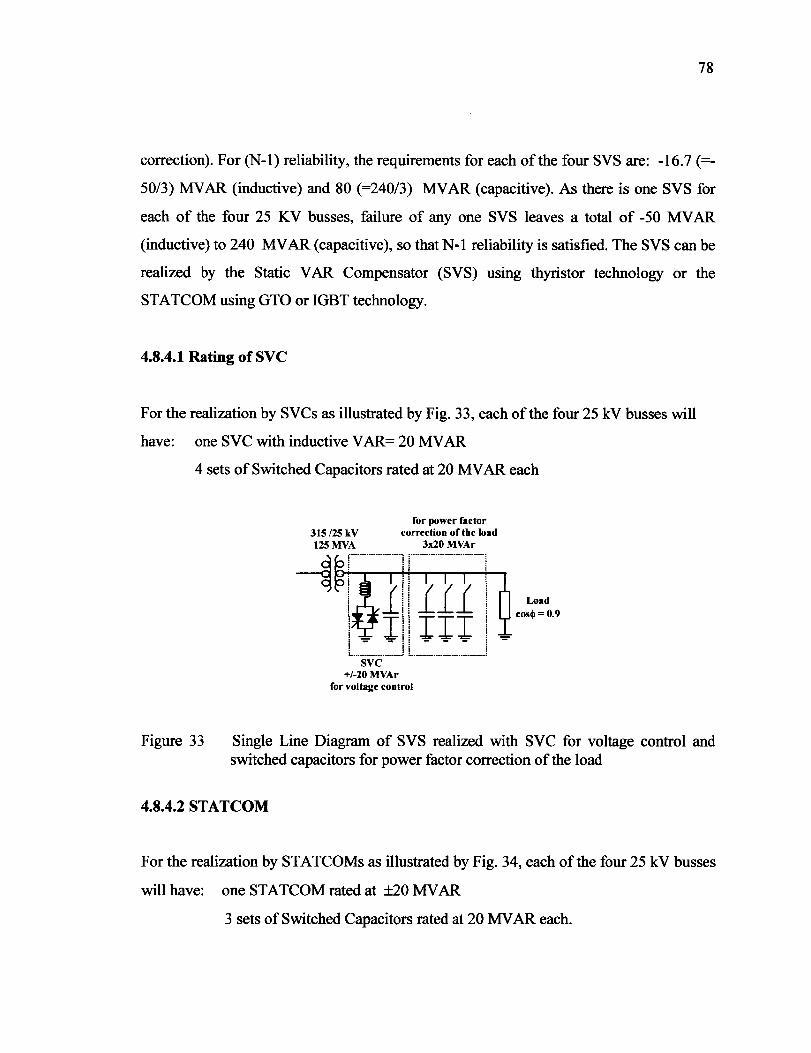
Reproduced with permission of the copyright owner. Further reproduction prohibited without permission.
78
correction). For (N-1) reliability, the requirements for each of the four SVS are: -16.7 (=-
50/3) MV AR (inductive) and 80 (=240/3) MV AR (capacitive). As there is one SVS for
each of the four 25 KY busses, failure of any one SVS leaves a total of -50 MY AR
(inductive) to 240 MY AR ( capacitive ), so that N 5 1 reliability is satisfied. The SVS can be
realized by the Static V AR Compensator (SVS) using thyristor technology or the
STATCOM using GTO or IGBT technology.
4.8.4.1 Rating of SVC
For the realization by SVCs as illustrated by Fig. 33, each of the four 25 kY busses will
have: one SVC with inductive V AR= 20 MV AR
4 sets of Switched Capacitors rated at 20 MY AR each
Figure 33
315/25 kV 125MVA
for power factor correction of tbe Joad
3x20MVAr
svc >t/-20MVAr
for voltage control
Load cos<!l = 0.9
Single Line Diagram of SVS realized with SVC for voltage control and switched capacitors for power factor correction of the load
4.8.4.2 STATCOM
For the realization by STATCOMs as illustrated by Fig. 34, each of the four 25 kV busses
will have: one STATCOM rated at ±20 MY AR
3 sets of Switched Capacitors rated at 20 MY AR each.

Reproduced with permission of the copyright owner. Further reproduction prohibited without permission.
315/25 kV 125MVA
for power factor correction orthe Joad
Jx20 MVAr
~~ ~liil STATCOM T' ! III +/-20MVAr = ! = = =
for voltage control L. _________________ _
79
Q ~·· = cos+=0.9
Figure 34 Single Line Diagram of SVS realized with ST ATCOM for voltage control and switched capacitors for power factor correction of the load
4.9 Dynamic Performance
As the preceding analysis is meaningless if the distributed SVSs will interact adversely
against each other during transients, simulations studies have been performed which
should put to rest such concem. The simulations have been carried out using HYPERSIM
[72], a real-time simulator based on parallel computers developed by Hydro-Quebec. The
value of HYPERSIM in cornes from the availability of default models of transformers,
induction motors and transmission lines ( distributed line inductance and capacitance)
based on many years experience of Hydro-Quebec researchers. All models are very
accurate of high order. The real-time capability of HYPERSIM is not important in the
simulations carried out.
The system which has been simulated consists of system from Fig. 32 which is connected
to an infinite bus by a 300 km long 315 kV line. The power transferred over the line is
3 7 5 MW. Half of the load is resistive. The other half is induction mo tor driving constant
torque load ( compressor load of air-conditioning and refrigeration). The SVS is based on
STATCOMs. Each STATCOM has its own control circuit. Only local feedback is used.
Fig. 35 shows the case ofthe sudden loss ofSTATCOM #2 in the system ofFig. 32. The
simulated instantaneous voltages at each ac bus have been converted to RMS voltages and
displayed in Fig. 35 a) against the reference voltages. The waveforms show that the

Reproduced with permission of the copyright owner. Further reproduction prohibited without permission.
80
transients disappear within 0.05s and the maximum voltage deviation is only about 0.1 kV
(0.7% of rated 25 kV). Fig. 35 b) records the simulated instantaneous phase currents of
the STATCOMS which lead the phase voltages by 90°. The sudden loss ofSTATCOM #2
is apparent in the disappearance of the current. The other three ST A TC OMs respond by
increasing their currents to make up for the lost one. The simulation clearly shows that
any fear that instability arising from the STATCOMs interacting adversely with each
other is groundless.
Phase voltages RMS values [kV] > 14.6 .----,-----..-==-----r----r--=--....=------, =. v; 14.4 ( fi ) :::J VoHage V re erence ~
14_2
VoHage V bus 1 0 0.05 0.1 0.15 0.2 0.25 0.3 > 14.6 .----,.-----.----.,.-----.,.-----.-------,
.x
';: 14.4 "~ ~ VoHage V b / 2 Voltage Vb .. s 2(reference) > 14.1 us ''f'
0 0.05 0.1 0.15 0.2 0.25 0.3 > 14.6 .----,----.----or----.-----.-------, .x
~ 14.4 /~ ~. VoHage V VoHage Vb .. s a<reference) > 14_2 bus 3 ''f"
0 0.05 0.1 0.15 0.2 0.2.5 0.3 > 14.6 .------,-----.-----r----.-----.-------, .x
:14.4 /~ ~ VoHage Vb 4 VoHage Vbus 4(reference) > 14.2 us
0 0.0.5 0.1 0.1.5 0.2 0.25 0.3
timc [sec]
Figure 35 a) Phase voltages of25 kV bus ofFig.32 when STATCOM #2 is lost
Fig. 36 shows the case of the sudden disconnection of one load bus as happens when its
èirèuit breaker trips. Fig. 36 a) shows RMS values of phase voltages of supported buses.
Fig. 36 b) shows phase-a current of every STATCOM. The lowest trace on Fig 36 b)
shows power transferred over the transmission line. Once again, the results demonstrate
that the STATCOMS operate harmoniously.

Reproduced with permission of the copyright owner. Further reproduction prohibited without permission.
81
STATCOMs phase a voltages and currents :s:rA:_rc _ _1 _ _. _ _ ~ _ _ _ _ _ _ _
fW\Yl\lf:\Yl\Yl\lf:\Yl\Yl~\Jl\7';\Yl\Yl~\Yl\Jl~ -2 1 ' 1 1
.,.... 0 O.OS O.l 0.1.5 O.l O.lS 0.3
~ 2
o~-- c- - - -· ,~1\~î\~~i\-1\~1\~~~~1\~1\~~h-n-n~-> _ _ . _ . tl~_ .-v_ tL tt tL _tl tL
_2 ' la · Va• · , ...... 0 O.Ol 0.1 O.ll 0.2 O.ll 0.3
~ :s:rA:_rc _ _3 _ _, _ _ _ _ _ _ _ _ _ _ _
~\YI_ \Il ~\Yl "f~l";\Jl\Yl ~\Yl\Jl \J1\Yl \Jl\f1 -2~----~----~--~~----~----~----~
0 O.Ol 0.1 O.ll 0.2 0.2l 0.3
:_T_C•~-~- --• fWl\Yl\Yf\Yl\Yl\Yf\Jl\Yl~~\Yif\Yl\Yl~\Jl\Jl\f1 -2~----~----~----~~~~----~----~
0 O.Ol 0.1 O.ll 0.2 0.2l 0.3
timc [sec J
Figure 35 b) Voltages and current of one phase of every STATCOM ofFig.32. Current disappears when STATCOM #2 is lost (Qbase= 25 MV Ar)
Phase voltages RMS values [kV]
~ .::~ : ' : l (/)
::J .n > 14
0 0.2 0.4 0.6 0.8 1
~ .::~ : : ' 1
N .., ::J
..0 > 14
0 O.l 0.4 0.6 0.8 1
> .::~ :
' '
1
=. (1) (/)
::J .n > 14
0 O.l 0.4 0.6 0.8 1
> .::~
: ' ' 1
=. ...,. (/)
:3 .n > 14
0 O.l 0.4 0.6 0.8 1
timc [sec.]
Figure 36 a) Phase voltages (rms) of25 kV bus ofFig.32 when circuit breaker trips thus disconnecting load and STATCOM #2.

Reproduced with permission of the copyright owner. Further reproduction prohibited without permission.
:·)IÎ#;;J~i!~~ ~·-:M ·~ ·~ ·~ ·~ i ~·-:~ 10 0.2 0.4 0.6 0.1 1
~·-m -1L---------------------L-----~------~------L------J -~ :rs:; ·:· ·~ ·~ i 0 0.2 0.4 0.6 0.1 1
timc [sec.]
82
Figure 36 b) Phase-a current of every STATCOM. The lowest trace shows the power transferred over the transmission line.
4.9.1 Bulk vs Distributed SVS
Fig. 37 repeats the simulations of Fig. 35 with the important difference that ali the
distributed STATCOMS are lumped together as a single bulk STATCOM (as would be
used if the compensation is on the high voltage side without satisfying the N-1 reliability
criterion). After the sudden loss of the STATCOM, ali the load bus voltages drop
instantaneously for about 15 % as shown in Fig. 37 a). Fig.37 b) shows the phase-a
current of the STATCOM, the reactive power flow of the load substation, the induction
motor power and the induction motor slip (lowest trace). As the load has a large induction
motor component, the large inductive var causes the load bus voltages to continue
dropping as are evident from the graduai descending slopes in Fig. 37 a). This is because
the lowering of the terminal voltage slows the induction motors further, increasing their
slip and inductive var, as shown in Fig. 37 b). The positive feedback aggravation

Reproduced with permission of the copyright owner. Further reproduction prohibited without permission.
83
eventually leads to voltage collapse. Fig. 37 shows that when bulk SVS is used on the
high voltage side, N-1 reliability criterion requires at least 2 units.
Phase voltages RMS values [kV)
: ::B : : : : l 0 0.2 0.4 0.6 0.1 1
1 ::B : : : : l 0 0.2 0.4 0.6 0.1 1
i ::b : : : : J 0 0.2 0.4 0.6 0.1 1
f ::b : : : : J 0 0.2 0.4 0.6 0.1 1
time [sec.]
Figure 37 a) Phase voltages (rms) of25 kV bus when single bulk STATCOM providing voltage support to 315 k V bus is lost
~ :~-: -: -: -----!] -5~----~-------L------J-------~----~
0 0.2 0.4 0.6 0.8 1
Figure 37 b) Phase-a current of bulk STATCOM, reactive power flow through the substation, active power drawn by the induction motor and motor slip

Reproduced with permission of the copyright owner. Further reproduction prohibited without permission.
84
4.10 Conclusion
The preliminary evaluation, based on: (1) savings in MV Ars required of the SVS and (2)
savings in MV As of the transformers, has shown that distributed SVS is more
advantageous than bulk SVS located at the transmission line bus. Saving from the cost of
reduced redundancy to meet N-1 reliability criterion will require knowing K, the number
of SVCs or STATCOMs for standby, which will be used for bulk SVS. The designers of
bulk SVS willlikely divide the installation after the pattern ofFig.4.8.
Preliminary transient studies have demonstrated that the many SVS units operate
harmoniously together. From the positive conclusions, further in-depth studies are
justified. These studies will identify unforeseen problems in load centers regulated by
distributed SVS and solve them when they surface.
Reproduced with permission of the copyright owner. Further reproduction prohibited without permission.
CHAPTERS
DISTRIBUTED, DISTRIBUTION STATIC V AR SYSTEMS VS. LUMPED
STATIC V AR SYSTEMS: AN IN-DEPTH STUDY
5.1 Introduction
In the previous chapter it has been shown that, when a load center requires SVS for
voltage support, the strategy of using many smaller sized SVS located at distribution bus
is advantageous over lumped compensation on transmission level. In this chapter a step
further is made toward generalization of the proposed concept showing that, when a few
load centers are in parallel, providing voltage regulation with many smaller sized widely
distributed Static V Ar Systems (SVSs) at distribution level has more advantages than a
few large lumped SVSs on transmission level. The benefits obtained from distributed,
distribution voltage support scheme are quantified. The feasibility and reliability of
distributed voltage support scheme with SVSs based on SVCs and STATCOMs are
demonstrated by detailed real time dynamic simulation.
The structure of the chapter is as follows: Section 5.2 describes general system model
used later in the chapter for steady state analysis. Section 5.3 demonstrates the feasibility
of distributed, distribution voltage support scheme using phasors, while in section 5.4,
reliability of distributed voltage support is demonstrated. In Section 5.5, SVS rating of
distributed, distribution voltage support is calculated and compared to the rating of
lumped SVS put on the transmission side of the power delivery substation. To calculate
the rating, distributed line parameters have been used. In Section 5.6 a rough estimate of
the cost of two compensation methods and their impact on line losses is addressed.
Section 5. 7 compares steady state loadability limit for two compensation schemes and,
fmally, in Section 5.8 detailed real time dynamic simulation of a test system is perfonned.

Reproduced with permission of the copyright owner. Further reproduction prohibited without permission.
86
5.2 System Model for Voltage Support Analysis -
In this chapter, more general model is considered consisting of K incoming transmission
lines serving N equal constant power loads.
Fig.38 illustrates the case when voltage support is provided by N distributed SVSs
installed on distribution side of power delivery substation. Fig. 39 îllustrates the case
when one lumped SVS provides voltage support on transmission side of the power
delivery substation. SVS is treated as continuous source of reactive current. It consists of
switched capacitors (for economy reason) in combination with STATCOM or (Thyristor
Control Reactor) TCR. Distributed parameters are used to model each line. Resistive
losses are neglected.
Figure 38 Single line diagram of K incoming transmission lines serving N loads over N transformers each having reactance jXT. Each load is provided with its own SVS providing voltage support on distribution side of power delivery substation ( distributed compensation).

Reproduced with permission of the copyright owner. Further reproduction prohibited without permission.
1 V i1; Vu Îu 1---......!:..,..__~•~-----t--glS lload•
-I
K transmission lines
-I .,
step up
transformer i lumped svs
~ L2 !L2
_load
VLN I 1 _.LN
load
87
Figure 39 Single line diagram of K incoming transmission lines serving N loads over N transformers each having reactance jXT. Voltage support is provided with one lumped SVS on transmission side of substation .
5.3 Feasibility
Before proceeding to make comparisons, it is necessary to establish that voltage support
by distributed V AR compensation is mathematically feasible. This means that there are
steady-state solutions for the conditions of operation. The steady-state solutions are
presented here in the form of phasor diagrams. For the sake of the clarity, the number of
distribution circuits is restricted to N = 3, and loads are assumed unity power factor
(power factor is corrected).
5.3.1 Non-Compensated Line
The phasor diagram in Fig.40 presents the steady-state voltages and currents for non
compensated line where the number of loads is N = 3. The sending end voltage Vs is kept
at 1 p.u. due to stiffness of the system. The current 1 = lu+IL2+1u through transmission
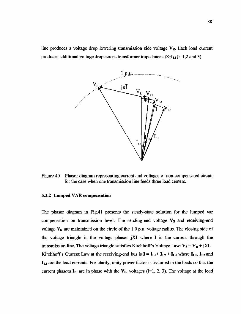
Reproduced with permission of the copyright owner. Further reproduction prohibited without permission.
88
line produces a voltage drop lowering transmission side voltage V R· Each load current
produces additional voltage drop across transformer impedances jX du (i= 1 ,2 and 3)
Figure 40 Phasor diagram representing current and voltages of non-compensated circuit for the case when one transmission line feeds three load centers.
5.3.2 Lumped V AR compensation
The phasor diagram in Fig.41 presents the steady-state solution for the lumped var
compensation on transmission level. The sending-end voltage Vs and receiving-end
voltage VR are maintained on the circle ofthe 1.0 p.u. voltage radius. The closing side of
the voltage triangle is the voltage phasor jXI where 1 is the current through the
transmission line. The voltage triangle satisfies K.irchhoff's Voltage Law: Vs= VR + jXI.
Kirchhoff's Current Law at the receiving-end bus is 1 = lu+ lu+ lu where lu, lu and
ILJ are the load currents. For clarity, unity power factor is assumed in the loads so that the
current phasors ILi are in phase with the Vu voltages (i=l, 2, 3). The voltage at the load

Reproduced with permission of the copyright owner. Further reproduction prohibited without permission.
89
bus i is Vu=VR- j XT lu, for i=1, 2, 3. It is apparent from Fig.41 that while VR is
regulated, Vu, VL2 and Vu are not.
Figure 41 Phasor diagram for circuit from Fig. 39 showing voltage support from lumped compensator Compensating current le, injected in quadrature with voltage VR.
5.3.3 Distributed V AR Compensation
The phasor diagram in Fig.42 presents the steady-state solution for the distributed var
compensation ofFig.38 for N=3. It shows that even when the load currents lu, IL2 and lu
are not equal (evident in the phasorsj XT lu, for i=1, 2, 3 zoomed in Fig.42), the load bus
voltages Vu, VL2 and Vu can be regulated at 1.0 p.u. The receiving-end bus voltage VR
has a voltage lower than 1.0 p.u.

Reproduced with permission of the copyright owner. Further reproduction prohibited without permission.
Figure 42
·--..
\ \
.......... ... ... ....... ~-~- . -~~- --- ........ -........ ~
\ \
\
/ ! /
i
\ ' \
1 /
90
Phasor diagram for circuit from Fig. 38 showing voltage support from distributed compensators (SVSs or DSTATCOMs). Each SVS injects compensating current ICi (i=l,2 and 3), in quadrature with voltage it supports

Reproduced with permission of the copyright owner. Further reproduction prohibited without permission.
91
5.4 Reliability
The loss of lumped SVS in Fig.39 (disappearance of current le on phasor in Fig.41)
affects allload centers and can lead to voltage collapse. To satisfy N-1 reliability criterion
there must be another stand by unit rated at the full MV Ar required by the system. The
loss of one of the smaller sized distributed, distribution level SVS affects only the load
center that has been supported by the lost SVS and, partially, receiving end transmission
voltage VR. However, the other distributed SVSs will indirectly support transmission
voltage V K and voltage on the bus where SVS has been lost.
Fig.43 describes the loss of SVS regulating load bus voltage Vu. Its loss makes
compensating current le3 equal to zero. As a consequence, the line current 1 decreases and
rotates. The voltage Vs is kept at 1 pu due to stiffness of the system. Vector jXI
(representing line voltage drop) rotates, decreasing voltage VRon transmission side of the
substations. Due to decrease in Va. distribution side voltages (load voltages) Vu (i=1,2,3)
sag. The sag of voltage Vu is biggest because the SVS regulating it is lost. Control
system of SVSs providing voltage support of load bus voltages Vu and Vu detect their
decrease and act fast in order to restore them at 1 pu. The compensating currents let and
Ic2 increase becominglc1NEW and lczNEw,respectively, (new SVSs compensating currents)
providing additional voltage boost. The line current 1 increases rotating voltage drop jXI.
This increases transmission voltage V R but not on the same level as before the loss of the
SVS, increasing load bus voltage V Ll· The voltages Vu and Vu are restored at 1 pu.
Voltage Vu stay depressed, but it is indirectly supported due to increase in transmission
voltage VR. New steady state solution is shown in Fig.43. It is clear that the loss of one
distributed SVS can be partially mitigated by the action of the other SVSs those stay into
the system.
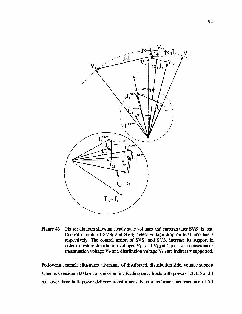
Reproduced with permission of the copyright owner. Further reproduction prohibited without permission.
92
Figure 43 Phasor diagram showing steady state voltages and currents after SVS3 is lost. Control circuits of SVS1 and SVS2 detect voltage drop on busl and bus 2 respectively. The control action of svsl and svs2 increase its support in order to restore distribution voltages Vu and Vu at 1 p.u. As a consequence transmission voltage V R and distribution voltage Vu are indirectly supported.
Following example illustrates advantage of distributed, distribution side, voltage support
scheme. Consider 100 km transmission line feeding three loads with powers 1.3, 0.5 and 1
p.u. over three bulk power delivery transformers. Each transformer has reactance of 0.1
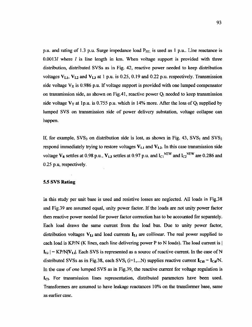
Reproduced with permission of the copyright owner. Further reproduction prohibited without permission.
93
p.u. and rating of 1.3 p.u. Surge impedance load PsiL is used as 1 p.u .. Line reactance is
0.0013/ where 1 is line length in km. When voltage support is provided with three
distribution, distributed SVSs as in Fig. 42, reactive power needed to keep distribution
voltages Vu, Vu and VLJ at 1 p.u. is 0.25, 0.19 and 0.22 p.u. respectively. Transmission
side voltage VR is 0.986 p.u. If voltage support is provided with one lumped compensator
on transmission side, as shown on Fig.41, reactive power Q1 needed to keep transmission
side voltage Vy at lp.u. is 0.755 p.u. which is 14% more. After the loss ofQ, supplied by
lumped SVS on transmission side of power delivery substation, voltage collapse can
happen.
If, for example, SVS3 on distribution side is lost, as shown in Fig. 43, SVSt and SVS2
respond immediately trying to restore voltages Vu and V L2· In this case transmission si de
voltage VR settles at 0.98 p.u., VLJ settles at 0.97 p.u. and let NEw and lc2NEw are 0.286 and
0.25 p.u, respectively.
5.5 svs Rating
In this study per unit base is used and resistive losses are neglected. Ail loads in Fig.38
and Fig.39 are assumed equal, unity power factor. If the loads are not unity power factor
then reactive power needed for power factor correction has to be accounted for separately.
Each load draws the same current from the load bus. Due to unity power factor,
distribution voltages VLi and load currents ILi are collinear. The real power supplied to
each load is KP/N (K lines, each line delivering power P toN loads). The load current is 1
ILi 1 = KP/NIVLïl· Each SVS is represented as a source of reactive current. In the case ofN
distributed SVSs as in Fig.38, each SVSi (i=l, ... N) supplies reactive current ledï =le~.
In the case of one lumped SVS as in Fig.39, the reactive current for voltage regulation is
le1• For transmission lines representation, distributed parameters have been used.
Transformers are assumed to have leakage reactances 10% on the transformer base, same
as earlier case.

Reproduced with permission of the copyright owner. Further reproduction prohibited without permission.
94
5.5.1 Per Unit Normalization
Ali quantities in Fig.38 and Fig.39 are normalized according to Table II so that results are
general and valid for different voltage levels.
Table II
Per unit normalization
Nominal Voltage 1-1 230 345 500 765 [kV]VsASE [kV] [kV] [k. V] [kV] PsiL = SsASE [MW] 140 420 1000 2280
ZsASE = VJ. sAS FI 377.8 283.4 250 256.6 SsASE =Zef Ohm 1
Naturalload PsiL is 1 (p.u.). Pmax = MPsiL = M (p.u.) is maximum power to be transferred
over one transmission line. Bulk power delivery transformer impedance is assumed to be
10% on the transformer base. In case of one incoming line, one substation, XT = 0.1/M
(pu). In case of K incoming transmission line - N outgoing distribution circuit, XT =
O.lNIMK(pu). Transformer reactance changes with transformer rating. The load is
assumed to be constant power. In case of K incoming lines - N outgoing distribution lines
serving N loads, Ru= NIVLïi2/PK (pu) when distribution voltages V Li (i=l,2 ... N) are kept
at lpu and the power transfer over each line is assumed to beP p.u. Total power supplied
to load with K transmission line is then KP p.u. The totalload equivalence, as in Fig.44 a)
and 44 b), is R= IVLI2/PK. When voltage support is provided on distribution side as in
Fig.44 a), IVLI = lp.u. and load R=1/KP. When voltage support is provided on
transmission side as in Fig.44 b ), the distribution voltage IV LI is calculated from Fig.44
b). In this case the load current IL =KPNL. Hence applying Kirchhofl's laws on circuit in
Fig. 44 b), Va=j(XTIKM)IL+ VL:

Reproduced with permission of the copyright owner. Further reproduction prohibited without permission.
95
Figure 44 a) Single line diagram with N loads of Fig.38 equivalenced as a single load carrying current IL. Distributed SVS located at a load bus of V L.
HV ~transformer 'f+ÏCI
Figure 44 b) Single line diagram with N loads of Fig. 39 equivalenced as a single load carrying current k. Lumped SVS connected to bus of Va by additional step up transformer.
(5.1)
solving (5.1) and choosing appropriate solution
(5.2)
Therefore, for constant power load:

Reproduced with permission of the copyright owner. Further reproduction prohibited without permission.
96
R = lvLI2 = !v;J M2 + ~~v~J M4- 4M2 p2 x: KP 2KPM2 (5.3)
Transmission lines are assumed lossless, therefore:
Z'= jZc sinpl (5.4)
Y' . 1 Pl -=J-tn-2 Zc 2
(5.5)
Where, p = (j).J L' C' is wave number and l is line length in km and Zc is line characteristic
impedance. When normalized, (5.4) and (5.5) become (5.6) and (5.7), respectively:
5.5.2 svs Rating
Z'(p.u.) = jsinpl
Y' fJl -(p.u.) = jtn-2 2
(5.6)
(5.7)
When lumped SVS provides voltage support, as in Fig.44 b ), its objective is to keep
transmission voltage VR at 1 p.u. Then, the distribution side voltage has to be regulated,
additionally, by other means. When voltage support is provided on distribution side of
power delivery transformer as in Fig.44 a), distribution si de voltage V L is regulate at 1
p.u. and transmission side voltage does not have to be additionally regulated.
Applying Kirchhoffs laws on circuits in Fig.44 a) and 44 b) under the above cited
conditions, following results are obtained:

Reproduced with permission of the copyright owner. Further reproduction prohibited without permission.
97
5.5.2.1 Lumped Compensation
Reactive current provided by lumped SVS, needed to keep transmission voltage VR at lpu
in Fig.44 b ), is given by:
tn( p z) - ~ 1-( p sin(p l) r J 2 sinpl
(5.8)
Reactive power of lumped SVS is given by:
(5.9)
Where IV Ri= 1 pu.
Distribution side voltage IVLI is obtained from (5.2) knowing that IVRI=lpu and is given
by:
ivLI = M 2 + ~M4 - 4M2 P 2Xi
2M2
5.5.2.2 Distributed Distribution Compensation
(5.10)
The magnitude of reactive current provided by distributed SVSs on distribution side of
power delivery transformer in Fig.44 a) is given by:
P2
( (Pl) x x )2
1 - îVJ sin(P l)tn 2 A7- sin(P 1)- A7 sin(pz) + ~ - sin(pz)m(~1) ~ led= K X (Pl) X - K
sin(pz) + ~ - sin(pz)tn 2 ~
(5.11)
The reactive power needed for distribution voltage regulation is:
(5.12)

Reproduced with permission of the copyright owner. Further reproduction prohibited without permission.
98
The complete derivations of equations (5.8) and (5.11) are given in the Appendix B. The
equations (5.8) and (5.11) are general. They apply to ali voltage levels, power transferred
over the line, and line lengths. Fig. 45 a) to 45 e) show ratings of lumped SVS and
distributed SVS plotted against line length in km for different ranges of power transferred
over the line. Distribution side voltage VL is regulated at 1 p.u. with distribution,
distributed SVS. When voltage support is provided on transmission side of power
delivery substation, transmission voltage Vais kept at 1 p.u. The reactive power needed
for load power factor correction has to be accounted for separately. Fig.45 shows how
reactive power needed for voltage support varies as function of line length and power
transferred over the line.
00.1j ----- "'i'"'--- ...... ï"'---- ... ï--- ... -- ï ----- -;- -- ...... "ï'"'--- .. - i'"' ...... --- i
> 91"- :1 p :: p ~ p : 1 1 1 ·,::: ~ : • ..,. : SIL
··ü o_t r---r=::t:~;==F===f==p=~=~ ::Sœ 1 ·g.
g.œ 0'00_0.5
. . . 1 1 1 1 1
1 Qd 1 • • • 1 1 1 1 1 ----7--- -~----- -:------ ~------ ~ 1 1 1 1 1
1 1 1 1 :p : : : -.. -- --:--- ... -- ~-- ... --- ~ --- -.. -... - ... --~ ~ -:- ----- ~-- -- -- ~ 1 t : ___.,.,.., 1 1 .... 'fr.. 1 1
: : QI --r- : 1 0..1p: : -- .. ---:----- .. -:------7------t------:- ---:- .. --~----1
1 ' 1 1 1 1 1 1 1 1 1
1 • 1 1 1 1
.................. ~ .............. , .................. ~ .................. T"'"'"'"'"'"'~"'"''"'"'"'~"'"'"'"'"'
1.50 lOO 2.50 300
line length [km]
Figure 45 a) Reactive power in p.u. is plotted against line length. The power supplied to load centers vary from 0.3 p.u. to 1 p.u., with unity power factor.
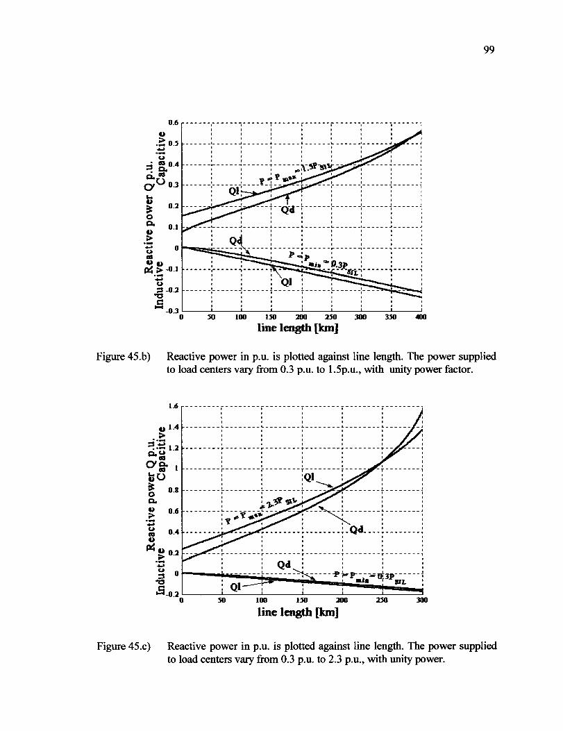
Reproduced with permission of the copyright owner. Further reproduction prohibited without permission.
0.6
Q
.::: 05 .... ·-u :i ~ 0.4 c:i,CIIS
CYU 0.3
t ~ 0 o. Q ..,. ·--u CliS
0.1
0
OQ ~..,. -0.1 ·-.... u
:S -O.l "0 c
-------------------------------------------------------1 1 t 1 1 1 1 1
1 1 1
------1------~------~------~------L-----~------J 1 1 1 1 1 1
---:- -qd-:------:------ -:------:------: 1 1 1 1 1 1
1
------~-----~------1------t------~-----~----
- -0.3 L_ __ .__ __ .~.-__ J._ __ ...L_ __ ...L_ __ ...~-__ ....L __ __J
0 100 uo 200 no 300 llO 400
line length [km]
99
Figure 45.b) Reactive power in p.u. is plotted against line length. The power supplied to load centers vary from 0.3 p.u. to 1.5p.u., with unity power factor.
1.6
Q 1.4 ..,. ··-=!.~ 1.2
o,u CliS
0'~ tu ~ 0 o.
0.8
0.6
--------;--------;--------.--------,--------.--------i
1 1 f 1 1
--------~--------~--------~--------~--------~--1
1 1 1 1 1 --------r--------r--------i·-------ï-----
:QJ t 1 : ~ --------;--------;--------i-----
1 - 1 1 '}.., .. ~\. 1 1 1
--------~ --~v ~.-!- -- -- ; ---' -~ --------t --------j ."Y 1 1 ~ 1 1
~--------~--------~-Cld----~--------: 1 1 1 1 1
1
1
1 1 1 1 1 1
---r--------~--------T--------T--------T--------1
300
Figure 45.c) Reactive power in p.u. is plotted against line length. The power supplied to load centers vary from 0.3 p.u. to 2.3 p.u., with unity power.

Reproduced with permission of the copyright owner. Further reproduction prohibited without permission.
lJ ------------,-------------r------------~-------------1 . . . . 1~ ------------~-------------~------------~-------------
~ ~ 1.4 o..-... O"'ü 1.2 ""co ua. ~0 ~ 0.8
0> ·.::::; 0.6 u CIO
~ 0.4 u
. . . . . . ------------~-------------~------------~-------
1 1 1 . . . . . . ------------~-------------:~ï----------~
1
. 1 •
~-----~-------------~
1 Qd : : ----·------------~-------------~ • • 1
1 1 t 1 1 1 f 1
-------------1------------J-------------J . . . 1 1
.::: 0.2 --------- -:- -------- --- -.;.------ ------ -:-- --- ... ----- -- 1 t: 1 Qd 1 1 1
1 1
~~:[======::::; ~-~~~~~=--~-=-~-=~-!~-~-~-=--=~=--=-~=a~=-~~~~=4=-l=P~--~-~-=--=-==-j 0 100 uo 200
tine length [km]
100
Figure 45.d) Reactive power in p.u. is plotted against line length. The power supplied to load centers vary from 0.3 p.u. to 3 p.u., with unity power factor.
3 ------------~-------------i------------~--------------
2.~
:i u . ;;. C.·_;:: CY"ü 2
L. co u a. ~ üu 0 a. u 0> ·-... u co u 05 ~
1 1 1 1 •
____________ J _____________ l------------~-----------0 • 1
1 1 1 •
• 1 1
------------~-------------r------------~------1 1 • • 1 1 • 1 •
1 •
' 1 ------------,-------------r----- ---' .
-Qet 1
------------~-------------,
1
~-------------·------------~-------------1 1 • 1
~ : Qd 1 1 1
Figure 45.e)
"i: or-------~~~~~~~--~~~~~~~-~-~-~-~-~-~--~-~-~-~-~-· P -:P . -0.3P • -6 : ••• SIL : QI c . 1
~~-~o~--------~~L----------.~ooL----------.~~----------~200
line length [km]
Reactive power in p.u. is plotted against line length. The power supplied to load centers varies from 0.3 p.u. to 3.5p.u. with unity power factor.

Reproduced with permission of the copyright owner. Further reproduction prohibited without permission.
101
Table III
Reactive power requirements for voltage support when voltage support is provided on transmission side (TS) and on distribution side (DS)
line position maximum power transferred over !7.l length the line LP.u.] PsiL =1p.u ~ [km] 1.5 2.0 2.5 3.0 3.5 E
100 TS 0.23 0.4 0.6 0.84 1.12 ~ ·-;:j DS 0.18 0.32 0.5 0.72 0.995 t:r Cl)
200 TS 0.32 0.62 1.02 1.57 2.38 1-< 1-<
~ DS 0.28 0.57 0.98 1.6 2.91 0 300 TS 0.42 0.92 1.83 A - -Cl)
DS 0.39 0.93 .::: - - -- 400 TS 0.55 ~ - - - -Cl) 1-<
DS 0.56 - - - -
The results shown in Fig.45 indicate that there is a point beyond which voltage support on
distribution side becomes less efficient in terms of vars than voltage support on
transmission side. When compensator needed for absorption of reactive power, it is
always more efficient to put it on distribution side.
5.6 Cost of Compensation
5.6.1 Cost of Mvars
The cost of compensation depends on compensation equipment used, overrating
capability of compensation equipment, power transferred over the line, line length, line
parameters, level of competition and overall economical situation. Cost estimates for
STATCOM, SVC and Mechanical Switched Capacitors (MSC) are given in [69,70] are
50$/k.Var, 40$/kV Ar and 8$/kV Ar, respectively. Table IV shows the difference in dollar
value between two compensation methods for 500 kV line for different compensation

Reproduced with permission of the copyright owner. Further reproduction prohibited without permission.
102
equipment used. Savings are calculated as difference between vars required to keep
transmission side of substation voltage VR at 1 p.u when compensator installed on
transmission side of substation and vars required to keep distribution side of substation
voltage VL at 1 p.u. with compensator on distribution side of substation multiplied by
dollar value of MY Ar. These cost estimates are based on 1996 data. Here, they are given
as a guidance only. Only the manufacturers of the equipment can give exact cost.
For costs reasons STATCOM and SVC are normally used only in situation where
switched capacitors and reactors would not result in satisfactory system performance
which is to be determined by detailed dynamic simulation on case basis.
500kV line
Table IV
Difference in cost of voltage support for 500 kY line
line length [km] 100
200
300
400
compensator used
STATCOM svc MSC
STATCOM svc MSC
STATCOM svc MSC
STATCOM svc
Maximum power transferred over the line [p.u.] .] PsiL =1p.u
1.5 2.0 2.5 3.0 3.5 2.6 3.9 5 5.75 6.2
2.08 3.12 4 4.6 5 0.42 0.62 0.8 0.92 1
2 2.65 2 -1.5 -26.5 1.6 2.12 1.6 -1.2 -21.1
0.32 0.42 0.32 -0.24 -4.2 1.3 -0.5 1.04 -0.4 0.21 -0.08 -0.35 -0.28
MSC -0.056

Reproduced with permission of the copyright owner. Further reproduction prohibited without permission.
103
5.6.2 Cost of Transformer
When voltage support is provided on transmission side of substation with one lumped
SVS, step up transformer has to be used to couple it with substation. Cost of transformer
can be up to 20% of total cost of SVC. When voltage support is provided on distribution
side of substation with few smaller units, there is no need for additional transformer,
although, if STATCOMs are used, there is still need for coupling reactor between
converter and grid.
5.6.3 Cost of Redundancy
In order to comply with N-1 reliability criterion, the rating of each SVS on distribution
side has to be N/(N-1) Qd where N is number of SVS on distribution si de and Qd is
MV Ar of ali N SVSs lumped together. When voltage support is provided with one
lumped SVS on transmission side of substation, loss of this unit would lead to loss of
enti.re system. For reliability, a spare unit of the full rating should be added with its own
step up transformer, doubling the cost of SVS. Even if lumped SVS is divided in few
blocks of same ratings to decrease MV Ar standby requirement of lumped SVS, it does not
eliminate needs for additional step up transformer.
5.6.4 Line Losses
Line losses are proportional to square of the current tlowing through the line.
5.6.4.1 Line Losses with Voltage support on Distribution Side ofSubstation
Applying Kirchho:trs current law on Fig.44 a), line current can be expressed as:

Reproduced with permission of the copyright owner. Further reproduction prohibited without permission.
104
(5.13)
Compensation current led is in quadrature with load current IL,. Therefore, using load
current as reference phasor, (5.13) can be rewritten as:
(5.14)
Reactive current led needed for distribution voltage regulation has been calculated in
(5.11), and load current IL can be calculated as:
(5.15)
where VL is distribution side voltage regulated at 1 p.u. Finally, square ofline current 1112=
1Ici+lld2 can be computed from (5.13),(5.14),(5.15) and (5.11).
5.6.4.2 Line Losses with Voltage support on Transmission Side of Substation
When voltage support is provided on transmission side of substation, the line current 1
can be calculated from Fig.44 b ). Applying Kirchhoffs current law, it can be written:
(5.16)
Compensating current Ic1 is given by (5.8). Load current IL can be calculated as in (5.15),
but now distribution side voltage VL is not regulated at 1 p.u., but it is given by (5.10).
Using transmission side voltage Va as reference, load current phasor IL can be
represented as sum of two components, one in phase with transmission si de voltage V a
and the second one in qudrature with it. Load current component in quadrature with

Reproduced with permission of the copyright owner. Further reproduction prohibited without permission.
105
transmission side voltage is IILisinô while load current component in phase with
transmission side voltage is IILicosô, where ô is power angle between transmission side
voltage V a and distribution side voltage V L· Power angle ô can be calculated from:
(5.17)
Here VR is regulated at 1 p.u.
Compensating current lc1 is in quadrature with transmission voltage Va. Finally, line
current 1 can be expressed as:
(5.18)
and square of line current is given by:
(5.19)
Ratio of the line current squared when voltage support provided on distribution side of
power delivery substation, to the line current squared when compensation provided on
transmission si de of substation plotted against power transferred over the line for 1 00,
200, 300 and 400 km transmission line is given on Fig.46. From Fig.46 it can be seen that
line losses are mostly lower when voltage support is on distribution side.
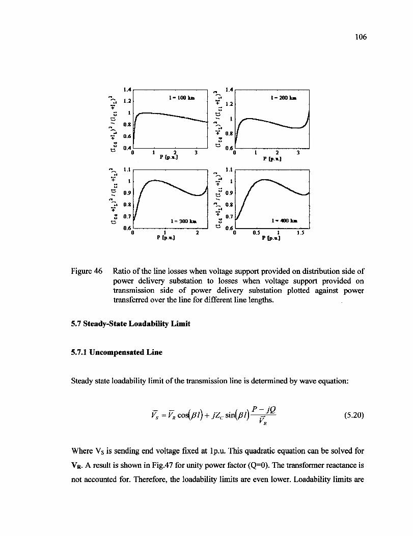
Reproduced with permission of the copyright owner. Further reproduction prohibited without permission.
106
1.4 ... 1.4 ~ ,.. 1 = 100 ba l=lOOka ~ 1.2 .. .. + 1.2 + -u
;:; ::::. ::::. -- 0.8
,.. ,. ~ .. ~ + .. 0.8 + 0.6 ... ... u
u 0.4 ~ 0.6 -..... 0 2 3 0 2 3 p (p.u.] p (p.u.]
,.. 1.1 1.1 ~ ... .. ...... + ..
1 ... + u ;:; - 0.9 0.9 - ::::. ,. -... 0.8 ... 0.8 ~
+ .. ... 0.7 + 0.7 u ... ::::. 1=300ka u -0.6 ~ 0.6
0 1 2 0 O . .S 1 u p [p.u.] p [p.u.]
Figure 46 Ratio of the line losses when voltage support provided on distribution side of power delivery substation to losses when voltage support provided on transmission side of power delivery substation plotted against pow~r transferred over the line for different line lengths.
5. 7 Steady-State Loadability Limit
5.7.1 Uncompensated Line
Steady state loadability limit of the transmission line is determined by wave equation:
- - J ) ( ) p- jQ Vs = VR co~f3/ + jZc sin f3/ -----=='-~ VR
(5.20)
Where Vs is sending end voltage fixed at lp.u. This quadratic equation can be solved for
Va. A result is shown in Fig.47 for unity power factor (Q=O). The transformer reactance is
not accounted for. Therefore, the loadability limits are even lower. Loadability limits are

Reproduced with permission of the copyright owner. Further reproduction prohibited without permission.
107
3.92, 2.03, 1.44 and 1.17 p.u for 100, 200, 300 and 400 km line lengths, respectively.
Surge impedance load PsiL = 1p.u.
1.4 ------r-----1------7------i------r------i------~------;
o : :Trans~ssion si!fe voha~e V R : o
1.2 ____ . _: _____ -~- ____ .l. ___ (n.!JP:~~!DJ!.~_a_l!:~-~e)- __ ] ______ ; 1 1 1 1 1 1 1 1 ...... 0
:s Cl. 1 1 1 1 1 1
v 1 c. 0
----- t------:---- .J -:- t 00-S.----- -1 • --0 > 0.8 A 0 .... • • 0.6
11! • a • 0.4 ... E-1 ....... ~ 0 0
> 0.2 -----·------~-----~------~------~ 0 0 0
0 0 0
0 0 1 1.5 2 2.5 3 3.5 4
p [pu]
Figure 47 P-V curves for non compensated line. Surge impedance load PsiL =1p.u. The effect ofthe transformer reactance Xris not considered.
5. 7.2 Compensated Line
5.7.2.1 Distributed SVS on Distribution Side ofSubstation
When distributed SVSs are sat on distribution si de of power de li very substation, as in Fig.
38 (Fig.44.a)), Qd required for distribution side voltage regulation VL is given by
equations (5.11) and (5.12). Fig. 48 shows reactive power Qd needed to regulate
distribution side voltage IVLI at l.p.u. plotted versus active power P transferred over the
line. The coefficient ll.Q/ ll.P (reactive power injected into the system needed to maintain
distribution voltage VL at 1p.u. for increase in power transferred over the line) is the

Reproduced with permission of the copyright owner. Further reproduction prohibited without permission.
108
measure of the system degradation. For theoretical loadability limit in steady state,
ll.Q/ ll.P tends to infinity. It marks the point beyond which voltage regulation by shunt
compensation becomes impossible (turning point on P-V curve). For practical application
it is suggested that ll.Q/ ll.P should not exceed 0.9. From Fig. 48 it can be seen that steady
state loadability limit is significantly increased compared to non-compensated line.
Before proceeding further, sorne explanations regarding Fig. 48 are required. The
transformer reactance changes with transformer rating. In our calculation we assumed
transformer impedance 10% on the transformer base. The maximum power delivered
across the transformer is its rating. Loadability oflines changes with line lengths. For 400
km line, transformer rating is assumed to be PMAX=SMAX = 1.5 p.u., for 300 km line PMAX
= SMAX = 2.5p.u., and for 200 km and 100 km line PMAX = SMAX = 3.5 p.u., where PsiL =
lp.u .. 3.5 PsiLis considered to be the thermallimit ofthe line (X-r= 0.1/M(p.u.) where M
= SMAX/ PsiL)·
5. 7 .2.2 Lumped SVSs on Transmission Side of Substation
When lumped SVS is situated on transmission side of power delivery substation as in
Fig.39 (Fig.44 b)), QI required for transmission voltage regulation with lumped SVS
(given by equations (5.8) and (5.9)) is plotted against active power transferred over the
line for different line lengths as shown in Fig.5.49. It can be seen that loadability of the
lines is further increased comparing to case when voltage regulation is provided on
distribution level, but not considerably. Moreover, the loading of200 km line and shorter,
is already extended to thermallimits with distribution, distributed SVS.

Reproduced with permission of the copyright owner. Further reproduction prohibited without permission.
3. 5 --------- -;-----_-- --- -;--- ------- ï- -- -- ----- ï--------- - i Reacbve po'ifer needed fee 1 1
distributioa side voltagt! V regulation : : 3 --------- -:--- ------- -!-- .J._ --- --- ~-- --- ---- ~--------- - ~
...... 2.5 ::s
' ' ----------~---------~----------~----
' ' ' ' a.
2 ----------:---- _1_=:;- JO~_Jpp_ ' 1
' ' ' ' ----------r-------
' 1 --------- _,__--- ---1
' ' '
' ' ' Ô 0.5 --~----------~----------~ 1 1 '
' 1 ' ' 1 1 1
1 1 ' 1 0 ~=~-.... ..-;.-~--------- -·---------- .,----------.,----------, -0_5~------~------~--------~------~------~
0 2 3 4 s p [pu)
109
Figure 48 Qd - P curves for line compensated with distributed SVS on distribution side of power delivery substation. Surge impedance load PsiL =lp.u. The effect of the transformer reactance is included.
4.S
4
..-.3.5 ::s a. ... v 3 Ir> g_ 2.5 v > 2
"D 0 • 1.5 v ... ..... - 1 Cl
0.5
0
: Reactive p~wer needed•for __ Jnoa~jÜDD..ullc_-v:~ac X._-~ati&ln. ___ _
1 1 '
: : t:= 200 km ----------~---------~----------~--------' ' ' '
' ----------L---------~----------~------- --~----------1 '
' ' ' '
--------- -:----- - - -1-:z-:300-, 1
' ' ----------r---------
' ' ' ' ____ ï __________ ï _________ _
' '
b~ ... ~!ll!!-~-~--~-~-_:-:-_- -:---------- ~------ ---- ~----------1
' -0.5~------~-------L--------~------~------_J 0 2 3
p [pu] 4 s
Figure 49 Ql - P curves for line compensated with lumped SVS on transmission side of power delivery substation. Surge impedance load PsiL =lp.u. The effect of the transformer reactance is included.

Reproduced with permission of the copyright owner. Further reproduction prohibited without permission.
110
5.8. Hypersim Digital Simulation
To demonstrate feasibility and reliability, a detailed numerical, real time simulation has
been performed. Hypersim was used for this study. HYPERSIM is based on EMTP
software mostly. The main advantage of HYPERSIM is availability of high precision
models of lines, loads and SV Cs based on experience of many years of R&D at IREQ.
Importance of real time dynamic simulation is in fact that long term dynamic stability
study can be performed to insure that there are no long term instabilities following
contingency situations.
5.8.1 Studied System
The studied system consists of315/25 kV, 200 km double circuit, radial transmission line
delivering power to three load centers (as in Fig.38 with K=2 and N=3) shown in Fig.50.
Line is transposed and each 50 km of the line is modeled with its TI nominal circuit. Load
is fed over three power transformers, each rated at 400 MV A. Loads of the test system
are modeled in detail. Each load is an aggregate of induction motor, static load available
as default model in Hypersim, and resistive load. The active and reactive powers
consumed by static load are fonctions of the voltage level and frequency according to
(5.21) and (5.22).
(5.21)
(5.22)

Reproduced with permission of the copyright owner. Further reproduction prohibited without permission.
111
Load power factor is mostly corrected with switched and fixed capacitors connected on
distribution buses. The principal parameters of test system are listed in the Appendix C.
Motor parameters are taken from [1]. Detailed model description is given in [72].
315 kV 1
l ~
1
f ( 1
25 kY ~us, '-a-/ fous, '-a-/ 1 11111 1 11111
( ({((( ( {((({ ~!U! ~U!
Figure 50 Test System
S.8.2 Lumped vs. Distributed Distribution SVS
1
{
• ~ {BUS ' 3
1 1 Ill
{ {{{{{ dJW!
First, voltage support is provided with lumped SVC consisting of three Thyristor
Switched Capacitors (TSC) circuits Y- connected and Thyristor-Controlled Reactor
(TCR) delta connected. Default model of SVC with complete control and measurement
system is available in Hypersim. Its detailed description is given in [72]. SVC is
connected on transmission side of substation on 315 kV bus via step up transformer. Each
TSC can supply 75 MV Ar for total of225 MV Ar. Each branch is tuned with series reactor

Reproduced with permission of the copyright owner. Further reproduction prohibited without permission.
112
to 5th harmonie. Additional filtering is provided with fixed capacitor tuned to 5th and 7th
hannonic. High pass filter is also added. Total power transferred over the line is 750 MW.
5.8.2.1 Loss of SVS
Fig. 51 shows the simulated waveforms of the power transferred over the lines,
transmission side voltage of substation seen by SVC measurement circuit, phase ab
current of one TCR and phase a currents of each TSC branch. The SVC is suddenly lost
at 0.1 ms. The loss of SVC is apparent in disappearance of its currents. It can be seen that
voltage drops instantaneously for about 20% and then continues to decay, leading to
complete voltage collapse. It is clear that additional unit is needed as stand by with its
own step up transformer to assure reliability. The same happens if SVC's transformer is
lost to fault.
The same test, under the same conditions of operation is performed when voltage support
is provided with three distributed, distribution SVC. Each load bus has its own SVC
providing voltage support. Each SVC consists of one TCR delta connected and three
branches of TSC Y-connected. Each SVC can provide total of 75 MV Ar. Fig.52. a), b),
and c) shows simulated waveforms for the loss of SVC3. From Fig. 52 it can be seen that
voltage on load buses do not drop more then 5% and recover after 100 ms. The SVC1 and
SVC2 respond to loss of SVC3 with switching on their third TSC branch to compensate
for the lost SVC3. This shows the superiority of distributed, distribution voltage support
sc herne.
5.8.2.2 Loss of the line
The most onerous system contingency is loss of one transmission circuit. Outage of one
line increases reactive and resistive voltage drop increasing reactive needs of system as it
can be seen from Table m. If system is not designed with enough reactive reserve, line

Reproduced with permission of the copyright owner. Further reproduction prohibited without permission.
113
tripping can lead towards complete voltage collapse. Fig. 53 shows response of lumped
SVC on transmission side of substation a:fter the line tripping at 0.1 sec. Immediately a:fter
the fault, SVC undervoltage protection disconnect SVC and system voltage collapses
instantaneously.
Fig. 54 shows response on same fault when voltage support is provided with three
distribution side SVC, each having 75 MV Ar capacity. Fig. 54 shows voltage seen by
SVC measurement circuit, TCR phase current and a phase currents of each TSC branch.
Each SVC responds immediate! y a:fter the fault turning off TCR and switching in ali TSC
branches. Total power transferred over the line before line tripping is 730 MW or 2.1 p.u.
After the line outage, this power is redirected over the remaining line. System is designed
to support 1.5 p.u power transfer over each line for a total of 1000 MW. Due to lack of
reactive power, voltage decays and stabilizes at about 0.65 p.u .. Reactive power provided
by SVC decreased as a square of the voltage, clearly indicating disadvantage of
impendence type compensators. They provide the least when they are most needed,
showing that nameplate rating of SV Cs has to be increased. After 1 sec. line is re-closed
and voltage recovers but never at 1 p.u. It is worth noting that even after the line re
closing and voltage recovery the post fault conditions are not equal to pre-fault conditions
as it can be seen from lowest trace of Fig. 54 a) toc). Each TSC branch of every SVC
stays on and TCRs are off. This is due to increase reactive power demand from
accelerating induction motors.
5.8.3 STATCOMvs SVC
The same system is simulated with the difference that ail three SVCs are replaced by three
lower rating STATCOMs. Each ST ATCOM consists of voltage controlled Voltage
Source Converter and its control circuit. The control circuit is described in detail in [63]
and is not available as default model in Hypersim.
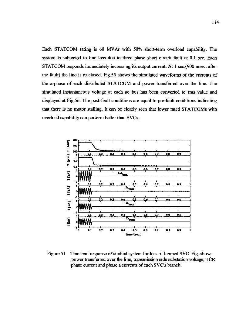
Reproduced with permission of the copyright owner. Further reproduction prohibited without permission.
114
Each STATCOM rating is 60 MV Ar with 50% short-term overload capability. The
system is subjected to line loss due to three phase short circuit fault at 0.1 sec. Each
STATCOM responds immediately increasing its output current. At 1 sec.(900 msec. after
the fault) the line is re-closed. Fig.55 shows the simulated waveforms of the currents of
the a-phase of each distributed STATCOM and power transferred over the line. The
simulated instantaneous voltage at each ac bus has been converted to rms value and
displayed at Fig.56. The post-fault conditions are equal to pre-fault conditions indicating
that there is no motor stalling. It can be clearly seen that lower rated STA TCOMs with
overload capability can perform better than SV Cs.
Figure 51 Transient response of studied system for loss of lumped SVC. Fig. shows power transferred over the line, transmission side substation voltage, TCR phase current and phase a currents of each SVC's branch.

Reproduced with permission of the copyright owner. Further reproduction prohibited without permission.
~ :F;:;; ~ : ~; : : : : l ~-~-0 ~ ~ u u u u v u u 1
~-:~-0 ~ ~ u u u u v u u 1
~"':--1000~.~~~~~--~~--~--~~--~--~----J---~----J
~
100000 0 .• 1 0-2 u 0.4 o.s 0.41 0.7 0.1 u 1
-1000~--~~~~--~~~----~--~----J---~----J---_J
0 0.1 0-2 0.3 0.4 o.s 0.41 0.7 0.1 0.9
ta.{..:.)
(a) SVCt dynamic response for the loss ofSVC3.
~ ];:;.: -~ : ~' : : : : l ~:~·-:--1oooL-.--~L.....:.--~--~~--J---~ ____ J-__ ---~. ____ J-__ ---L----'
~·-:~ ·10001-·----'~--~----'~--J---~----J---~----J------L----'
~J·:·~ 0 ~ ~ u u u u v u u 1
tÎIBe (MC.)
(b) SVC2 dynamic response for the loss of SVC3.
115

Reproduced with permission of the copyright owner. Further reproduction prohibited without permission.
~ ];:; .; : v~ : : : : l ~ JN( ~ ·~ ~· ~ ~ ~, ~· ~ i (~Mf ~ ~ ~· ~ ~ .,, ~· ·~ i ~ :~~r ~· ~ ·~ ~ ~· .,, ~ ~ 1
~ J ·:· ~ ~ ~· ~ ~ ~, ~ ·~ i 0 u ~ ~ - ~ ~ v u ~ 1
tiale [..:.]
(c) SVC3 dynamic response for the loss of SVC3.
Figure 52 Transient response of studied system for the loss of SVC
Figure 53 System transient response for one line tripping at 0.1 sec when voltage support provided with one lumped SVC on transmission side of substation.
116

Reproduced with permission of the copyright owner. Further reproduction prohibited without permission.
117
Figure 54 a) The SVC1 dynamic response. (Bus voltage, TCR phase current and phase current of each branch of TSC).
svc2
• 0.:~. VBUS2 l .!: :llo 0.4 0 1.5
..... ":1 1
~
-SOO
1000°
< - 0
-1000
1000
3: 0
-1000
1000
~ 0
-1000 0 o.s 1 1.5
tîmef..:.]
Figure 54 b) The SVC2 dynamic response. (Bus voltage, TCR phase current and phase current of each branch of TSC).

Reproduced with permission of the copyright owner. Further reproduction prohibited without permission.
118
svc3
7 0.:~ VBUS3 l ~ > 0.4
0 l.S soo
~
o.s tm. l-=-1
l.S
Figure 54 c) The SVC3 dynamic response. (Bus voltage, TCR phase current and phase current of each branch of TSC). Line is lost at 0.1 sec. and re-closed at 1 sec. when voltage support provided with three distribution SVCs.
3:~---.--~.------.--· --,.----r-: ~ --r----11
-3.5 ~...-_..___..L.-_~-~---L..--'---L---L----1---' 0 0.2 0.4 0.6 0.1 1 1.2 1.4 1.6 1.1 2
Figure 55 A system transient response when one transmission line lost at 0.1 sec. due to three phase fault. The fault is cleared and line is re-closed 900 msec. after the fault.
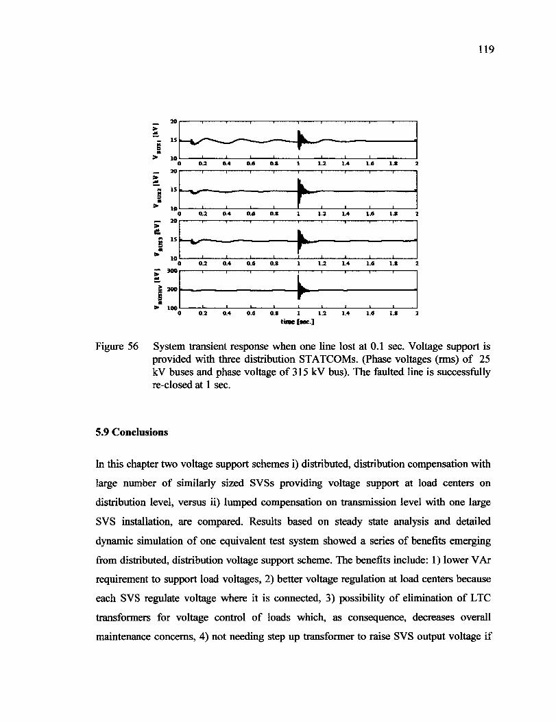
Reproduced with permission of the copyright owner. Further reproduction prohibited without permission.
119
Figure 56 System transient response when one line lost at 0.1 sec. Voltage support is provided with three distribution STATCOMs. (Phase voltages (rms) of 25 k V buses and phase voltage of 315 k V bus). The faulted line is successfully re-closed at 1 sec.
5.9 Conclusions
In this chapter two voltage support schemes i) distributed, distribution compensation with
large number of similarly sized SVSs providing voltage support at load centers on
distribution level, versus ii) lumped compensation on transmission level with one large
SVS installation, are compared. Results based on steady state analysis and detailed
dynamic simulation of one equivalent test system showed a series of benefits emerging
from distributed, distribution voltage support scheme. The benefits include: 1) lower V Ar
requirement to support load voltages, 2) better voltage regulation at load centers because
each SVS regulate voltage where it is connected, 3) possibility of elimination of LTC
transformers for voltage control of loads which, as consequence, decreases overall
maintenance concerns, 4) not needing step up transformer to raise SVS output voltage if

Reproduced with permission of the copyright owner. Further reproduction prohibited without permission.
120
SVS is installed on distribution level, 5) enhanced reliability, 6) lower standby
requirement in order to satisfy N-1 reliability criterion and 7) lower line losses.
However, for each line, depending on line length and loading, there is point beyond which
distribution si de compensation becomes inefficient in terms of V ARs needed for voltage
support and line losses. Although distribution side compensation increases transmission
capacity of the line, if further increase is needed, it can be obtained by transferring voltage
support on transmission level. Loadability of 200 km and shorter lines can be extended to
thermallimits with distribution side voltage support.
Detailed dynamic simulation of one test system has demonstrated feasibility and
advantages of proposed voltage support method. Moreover, it has been shown that lower
nameplate rating STATCOMs with short time overload capability can perform better then
impedance based compensator deviees.

Reproduced with permission of the copyright owner. Further reproduction prohibited without permission.
CHAPTER6
REACTIVE POWER REQUIREMNTS EV ALUATION-PHASOR APPROACH
6.1 Introduction
In this chapter, a step further is undertaken toward generalization of the proposed
concept. Two load centers, spaced along the transmission line are considered and two
proposed voltage support approaches are compared. In order to generalize the proposed
concept, general equations for reactive power requirement for voltage regulation are
deduced. The advantage of deduced equations over traditional power flow equations is in
lower number of itemtions because, for sorne cases, reactive requirement of compensator
can be deduced explicitly, not implicitly, as in classical power flow calculation.
Moreover, the proximity to voltage collapse can be monitored from deduced equations.
6.2 Reactive Power Requirement Calculation
In this section the equations that enable calculation of compensator mting and reactive
power needs of power systems are deduced. Tmnsformer reactances are also considered.
Objective is to deduce general equations applicable to geneml distribution of compensator
and meshed network.
6.2.1 One Load Center, Voltage Support Provided on Transmission Side of
Substation
Fig. 57 .a) illustmtes the case of one line feeding one load center over the transformer
having leakage reactance jXT. Fig.57.b) represents corresponding vector diagram showing
steady state solution for the circuit in Fig.57.a).
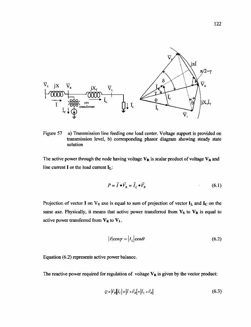
Reproduced with permission of the copyright owner. Further reproduction prohibited without permission.
122
rt/2-y
Vs J·x V R
---+ ---+ 1 - HV L
1 _ ;Y transformer
le+~
Figure 57 a) Transmission line feeding one load center. Voltage support is provided on transmission level, b) corresponding phasor diagram showing steady state solution
The active power through the node having voltage V a is scalar product of voltage V a and
line current 1 or the load current IL:
(6.1)
Projection of vector 1 on V R axe is equal to sum of projection of vector IL and le on the
same axe. Physically, it means that active power transferred from Vs to Va is equal to
active power transferred from V a to V L·
(6.2)
Equation ( 6.2) represents active power balance.
The reactive power required for regulation of voltage V a is given by the vector product:
(6.3)

Reproduced with permission of the copyright owner. Further reproduction prohibited without permission.
123
(6.4)
Equation (6.4) represents reactive power balance for circuit in Fig.57.a).
Projection of vector 1 on axe in quadrature with voltage V a plus projection of vector IL on
the same axe is equal to compensating current le.
From phasor in Fig. 57.b), it can be written:
( tr ) _ . _lvRI-Ivslcoso co\ 2 -y - smy- !XII (6.5)
(6.6)
(6.7)
(6.8)
(6.9)
combining (6.3),(6.7) and (6.9)gives reactive requirement for regulation ofVR.
Reproduced with permission of the copyright owner. Further reproduction prohibited without permission.
124
(6.10)
The equation (6.10)) can be obtained applying law of conservation of reactive power
through the node having the voltage V R· lt can be stated that total reactive power sent
from the node having the voltage V R is zero.
The reactive power sent from receiving end voltage V R to sending end voltage Vs is :
(6.11)
The reactive power send from receiving end voltage V R to load is:
(6.12)
and fmally, the reactive power send from node with voltage VR to compensator is:
(6.13)
Summing (6.11),(6.12) and (6.13) yields (6.10).
Voltage VL can be calculated using Pithagora's theorem as:
(6.14)

Reproduced with permission of the copyright owner. Further reproduction prohibited without permission.
125
(6.15)
and
(6.16)
(6.17)
Similarly, angle e can be calculated.
6.2.2 N Load Centers, Voltage Support Provided on Transmission Side of
Substation:
If we have N loads in parallel then reactive power needed for support of voltage V R is:
(6.18)
(6.19)
In case voltage VR is kept at 1 p.u, and voltage Vs is kept at 1 p.u., voltages VLi can be
expressed as function of VR using Pythagoras's theorem as in (6.15), angles 8i can be
expressed in terms of active powers as in (6.17) and compensating current le can be
deduced explicitly.

Reproduced with permission of the copyright owner. Further reproduction prohibited without permission.
6.2.3 Two Load Centers in Parallel with lndependent Voltage Support on
Distribution Side
126
Fig. 58.a) illustrates the case of two load centers having independent voltage support on
distribution level and Fig. 58.b) illustrates the phasor for the same circuit. To calculate
reactive requirements for distribution voltage regulation, first transmission voltage V a has
to be calculate. The receiving end voltage Vacan not be expressed explicitly.
Figure 58 a)Two load centers having voltage support on distribution level, b) corresponding phasor diagram.
The line current 1 can be decomposed into two components; one in quadrature with
voltage Va and the other in phase with voltage Va.
(6.20)
Equation (6.20) represents balance of reactive powers.
(6.21)

Reproduced with permission of the copyright owner. Further reproduction prohibited without permission.
127
Equation (6.21) represents balance of active powers. The y, Yt and Y2 are the angles the
currents I, It and h formed with voltage VR, respectively. For the sake of the clarity the
phasor ofFig.58 b) is decomposed into two parts as shown in Fig.59.a) and 59 b).
··-. ····- ...
(a) (b)
lv 1 ù IV 1 ! n/2-{ 1-·---·---·---·---·---·-
Ll COS 1- R i • v .---' JXnl1 LI
__ ......... --····-···· VR _______ ----· n/2 -y
1
(c)
Figure 59 a) First part of phasor from Fig 58.b) second part of phasor from Fig.58.b), c )zoomed part in circle from Fig.59 b)
From phasor diagram in Fig.59.a) it can be written:

Reproduced with permission of the copyright owner. Further reproduction prohibited without permission.
Il . lvRI-Ivslcost5
1 smy = X
From Fig.59.b) and 59.c) it can be written:
substituting in (6.20) yields (6.26)
Equation (6.26) can be obtained applying Kirchho:trs laws on circuit from Fig 58 a).
Applying Kirchho:trs laws on circuit from Fig. 58 a).
V8 =VR+ jXl
VR = jXrJI + VLI
VR = jXT2l2 + VL2
f=f]+l2
128
(6.22)
(6.23)
(6.24)
(6.25)
(6.26)
(6.27)
Reproduced with permission of the copyright owner. Further reproduction prohibited without permission.
Vs= VR + jX(Il + /2)
VR -VLI -----'-'--------'= = Jt
jXn
VR -VL2 -----'-'------'= = 12
JXT2
129
(6.28)
Sending end voltage Vs together with load (distribution voltages) Vu and V L2 are
regulated at 1 p.u. Voltage VR is taken as reference voltage, therefore, it can be written as:
IVsl = 1; lvLll = 1; ... jvL21 = 1;
angle(V8 ; Vn) = ô
angle(VR; VLI) = -~ angle(VR; VL2) = -~
Vn = lvnleJoo
Combining (6.28) and (6.29) yields (6.30)
Equation ( 6.30) can be written as ( 6.31)
(6.29)
(6.30)
- x x x x lvniO +-+-) = cosô+ jsinô+-(cos~- jsin~)+-(cos~- jsin~) (6.31) XTl XT2 XTI XT2
U sing only real parts of ( 6.31) gives:

Reproduced with permission of the copyright owner. Further reproduction prohibited without permission.
130
-1 1 1 1 1 1 jvRj(-+-+-) =-cos§ +-(cos~)+-(cosb;)
x XTI XT2 x XTI XT2 (6.32)
~~~ lvRI lvRI 1 1 1 -+-+----cos§ --cos~ ---cos~= 0 X Xn X1'2 X Xn X1'2
(6.33)
Equation (6.33) is the same as (6.26). The (6.26) can be interpreted as conservation of
reactive power for node with the voltage VR.
Where:
Q is reactive power from bus with voltage V R to bus with voltage Vs
Q1 is reactive power from bus with voltage VR to bus with voltage Vu
Q2 is reactive power from bus with voltage VR to bus with voltage Vu
Taking imaginary part from (6.31) yields:
_!_sin§ --1-(sin~)--1-(sinb;) X Xn XT2
~+Pz+P=O
which represents law of conservation of active power.
(6.34)
(6.35)

Reproduced with permission of the copyright owner. Further reproduction prohibited without permission.
131
6.2.4 N Load Centers in Parallel with lndependent Voltage Support on
Distribution Side
In more general case when N load centers are connected in paralle1 as in Fig.60, it can be
written:
the angles Ôi (i= 1 ,2 ... N) are 1oad angles and they can be expressed through the power
supplied to load centers.
Similarly, 1oad angles are:
substituting (6.39) into (6.36)
cos4 = jvLinvRj2
- P/ Xii lvullvRI
(6.37)
(6.38)
(6.39)
lvllvLX -!'z2 Xiz XrzlvRI + ... (6.40)
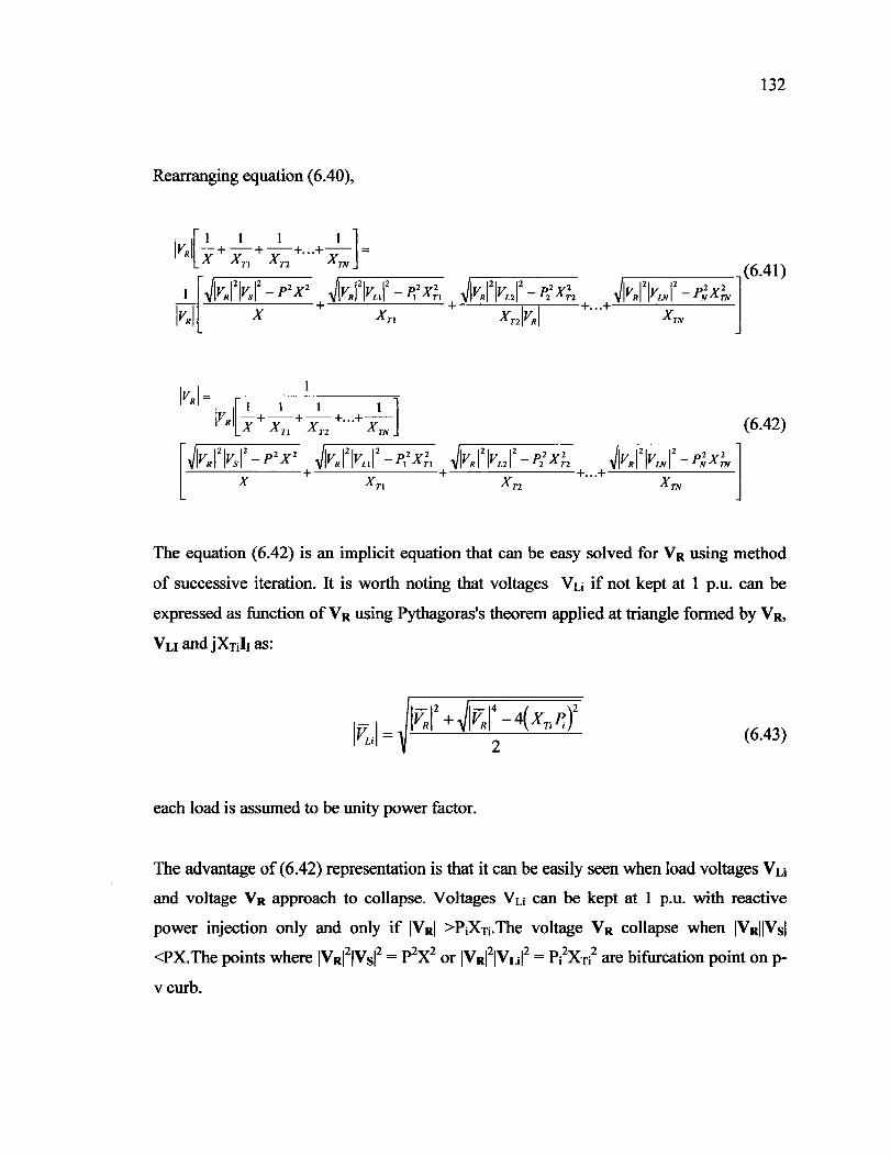
Reproduced with permission of the copyright owner. Further reproduction prohibited without permission.
132
Rearranging equation (6.40),
The equation (6.42) is an implicit equation that can be easy solved for VR using method
of successive iteration. lt is worth noting that voltages V Li if not kept at 1 p.u. can be
expressed as :function of V R using Pythagoras's theorem applied at triangle formed by V R,
Vu andjXTili as:
(6.43)
each load is assumed to be unity power factor.
The advantage of(6.42) representation is that it can be easily seen when load voltages Vu and voltage VR approach to collapse. Voltages Vu can be kept at 1 p.u. with reactive
power injection only and only if IVRI >PïXTi·The voltage VR collapse when IVRIIVsl <PX. The points where IVRI21Vsl2 = p2x2 or IVRI21Vul2 = P?XT? are bifurcation point on p
v curb.

Reproduced with permission of the copyright owner. Further reproduction prohibited without permission.
133
Knowing voltage V R and load voltages V Li using law of eosines, the currents Ii can be
calculated as:
II;i = jv;J +I~J -2l~ll~ilcos4 Xr;
(6.44)
and compensating currents Ici are:
(6.45)
Figure 60 N load centers with independent voltage support on distribution level
6.3 Radial Line Feeding Two Load Centers Distributed Along the Line
Considera radial transmission line of Fig.61 a) feeding two load centers over two bulk
power delivery substations. Load center # 1 is located on arbitrary position between two
ends of the line while load center #2 is fixed where the line terminates. Voltage support
can be provided on transmission level as shown on Fig.61 b) or on distribution level as
shown on Fig.61 c). To underline the essentials, the simplified models and the phasor

Reproduced with permission of the copyright owner. Further reproduction prohibited without permission.
134
representation are used in this study. Each segment of transmission line is represented by
lumped inductive reactance whose value depends on the line segment length. The
resistive !osses are neglected. The power delivery substation transfonners, whose leakage
reactances are jXTï, bridge transmission side voltages to the distribution side voltages.
The V Ar compensators are treated as continues source of reactive current. The loads are
assumed power factor corrected. It allows to consider only reactive requirements for
voltage support.
VR2
V LIT Joad 1 Joad 2
(a)
--+ î
load J Joad 2
(b) (c)
Figure 61 a) Radial transmission line feeding two load centers over two power delivery substations distributed along the. line. b) Voltage support can be provided on transmission level c ).or on distribution level
6.4 Feasibility
Before proceeding to make comparison, it is necessary to establish that voltage support by
distributed, distribution V Ar compensator of Fig. 61 c) is mathematically feasible for

Reproduced with permission of the copyright owner. Further reproduction prohibited without permission.
135
different position of load centers. The steady state solutions are presented in the fonn of
phasor diagrams. The transmission line between sending end voltage Vs and receiving
end voltage VRt is represented by lumped inductive reactance jX1 and transmission line
between receiving end voltage V RI and receiving end voltage V R2 is represented by
lumped reactive inductance jX2.
6.4.1 Steady State Solution for Distribution Voltage Support
The phasor diagram of Fig.62 presents the steady state solution for the distributed,
distribution side V Ar compensation ofFig.61 c).
Figure 62 Phasor diagram for circuit ofFig.61. c)
The sending end voltage Vs and load voltages Vu and V L2 are maintained on the circle of
the 1 p.u. voltage radius. The closing side of voltage triangle Vs, VR1 is the voltage phasor
jX11 where 1 is the current through the frrst segment of the transmission line. The sending
end voltage triangle satisfies Kirchhoffs voltage law: Vs= VR1 + jX11. It can be seen that
the transmission level, receiving end voltage VR1 is not regulated at 1 p.u. The receiving

Reproduced with permission of the copyright owner. Further reproduction prohibited without permission.
136
end voltage triangles satisfy Kirchhofl's voltage law: VRt =Vu+ jXn(Iu+ lct) and VRt
= V L2 + j(X2+ X n)(IL2+ la) where jX n lu represents voltage drop caused by load current
lu across frrst power delivery substation transformer, jXnlct represents voltage boost
due to leading current flowing through transformer reactance, V L2 is regulated voltage of
second substation and j(X2+ Xn)(IL2+ la) is voltage drop/boost across the second
segment of the line and power delivery substation transformer.
The Kirchhofl's current Law at the receiving ends 1 and 2 is: 1 = 12+ 11 where l2 = IL2 +
lc2 and lt = lu + let· It is apparent from Fig.62 that load voltages Vu and VL2 are
regulated while transmission voltages VRt and VR2 are not.
6.5 Reactive Requirement
6.5.1 Distribution Side Compensation at Buses Vu and VL2
The reactive requirements for regulation of load voltages Vu and V L2 can be calculated
from phasor diagram of Fig.62. using (6.42) The current through power delivery
substation #1, 11 can be calculated from eosine theorem applied on triangle formed by
load voltage Vu, receiving end voltage VRt and voltage drop jXn11 caused by the current
11 across substation # 1 transformer:
(6.46)
The compensating current Ic1 is in quadrature with load current lu(the load power factor
is assumed corrected). These two currents form right angle triangle together with current
11• Applying Pythagoras's theorem:
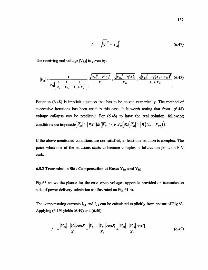
Reproduced with permission of the copyright owner. Further reproduction prohibited without permission.
137
(6.47)
The receiving end voltage IVR11 is given by,
Equation (6.48) is implicit equation that has to be solved numerically. The method of
successive iterations has been used in this case. It is worth noting that from (6.48)
voltage collapse can be predicted. For (6.48) to have the real solution, following
conditions are imposed:{IVR11 ~ IPX11)&(1vRII ~ I~Xnl)&(lvRII ~ I~(X2 + XrJ).
If the above mentioned conditions are not satisfied, at least one solution is complex. The
point when one of the solutions starts to become complex is bifurcation point on P-V
curb.
6.5.2 Transmission Side Compensation at Buses V Rt and V R2
Fig.63 shows the phasor for the case when voltage support is provided on transmission
side of power delivery substation as illustrated on Fig.61 b).
The compensating currents lc1 and lc2 can be calculated explicitly from phasor of Fig.63.
Applying (6.19) yields (6.49) and (6.50):
(6.49)

Reproduced with permission of the copyright owner. Further reproduction prohibited without permission.
138
(6.50)
where IVRti=IVR21=1Vsl=l p.u.
and Vu and Vu are load voltages that can be calculated using Pythagoras's theorem as:
lvRJ = lx rJ LJ + lvLJ and knowing that l'; = lv Li III Li 1 , i= 1 ,2.
(6.51)
Figure 63 Phasor for transmission side voltage support
6.6 Comparison of Two Voltage Support Schema
6.6.1 Comparison of Var Requirement
Reactive power needed for voltage support depends on power transfer over the line, line
length and position of load centers. Considering again the simple case of Fig.61 where
radial transmission line feeds two load center. Let real power supplied to load center #1 is
2 p.u and to load center #2 is 1 p.u. Assume line length of225 km. Surge impedance load

Reproduced with permission of the copyright owner. Further reproduction prohibited without permission.
139
is used as 1 p.u. Line is assumed lossless. Line reactance is 0.00131 where lis line length
in km. Transformer impedance is assumed 10% on transformer base. Load voltages Vu
and VL2 are regulated at 1 p.u. Load center #2 is situated at the end of the line, 225 km
from sen ding end. Load center # 1 is shi fied from sen ding end toward load center #2 (from
0 km to 225 km). Fig. 64 shows receiving voltages VRt and VR2 (upper trace), power
angles (middle trace) (ù is angle between Vs and VRt, Ùt is angle between VRt and Vu
and Ô2 is angle between V Rt and V L2) and reactive power Q 1 and Q2 (lowest trace)
needed to keep load voltages Vu and VL2 at 1 p.u., respectively, plotted against position
of load center # 1.
The Fig.65 compares reactive requirements for the same system when voltage support is
provide on transmission level keeping voltages V Rt and V R2 at 1 pu. It can be seen that
most of the time reactive requirement needed for distribution, distributed voltage support
are lower compared to transmission side voltage support.
6.6.2 Comparison of Transformer MV A Requirements
The Fig.66 shows MV A requirements of transformers for both cases plotted against line
length. When voltage support is provided at transmission level as in Fig.61 b)
transformers MV A requirements are evaluated as:
(6.52)
When voltage support provided on distribution level as in Fig.6.5.c) transformer MV A
are evaluated as in:
(6.53)

Reproduced with permission of the copyright owner. Further reproduction prohibited without permission.
Figure 64
Figure 65
~ ., 011 • ..!! 0
>
140
[~~~~~~~~~~~~~~~~~~;;~~;;~~~;t~~~ 1 1 1 1
0.9S - - - - - ~ - - - - - ~ - - - - - ~ - - - - - ~ - - - - - t ---nt
1
0.9~--~--~~--~--~----~--~----~--~--__J 0 100 12.5 uo 200
100.----.----.---~----~---,----.----,,----r---,
3.----.---.,---.----.----.---~----.----r----, 1 1 1 1 1 'Q 1 1
l -----~~----~-----~-----~-----~-----~--~-----~~ 1 1 1 1 1 1 --~_______........
0~-~-~-~-~-~~~-~-§-§-§-~~~-~-~-~-~-~~~-~-~-~-~-~:~~~:~~~·~~Q~Ï~t~~-~~-~-~~~-2~~,-~-~-:J-0 15 SO 1S 100 12S ISO 200 l2S
position of Joad center #1 [km)
Power delivery substation transmission side voltages (upper trace), power angles (middle trace) and reactive power (Q = Q 1 +Q2) needed for voltages regulation (lower trace) on distribution side.
2
u ~
:i ~ CY o.s
2 . .5.---.----,----,---~----.----r----.----.---.
O.S
-·v--~-----~-----~-----• 1 1 1 1 1 1 1
1 1 1 1 1 ---,-----,-----,-----r-----r-----r-----ï-----! 1
: Qdistfibwted : : : 0~--~--~----~--~----~--~----~---L--~
0 15 SO 1S lOO 12S ISO 11S 200 l2S position of Joad center #1 [km)
Comparison of reactive needs at substation # 1 and #2 plotted against position of load center # 1

Reproduced with permission of the copyright owner. Further reproduction prohibited without permission.
MV A of traasfOIIDCI" 4.8 ,---,---,---,---,---r---r--r--r--r----,
4.6 ------ --- .. - -.--.--:-. -----~ ·--.-. i --- ·-- i------ -:-------:------.
. . 42 ------ ... ----- .... -----:----- ... -~ --- .... - ~ ...... ---~-- ...... ~--- ....... -~ -- ----~- -- ......
~~ : : ~ ~ ~ 4 ------ ------ -------:-------:--- --f------i-------:-------:-------t-----
1 • ' 1 1 ' • • 1 1 • 1
1 ' 1 ' ' 1 1 1 • • • 1
3 .. 1 ----- ... ------ .. .. --:------ -~ -- ...... - -;- ----- ~--- .. --~- ----- -~ ...... --- -~-----. . . . . . . 1 1 1 1 1 1 1 1 1 1 • •
' ' • 1 1 1 1
---·------~------~------~------·------~------~-------~------~-----1 1 • 1 1 1 • 1 1
1 ' 1 1 • 1 • 1 ' ' 1 • 1 • • • • 1 • 1 1 • 1 • 1 1 1
1 1 1 1 1 1 1 1 1
----- i ..... - ... - -1- ........ - .. -:---- .... -:· .... ---- i .......... - .. i-- ... --- -:-- ...... - ... -:------- ~ ---1 ' ' 1 1 • 1 1 1 1 1 1 1 1 1
: : : :Sdisb~ed : 3...2 ----"' ... , ...... -- .. , ................. , .... - -- --r·-- -- '"T -- ........... , ... -
3 b:h::::::!::::±::J::I_j_j_j__j_J 0 ~ ~ ~ ~ ~ ~ ~ ~ ~ ~
line leagth (ba]
Figure 66 Transformer MV A requirements.
6.6.3 Transmission Level Voltage
141
In this subsection the case of two load centers, similar as shown in Fig.61 is considered.
The first 1oad center is located at line at 150th km from stiff system and the second 1oad
center is located 100 km further. Thermallimits of the 1ine are assumed to be 3Psi1 so 3pu
is used as P max·
Fig. 67 shows variation oftransmission level voltage VR1 (voltage on HV side of power
delivery substation 1 plotted against power transferred to load center #2. The power fed to
1oad center # 1 is fixed.
6.6.4 Comparison of Var Requirement
Fig.68 displays reactive requirement for two methods. The power fed to 1oad center #2 is
kept constant at 1 p.u. while power transferred to load center #1 is varied from 0 to 2 p.u.

Reproduced with permission of the copyright owner. Further reproduction prohibited without permission.
142
Upper trace in Fig.68 shows reactive requirements for load centers #1 and #2 when
voltage support is provided on transmission level. Lower trace shows reactive
requirements for load centers #1 and #2 when voltage support is provided on distribution
lev el.
1 ------;------~-------~------~------;------~------~-------~------~------~ • 1 1 1 • 1 • • 1
1 1 1 1 1 1 1 1 1
0 1 1 1 ' 1 1 • 1 ' 1 1 1 l 1 1 1
0.99 ------1 --- -i---- ---:-------:--- ........... t-- ........ i- .. - .. - ..... ; .. ------:- ... ---- -;.- -----1 1 1 1 1 1 1 1 1 1 1 1 • • 1 1 1
1 1 1 1 1 1
1 ' 1 1 1 1 , 1 1
. . . : Pl = 2 P-~ : : : : : : :
0.95 ------:----~~.fn-..Qo~l.P.!'--····~···· ~--·· ·+······~······~ 1 1 1 1 1 1 1 1 1 • ' • 1 1
1 1 1 1 1 1 1 ' 1
0.94 · · • · · · i- · · · · · ~ · · ·- · · -:- · · · · · .;pt..-I{S p.a- ~- ·- ·-. ~- ..... -:--- . - ~ ....•. ~ : : : :Pl~~Oto l~Sp.u.: : : ' 1 1 1 • 1 1 1 1 1
0.93 ------ t------ ;---- ---:-------:-------1------1-------:-------:------- r- ----.; • • • • • • 1 • • • 1 1 1 1 1 1 1 1 1 1 ' 1 1 1 1 1 1 • 1 1
1 1 1 1 1 1 1 1 1 '
0.910 0.4
Figure 67 Variation of transmission voltage V RI plotted against power P2 fed to load center #2. Ptmax +Pzmax = 3pu which is assumed to be thermal limit of the line.
It is worth noting that the saving in terms of$ can be considerable. Total Q for bulk case
is 1.42 p.u and for distributed is 1.33. So the difference is 0.09 p.u. The savings depends
upon the voltage level. In the case of 500 kV transmission line 1 p.u = 1000 MW. So the
savings in MV Ars are 90 MV Ar. If the STATCOM is 50$/kV Ar then savings are $4.5M.
Fig. 69 compares reactive needs for the case 150 km line feeding 2 p.u. load plus 100 km
line feeding 1 p.u. load when compensation is provided on HV side vs. compensation on
distribution voltage side. When compensation is on HV we keep VRI and VR2 at 1p.u,
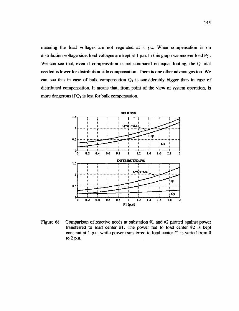
Reproduced with permission of the copyright owner. Further reproduction prohibited without permission.
143
meaning the load voltages are not regulated at 1 pu. When compensation is on
distribution voltage side, load voltages are kept at 1 p.u. In this graph we recover load P2.
We can see that, even if compensation is not compared on equal footing, the Q total
needed is lower for distribution side compensation. There is one other advantages too. We
can see that in case of bulk compensation Q1 is considerably bigger than in case of
distributed compensation. It means that, from point of the view of system operation, is
more dangerous if QI is lost for bulk compensation.
BUI.KSVS
1 1..2 1.4 1.6 u l
DIS'llUBUlED SVS LS.---.--~.---.---.---.--.---.--.--,----,
: : : : : Qooq1+Ql : : 1 w ~·- --;--- --- ~------ -:------ -~---- --;- ----- ~-- ----~-- :
• 1 • 1 • • t 1 1 1 1 1 1
1 1 ' 1 1 • 1 ' . . .
1 1..2 1.4 1.6 1.1 l
Pl (p.u]
Figure 68 Comparison of reactive needs at substation # 1 and #2 plotted against power transferred to load center #1. The power fed to load center #2 is kept constant at 1 p.u. while power transferred to load center #1 is varied from 0 to 2 p.u.

Reproduced with permission of the copyright owner. Further reproduction prohibited without permission.
144
BULKSYS
: l Q-Qt?-<P -+-----7--0a.-~ 1 ......................... -------:------·:--------·----.
lQt o_s ---- ... ! ............ -~--· ---7 .......... · -~ ·- ·- --~-- .. -· -~-·--- -~--·---·~--· -- -~-----
• 1 1 1 1 1 • 1
• ' 1 ' 1 1 1
oL-_L; --~; --~;-=~;==~;~~;~==~~:==~:==~:t:~ 0 0.1 0.2 0..3 0.4 O.S 0.6 0.7 0.1 0.9 1
DISllUBliTED SYS
b==~==;;;;~~:t~~·~~· ~~~. Os • . .
~------~-------~------·------4·-----~-------~-·----~-----. . . . . . . . 1 1 1 1 1 1 1 1 • • 1 ' • 1 1 1 1 1 1 . . .
o~--~--~--~--~--~--~--~--~--~~ 0 0.1 0.2 0..3 0.4 O.S 0.6 0.7 0.1 0.9 1
Pl [p.o]
Figure 69 Comparison of reactive needs at substation #1 and #2 plotted against power transferred to load center # 1. Comparison of reactive needs at substation # 1 and #2 plotted against power transferred to load center # 1. The power fed to load center #1 is kept constant at 1 p.u. while power transferred to load center #2 is varied from 0 to 1 p.u.
6. 7 Conclusion
In this chapter two load centers spaced along radial transmission line has been considered.
The equation allowing calculation of voltages and compensating currents for voltages
regulation have been deduced and veri:fied. Two methods for voltage support, namely,
voltage support of transmission line with distribution level compensation and voltage
support of transmission line with transmission level compensation, have been compared.
It has been shown that distribution level voltage support has signi:ficant benefits over the
transmission level voltage support. The bene:fits include lower var requirement, direct
voltage regulation of distribution buses and elimination of step up transformer for voltage
support.

Reproduced with permission of the copyright owner. Further reproduction prohibited without permission.
CHAPTER7
VOLTAGE SUPPORT OF LONG RADIAL TRANSMISSION LINES BY V AR
COMPENSATION AT DISTRIBUTION BUSES
7.1 Introduction
The objective of this chapter is to bridge the gap between transmission and distribution
approaches to voltage support and reactive power management. The impetus, which
should bring transmission system engineers and distribution system engineers together, is
the availability in the market of SV Cs which can be connected directly to the distribution
buses at voltages as high as 35 kV without step-up voltage transformers [68]. As it
requires concrete examples to demonstrate how the innovative advance can be exploited,
this chapter reviews where the potential benefits are and proceeds to substantiate the
daims in a case study of a 400 km long, 230 kV radialline supplying 200 MW to each of
4 loads spaced evenly along its length.
The case study is pattemed after Hydro-Quebec's 1000 km long James Bay line whose
voltage profile is supported by a combination of capacitors and static var compensators at
5 intermediate points along the line. If the intermediate points are not in the Canadian
wildemess but are in inhabited areas, the same concept can be applied to increase the
transmissibility of real power to distant townships at intermediate points spread along the
long line. As such a project falls within development and planning of transmission
systems, the capacitors and static var compensators (SVC) will be installed on the
transmission line buses.
One objective of this chapter is to highlight the advantages of distribution bus voltage
support to transmission system engineers who are charged with the development and
planning for the voltage support of long lines. In today' s restructured electric utilities, the

Reproduced with permission of the copyright owner. Further reproduction prohibited without permission.
146
many distribution systems and the transmission system may belong to different owners.
The technical and economie advantages can still be implemented by putting voltage
support as an ancillary service. The distribution system closest to the generation source is
providing capacitive reactive power not only for its own load but also for the loads of
distribution systems further down the line.
It is required to show that the concept is technically feasible. This is accomplished by
digital simulations. The simulation tool in use has been HYPERSIM. The successful
simulation firstly implies feasibility, meaning that there is a mathematical solution of the
operating point. Secondly, the operating point is steady-state stable, because otherwise
there is no stable convergence in the simulations. Finally, simulations have been used to
demonstrate that after three-phase-to-ground faults, the transmission line automatically
recovers its regulated distribution bus voltages.
In quantifying capacitive reactive power, this chapter makes a distinction between the
amount required for power factor correction and the amount required for voltage support.
In order to simplify bookkeeping, the amount required for power factor correction is
deducted in the accounting, so that one has a realistic value of the capacitive reactive
power required for voltage support. In this chapter, to provide voltage support (VS) by var
compensation, the authors use Static V ar Compensators(SVC) because it is proven,
mature and reliable technology.
7.2 Voltage Support of Long Transmission Line
Two transmission line voltage support schemes are presented in this section: voltage
support (VS) provided by SVCs on the transmission buses and VS provided by SVCs on
the distribution buses. Circle phasor diagrams are given to draw attention to the fact that,
unlike distribution system engineers who are concemed only with voltage support for the

Reproduced with permission of the copyright owner. Further reproduction prohibited without permission.
147
loads connected to the substation, transmission system engineers have to be concemed
with ali the loads along the transmission line.
7.2.1 Voltage Support at Transmission Buses
Fig. 70 shows a radial transmission line made up of M sections, each of which is
represented by an inductive reactancejXi, i=1,2,. M The generation source voltage is Vs.
At the ;th node, between two transmission line sections, the voltage is VRi. SVC providing
VS would be connected at each node to regulate the nodal transmission line voltage IV .J at 1.0 pu. Because the technology of the reactive power compensation is realized at the
level of distribution voltage, each installed SVC requires a step-up transformer to raise its
output voltage to the transmission voltage level ofVRi. The distribution bus (voltage V Li)
of the lh load center is coupled to the transmission bus (voltage V Ri) by a voltage step
down transformer which is represented by its leak:age reactance jXTi·
Fig.71 is a phasor diagram for the ith node ofFig.70. The phasor diagram is intended as a
pictorial representation of the steady-state performance of this system providing an
illustration of what is happening at a glanee. From Fig.71 it can be seen that, when the
transmission voltages are regulated, the tips of the per-unitized transmission voltage
phasors VRi, i=l,2 .. M, lie on a circle ofunit radius. The voltages oftwo adjacent nodes,
V Ri and VR(i-t), form two sides of a voltage triangle in accordance to Kirchhoff's Voltage
Law VR(i-t)=VRi+jXili where Ii is the line current through jXi, which represents the
reactance of the ith transmission line section. The voltage phasor jXili is perpendicular to
the current phasor li. Because of the voltage drop across the transformer leak:age reactance
jXTi by the load current ILi, the load voltage VLi =VRi - jXTiiLi is not regulated.
Transformer tap changers must be employed to achieve close load voltage regulation at
every node. As will be seen in Section 7 .5, transformer tap changers will not be needed
when the SVC regulates V Li, the distribution (load) bus voltage directly.

Reproduced with permission of the copyright owner. Further reproduction prohibited without permission.
148
From Kirchhoff's Current Law at the ith node, the capacitive compensating current is:
ICi=Ii-Ii+I-ILi. The compensating current Ici in Fig. 71leads the transmission bus voltage
VRi by 90°. The transmission bus voltages Va(i-I) and VRi lie on the unit circle. It is
assumed that lagging power factor in the load has already been corrected and therefore,
the load current ILi is in phase with VLi. The line current Ii is the vector sum of the load
current lu, the current through i+lth segment ofthe line Ii+I and the compensating current
Ici·
Figure 70 Single line diagram of radial transmission line feeding M load centers. Voltage support (VS) is provided on transmission buses.
Figure 71 Phasor diagram for ith node of Fig.70

Reproduced with permission of the copyright owner. Further reproduction prohibited without permission.
149
7.2.2 Voltage Support at Distribution Buses
This chapter advocates connecting the SVC providing VS to the distribution buses as
shown in Fig. 72. At the ith node, SVSï is set to regulate the load voltage at 1 Vu 1 =1.0 pu.
Fig. 73 shows the distribution bus voltages, Vu and VL(i-t), of the ith and (i-l)th nodes
lying on the unit circle under SVC regulation. SVCï, in providing voltage support to Vu,
supports the transmission bus voltage VRi also. The compensating current of SVCï. Ieï.
leads the distribution voltage V Li by 90°. The magnitude of the transmission bus voltage,
given by the formula, 1 vJ =1 Vu+jXTi(lu+jlci)l, is no longer at 1.0 pu. The current Iï+I
further down the line joins the transmission bus to form a second node at which the
current Ii=li+t+lu+lci· The transmission bus voltages form a voltage triangle in
accordance to Kirchhoff's Voltage Law VR(i-t)=VRi+jXïli.
Unlike distribution system engmeers who are responsible for the load current lu,
transmission system engineers have to look after the current Iï+t from further down the
line also.
Vs VRI VR(i-1) V Ri VRM
~
c ~~M
- ~""'' ~,, v"~ VL(•-1) ~- VLi - v,.~ IC(i-1) le; leM
svc 1 ~ svc(i-· -~ î ~ SVCM L(i-1)
IL; =- LM
Figure 72
=
Single line diagram of radial transmission line feeding M load centers. Voltage support (VS) is provided on distribution buses

Reproduced with permission of the copyright owner. Further reproduction prohibited without permission.
150
Figure 73 Phasor diagram for ith node of system using distribution bus VS
7.3 Comparison of Two Voltage Support Scbemes
7.3.1 Transformer Savings
At each node in Fig. 70, there is one transformer for the load and another transformer for
the SVC. Both the load and the SVC operate at low voltages and the objective of this
chapter is to point out that there is no reason to step-up the capacitive reactive power of
the SVC by one transformer to transmission voltage level and then to step it down again
to the distribution voltage of the load. By connecting the SVC directly at the load bus as
shown in Fig. 72, the SVC transformer can be saved.
7.3.2 Providin& (N-1) Reliability
There is further saving to be gained in the planning for (N-1) reliability. (N-1) reliability

Reproduced with permission of the copyright owner. Further reproduction prohibited without permission.
151
consideration requires that the voltage support be realized by N (t: 1) units. Should any
voltage support unit fail, the remaining (N-1) units must have sufficient Mvar capacity.
The cost of (N-1) reliability diminishes as N increases.
7.3.2.1 Distribution Buses Voltage Support
When Qm is the total reactive power required to provide voltage support of the ith node,
(N-1) reliability requires the reactive power to be divided into Nm smaller units. Upon
failure of any one unit, the remaining (Nm-1) units still provide the amount Qin· The (N-1)
reliability requirement of reactive power is therefore NmQin/(Nm-1).
Such division fits naturally in the design of distribution substations. such as shown in
Fig.32. The substation consists of: high-voltage line terminations, high-voltage busbars,
power transformers, low-voltage busbars and low-voltage line terminations. Breaker-and
a-half is used for both transmission and distribution voltage levels in order to fulfill the
reliability of power supply.
In the example of Fig. 32, when the real power requirement is Pï. (N-1) reliability is
satisfied by over-sizing each transformer to carry P/{NiD-1) watts (Nin=4 in the examp1e ).
In this situation, it is normal to allocate one SVC unit to each of the 25 kV buses. As the
transformers carry the real and the reactive powers, their total MV A requirement is
Nm(P?+Qm 2 )0
·5 /(NiD-1 ). As Nin increases, their total MV A approaches (Pi2+QiD 2 )
0·5
•
Furthermore, because (P?+Qm2)0
.5< 1 Pi 1 + 1 Qm 1, when the ratio Qin/ Pi is small, the
rating of the step-down transformers is only slightly increased by the need to carry
capacitive reactive power.

Reproduced with permission of the copyright owner. Further reproduction prohibited without permission.
152
7 .3.2.2 Transmission Buses Voltage Support
Using the same principle of dividing the reactive power QiHV required by the transmission
bus SVC into NiHV units, the total rating required to satisfy the (N-1) reliability criterion
is: NilwQiHV/(NïHV-1) for: (i) the reactive power and (ii) the step-up transformers. On the
load-side, the total MV A of the step-down transformers is NiDPi /(NiD-1 ).
7.3.2.3 Potential Reduction in Cost
In summary, the comparison of the two schemes are:
Reactive Power Requirements:
Distribution Bus SVC: NiDQii:Y'(Nïo-1)
Transmission Bus SVC: NiHVQiHV/(NiHV-1)
Transfonners MV A Requirements:
Distribution Bus SVC: NiD (P?+QiD 2 ) o.s /(NiD-1)
Transmission Bus SVC: NiDP/(NiD-1 )+NiHvQiHV/(NiHV-1)
As will be seen in the next section, QiD< QiHV· Furthermore, usually NiHv<Nio in
engineering practice. Therefore, the equipment requirement is less for SVC on the
distribution bus side than on the transmission bus side.
7.3.3 Reactive Power Savings
In general, QiD<QiHV, that is the reactive power required to provide voltage support is less
when the SVCs are located at the distribution buses than at the transmission buses.
However, there is a transmission length and a load limit beyond at which the inequality is
reversed, i.e. QiHV<QiD. This transmission length is near to where voltage collapse occurs.

Reproduced with permission of the copyright owner. Further reproduction prohibited without permission.
153
Approaching the problem by analysis, the point is close to the region where the solutions
are complex and therefore infeasible. In such a case, VS by shunt compensation alone is
not viable either on the transmission or the distribution buses. In such a situation, one
should consider increasing the transmission voltage or using a combination of series and
shunt compensation.
7 .3.4 Line Losses
The transmission bus voltages VR(i-I) and V Ri in Fig.72 are lower than those in Fig.70. For
the same real power transferred, the current Ii must be higher in VS on the distribution
bus than on the transmission bus and consequently this applies to the line losses. But as
will be seen in the case study below, the increase in losses is not substantial.
7 .3.5 Benefits
To summarize, the benefits of voltage support on distribution buses by var compensation
are:
i) lower transformer MV A requirements,
ii) lower var requirement for voltage support,
iii) close voltage regulation of the loads,
iv) lower oost in assuring N-1 reliability.
7.4 Proofs of Viability of Concept
The benefits will come to naught, if the system of Fig. 72 is not technically viable in the
first place. This chapter presents evidences on viability in a case study based on: (i)
existence of steady-state solutions; (ii) stability of steady-state solutions; (iii) ability of the
system to survive faults.
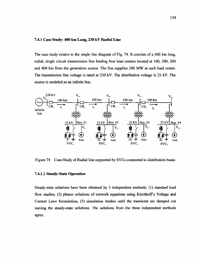
Reproduced with permission of the copyright owner. Further reproduction prohibited without permission.
154
7.4.1 Case Study: 400 km Long, 230 kV Radial Line
The case study relates to the single line diagram of Fig. 74. It consists of a 400 km long,
radial, single circuit transmission line feeding four load centers located at 100, 200, 300
and 400 km from the generation source. The line supplies 200 MW at each load center.
The transmission line voltage is rated at 230 kV. The distribution voltage is 25 kV. The
source is modeled as an infinite bus.
infinite bus
100km 100km
-----+ 1,
svc,
VRJ v R4
100 km 100 km -----+
I,
svc,
Figure 74 Case-Study ofRadialline supported by SVCs connected to distribution buses
7.4.1.1 Steady-State Operation
Steady-state solutions have been obtained by 3 independent methods: (1) standard load
flow studies; (2) phasor solutions of network equations using Kirchhoff's Voltage and
Current Laws formulation; (3) simulation studies until the transients are damped out
leaving the steady-state solutions. The solutions from the three independent methods
agree.

Reproduced with permission of the copyright owner. Further reproduction prohibited without permission.
155
The voltage phasors of V Ri and Vu are plotted in Fig. 75 The distribution voltage phasors
Vu, i=1,2 . .4, lie on the unit circle, whereas the magnitudes of transmission bus phasors
VRt to VR4 are 0.91, 0.92, 0.96 and 0.98 pu respectively. The large angle on the sending
end side and the crowding at the end reflect the fact that the line sections of currents 11, 12,
l3 and ~ in Fig.6 carry powers of 800 MW, 600 MW, 400 MW and 200 MW,
respectively.
1p:U.
VL4
Figure 75 Steady-State Voltage Phasors
7.4.1.2 Comparisons ofTwo VS Schemes
The 2°d and 4th columns of Table V summarize the reactive powers Qm of the SV Cs and
the complex powers 1 Sm 1 of the transformers at each node when VS is provided on the
distribution buses. The quantities are per unitized to the surge impedance loading of the
230 kV line (PsiL=211 MW).
The total requirements in Mvar and MV A are listed in the last row. For comparison, the
reactive powers Qmv and the complex powers 1 Smv 1 of the transformers for SVCs on the
transmission buses are listed in the 3rd and 5th columns. From the bottom row, one sees
the savings coming from the step-up transformers in the first 3 nodes. The reduction of Q

Reproduced with permission of the copyright owner. Further reproduction prohibited without permission.
156
(603-494) Mvar looks small but in terms of dollars capacitive Mvar is more costly than
transformer MV A. The numbers in Table V do not include the requirements of (N-1)
reliability.
Table V
High Voltage Bus vs Distribution bus for the test system from Fig.74
node QiD Qmv lsiDI 1 Smvl 1 reactive reactive trans for trans for
power power mer mer
1 0.904 pu 1.515 pu 1.311 pu 2.465 pu
2 0.756 pu 0.818 pu 1.214 pu 1.768 pu
3 0.429 pu 0.529 pu 1.042 pu 1.479 pu
4 0.251 pu NIL 0.983 pu 0.95 pu
L 2.341 pu 2.862 pu 4.549 6.662 pu
L 494 Mvar 603 Mvar 959 1405 MVA MVA
7.4.1.3 Comparison of Transmission Line Losses
As 1 V Ri 1 < 1.0 for every node in Fig. 75, it is expected that the current Ii in every
transmission line section is higher than for the case of transmission bus VS which
regulates the node voltage at VRi=l.O. As transmission line power loss is proportional to
1 Ii 12, the power loss is expected to be higher for distribution bus VS than transmission
bus VS. Fig. 76 plots the ratio of total transmission power loss (distribution bus
VS)I(transmission bus VS) as a function of the real power loading at every bus.

Reproduced with permission of the copyright owner. Further reproduction prohibited without permission.
157
1.16
1.14
1.12
1.1
0 ".D
1.08 • ~ -- 1.06 0 ...:1
1.04
1.02
50 100 150 200
Rcu Power of i-th Node [MW)
Figure 76 Ratio (distribution bus VS)/(transmission bus VS) of Transmission Line Losses
Up to 100 MW, the difference is negligible. At the peak loading of200 MW, the increase
is only around 16%. From the cost viewpoint, it is the difference in energy loss (time
integral of power) which is significant. The peak load occurs only for a small fraction of
the time.
7.4.1.4 Comparison of the Cost
The comparison of cost is shown in Table VI. The 2nd and 5th columns list the inductive
Mvar/ capacitive Mvar requirements of the 4 nodes for distribution and transmission bus
compensation respectively. The cost of thyristor switching is estimated as $40/k.V AR on
the distribution level and 50 $/k. V AR at transmission level. The difference in the cost is
due to the transformer that is assumed to be 20% of equipment cost [19]. Thus, the entry
for node 1 under Qm SVC is $10.5million=$40x(65+195)x103. For comparison the same
cost for high voltage bus compensation under QiHV is $22m.

Reproduced with permission of the copyright owner. Further reproduction prohibited without permission.
158
Table VI
Cost Estimate (SVC consisting ofTCR -TSC)
node Qm Qm Qmv Qmv
1 [Mvar] [$million] [Mvar] [$million]
svc N-1 svc N-1
1 -65/+195 10.5 3.5 -110/+330 22 22
2 -55/+160 8.6 2.87 -60/+180 12 12
3 -30/+90 4.8 1.6 -40/+120 8 8
4 -20/+60 3.2 1.1 NIL NIL NIL
L -170 27 9 -210 42 42
+505 +630
The 4th and 7th columns list the cost ofproviding (N-1) reliability. As shown in Fig. 32,
each node is served by 4 SVCs. The $3.5m represents $10.5/(N-1) where N=4. Applying
the (N-1) reliability practice, the authors have used N=2 for transmission voltage bus
compensation. The $22m cornes from $22rni(N-1) where N=2. From the bottom lines of
the tables, the cost savings are $36m=$(42+42-27-9)m. Estimation figures such as
$40/kvar and $50/kvar include the cost of transformers and auxiliary equipment so that
the transformer savings listed in Table V become lost in this rough estimation practice. In
addition, the savings in not having to use tap changers for distribution voltage regulation
have not been factored in.
7.5 Fault Studies
It is necessary to show that the system ofFig.74 can survive a three-phase-to ground fault
and on clearing the fault, the system is able to return to the steady-state solution that
existed prior to the occurrence of the fault. Such studies are conducted using digital
simulations.

Reproduced with permission of the copyright owner. Further reproduction prohibited without permission.
159
7,5.1 Model of Static Var Compensator (SVC)
The distribution VS in each distribution voltage bus in Fig. 74 consists of a Thyristor
Controlled Reactor - Thyristor Switched Capacitors (TCR-TSC) and switched/fixed
capacitors. The capacitors are Y connected, with the neutral solidly grounded. The total
amount offixedlswitched capacitors is: 500 Mvar at bus #1, 250 Mvar at the bus #2, 200
Mvar at bus #3 and 150 Mvar at bus #4. The TCRs provide for dynamic voltage control.
They are delta connected. Fixed capacitors are tuned to filter out the 5th and 7th
harmonies of the TCR. The simulations made use of the default model of the SVC of
HYPERSIM. A description of the model is given in [72].
7.5.2 Load Models
A variety of load combinations have been studied but there is enough space in this chapter
to present only one of them. This consists of a combination of:
(i) a resistive load to represent heating load
(ii) induction motor load representing industrial and/or agriculturalload,
(iii) dynamic load model to represent combination of commercial and residential
l6ad
Detail descriptions of the load models are given in [72].
The dynamic load model represents reactive power and real power of the load at any
instant oftime as functions of voltage level according to (7.1) and (7.2) [73,74]
(7.1)
(7.2)

Reproduced with permission of the copyright owner. Further reproduction prohibited without permission.
160
where Po and Qo are respectively the nominal active and reactive power, Vo is nominal
voltage and np and nq are variation coefficients of active end reactive power as a function
of the voltage. The model is valid only for fundamental frequency between 50 and 70 Hz
and for voltage level greater than 0.7 p.u. If the voltage drops below 0.7 p.u., the model
behaves as constant impedance. Detailed model description is given in [72].
7.S.3 Transmission Line Model
In Fig. 70 and 72, the transmission line sections have been represented by inductive
reactances jXi, i=1,2, .. N. Since the model based on the more accurate telegraph equations
is available in the simulation software, it is used in the simulations. The data of the
distributed parameter model are:
z, impedance per km (z = 0.3 ohm/km)
y, admittance per km (y= 5x10⁻⁶ S/km)
r, resistance per km (r = 0.04 ohm/km)
Based on the distributed model, the characteristic impedance of the line is
Zs = ~z 1 y= 250 ohms and the Surge Impedance Loading (SIL) of the line
lvsl2
PsiL = -- is 211 MW. The line in use is single circuit consisting of. two bundled Zs
conductors.
7 .5.4 Simulation Results
7.5.4.1 Three Phase to Ground Fault
The simulation test consists of introducing a three-phase-to-ground fault in any portion of
the transmission line. The composition of the load at Nodes #2 to #4 is: (i) Resistive
Reproduced with permission of the copyright owner. Further reproduction prohibited without permission.
161
Load-- 30% , (ii) Induction Motor Load--35 %., (iii) Dynamic Load--35%. Load
parameters are taken from [1]. To reflect the fact that industries are nearer to generation
sources, the composition of the load at Node #1 is: (i) Resistive Load-- 20% , (ii)
Induction Motor Load--65 %., (iii) Dynamic Load--15%.
The objectives of the simulations are: (i) to be assured that the local controls of the
distributed SVCs operate harmoniously in the restoration; (ii) to ascertain that there is no
voltage instability due to induction motors dynamics following the clearance of the fault
[75,76].
Upon detection of the three-phase-to-ground fault, the "upstream" circuit breaker CB
opens within 100 ms. Because ofthe great amount offixed/switched capacitors connected
across the induction motor loads, the minimum re-closing time to allow for cooling of the
plasma to avoid re-striking based on the formula:
kV t = 10.5 +--cycle
34.5 (7.3)
has been found to be insufficient. The formula is taken from [77]. By monitoring and
waiting for the fault currents to faU to zero, the safe re-closing time is found to be 550 ms.
7 .5.4.2 Results
The three-phase-to-ground fault is assumed to occur in the first transmission line section,
between Vs and VR1 in Fig. 74. The fault is triggered at 2.1 sin Fig. 77 -80. The Circuit
Breaker CB1 opens the line at 2.16 s. AU the four load centers lose the ac voltage supply
Vs immediately. The Circuit Breaker re-closes in 2.71 s to allow for the 550 ms safe re
closing time. Sorne of the simulation results are shown in Fig. 77 to 80.

Reproduced with permission of the copyright owner. Further reproduction prohibited without permission.
162
Fig. 77 is a record of the distribution bus voltages. Although Circuit Breaker CB1 is open
for 550 ms after the fault, the distribution bus voltages do not drop to zero immediately
because of the self-excitation between the compensation capacitors and the induction
motors. Upon re-closing of Circuit Breaker CB., the bus voltages recover, the recovery
time being slowest at the remote #4 bus.
Fig. 78 shows the rms current of each load center. This current is the sum of the currents
from the resistive load, the induction motor load and the dynamic load.
Fig. 79 shows the induction motor component of the load current. The large over-currents
are not sources of concem because the current protection would have tripped the
induction motors if their safe heating limits have been exceeded. The tripping would
speed the voltage recovery.
The motor speeds in Fig. 80 are records of the deceleration upon the opening of Circuit
Breaker CB1 and the acceleration following the re-closing of CB1• Since node #4 is
separated from the infinite bus by the largest line impedance, its voltage takes the longest
to recover as shown in Fig. 77. As a result, as shown in Fig. 80, the induction motor of#4
bus takes the longest time to recover rated speed.
The tests are conducted to simulate the worst case scenario when ali the induction motors
do not have under-voltage protection. This test shows that there is no voltage collapse and
voltage recovery is accomplished by the SVCs on the distribution buses operating,
harmoniously without conflict, under local control.

Reproduced with permission of the copyright owner. Further reproduction prohibited without permission.
163
~ :hl: : 1
::i ~ '#bus 1 >
0 5 10 15 lO
....... :h- : #bus, : 1
::i ~
> 0 5 10 15 20
....... :h :
'
•.... : 1
::i ~ ........ >
0 5 10 15 20
....... :hr : : ..... : 1
::i ~
> 0 5 10 u 20
time [sec.]
Figure 77 Load Bus Voltages (RMS) at Load Centers
:~: ~ :- '# bus 1 l ~ ...
::11 ..:
0 5 10 u 20 }·:w ' :
... •.... : l 0 5 10 u 20
~·:n :
_.,. : •.... : l
- 0 5 10 u 20
~ ·:h : :~ •.... : l .. ::r ..:
0 5 10 u 20
time [sec.]
Figure 78 Currents (RMS) to the load centers

Reproduced with permission of the copyright owner. Further reproduction prohibited without permission.
164
~:r u': '
mDID•Io~d#bus1 l 0 5 10 15 20
~
'J-l~ ~ : molo•lo~d#bus, l ~ ... ..
1111
0 5 10 15 20
~ ·:f ~ A : ~ : ..... , ··~· # ••• , l - 0 5 10 15 20
~ 1-:l~: :=; "'""'' lo~d # bus, l ~ ... .. 1111
0 5 10 15 20
lime [sec_]
Figure 79 Currents (RMS) drawn by induction mo tors.
:rv: mDID< lo~d # bus, l 0 5 10 15 20
:R7 '
..... , ··~· # ••• , l u u .. -..s • .!:. 0 .5 10 u 20
-G :r- :_./ '
..... , •• ;. # ••• , l u u Po ..
0 5 10 15 20 :r--· -: ..... , .. ;. # ••• , l 0 5 10 15 20
lime [sec_)
Figure 80 Speeds of Inductioo Motors at Load Centers. The motors slow down during fault and accelerate after fault -clearing and line reclosing. Reclosing time used is 550 ms

Reproduced with permission of the copyright owner. Further reproduction prohibited without permission.
165
7.5.4.3 Requirement of Longer Re-Closing Time
As capacitors, which provide voltage support, can self- excite the induction motors to
feed the fault currents, a longer re-closing time has been found to be necessary.
Otherwise, the system survives the short circuit fault.
7.6. Conclusion
This chapter has demonstrated that voltage support of a long transmission line, with load
centers spaced along the line, can be provided on the distribution buses. The radial line
has been chosen to demonstrate the concept because the radial system gives a clear insight
into the proposed approach. It should be possible to extend the concept to mesh networks
but more studies are required to confirm this. The benefits emerging from the proposed
concept over the traditional voltage support at the transmission buses are: i) elimination of
the step-up transformer for coupling the VS system to the transmission buses, ii) lower
var requirements iii) lower cost in providing (N-1) reliability and iv) elimination ofLTC
transformers for distribution voltages regulation.
As voltage support on the distribution buses is a valuable alternative to traditional voltage
support at the transmission buses, it offers distribution system engineers the opportunity
to provide voltage support of transmission systems as ancillary service.
As sorne utilities rely on intentional, distribution voltage reductions during emergencies to
obtain load reduction and transmission system relief, the proposed concept can lead to
potential conflict between transmission and distribution system requirements. In this case,
proper coordination of control would be required.
Reproduced with permission of the copyright owner. Further reproduction prohibited without permission.
CHAPTER8
CONCLUSIONS AND FUTURE WORK
8.1 Conclusion
In this thesis a new concept has been proposed, developed and analyzed. The concept is
termed "Transmission lines voltage support decentralization". It consists of removing
voltage support of transmission lines from transmission to distribution buses regulating,
dynamically, distribution levels voltages only using larger number of smaller sized Static
V ar Systems.
The concrete conclusions of this work can be summarized as following:
1. Dynamic voltage support of transmission lines can be provided, economically, by
regulating dynamically distribution levels voltages only, without close control of
transmission voltages.
2. If distribution level voltages are regulated dynamically, the voltage quality
offered by utility to consumers is improved, diminishing possibility of voltage
collapse due to asynchronous motor instabilities.
3. LTC transformers regulating distribution level voltages are not required to control
distribution level voltages. Knowing that L TC transformer can lead to voltage
collapse and that L TC transformers require maintenance, their elimination can
help improve economies of power system.
4. As power electronic industry targets higher voltage ratings of power electronic
components, SVSs can be connected directly to distribution level voltages
without using step-up transformers, decreasing overall cost of equipment. The
step-up transformer can be up to 20% of overall installation cost of SVS.

Reproduced with permission of the copyright owner. Further reproduction prohibited without permission.
167
5. Step up transformer is conceited in series with SVS. Its loss lead to loss of overall
SVS. Elimination of step-up transformer for coupling of SVS with power system
increases reliability of the power system because a seriai element is eliminated.
6. Elimination of step-up transformer for coupling of SVS with power system
eliminate needs for spare transformers to provide for the reliability.
7. When voltage support provided with large number of smaller sized SVSs on
distribution level the loss of one distribution SVS affects power system less then
loss of one bulk SVS on transmission level.
8. When voltage support provided on distribution level, line losses are, in most
cases, lower.
9. The V Ar requirements for distribution voltage regulation are lower then for
transmission voltages regulation.
1 O. As voltage support on the distribution buses is a valuable alternative to traditional
voltage support at the transmission buses, it offers distribution system engineers
the opportunity to provide voltage support of transmission systems as ancillary
service.
11. That voltage support of a long transmission line, with 1oad centers spaced along
the line, can be provided on the distribution buses.
8.2 Recommendations for Future Work
In this work detailed dynamic simulation has been used to evaluate performance of
proposed concept under different transients. However, the 1ines longer then 400 km are in
the region of small-signal stability limitation and not in region of voltage drop limitation.
In this case SVSs installed on transmission level are traditionally used to mitigate
electromagnetic oscillations and to enhance stability of the system. This subject has not
been treated in this work and should be treated in the future in order to demonstrate
whether the concept proposed in this work can be used to enhance small signal stability
performance of very long lines. In the next step, the eigenvalue analysis of distributed,

Reproduced with permission of the copyright owner. Further reproduction prohibited without permission.
168
distribution voltage support should be done to evaluate analytically small signal stability
performance.
In chapter VI the original way of calculating reactive power requirement for voltage
regulation are deduced. The author is of the opinion that this equation can be used to
monitor proximity to voltage collapse. Further study are required to confrrm.
Final proposai for the future work addresses voltage issues in modern power systems,
under the deregulation and with embedded distributed generation. Based on the state of
the current development and presented work in the area of voltage stability and power
electronic converters, the proposai for the future work addresses application of power
electronic converters in mitigation of voltage problems, while, the same, applied for
incorporation of distributed generation sources into the power grid. As distributed
generation sources are scattered around the main grid and embedded into power system
on distribution level, the installation of large number of smaller sized power electronic
converter enabling their smooth integration into power grid is required. The same can be
used to provide efficient dynamic voltage control on distribution level and to provide,
indirectly, transmission voltage support.
The main objective of this proposai for the future work is therefore voltage control on
distribution leve/ and prevention of short term and long term voltage instabilities, thal
can lead to partial or complete black outs, using SVCs, power electronic converters
based SVSs, applied for interface between power grid and distributed generation sources.
The realization of the proposai can include:
- Development of customized, coordinated control strategies together with customized,
multifunctional power electronic interface for integration of distributed energy sources
enabling efficient voltage control.

Reproduced with permission of the copyright owner. Further reproduction prohibited without permission.
169
- Investigating the impact of distribution level voltage control on transmission voltages
when distributed generation sources are imbedded into the grid on distribution level using
large number of smaller sized SVSs as interface.
The feasibility studies that can be undertaken usmg standard simulation packages
(MA TLAB) and advanced, state of the art, tools for real time simulation of power system
(HYPERSIM) developed by IREQ, Hydro-Quebec's research institute. Concept validated
by simulation can be prototyped in laboratory using DSP and advanced power electronic
switches (IGBT).
These recommendations for the future work would make contributions to the
Environment and Sustainable Development. The benefits that can emerge following the
recommendations above are multilateral: better management of existing power system,
power quality improvement, increased transmission capacity while allowing smooth
integration of distributed generation sources and acquisition of new expertise and
technique future development and planning of power system will be based on.

Reproduced with permission of the copyright owner. Further reproduction prohibited without permission.
APPENDIXA
PRINCIPAL SIMULATION PARAMETERS

Reproduced with permission of the copyright owner. Further reproduction prohibited without permission.
171
The principal simulation parameters are listed as:
Genera tor
Ss=IOOOO MVA, Ps=8340 W, Vs=13.8 kV, f8 =60 Hz, Ra=0.002 p.u., X1=0.15 p.u., ~=1.2 p.u., Xq=0.7 p.u., X'd=0.315 p.u., X'q=0.65 p.u., X"d=0.2 p.u., X"q=0.22 p.u., T do'=8 s, T qo'=8 s T do"=0.07 s, T qo"=0.065 s.
Hydraulic turbine
H = 4.112, ~= 0, Tw= 1.3, Tgo= 0.01, P = -0.45, Olmm·= 0.5 p.u., ffimax·= 1.5 p.u.
Speed governor system
cr= 0.05, 8 = 0.4, Kg= 1, T1 = 0, T2 = 0.1, Ts = 0.3, Tt= 5.2, Tal = 0, Ta2 = 1, Tp = 0.001, Twatt = 0.05, Xmin = 0.005, Xmax = 1.05, Vxmin = -0.15, Vxmax = 0.15.
Field excitation system
Ka= 200, Kr= 0, Kp = 12.3, Ta= 0.01, Tr= 1, Tr = 0.02, Vrmm.= -12.7, Vrmax .. = 12.3, V tmin.= 0.1, V tmax .. = 100.
Power system stabilizer
Kag = 1, Kap = 1, Ks = 5.289, T1 = 0.01, T2 = 0.66, T3 = 0.001, T4 = 2, Ts = 1, T6 = 0.001, Tag = 0.0015, Tap = 0.0015, Twl = 1.2, Tw2 = 0.072, Vsmin = -0.1, Vsmax = 0.1
Transfo noers
Ss=10000 MV A, 13.8/735 kV, 122.5/735 kV, ô!Yg connection, R1 = 0.002 p.u., X1 = 0.16 p.u., R2 = 0.002 p.u., X2 = 0.16 p.u.
Transmission line
Length = 400 km, r = 0.0147 Qfkm, 1 = 0.0009 Hlkm, c = 1.308 10-8 Flkrn.

Reproduced with permission of the copyright owner. Further reproduction prohibited without permission.
APPENDIXB
REACTIVE POWER REQUIREMENT EVALUATION

Reproduced with permission of the copyright owner. Further reproduction prohibited without permission.
173
Voltage Support Provided by Lumped SVS on Transmission Side
Application of Kirchhoffs laws on circuit in Fig.44 b) with objective to keep transmission
voltage Va at 1pu:
Assuming constant power, unity power factor load, total power supplied to load can be
written as:
where
K is number of incoming transmission lines
P is power transferred over the one line
Pmax = MPsiL
V L is distribution side (load) voltage
IL is load current
Applying Kirchhoffs laws on circuits in Fig. 44.b)
Writing,
yields
The load resistance is given by:
(8.1)
(8.2)
(8.3)
(8.4)

Reproduced with permission of the copyright owner. Further reproduction prohibited without permission.
Load current is:
The transmission line current is:
- -KY' - -Kl=VR-+lct+fr
2
- -Z' -Vs= Kl-+VR
K
174
(8.5)
(8.6)
(8.7)
Substituting from (B.l) to (B.6) at (8.7) and choosing ~ = tei0" and knowing that
compensating current is injected in quadrature with V R , Ïc1 = ±ji ct :
(8.8)
Knowing that IV si =lp.u.
[ ]
2
Pl l 2P2XTsinPI 2 1= 1-sin(pt)tn(-)+sin(Pt) Cl+ ~ ( ) + (Psïn(pt)) 2 K M+ M2-4P2Xf
(B.9)
(B.9) finally yields to
(B.IO)
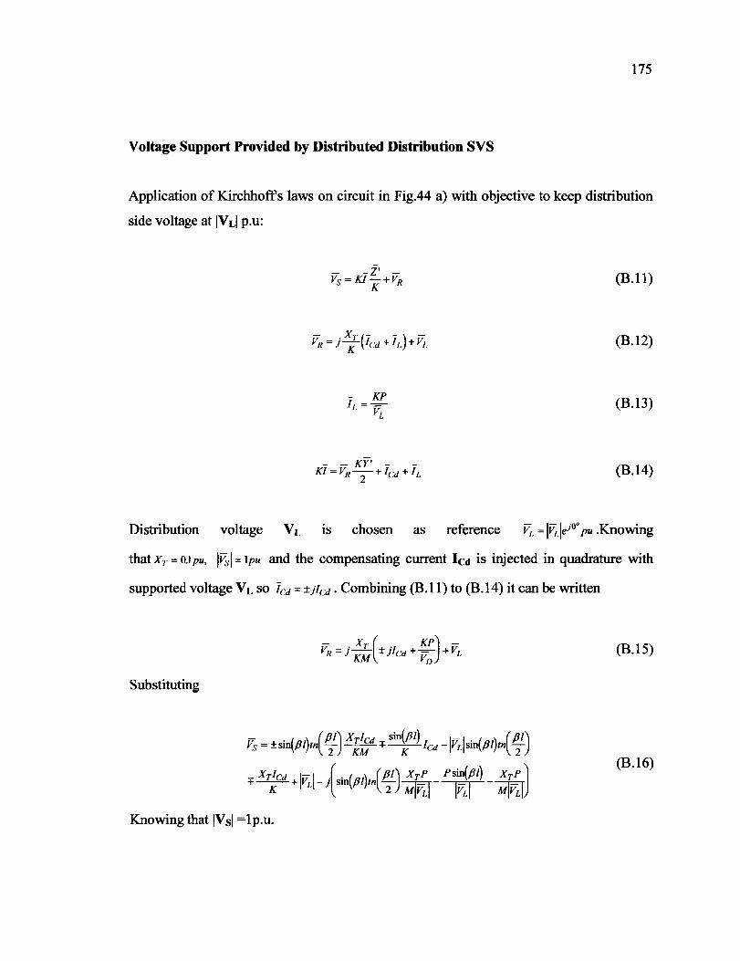
Reproduced with permission of the copyright owner. Further reproduction prohibited without permission.
175
Voltage Support Provided by Distributed Distribution SVS
Application of Kirchhoffs laws on circuit in Fig.44 a) with objective to keep distribution
side voltage at IVLI p.u:
- -Z' -Vs= Kl-+VR
K (B.ll)
(B.12)
(B.13)
(B.14)
Distribution voltage V L IS chosen as reference ~ = l~leJo• pu .Knowing
thatxr = O.Ipu, lfsl = lpu and the compensating current led is injected in quadrature with
supported voltage VL so led= ±jlcd. Combining (B.ll) to (B.14) it can be written
(B.15)
Substituting
- ( ) (Pl) Xrlcd sin(Pl} ~-~ ( ) (Pl) Vs= ±sin Pl tn T KM +-K-lcd- VL sin Pl t'\ T
- Xrlcd lv-I ·( . (Pl} (Pl) XrP Psin(Pl} XrP) +--+ L -1 sm tn - ~ 1 1 ~ K 2 MIVLI VL MIVLI
(B.16)
Knowingthat IVsl =lp.u.

Reproduced with permission of the copyright owner. Further reproduction prohibited without permission.
176
1 = [1Vil(1-sin(Pl)rn(~')) ± 1C: (sin(Pl)r{~1) ~ -sin(Pl)- ~) r
2 (B.17)
( . ( ) {P') XrP Psïn(Pl) XrP) + sm Pl t - .LI 1 1 1 .LI-~ 2 mrL VL miVL
The current ofdistributed SVSs needed to regulate VL is given by (B.18):
led = K X ( ') X K sin(Pl) + ,J- sïn(Pl)tn ~ ,J
lVi 1 ( 1- sin(p t}tn( ~1)) sin(Pt)+ Xr -sin(PI)tJ Pl) Xr
M '\2 M
(B.18)
1-~(sin(PI)J Pl) Xr -sin(Pl)- Xr)2
IVil2 '\ 2 M M

Reproduced with permission of the copyright owner. Further reproduction prohibited without permission.
APPENDIXC
THE PRINCIP AL P ARAMETERS OF TEST SYSTEM

Reproduced with permission of the copyright owner. Further reproduction prohibited without permission.
178
The principal simulation parameters are listed as:
A. Transmission Line
R = 0.0044 n/km, L=0.001 Hlkm, C=l.167e-08 F/km
B. Power Transformers
400 MVA, 315/25 kV, YgA, R1=0.0008 p.u.,X1=0.12 p.u. R2=0.0008 p.u., X2=0.12 p.u.
C. Load
1) Bus] a) Dynamic Load Po= 100 MW, Qo = 48 MV Ar, np =1,nq=3,kp=1,kq=-2.8 b) Motor Load Small Industrial Motors: 60 MW LF = 0.6, H =0.7, Rs = 0.19 n, Xs = 0.625 0, Xm = 20 n, Rr = 0.1125 0, Xr = 1.125 n. Load Torque:
1400 :z ~ 300 1 !:lOO ~
ro[rad/s] 0 T[kNm] 0
95 188 282. 377 1
10 39.8 92.7 160 1
~~~§§~~~~~~~~§:~~~~;;~~~
~lOO .. v .. l. so
0 lOO ISO lOO lSO lSO
5.-l (ndlsec]
oL-~~~~~~~~=-~~~ 0 lOO ISO lOO 2SO 300 lSO
s,-4 [ndlleC]
Fig.C 1. Small industrial motors equivalent S= 100 MV A

Reproduced with permission of the copyright owner. Further reproduction prohibited without permission.
2) Bus2 a) Dynamic Load Po= 130 MW, Q0 = 80 MV Ar, np=l.4, nq=1.4, kp=5.6, kq=4.2. b) Motor Load
Agricultural water pumps: 150 MW
179
LF = 0.7, H =0.8, Rs = 0.07 Q, Xs = 0.255 Q, Xm = 9.28 Q, Rr = 0.046 Q, Xr = 0.5 Q.
Load Torque:
3) Bus3
m [rad/sec] 0 95 188 282 377 T [kNm] 0 25.3 99.8 224 400
·~~--~--~----~--~----~--~--~~
_BOO & ~600 -
Percent rated voltage 100%
~400 ~
~~~~~~ 0 100 uo lOO 2.50 300 3.50
~300 = lOO • Cl a.
100
Speed (ndt-=1
oL-----~~~§5~~==~~~ 0 100 1.50 lOO 2.50 300 3.50
SJ-Ilndt-=1
Fig.C2.Agricultural water pump
a) Dynamic Load Po= 120 MW, Qo =55 MV Ar, np =1.2,nq=2.8,kp=O,kq=O b) Motor Load Large lndustrial Motors: 80 MW LF = 0.8, H =1.5, Rs = 0.08 Q, Xs = 0.42 Q, Xm = 23.75 Q, Rr = 0.056 Q, Xr = 1.06 Q. Load Torque:
m[rad/s] 0 95 188 282 377 T[kNm] 0 16.5 53.3 120 213

Reproduced with permission of the copyright owner. Further reproduction prohibited without permission.
180
~r-----r-----r-----r-----r-----r-----r-----r-~
Percent rated voltage 100%
0 0 100 ISO lOO 300 3SO
Fig. C3. Large industrial motors equivalent S= 100 MV A

Reproduced with permission of the copyright owner. Further reproduction prohibited without permission.
APPENDIXD
STEADY STATE SOLUTION FOR TEST SYSTEM

Reproduced with permission of the copyright owner. Further reproduction prohibited without permission.
182
Casel
Voltage support is provided with three SVS keeping voltages V RI. V R2 and V R2 at 1 p.u,
SVSs are connected on transmission level as shown on Fig.D.1 Compensating currents
are in quadrature with supported voltages
Fig.D.l
Compensating current can be found explicitly. Applying (6.19) it can be written:
(D.1)
(D.2)
(D.3)
Knowing that IVsl= IVRtl=l VR21= IVRJI= lp.u. and applying (6.15) load voltages can be
calculated as(D.4) to (D.7):
(D.4)

Reproduced with permission of the copyright owner. Further reproduction prohibited without permission.
183
(D.5)
(D.6)
(D.7)
The angles Ôï between transmission level voltages VRi and VR(i-I), and the angles Si
between load voltages Vu and transmission level voltages VRi are given with(D.8) to
(D.12):
(D.8)
(D.9)
(D.lO)
(D.ll)
(D.12)

Reproduced with permission of the copyright owner. Further reproduction prohibited without permission.
184
The alternative way of calculation reactive need is from phasor.
This is the case when voltages V Ri are kept at 1 p.u. with SVSs that are connected with
their own transformer at voltages they support. It means that the current drawn bu SVS is
in quadrature with voltage where it is connected.
13+14
Fig.D.2 Phasor diagram showing relations among the voltages and currents from voltage
VR2 to Vufor circuit from Fig.D.l.
From Pythagoras theorem to the right angle triangle fonned by VR3,Vu and j(XT4+ )4)1u
i(xr4 +X4)1ÏL4112
+IVz.l =l~l and~ =lh411Vz.41 (D.13)
(D.14)
(D.15)
(D.16)

Reproduced with permission of the copyright owner. Further reproduction prohibited without permission.
185
(D.17)
From eosine theorem (D.l8):
(D.18)
(D.19)
1- 1 ~ IL3 =-~-~
VL3 (D.20)
Reactive power supplied by SVS3 is (D.21):
(D.21)
Remarks:
The reactive power Q3 can be decomposed into three terms: frrst term provide half
reactive needs for line between voltages V 2 and V 3, second term represent reactive power
needed for power factor correction of the load current lu and third is for power factor
correction of load current lu. Physicly, it can be stated that on the bus where
compensator Q3 is connected (voltage V3) the compensator adjust reactive power so that
reactive power absorbed by the line and produced by the line + compensator match .
From point of view of the V 3 line is naturally loaded. Similar equations and explanation
can be deduced for other voltages.
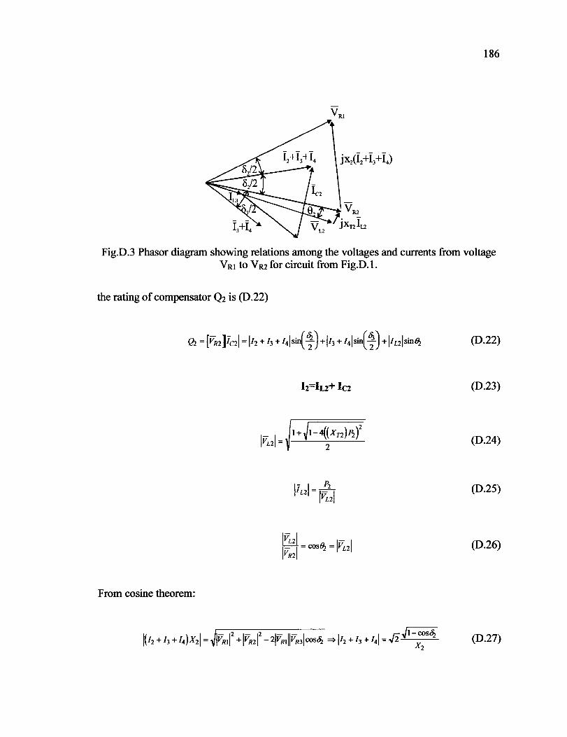
Reproduced with permission of the copyright owner. Further reproduction prohibited without permission.
186
Fig.D.3 Phasor diagram showing relations among the voltages and currents from voltage V RI to V R2 for circuit from Fig.D.l.
the rating of compensator Q2 is (D.22)
From eosine theorem:
1- 1 p2 IL2 =-~-1
VL2
lvd 1- 1 -~-l = cosfJ.! = VL2 VR2
(D.22)
(D.23)
(D.24)
(D.25)
(D.26)
(D.27)

Reproduced with permission of the copyright owner. Further reproduction prohibited without permission.
~ = arcsin(x2(P4 + P3 + 12))
Vs
187
(D.28)
Fig.D.4 Phasor diagram showing relations among the voltages and currents from voltage Vs to VR1 for circuit from Fig.D.l
Finally, the rating of compensator Q1 can be calculated from Fig. D.4 as (D.29):
(D.29)
1- 1 Il ILl=-,-, VLI
(D.30)
(D.31)
ru 1-1 1- l = costl = VLI VRI
(D.32)
(D.33)
1/Xll -- ,- 12 ,-,2 ,- ,,-, l l r;; ~1- cos~ VRI + Vs -2 VRI Vs cos~ => 1 = v2-'------'--Xl
(D.34)

Reproduced with permission of the copyright owner. Further reproduction prohibited without permission.
188
and lt=lu+ let
Resume: each compensator correct power factor for the currents leaving bus where it is
connected and provide the reactive needs for the half of the path between the bus where it
keep voltage at 1 p.u and next bus where the next compensator keep its voltage at 1 p.u.
It can be said that compensator balance reactive needs on the point of its coupling with
grid.
Case 2:
Voltage support is provided on distribution level with 4 SVS as illustrated in Fig.D.5
Fig.D.5
Compensation Requirement
To calculate reactive power needed for distribution side voltage regulation (VLi =1 p.u.)
first transmission si de voltages V Ri (i= 1 , ... N) has to be calculated. They are calculated
from set of implicit equations as shown in ( 6.26) and for each node it can be written
(D.35)
(D.35)

Reproduced with permission of the copyright owner. Further reproduction prohibited without permission.
where ÔÏ ÏS power angle between VOltages V R(i-1) and V Ri, iji ÏS power angle between
voltages V Ri and V Li
it is known that IVui=IVul =!Vul =!Vul lp.u.
IVRol = IVsl=l p.u.
The power angles can be calculated from (D.36) and (D.37)
N
189
P = L P; where P is total power transferred over the line and Pi is power supplied to i-th i=]
load center. Soit can be written(D.36) and (D.37):
and Vu= 1 p.u. so
The power transferred through i-th segment of the line is (C.38):
lvR(i+]llvR;I2 -C~:kr xi+I
2
jvR(i+I)l!vR;I
substituting (D.37) and (D.39)into (D.35) we obtain (D.40):
(D.36)
(D.37)
(D.38)
(D.39)
(D.40)

Reproduced with permission of the copyright owner. Further reproduction prohibited without permission.
190
what gives set ofN algebraic implicit equations allowing to calculate voltages V Ri .In this
case Gauss-Seidel method has been used.
The current through each segment of the line can be computed from eosine
theorem(D.41 ):
(D.41)
the current through i-th substation can be calculated from eosine theorem applied on
triangle formed by voltages V Ri, V Li and voltage drop across substation transformer:
(D.42)
and finally compensating current Ici can be calculated from Pythagoras's theorem(C.43):
(D.43)

Reproduced with permission of the copyright owner. Further reproduction prohibited without permission.
REFERENCES
[1] C.W. Taylor, Power System Voltage Stability, New York: McGraw-Hill, 1994.
[2] S.H.Horowitz and A.G. Phadke "Boosting Immunity to Blackouts", power & energy magazine, Sept/Oct. 2003, pp.47.
[3] D. Novosel, M. M. Begovic and V. Madani, "Shedding Light on Blackouts", IEEE power & energy magazine, Jan./Feb. 2004, pp.32.
[4] Bruce E. Wollenberg, "From Blackout to Blackout", IEEE power & energy magazine, Jan./Feb. 2004, pp.88.
[5] IEEE Special Publication, "Voltage Stability of Power Systems: Concept, Analytical Tools and Industry Experience", 90TH0358-2-PWR,1990.
[6] IEEE Special Publication, "Suggested Techniques for Voltage Stability Analysis", 93TH0620-5-PWR, 1993.
[7] IEEE Special Publication, "Voltage Stability Assessment: Concepts, Practices and Tools", IEEE Press 2003.
[8] R.H. Lasseter, "Control of Distributed Resources," in Proc. Bulk Power Systems Dynamics and Control, pp. 323-329, Greece, Aug. 23 - 28, 1998.
[9] T.J. Miller, Reactive Power Control in Electric Systems, New York: Wiley Interscience, 1982.
[10] L.Gyugyi, "Reactive Power Compensation and Control by Thyristor Circuits" IEEE 1976 PESC Conference Record, pp 174-184.
[11] R. Esliger, Y. Hotte and J. C. Roy, "Optimisation of Hydro Quebec's 735 kV Dynamic Shunt Compensated System Using Static Compensators on a Large Scale." PES winter Meeting, New York, Feb 1978.
[12] D. McGillis, N. Hieu Huynh and G. Scott "Role of Static Compensation in Meeting AC System Control Requirements with Particular Reference to the James Bay System", lEE Proc., Vol.l28, No.6. pp. 389, Nov 1981.
[13] Ooi. B.T., Steady State Stability and Subsynchronous Resonance of Shunt Capacitor Compensated Transmission Lines", IEEE Transaction on Power Apparatus and System, vol.PAS-101, Sept.1982, no.9,pp.3269-3275.

Reproduced with permission of the copyright owner. Further reproduction prohibited without permission.
192
[14] R. Mathur, " Static Compensators for Reactive Power Control", Canadian Electrical Association 1984.
[15] L. Gyugyi," Fundamentals of Thyristor Controlled Static V Ar Compensators in Electric Power System application" IEEE Special Publication 87TH0187-5-PWR, 1987.
[16] N. G. Hingorani and L. Gyugyi, Understanding FACTS: Concepts and Technology of Flexible AC Transmission Systems, Wiley IEEE Press, December 1999.
[17] J. P. Ramos and H. Tyll, "Dynamic Performance of a Radial Weak Power System with Multiple Static V Ar Compensators", IEEE Trans. on Power Systems Vol.4, No.4 October 1989.
[18] R. Grunbaum, M. Halonen and S. Rudin "ABB Static Var Compensator Stabilizes Namibian Grid Voltage" ABB Review, 2003, pp 43-48.
[19] H. Akagi, Y. Kanazawa and A. Nabae, "Instantaneous Reactive Power Compensators Comprising Switching Deviees without Energy Storage Components," IEEE Trans. lnd. Applicat., vol. IA-20, no. 3, May./June. 1984, pp. 625-630.
[20] C.W.Edvards et al. "Advanced Static V Ar Generator Employing GTO Thyristors", IEEE PES Winter Power Meeting, Paper No. 38WM109-1,1988.
[21] H.Mehta, T.W.Cease and L.Gyugyi, "Static Condenser for Flexible AC Transmission System" EPRI Flexible AC Transmission System (FACTS) conference, 18-20 May, 1992 Boston, MA.
[22] E.Larsen, N. Miller S. Nilsson and S. Lindgren. "Benifits of GTO-Based Compensations System for Electric Utility Applications, IEEE Trans. Power Delivery, vol.7, no.4 pp. 2056-2062, Oct.1992.
[23] L.Gyugyi, "Dynamic Compensation of AC Transmission Lines by Solid State Synchronious Voltage Source", IEEE Trans. Power Delivery, vol.9, no.2 pp. 904-911, April.1994.
[24] C. Schauder, M. Gerhardt, E. Stacey, T. Lemak, L. Gyugyi, T.W. Cease and A. Edris, "Development of a +/-1 00 MV AR Static Condenser for Voltage control of Transmission Systems" IEEE PES 1994 Summer Meeting, San Francisco, CA July24-28.

Reproduced with permission of the copyright owner. Further reproduction prohibited without permission.
193
[25] K.K. Sen, "STATCOM-Static Synchronous Compensator : Theory, Modeling and Applications", IEEE, PES Winter Meeting 1999, Vol.2 pp.1177-1183.
[26] Paserba J., Larsen E., Lauby M., Leonard D., Nauman S., Miller N and Sener F.,"Feasibility Study for a Distribution-Leve! STATCON," FACTS Application, 1996, pp.8-22, 8-28, IEEE Catalog Number: 96TP 116-0.
[27] Koessler R, Fardanesh B., Henderson M.l. and Adapa R., "Feasibility Studies for STATCOM Application in New York State," pp. 8-46, 8-51, FACTS Application, 1996, pp.8-52, 8-58, IEEE Catalog Number: 96TP 116-0.
[28] Clark K., Doyle W.A., Sener F. and Smead M." STATCON Application StudyPotential Solution to Loss In-Feed", FACTS Application, 1996, pp.8-91, 8-96, IEEE Catalog Number: 96TP 116-0.
[29] W. McMurray, "Series Connection of Gate-Turnoff Thyristors" EPRI Report EL-5332, August 1987.
[30] A. Nabae, 1. Takahashi and H. Akagi, "A New Neutral-Point-Clamped PWM Inverter," IEEE Trans. Ind. Applicat., vol. IA.17, no. 5, Sept./Oct. 1981 pp. 518-523.
[31] N. S. Choi, J. G. Cho, and G. H. Cho, A General Circuit Topology of Multilevel Inverte, IEEE 22nd Annual Power Electronic Specialist Conference, 1991, pp.96-103.
[32] P. M. Bhagwat and V. R. Stefanovic, Generalized Structure of a PWM Multilevel Inverte IEEE Trans. Ind. Applicat., vol. 19, no. 6,, Nov./Dec. 1983, pp. 1057-1069.
[33] Xiaoming Yuan and lvo Barbi, Fundamentals of a New Diode Clamping Mu/ti/eve/ Inverter IEEE Trans. Pow. Electronics, vol. 15, no. 4, pp. 711-718, July2000.
[34] S. Iida, S. Masukawa and Y Kubuta, et al., Improved Voltage Source Inverter With 18-Step Output Waveformes, IEEE Industry Applications Magazine, Jan/Feb. 1998.
[35] Lai S. and Peng F. Z., Mu/ti/eve/ Converters - A New Breed of Power Converters, IEEE Trans. lnd. Applicat., vol. 32, May/June 1996, no.3, pp 509-517.

Reproduced with permission of the copyright owner. Further reproduction prohibited without permission.
194
[36] Menzies W. and Zhuang, Y.: Advanced Static Compensation Using a Mu/ti/eve/ GTO Thyristor Inverter, IEEE Transaction on Power Delivery, vol.lO, April 1995, no.2, pp. 732-738.
[37] Ekanayake B. and Jenkins N.: A Three-level Advanced Static Var Compensator, IEEE Transaction on Power Delivery, vol.ll, Jan.1996, no.l, pp. 540-545.
[38] Hochgraf C. and Lasseter R. H.: A Transformer-less Static Synchronies Compensator Employing a Mu/ti-leve/ Inverter, IEEE Transaction on Power Delivery, vol.l2, April1997 no.2, pp. 881-887.
[39] S.Kincic, A.Chandra and S.Babic "Five Level, Diode-Clamped Voltage Source Inverter and Its Application in Reactive Power Compensation" LESCOPE 2002, July 26-28, 2002, , pp.86-92, Halifax, Nova Scotia, Canada.
[40] S.Kincic, A.Chandra and S.Babic "Power Factor Correction of Single Phase and Three Phase Unbalanced Loads using Multilevel Inverter" LESCOPE 2001, July 11-13, 2001,pp.131-138, Halifax, Nova Scotia, Canada.
[41] Vijay K. Sood, " Position Paper on FACTS Technology" Canadian Electricity Association, February 1996.
[42] B. T. Ooi and X. Wang, " Boost Type PWM-HVDC Transmission System," IEEE Transaction on Power Delivery, vol.6, Oct.1991, no.4, pp. 1557-1563.
[43] X. Wang, Shu-Zu Dai and B.T.Ooi, "A series Capacitive Reactance Compensator Based on Voltage Source PWM Converter", presented at IEEE-lAS Annual Meeting, pp. 918-924, Sept./Oct 1991.
[44] B.T. Ooi, S.Z. Dai and F.D. Galiana, "A Solid State PWM Phase Shifter", IEEE Transaction on Power Delivery, vol.8, Apr.1993, no.2, pp. 573-579.
[45] B.T. Ooi and S.Z. Dai "Series Type Solid State Static Var Compensator", IEEE Transaction on Power Electronics, vol.8, Apr.1993, no.2, pp. 164-169.
[46] Mwinyiwiwa B., Wolanski Z and, Ooi B.T.: High Power Switch Mode Linear Amplifiers for Flexible AC Transmission Systems, IEEE Transaction on Power Delivery, vol.11, Oct.1996, no.4, pp. 1993-1998.
[47] "The Hagfors SVC Light: a world fust" ABB utilities AB Power System
[48] "The Moselstahlwerk SVC light" ABB utilities AB Power System

Reproduced with permission of the copyright owner. Further reproduction prohibited without permission.
195
[49] W.K.Wong, D.L.Osbom and J.L.McAvoy, "Application of Compact Static V Ar Compensators to Distribution System,"IEEE Trans. Power Delivery, vol. 5,No.2, pp. 1113-1120, Apr. 1990.
[50] R.J.Koessler,"Dynamic Simulation of Static V Ar Compensator in Distribution Systems," IEEE Trans. Power Sysy, vol. 7,No.3, pp. 1285-1291, Aug. 1992.
[51] A.E.Hammad and M.Z. El-Sadek," Prevention ofTransient Voltage Instabilities due to Induction Motor Loads by Static V Ar Compensators", IEEE Trans. Power Systems, vol. 4, No.3, pp.ll82-1190, August 1989.
[52] Paserba J.J., Leonard D.J., Miller N.W, Nauman S.T., Lauby M.G., Lauby M and Sener F .P, "Coordination of a Distribution Level Continuously Controlled Compensation Deviee with Existing Substation Equipment for Long Term V Ar Management"", IEEE Trans. Power Delivery, vol. 9, pp. 1034-1040, Apr. 1994.
[53] J. CR. Clouston and J.H.Gumey," Field Demonstration of a Distribution Static Compensator Used to Mitigate Voltage Flicker," PES Winter Meeting 2002.
[54] S. Kolluri," Application of Distributed Superconducting Magnetic Energy Storage System (D-SMES) in the Entergy System to Improuve Voltage Stability," PES Winter Meeting 2002.
[55] John A.Diaz de Leon ll and C.W. Taylor," Understanding and Solving ShortTerm Voltage Stability Problems," PES Winter Meeting 2002.
[56] S.Kincic and A. Chandra, "Distribution Level STATCOMs (DSTATCOMs) for Load Voltages Support", LESCOPE 2003,7-9 May, Montreal
[57] S.Kincic and A. Chandra, "Impact of Distributed Compensators on Power System Voltages", CCECE 2003,5-7 May, Montreal.
[58] B.T.Ooi, S.Kincic, X.Wan, D.McGillis, A.Chandra, F.D. Galiana and G. Joos, "Distributed Static V Ar Systems for Regulated Voltage Support in Load Centers, "PES General Meeting, 13-18 July,2003, Toronto.
[59] S.Kincic, X.Wan, D.McGillis, A.Chandra, B.T.Ooi, F.D. Galiana and G. Joos, "Voltage Support by Distributed Static V Ar Systems " IEEE Trans. on Power Delivery, Vol.20.No.2,April2005, pp1541-1549.
[60] Y. Chen, B. Mwinyiwiwa, Z. Wolanski and B. T. Oou," Regulating and Equalizing DC Capacitans Voltages in Multilevel Statcom," IEEE Trans. Power. Delivery, vol. 12, no. 2, April. 1997, pp. 901-907.

Reproduced with permission of the copyright owner. Further reproduction prohibited without permission.
196
[61] S. Kincic "Onduleur à nivaux multiples et son application en compensation de puissance reactive" Mémoire de la maîtrise, ETS, Mai 2000
[62] S.Kincic, A.Chandra, B.N.Singh and P.Rastgoufard "Real Time Simulation With Two Novel Control Algorithms" lOth IEEE Mediterranean Conference on control Automation,. Portugal, 2002
[63] S.Kincic, A.Chandra, Z.Huang and S.Babic "Simulation Study on Enhancement of Maximum Power Transfer Capability of Long Transmission Line With Midpoint Sitting STATCOM for Voltage Support" EPE-PEMC 2002 Cavtat &Dubrovnik.
[64] B.T. Ooi and X. Wang,"Voltage Angle Lock Loop Control ofBoost Type PWM Converter for HVDC Application,"IEEE Trans. power Electronics, Vol.5No.2,pp.229-235, Apr.l990.
[65] Ooi B. T., Kazerani M., Wolanski Z., Galiana F.D., McGillis D., Joos G. and Marceau G, "Midpoint Siting of FACTS Deviees in Transmission Lines," IEEETransaction on Power Delivery, vol.l2, Oct. 1997, no.4, pp.l717-1722.
[66] Z. Huang and B.T. Ooi, "Power Transfer Capability of Long Transmission Lines with Midpoint Sited Facts and HVDC," IEEE Power Engineering Review, Vol.22, No.5, pp. 51-53, May 2002.
[67] Z. Huang, B.T. Ooi, L.A. Dessaint and F.D. Galiana, "Exploiting Voltage Support ofVoltage Source HVDC," lEE Proceedings-Generation, Transmission andDistribution, Vol.l50, No.2, pp.252-256, Mar.2003.
[68] K. K.ahle, J. Pedersen, T. Larsson and M.M de Oliveira "The New 150 Mvar kV Static V ar Compensator at CERN: Background, Design and Commissioning" 17th International Conference on Electricity Distribution, Barcelona, 12-15 May 2003.
[69] R.M. Mathur and R. K. Varma, Thyristor-Based FACTS Controllers for ElectricalTransmission Systems, IEEE Press, 2002.
[70] J. Van Coevering, J. P. Stovall, R. L. Hauth, P.J. Tatro, B. D. Railing and B. K. Johnson," The Next Generation ofHVDC- Needed R&D, Equipment Costs and Cost Comparisons", Proceedings of EPRI Conf. on Future of Power Delivery, Washington DC, April 1996.
[71] D. McGillis,"Principles and practice of transmission system planing",4th Int. Tesla Symp. Belgrade, Yugoslavia, Sept.1991.
Reproduced with permission of the copyright owner. Further reproduction prohibited without permission.
197
[72] Power System Simulator-HYPERSIM: User's Manual, DMNU-5700-1.3A, TEQSIM International INC., June 1999.
[73] IEEE Task Force on Load Representation for Dynamic Performance, "Load Representation for Dynamic Performance Analysis", IEEE Trans. on Power Systems, Vol.8, No.2, May 1993.
[74] IEEE Task Force on Load Representation for Dynamic Performance, "Standard Load Models for Power Flow and Dynamic Performance Simulation", IEEE Trans. on Power Systems, Vol.lO, No.3, August 1995.
[75] B. R. Williams, W. R. Schmus and D. C. Dawson, " Transmission Voltage Recovery Delayed by Stalled Air Conditioners", IEEE Trans. on Power Systems, Vol.7, No.3, pp.1173-1178, August 1992.
[76] John W. Shaffer, "Air Conditioner Response to Transmission Faults" IEEE Trans.on Power Systems, Vol.12, No.2, pp.614-621, May 1997.
[77] Walter A. Elmore, "Protective Relaying Theory and Application" ABB Power T&D Company Inc. Relay Division, Coral Springs, Florida 1994 pp.334.
[78] S.Kincic, B.T.Ooi , D.McGillis and A.Chandra,,"Voltage Support of Radial Transmission Lines by V Ar Compensation at Distribution Buses", ProceedingsGeneration, Transmission and Distribution Vol. 153, pp.5 -58, Jan. 2006.