ece 298 modeling and optimization of vlsi circuits and systemseda.ee.ucla.edu/intro.pdf · ece 298...
TRANSCRIPT
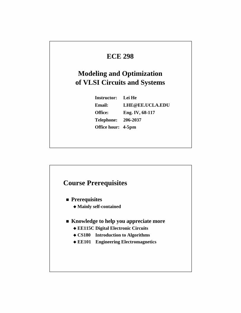
ECE 298
Modeling and Optimization of VLSI Circuits and Systems
Instructor: Lei He
Email: [email protected]
Office: Eng. IV, 68-117
Telephone: 206-2037
Office hour: 4-5pm
Course Prerequisites
n PrerequisitesuMainly self-contained
n Knowledge to help you appreciate moreuEE115C Digital Electronic Circuits
uCS180 Introduction to Algorithms
uEE101 Engineering Electromagnetics

References
n Cong-He-et al, Performance Optimization of VLSI Interconnect Layout, Integration, the VLSI Journal21 (1996) 1--94.
n Selected papers from major circuit and CAD conferences and journals
n Raminderpal Singh, “Signal Integrity Effects in Custom IC and ASIC Designs,” IEEE Press, 2002.
n ACM IEEE Design Automation Conference (DAC)
n International Conference on Computer Aided Design(ICCAD)
n IEEE International Symposium on Circuits and Systems (ISCAS)
n Design, Automation and Test in Europe (DATE)
n Asia and South Pacific Design Automation Conference (ASP-DAC)
n International symposium on physical design (ISPD)
n IEEE Transactions on CAD of Circuits and systems (TCAD)
n ACM Trans. on Design Automation of Electronic Systems (TODAES)
n IEEE Transactions on Circuits and Systems (TCAS)
n IEEE Trans. on VLSI Systems (TVLSI)
Related VLSI CAD Conferences and Journals

Grading Policy
n Homework 20%n Quiz and Midterm 20%n Paper presentation 10%
n Use transparencies or video projector
n Graded by fellow students
n Term project 50%n Bonus points
u For active participation
n Grade A for score > 85
Term Project
n One of the following:u Survey of selected papers (1 person, at most 40
points)
u Programming project (2 persons in a term)
uWriting requirements FIn a conference paper style

Course Outline
n Overview and Introduction (1 lecture)
n Interconnect Extraction and Modeling (3 lectures)
n Timing models, Delay Calculation, and Timing Analysis (2 lectures)
n Wireload model, logic effort and fanoutoptimization (2 lectures)
n Interconnect Synthesis and Routing Optimization (2 lectures)
Course Outline
n Noise Modeling, Avoidance and Control (3 lectures)
n Power Supply Modeling and Optimization (2 lectures)
n High-level Area/Power Estimation and Layout Planning (2 lectures)
n System-level Interconnect design** (1 lecture)

Skills to Learn
n Interconnect modeling and designn A course parallel to EE216M
n Algorithm / Programming / writing / presentation
Course Web Site
n Examples of previous projectsn http://eda.ece.wisc.edu/ece902.html
n Course websiten http://eda.ee.ucla.edu/ee298.html

Overview
n Moore’s Law
n CMOS scaling theory
n Interconnect performance implied by NTRS’97
n Need for a new design paradigm
Basic Components In VLSI Circuits
n Devicesu Transistorsu Logic gates and cellsu Function blocks
n Interconnectsu Local signalsuGlobal signalsuClock signalsu Power/ground
networks
Pad Metal
Via Metal 2
I/OData Path
ROM/RAM
PLA
A/D ConverterRandom logic

Storageelement
Combinational Logic
Clock Period td-gates + td-interconnects + tskew + tsu + tds≥td-gates = gate delay in comb. logic
td-interconnects = interconnect delay in comb. logic
tskew = clock skew
tsu = set-up time
tds = delay within storage elements
Determining Factors of System Performance
Interconnect
delay
nTechnology Trends:
uDeep sub-micron design: < 0.18 micron CMOS technology
uHigh-Speed : > 500 MHz ~ 5 GHz
nImpact on VLSI System Design
u Interconnect delay becomes the dominating factor in system performance
oConsumes 50%-70% clock cycle
uDistributed nature of interconnects becomes significant
oBecomes distributed RCL circuits or lossy transmission lines.
Interconnect-Driven Design
Importance of VLSI Interconnect Design

Technology (um) 0.25 0.18 0.15 0.13 0.10 0.07Year 1997 1999 2001 2003 2006 2009
# transistors 11M 21M 40M 76M 200M 520MOn-Chip Clock (MHz) 750 1200 1400 1600 2000 2500
Area (mm2) 300 340 385 430 520 620Wiring Levels 6 6-7 7 7 7-8 8-9
Moore’s Law and NTRS
n Moore’s Lawu The min. transistor feature size decreases by 0.7X every three
years (Electronics Magazine, Vol. 38, April 1965)u True in the past 30 years!
n National Technology Roadmap for Semiconductors (NTRS’97)
Assumptions:aAll horizontal & vertical dimensions of a transistor( W, L,tgox, Xj) are reduced by S
aAll voltages ( Voo, VTN, VTP ) are reduced by S
a Substrate doping (Nsub) is increased by S
a (VTN, VTP: threshold voltages of N and P transistors)
Ideal Scaling of MOS Transistors
Figure 1.1 Metal-Oxide-Semiconductor Field-Effect Transistor (MOSFET).The main dimensions that determine device properties are gate oxide thickness
tgox; gate length L, gate width W; and junction depth Xj
Leff
W
S D
tgoxXj
G
B

TABLE 1.1 Scaling of MOS Transistors
Parameter Scaling FactorDimensions (W, L, tgox, Xj) 1/S
Substrate doping (NSUB) S
Voltages (VDD , VTN, VTP) 1/S
1/S
1/S
1
1/S
Power-dissipation per gate (P=IV) 1/S2
1/S3
Area per device (A=WL) 1/S2
Power-dissipation density (P/A) 1
))V(Vt
å
L
W(I deviceper Current 2
TDDgox
oxDS −∝
))V(Vt
WLå(C ecapacitanc Gate 2
TDDgox
oxg −=
)I
V(R resistance-on Transistor
DS
DDtr ∝
)CRI
VC(ô delay date Intrinsic gtr
av
g=
∆=
ô)(P gateper product delay-Power ×
geometric dimentsions of the transistor
FIGURE 2.2 I-V characteristics of an nMOS transistor
Ios= ( )[ ]( )
−=
−−
2
VVâ
/2VVVVâ
o
tngsn
2osostngsn
tngsds
tngsds
tngs
VVV
VVV
VV
−≥
−≤
≤ (Cut-off)
(Linear in terms of VGS)
(Saturation,
independent of VDS)
L
w..cìâ goxnn = Gain Factor
gox
ox
ô
å
Current Through an n-channel MOS Transistor
electron mobility
IDSLinear
VGS
VDS
VDS= VGS-Vττ

Assumptions:a Cross Sectional dimensions ( Wint, Hint, Wsp, Tox) are reduced by S
a Die Size and global interconnection Lengths are increased by Sc
Ideal Scaling of VLSI Interconnects
Figure 1.2 Basic interconnection parameters
lint
wsp wint
Hint
tox
Parameter Scaling FactorCross sectional Dimensions (W int , H int , W sp, t ox) 1/S
S2
1
RC constant per unit length (R intC int) S2
Local interconnection length (l loc ) 1/S
1
Die size (D C ) SC
Global interconnection length ( l int) SC
S2(SC)
2
Transistor line time of flight (l int /v c) SC
)HW
1ñ(R
intintintint = lengthunit per Resistance
)lC(R 2locintint delay RC ctioninterconne Local
)t
W(C
ox
intoxint ε= lengthunit per eCapacitanc
)lC(R 2intintint delay RC ctioninterconne Global
Table 1.2 Scaling of Local and Global Interconnections

Ideal Qussi-Ideal Constant-R Generalized
Scaling Scaling Scaling ScalingThickness (Hint) 1/S 1/SH
Width (Wint) 1/S 1/S 1/SW
Separation (Wsp) 1/S 1/S 1/Ssp
Insulator thickness (tox) 1/S 1/Sox
Length (lloc) 1/S 1/S 1/S
Resistance (Rint) S 1 SWSH/S
Capacitance to substrate 1/S 1/S3/2
Sox/SSW
Capacitance between lines 1/S Ssp/SSH
RC delay (T) 1Voltage drop (IR) 1 1/S SWSH/S
2
Current density (J) S 1 SWSH/S
Parameter
S1/
2HW /SSS≈
1/S≈
1/S≈
1/S≈1/S≈
S1/
S1/
S1/
S1/S1/
S1/
S1/S
S
S1/≈
Ideal Qussi-Ideal Constant-R Generalized
Scaling Scaling Scaling ScalingThickness (Hint) 1/S 1/SH
Width (Wint) 1/S 1/S 1/SW
Separation (Wsp) 1/S 1/S 1/Ssp
Insulator thickness (tox) 1/S 1/Sox
Length (lloc) 1/S 1/S 1/S
Resistance (Rint) S 1 SWSH/S
Capacitance to substrate 1/S 1/S3/2
Sox/SSW
Capacitance between lines 1/S Ssp/SSH
RC delay (T) 1Voltage drop (IR) 1 1/S SWSH/S
2
Current density (J) S 1 SWSH/S
Parameter
S1/
2HW /SSS≈
1/S≈
1/S≈
1/S≈1/S≈
S1/S1/
S1/
S1/S1/
S1/
S1/S
S
S1/≈
not good for packing density
Local Interconnects under Different Scaling RulesTable 5.1 Scaling of Local Interconnections
Ideal Constant Constant Generalized
Scaling Dimension Delay Scaling
Thickness (Hint ) 1/S 1 SC 1/S H
Width (Wint) 1/S 1 SC 1/S W
Separation (Wsp) 1/S 1 SC 1/S sp
Insulator thickness (tox) 1/S 1 SC 1/S ox
Length (lloc) S C SC SC SC
Resistance (Rint ) S2S C SC 1/S C SWS HSC
Capacitance (Cint ) S C SC SC
RC delay (T) S2(SC)
2(SC)
21 SWSH(SC)
2
Parameter
/SSS
CS≈
1/S
Global Interconnects under Different Scaling Rules
Table 5.2 Scaling of Global Interconnections
S: Scaling factor for device dimensions.
Sc:Scaling factor for chip size

Interconnect Parameters from NTRS’97
Technology (um) 0.25 0.18 0.15 0.13 0.10 0.07
Res. ρρ (uΩΩ /cm) 3.3 2.2 2.2 2.2 2.2 1.8
Dielectric constant 3.55 2.75 2.25 1.75 1.75 1.5
Min. wire width 0.25 0.18 0.15 0.13 0.10 0.07
Min. wire spacing 0.34 0.24 0.21 0.17 0.14 0.10
Metal aspect ratio 1.8:1 1.8:1 2.0:1 2.1:1 2.4:1 2.7:1
Via aspect ratio 2.2:1 2.2:1 2.4:1 2.5:1 2.7:1 2.9:1
Vdd (V) 2.15 1.65 1.35 1.35 1.05 0.75
Capacitance Computation
n Capacitance extraction using a 3D field solver (FastCap)
C fCa
Cx

Derived Interconnect & Device ParametersTechnology (um) 0.25 0.18 0.15 0.13 0.10 0.07
Ca (aF/um) 29.0 21.2 16.2 12.0 14.4 8.56
Cf (aF/um) 41.8 30.2 24.8 18.3 14.1 14.8
2X min.
width &
spacing Cx(aF/um) 71.0 58.3 49.4 42.8 45.3 41.6
Ca (aF/um) 73.5 53.6 40.6 30.0 26.6 19.5
Cf (aF/um) 63.5 47.3 38.4 28.5 28.2 23.6
5X min.
width &
spacing Cx(aF/um) 18.3 16.9 15.4 14.8 16.5 16.7
0.17 0.12 0.11 0.085 0.070 0.042
1.71 1.86 2.26 2.25 2.39 2.42
Buffer input cap. (fF)
Buffer Rd (x10KΩΩ )
Buffer intrin. delay (ps) 70.5 51.1 48.7 45.8 39.2 21.9
Impact of Interconnect Optimization on Future Technology Generations
0.01
0.1
1
10
0.25 0.18 0.15 0.13 0.1 0.07Technology (u m)
Del
ay (
ns)
1mm
2cm DS
2cm BIS
2cm BISWS
Intrinsic gatedelay

Impact of Interconnect Optimization on Future Technology Generations
Technology (um) 0.25 0.18 0.15 0.13 0.10 0.071mm (ns) 0.059 0.049 0.051 0.044 0.052 0.0422cm DS (ns) 2.589 2.48 2.65 2.62 3.73 4.672cm BIS (ns) 1.779 1.55 1.59 1.51 1.74 1.552cm BISWS (ns) 0.895 0.793 0.77 0.7 0.77 0.672
Significance of Coupling Capacitance
0
0.2
0.4
0.6
0.8
1
0.25 0.18 0.15 0.13 0.1 0.07
Technology Generation (um)
Cx/Ctotal
Min. Spacing
2x Min. Spacing

Coupling Noise
0.000
0.050
0.100
0.150
0.200
0.250
0.300
0.350
250 180 150 100 70Technology (nm)
Noi
se (%
Vdd
) a pair of in-phase aggressors
one aggressor
a pair of skewed
Coupling noise from two adjacent aggressors to the middle victim wire with 2x min. spacing. Rise time is 10% of project clock period.
•Capacitive coupling depends strongly on both spatial and temporal relations!
Implications
n Communication is more expensive than computation
n Interconnect performance has become the bottleneck of the overall circuit/system performance
n Interconnect modeling and optimization has become very difficult due to the distributed nature of interconnects and their spatial and temporal interactions
n A new design paradigm/flow is needed to handle interconnect-dominated designs in the future

System Specification
Functional Design
Logic Design
Circuit Design
X=(AB*CD)+(A+D)+(A(B+C))
Y=(A(B+C))+AC+D+A(BC+D))
VLSI Design Cycle
Physical Design
Fabrication
Packaging
VLSI Design Cycle (cont.)

Transistors/Cells
Interconnection
Interconnection
Transistors/Cells
Need A New Paradigm for VLSI Design
Conventional Approach New Approach
Interconnect-Driven Design
Program
Data
Data/Object
Program
Paradigm Change in Software Design
Conventional Approach New Approach
Data Base Design
Object-oriented design

Summary
n Technology scaling according to Moore’s Law has been the driving force behind the exponential growth of the semiconductor industry
n Interconnect (esp. global interconnect) performance and noise have become the bottleneck of the overall system design
n Interconnect modeling and optimization has become very important, yet difficult
n A new design paradigm is needed for interconnect-driven (or interconnect-centric) design
Homework (due next Thursday)
n Read ITRS ORTC and Interconnectn ORTC: overall roadmap technology characteristics
n http://public.itrs.net/Files/2000UpdateFinal/2kUdfinal.htm
n Find two categories of differences between NTRS’97 (in this notes) and ITRS’00 interconnect characteristics, and explain reasons for such changes