ece 2133 electronic circuitsstaff.iium.edu.my/zahirulalam/courses/ece2133/feedback.pdf · ece 2133...
TRANSCRIPT
ECE 2133
Electronic Circuits
Dept. of Electrical and Computer Engineering
International Islamic University Malaysia

Chapter 12
Feedback and Stability

Introduction to Feedback
1-4
© Electronic Circuits
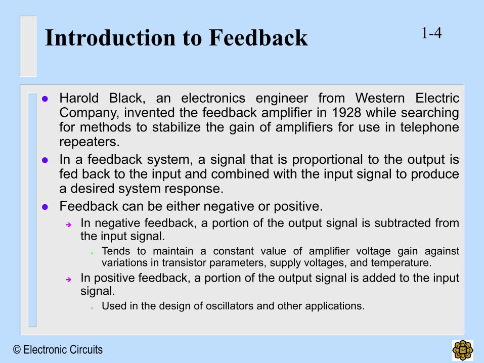
Introduction to Feedback
Harold Black, an electronics engineer from Western Electric Company, invented the feedback amplifier in 1928 while searching for methods to stabilize the gain of amplifiers for use in telephone repeaters.
In a feedback system, a signal that is proportional to the output is fed back to the input and combined with the input signal to produce a desired system response.
Feedback can be either negative or positive.
In negative feedback, a portion of the output signal is subtracted from the input signal.
Tends to maintain a constant value of amplifier voltage gain against variations in transistor parameters, supply voltages, and temperature.
In positive feedback, a portion of the output signal is added to the input signal.
Used in the design of oscillators and other applications.
1-5
© Electronic Circuits
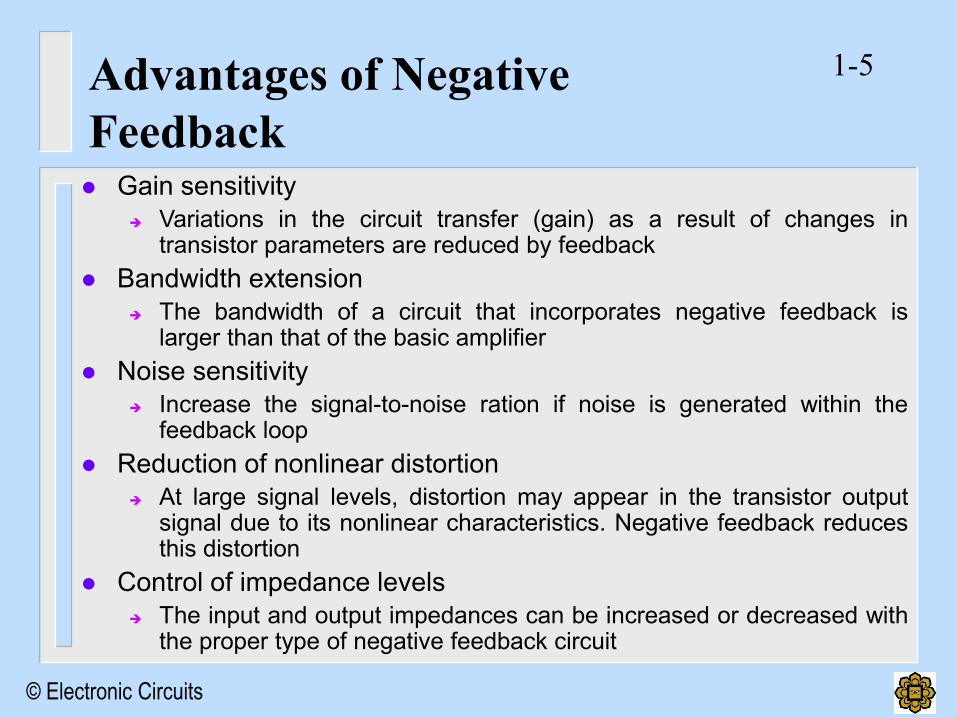
Advantages of Negative
Feedback Gain sensitivity
Variations in the circuit transfer (gain) as a result of changes in transistor parameters are reduced by feedback
Bandwidth extension
The bandwidth of a circuit that incorporates negative feedback is larger than that of the basic amplifier
Noise sensitivity
Increase the signal-to-noise ration if noise is generated within the feedback loop
Reduction of nonlinear distortion
At large signal levels, distortion may appear in the transistor output signal due to its nonlinear characteristics. Negative feedback reduces this distortion
Control of impedance levels
The input and output impedances can be increased or decreased with the proper type of negative feedback circuit

1-6
© Electronic Circuits
Disadvantages of Negative
Feedback
Circuit Gain
The overall amplifier gain, with negative feedback, is reduced compared to the basic amplifier used in the circuit
Stability
The feedback circuit may become unstable (oscillate) at high frequencies

Basic Concepts of Feedback

1-8
© Electronic Circuits
Basic Feedback Circuit
S current or voltage.
A open loop gain of a basic amplifier
Sfb feedback signal by sampling the output signal
Sɛ error signal by subtracting the feedback signal from the input source signal
Error signal is the input to the basic amplifier and amplified to produce the output signal

1-9
© Electronic Circuits
Assumptions
The input signal is transmitted through the amplifier only, none through the feedback network
The output signal is transmitted back through the feedback network only, none through the amplifier
There are no loading effects in the ideal feedback system
The feedback network does not load down the output of the basic amplifier
The basic amplifier and feedback network do not produce a loading effect on the input signal source
1-10
© Electronic Circuits
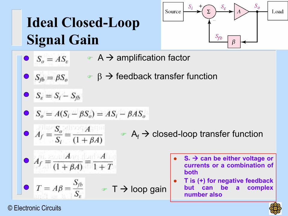
Ideal Closed-Loop
Signal Gain
A amplification factor
feedback transfer function
Af closed-loop transfer function
T loop gain
S* can be either voltage or currents or a combination of both
T is (+) for negative feedback but can be a complex number also

1-11
© Electronic Circuits
Ideal Closed-Loop
Signal Gain
If the loop gain is large so that A >> 1, the overall gain of
the feedback is a function of the feedback network only
For a large loop gain
1-12
© Electronic Circuits
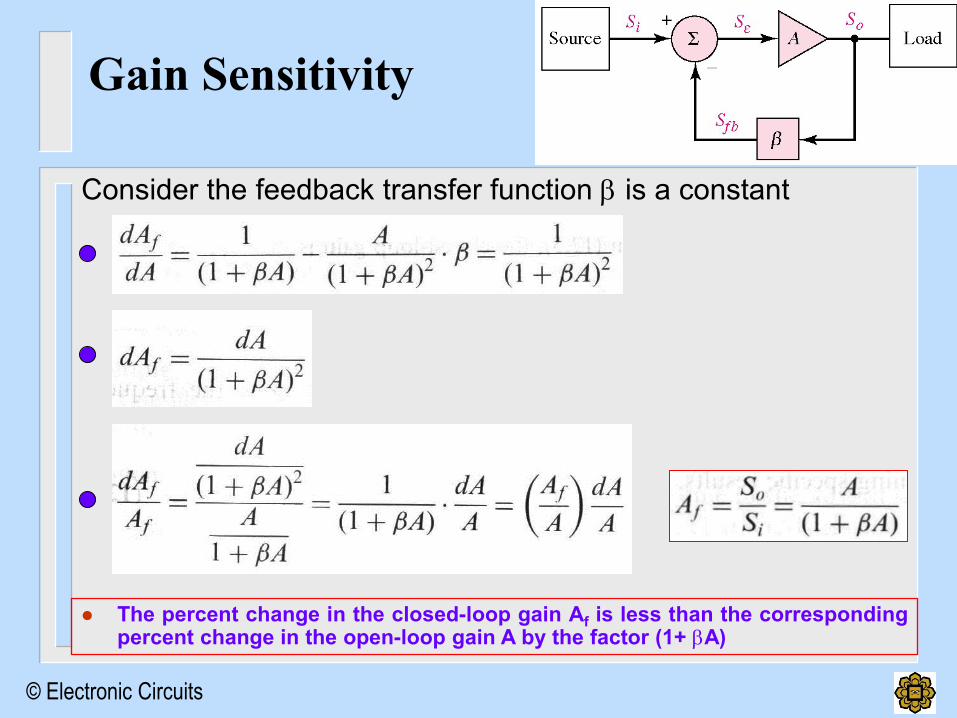
Gain Sensitivity
Consider the feedback transfer function is a constant
The percent change in the closed-loop gain Af is less than the corresponding percent change in the open-loop gain A by the factor (1+ A)

Ideal Feedback Topologies
1-14
© Electronic Circuits
Preview
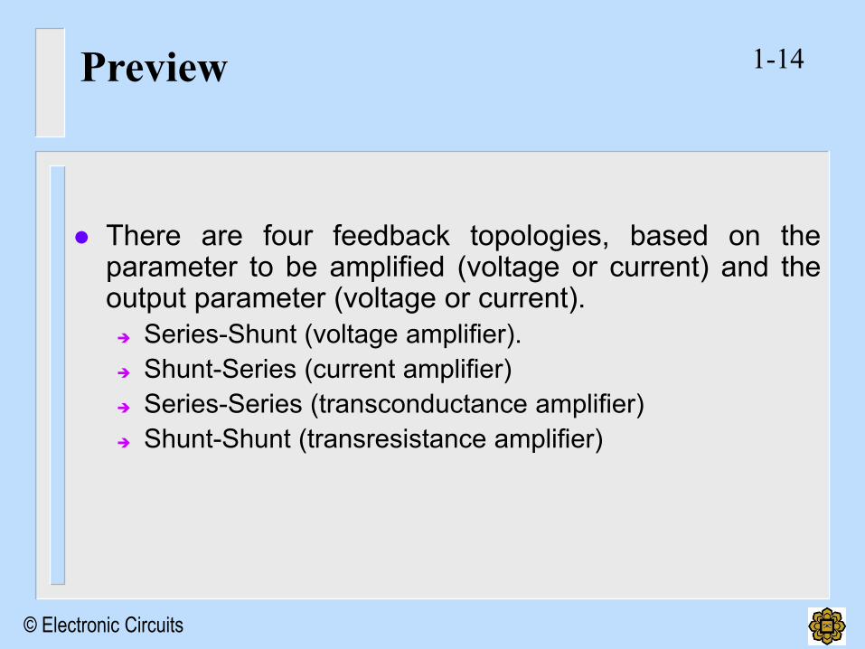
There are four feedback topologies, based on the parameter to be amplified (voltage or current) and the output parameter (voltage or current).
Series-Shunt (voltage amplifier).
Shunt-Series (current amplifier)
Series-Series (transconductance amplifier)
Shunt-Shunt (transresistance amplifier)

1-15
© Electronic Circuits
Preview

1-16
© Electronic Circuits
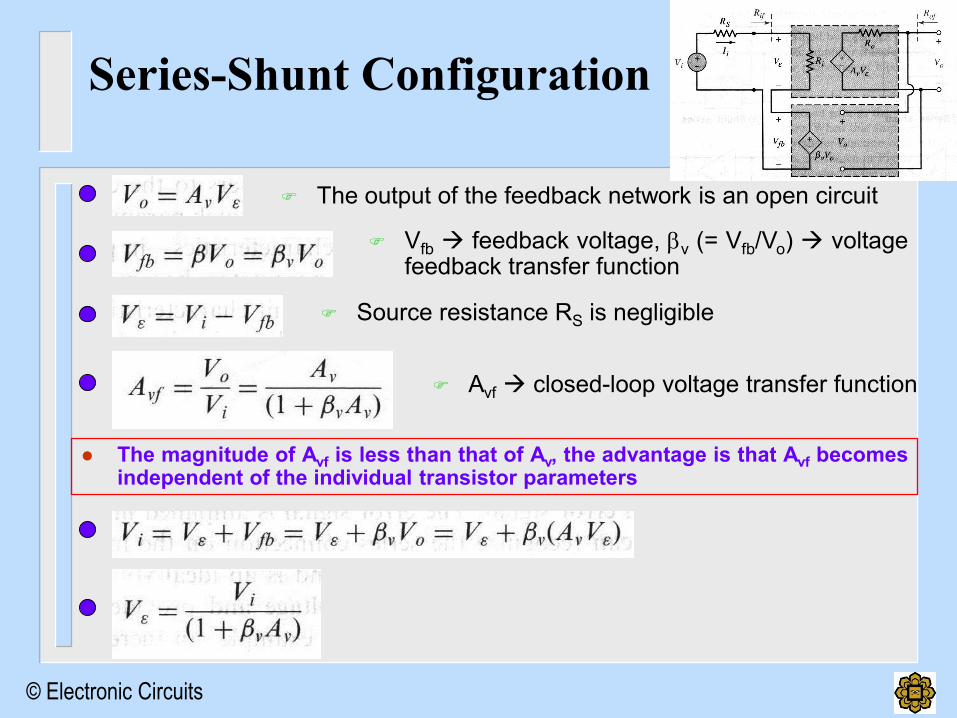
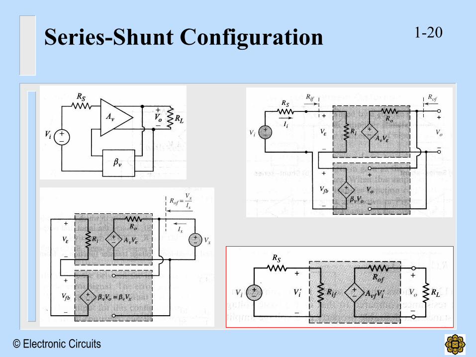
Series-Shunt Configuration
The circuit is a voltage-controlled voltage source and is an ideal voltage amplifier.
The feedback circuit samples the output voltage and provides a feedback voltage in series with the source voltage.
An increase in the output voltage produces an increase in the feedback voltage, which in turn decreases the error voltage due to the negative feedback.
The smaller error voltage is amplified producing a smaller output voltage.
Which means that the output signal tends to be stabilized.
1-17
© Electronic Circuits
Series-Shunt Configuration
The output of the feedback network is an open circuit
Vfb feedback voltage, v (= Vfb/Vo) voltage feedback transfer function
Source resistance RS is negligible
Avf closed-loop voltage transfer function
The magnitude of Avf is less than that of Av, the advantage is that Avf becomes independent of the individual transistor parameters

1-18
© Electronic Circuits
Series-Shunt Configuration
A series input connection results in an increased input resistance compared to that of the basic voltage amplifier. This eliminates loading effects on the input signal source due to the amplifier
1-19
© Electronic Circuits
Series-Shunt Configuration
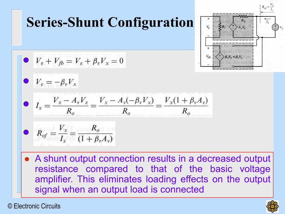
A shunt output connection results in a decreased output resistance compared to that of the basic voltage amplifier. This eliminates loading effects on the output signal when an output load is connected
1-20
© Electronic Circuits
Series-Shunt Configuration

1-21
© Electronic Circuits
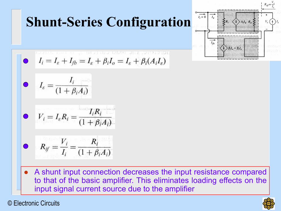
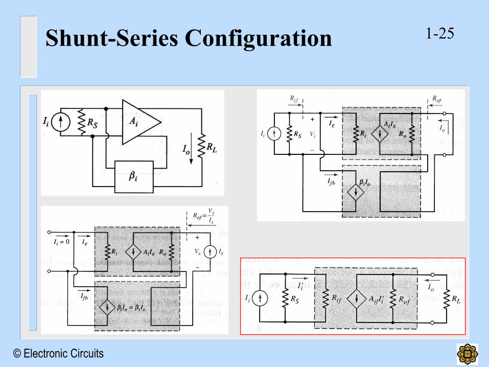
Shunt-Series Configuration
The circuit is a current-controlled current source and is an ideal current amplifier.
The feedback circuit samples the output current and provides a feedback signal in shunt with the signal current.
An increase in the output current produces an increase in the feedback current, which in turn decreases the error current due to the negative feedback.
The smaller error current is amplified producing a smaller output current.
Which means that the output signal tends to be stabilized.

1-22
© Electronic Circuits
Shunt-Series Configuration
The output of the feedback network is a short circuit
Ifb feedback current, i (= Ifb/Io) feedback current transfer function
Source resistance RS is large
Aif closed-loop current transfer function
The magnitude of Aif is less than that of Ai, the advantage is that Aif becomes independent of the individual transistor parameters
1-23
© Electronic Circuits
Shunt-Series Configuration
A shunt input connection decreases the input resistance compared to that of the basic amplifier. This eliminates loading effects on the input signal current source due to the amplifier

1-24
© Electronic Circuits
Shunt-Series Configuration
A series output connection increases the output resistance compared to that of the basic voltage amplifier. This eliminates loading effects on the output signal when an output load is connected
1-25
© Electronic Circuits
Shunt-Series Configuration
1-26
© Electronic Circuits
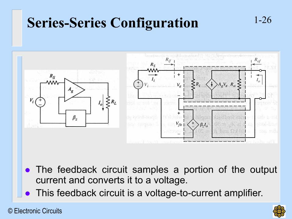
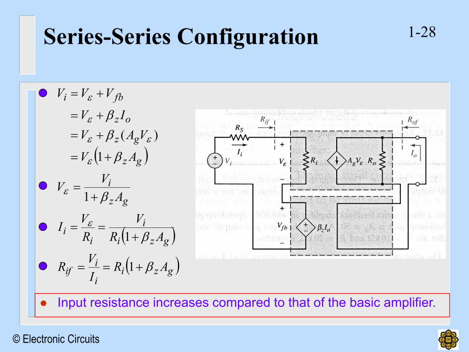
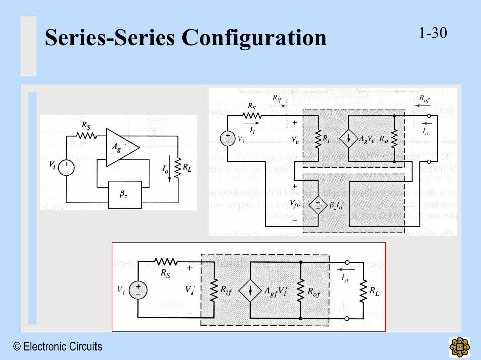
Series-Series Configuration
The feedback circuit samples a portion of the output current and converts it to a voltage.
This feedback circuit is a voltage-to-current amplifier.

1-27
© Electronic Circuits
Series-Series Configuration
The output of the feedback network is a short circuit
Vfb feedback voltage, z (= Vfb/Io) resistance feedback transfer function
Neglecting the affect of Source resistance RS
Agf closed-loop current-to-voltage transfer function or transconductance gain
1-28
© Electronic Circuits
Series-Series Configuration
Input resistance increases compared to that of the basic amplifier.
gzii
iif
gzi
i
ii
gz
i
gz
gz
oz
fbi
ARI
VR
AR
V
R
VI
A
VV
AV
VAV
IV
VVV
1
1
1
1
)(
1-29
© Electronic Circuits
Series-Series Configuration
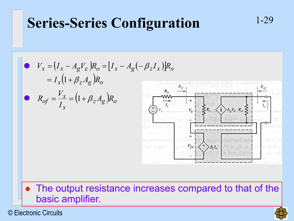
The output resistance increases compared to that of the basic amplifier.
ogzx
xof
ogzx
oxzgxogxx
RAI
VR
RAI
RIAIRVAIV
1
1
1-30
© Electronic Circuits
Series-Series Configuration

1-31
© Electronic Circuits
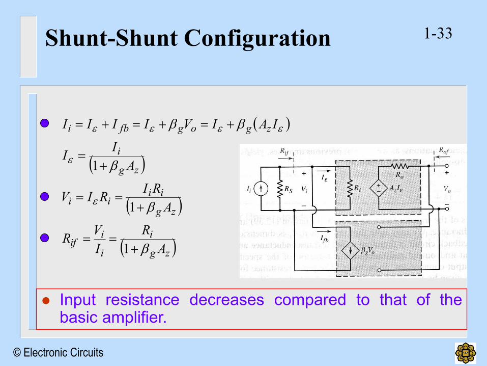
Shunt-Shunt Configuration
The feedback circuit samples a portion of the output voltage and converts it to a current.
This feedback circuit is a current-to-voltage amplifier.

1-32
© Electronic Circuits
Shunt-Shunt Configuration
The output of the feedback network is an open circuit
Ifb feedback current, g (= Ifb/Vo) conductance feedback transfer function
Source resistance RS is very large
Azf closed-loop voltage-to-current transfer function or transresistance gain
1-33
© Electronic Circuits
Shunt-Shunt Configuration
Input resistance decreases compared to that of the basic amplifier.
zg
i
i
iif
zg
iiii
zg
i
zgogfbi
A
R
I
VR
A
RIRIV
A
II
IAIVIIII
1
1
1

1-34
© Electronic Circuits
Shunt-Shunt Configuration
The output resistance decreases compared to that of the basic amplifier.
zg
o
x
xof
o
zgx
o
xgzx
o
zxx
A
R
I
VR
R
AV
R
VAV
R
IAVI
1
1

1-35
© Electronic Circuits
Shunt-Shunt Configuration

Feedback Networks
1-37
© Electronic Circuits
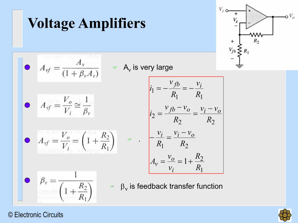
Voltage Amplifiers
1
2
21
222
111
1R
R
v
vA
R
vv
R
v
R
vv
R
vvi
R
v
R
vi
i
ov
oii
oiofb
ifb
Av is very large
v is feedback transfer function
.
1-38
© Electronic Circuits
Voltage Amplifiers
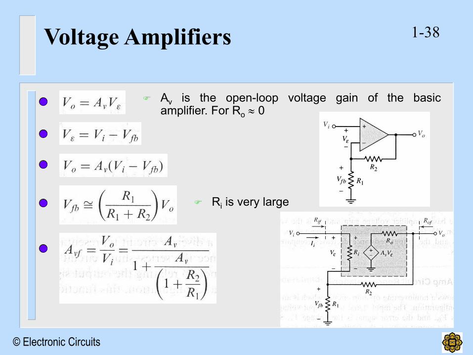
Av is the open-loop voltage gain of the basic amplifier. For Ro 0
Ri is very large
1-39
© Electronic Circuits
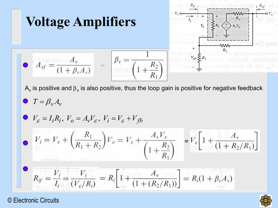
Voltage Amplifiers
.
=
vvAT
Av is positive and v is also positive, thus the loop gain is positive for negative feedback
fbivoii VVVVAVRIV ,,

1-40
© Electronic Circuits
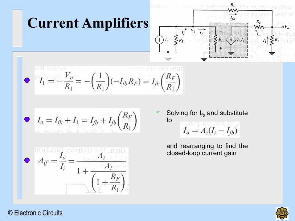
Current Amplifiers
Ai is open-loop current gain and very large
if RS >> Rif, then Ii’ Ii and I is negligible,
Assuming V1 is at virtual ground

1-41
© Electronic Circuits
Current Amplifiers
Ai is very large
Assuming V1 is at virtual ground
1-42
© Electronic Circuits
Solving for Ifb and substitute to
and rearranging to find the closed-loop current gain
Current Amplifiers
.
1-43
© Electronic Circuits
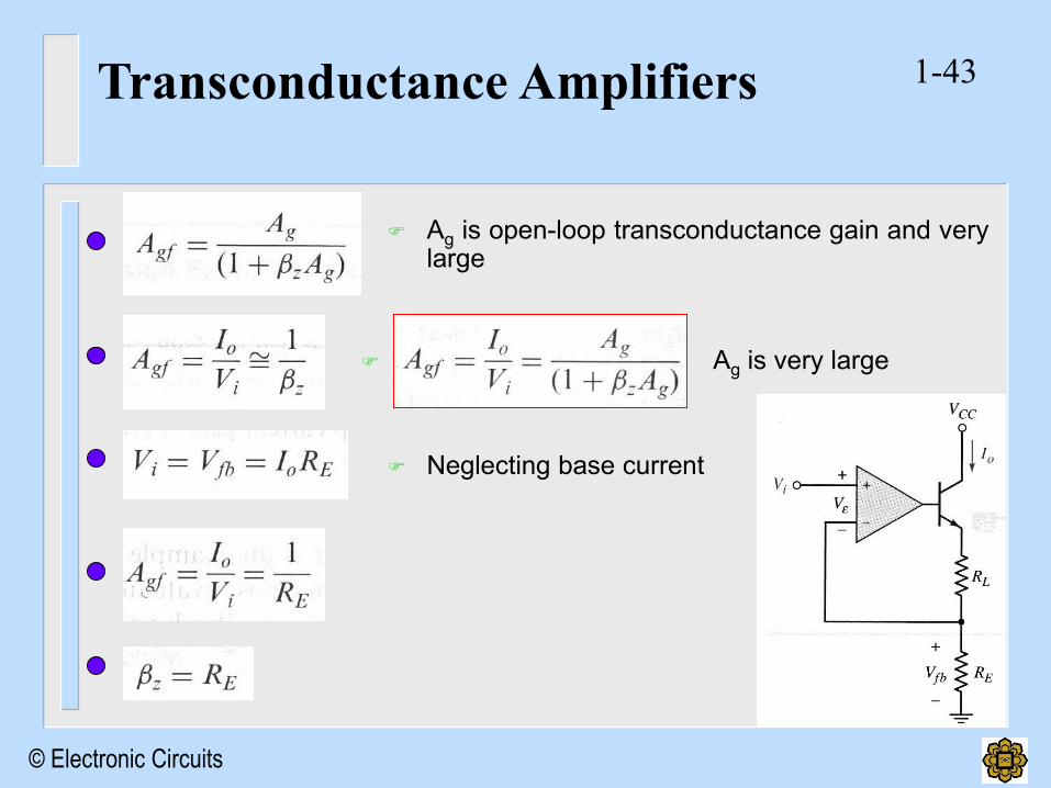
Transconductance Amplifiers
Ag is open-loop transconductance gain and very large
Neglecting base current
Ag is very large
1-44
© Electronic Circuits
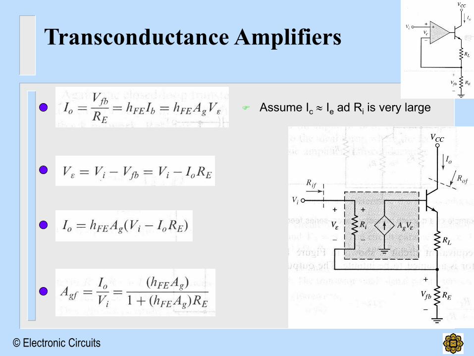
Transconductance Amplifiers
Assume Ic Ie ad Ri is very large
1-45
© Electronic Circuits
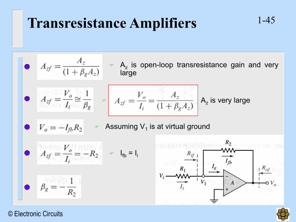
Transresistance Amplifiers
Az is open-loop transresistance gain and very large
Az is very large
Assuming V1 is at virtual ground
Ifb = Ii
1-46
© Electronic Circuits
Transresistance Amplifiers
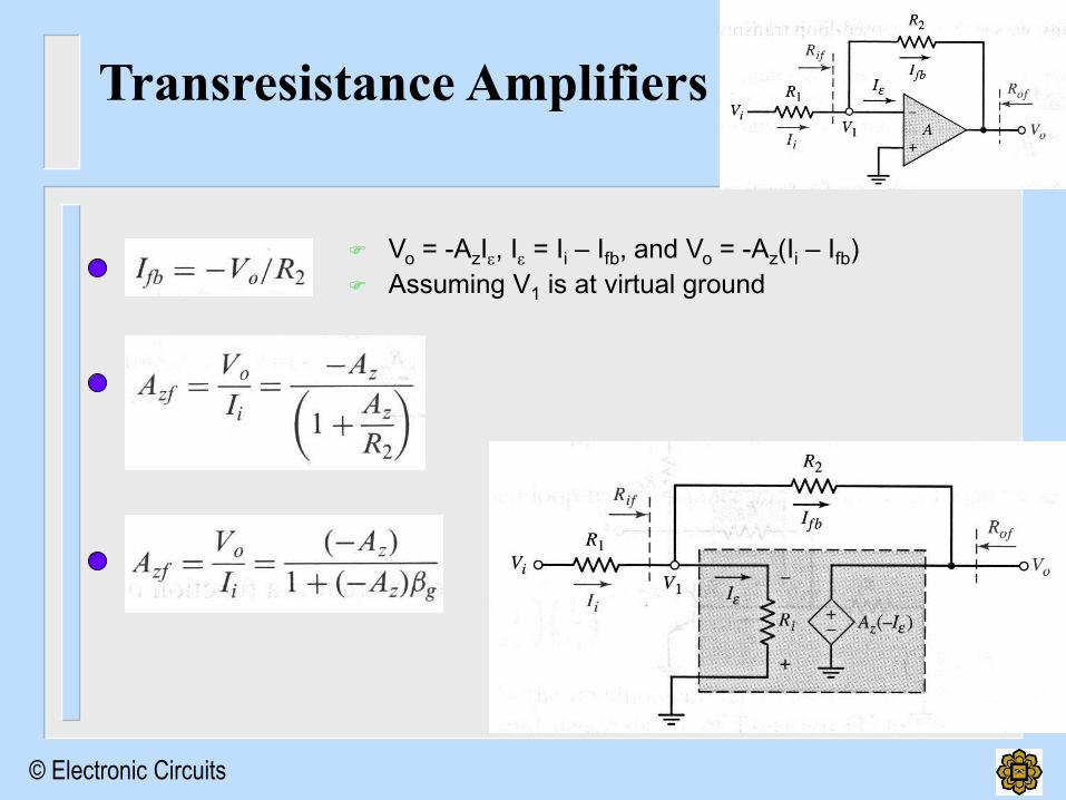
Vo = -AzI, I = Ii – Ifb, and Vo = -Az(Ii – Ifb)
Assuming V1 is at virtual ground