eas 180 mj - 400 v - internally clamped igbt · eas 180 mj - 400 v - internally clamped igbt...
TRANSCRIPT
May 2008 Rev 3 1/18
18
STGB18N40LZSTGD18N40LZ
EAS 180 mJ - 400 V - internally clamped IGBT
Features AEC Q101 compliant
180 mJ of avalanche energy @ TC = 150 °C, L = 3 mH
ESD gate-emitter protection
Gate-collector high voltage clamping
Logic level gate drive
Low saturation voltage
High pulsed current capability
Gate and gate-emitter resistor
Application Pencil coil electronic ignition driver
DescriptionThis IGBT utilizes the advanced PowerMESH™ process resulting in an excellent trade-off between switching performance and low on-state behavior.
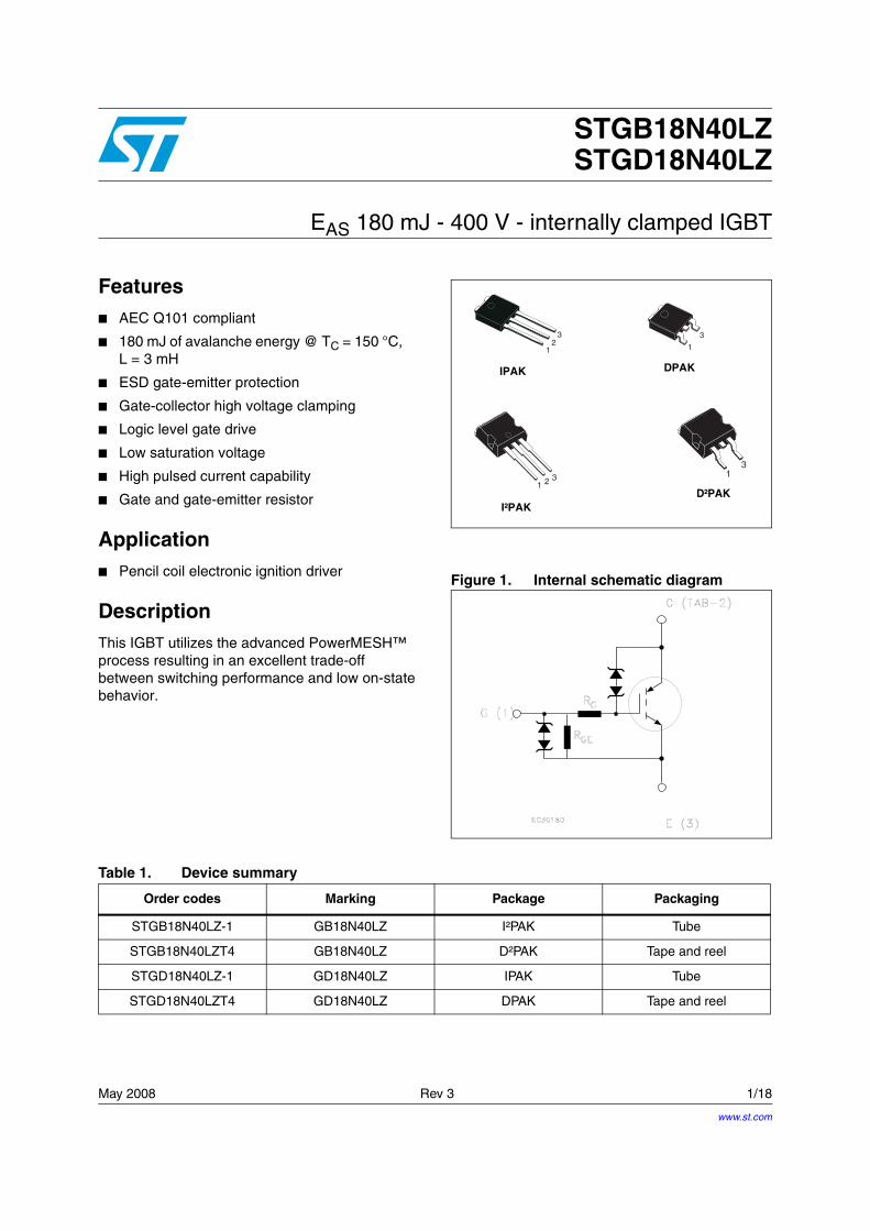
Figure 1. Internal schematic diagram
32
1 1
3
IPAK DPAK
1 2 3 13
I²PAKD²PAK
Table 1. Device summary
Order codes Marking Package Packaging
STGB18N40LZ-1 GB18N40LZ I²PAK Tube
STGB18N40LZT4 GB18N40LZ D²PAK Tape and reel
STGD18N40LZ-1 GD18N40LZ IPAK Tube
STGD18N40LZT4 GD18N40LZ DPAK Tape and reel
www.st.com

Contents STGD18N40LZ - STGB18N40LZ
2/18
Contents
1 Electrical ratings . . . . . . . . . . . . . . . . . . . . . . . . . . . . . . . . . . . . . . . . . . . . 3
2 Electrical characteristics . . . . . . . . . . . . . . . . . . . . . . . . . . . . . . . . . . . . . 4
2.1 Electrical characteristics (curves) . . . . . . . . . . . . . . . . . . . . . . . . . . . . 6
3 Test circuits . . . . . . . . . . . . . . . . . . . . . . . . . . . . . . . . . . . . . . . . . . . . . . . 9
4 Package mechanical data . . . . . . . . . . . . . . . . . . . . . . . . . . . . . . . . . . . . 10
5 Packaging mechanical data . . . . . . . . . . . . . . . . . . . . . . . . . . . . . . . . . . 13
6 Revision history . . . . . . . . . . . . . . . . . . . . . . . . . . . . . . . . . . . . . . . . . . . 14

STGD18N40LZ - STGB18N40LZ Electrical ratings
3/18
1 Electrical ratings
Table 2. Absolute maximum ratings
Symbol Parameter
Value
UnitDPAK
IPAK
D²PAK
I²PAK
VCES Collector-emitter voltage (vGE = 0) VCES(clamped) V
VECS Emitter collector voltage (VGE = 0) 20 V
IC (1)
1. Calculated according to the iterative formula:
Collector current (continuous) at TC = 100 °C 25 30 A
ICP (2)
2. Pulse width limited by max. junction temperature allowed
Pulsed collector current 40 A
VGE Gate-emitter voltage VGE(clamped) V
PTOT Total dissipation at TC = 25 °C 125 150 W
EAS Single pulse energy TC= 25 °C, L = 3 mH, RG = 1 KΩ 300 mJ
EAS Single pulse energy TC=150 °C, L = 3 mH, RG = 1 KΩ 180 mJ
ESD
Human body model, R= 1550 Ω, C = 100 pF 8 kV
Machine model, R = 0, C = 100 pF 800 V
Charged device model 2 kV
Tstg Storage temperature– 55 to 175 °C
Tj Operating junction temperature
Table 3. Thermal resistance
Symbol Parameter
Value
UnitDPAK
IPAK
D²PAK
I²PAK
Rthj-case Thermal resistance junction-case max 1.2 1 °C/W
Rthj-amb Thermal resistance junction-ambient max 65 62.5 °C/W
IC TC( )TJMAX TC–
RTHJ C– VCESAT MAX( ) TC IC,( )×------------------------------------------------------------------------------------------------------=

Electrical characteristics STGD18N40LZ - STGB18N40LZ
4/18
2 Electrical characteristics
(TCASE=25°C unless otherwise specified)
Table 4. Static electrical characteristics
Symbol Parameter Test conditions Min. Typ. Max. Unit
VCES(clamped)
Collector emitter clamped voltage
(VGE = 0)
IC = 2 mA, RG = 1 kΩTC = - 40 °C to 150 °C
370 400 430 V
V(BR)ECS
Emitter collector break-down voltage
(VGE = 0)IC = 75 mA 20 28 V
VGE(clamped)Gate emitter clamped voltage
IG = ±2 mA 12 16 V
ICES
Collector cut-off current(VGE = 0)
VCE = 15 V, TC = 150 °C 10 µA
VCE = 200 V,TC = 150 °C 100 µA
IGESGate cut-offcurrent (VCE = 0)
VGE = ±10 V 450 625 830 µA
RGEGate emitter resistance
12 16 22 KΩ
RG Gate resistance 1.6 KΩ
VGE(th)Gate threshold voltage
VCE = 12 V, IC = 1 mA,TC = -40 °C 1.4 V
VCE = 12 V, IC = 1 mA 1.2 1.6 2.3 V
VCE = 12 V, IC = 1 mA, TC =150 °C 0.7 V
VGEPGate emitter plateau voltage
VCE = 12 V, IC = 10 A 2.9 V
VCE(sat)Collector emitter saturation voltage
VGE = 4.5 V, IC = 10 A 1.35 1.7 V
VGE = 4.5 V, IC = 10 A, TC = 150 °C
1.30 V
VGE = 3.8 V, IC = 6 A 1.30 V

STGD18N40LZ - STGB18N40LZ Electrical characteristics
5/18
Table 5. Dynamic electrical characteristics
Symbol Parameter Test conditions Min. Typ. Max. Unit
Cies Input capacitanceVCE = 25 V, f = 1 MHz,
VGE = 0
490 pF
Coes Output capacitance 90 pF
Cres Reverse transfer capacitance 6.5 pF
Qg Gate chargeVCE = 280 V, IC = 10 A,
VGE = 5 V23 nC
Table 6. Switching on/off
Symbol Parameter Test conditions Min. Typ. Max. Unit
td(on)
tr
Resistive loadTurn-on delay time Rise time
VCC = 14 V, IC = 10 A
RG = 1 kΩ, VGE = 5 V1
5.8µsµs
td(on)
tr
Resistive loadTurn-on delay timeRise time
VCC = 14 V, IC = 10 A
RG = 1 kΩ, VGE = 5 V, TC = 150 °C
15.9
µsµs
td(off)
tfdv/dt
Inductive loadTurn-off delay time
Fall time
Turn-off voltage slope
VCC = 300 V, L = 1 mH
RG = 1 kΩ, VGE = 5 V
14
6.7
90
µs
µs
V/µs
td(off)
tfdv/dt
Inductive loadTurn-off delay time Fall time
Turn-off voltage slope
VCC = 300 V, L = 1 mH
RG = 1 kΩ, VGE = 5 V
TC = 150 °C
159.8
80
µsµs
V/µs

Electrical characteristics STGD18N40LZ - STGB18N40LZ
6/18
2.1 Electrical characteristics (curves) Figure 2. Collector-emitter voltage vs
temperatureFigure 3. Collector-emitter voltage vs
temperature
Figure 4. Collector-emitter voltage vs temperature
Figure 5. Self clamped inductive switch
Figure 6. Collector current vs collector emitter voltage @ 25 °C
Figure 7. Collector current vs collector emitter voltage @ -40 °C
0
10
20
30
40
50
60
TC = 25 °C
VGE = 3 .8 V
VGE = 4 V
VGE = 4.5 VVGE = 8 V
VGE = 5 V →
VCE (V)
IC (A)HV42380
0 1 2 3 4 50
10
20
30
40
50
60
0 1 2 3 4 5 6
TC = -40 °C
VGE = 3.8 V
VGE = 4 V
VGE = 4.5 VVGE = 8 V
VGE = 5 V
VCE (V)
IC (A)HV42390

STGD18N40LZ - STGB18N40LZ Electrical characteristics
7/18
Figure 8. Collector current vs collector emitter voltage @ 175 °C
Figure 9. Transfer characteristics
Figure 10. Collector emitter leakage current vs. temperature
Figure 11. Normalized collector emitter breakdown voltage vs temperature
Figure 12. Normalized gate threshold voltage vs temperature
Figure 13. Normalized collector emitter voltage vs temperature
0
10
20
30
40
50
60
0 1 2 3 4 5 6
TC = 175 °C
VGE = 3.8 V
VGE = 4 V
VGE = 4.5 V
VGE = 8 V VGE = 5 V
VCE (V)
IC (A)HV42400
0
5
10
15
20
25
30
35
40
1.0 1.5 2.0 2.5 3.0 3.5 4.0 4.5 5.0VGE (V)
IC (A)
VCE= 5V
25°C-40°C
175°C
0
5
10
15
20
25
30
35
40
1.0 1.5 2.0 2.5 3.0 3.5 4.0 4.5 5.0VGE (V)
IC (A)
VCE= 5V
25°C-40°C
175°C
HV38710
Electrical characteristics STGD18N40LZ - STGB18N40LZ
8/18
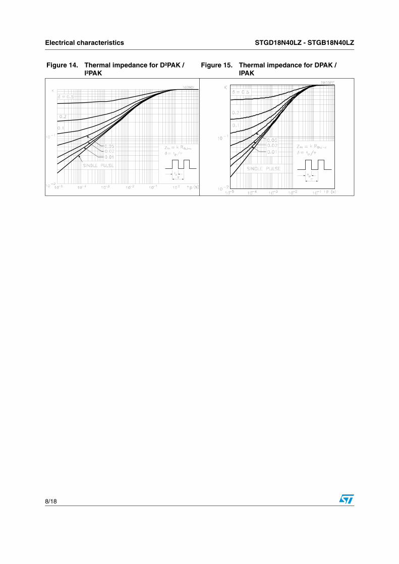
Figure 14. Thermal impedance for D²PAK / I²PAK
Figure 15. Thermal impedance for DPAK / IPAK
STGD18N40LZ - STGB18N40LZ Test circuits
9/18
3 Test circuits
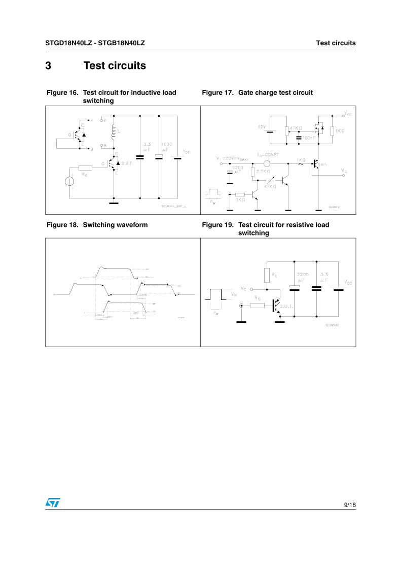
Figure 16. Test circuit for inductive load switching
Figure 17. Gate charge test circuit
Figure 18. Switching waveform Figure 19. Test circuit for resistive load switching
Package mechanical data STGD18N40LZ - STGB18N40LZ
10/18
4 Package mechanical data
In order to meet environmental requirements, ST offers these devices in ECOPACK® packages. These packages have a lead-free second level interconnect. The category of second level interconnect is marked on the package and on the inner box label, in compliance with JEDEC Standard JESD97. The maximum ratings related to soldering conditions are also marked on the inner box label. ECOPACK is an ST trademark. ECOPACK specifications are available at: www.st.com

STGD18N40LZ - STGB18N40LZ Package mechanical data
11/18
DIM.mm.
min. typ max.
A 2.20 2.40
A1 0.90 1.10
A2 0.03 0.23
b 0.64 0.90
b4 5.20 5.40
c 0.45 0.60
c2 0.48 0.60
D 6.00 6.20
D1 5.10
E 6.40 6.60
E1 4.70
e 2.28
e1 4.40 4.60
H 9.35 10.10
L 1
L1 2.80
L2 0.80
L4 0.60 1
R 0.20
V2 0 o 8 o
TO-252 (DPAK) mechanical data
0068772_G

Package mechanical data STGD18N40LZ - STGB18N40LZ
12/18
DIM.mm.
min. typ max.
A 2.20 2.40
A1 0.90 1.10
b 0.64 0.90
b2 0.95
b4 5.20 5.40
c 0.45 0.60
c2 0.48 0.60
D 6.00 6.20
E 6.40 6.60
e 2.28
e1 4.40 4.60
H 16.10
L 9.00 9.40
(L1) 0.80 1.20
L2 0.80
V1 10 o
TO-251 (IPAK) mechanical data
0068771_H
STGD18N40LZ - STGB18N40LZ Package mechanical data
13/18
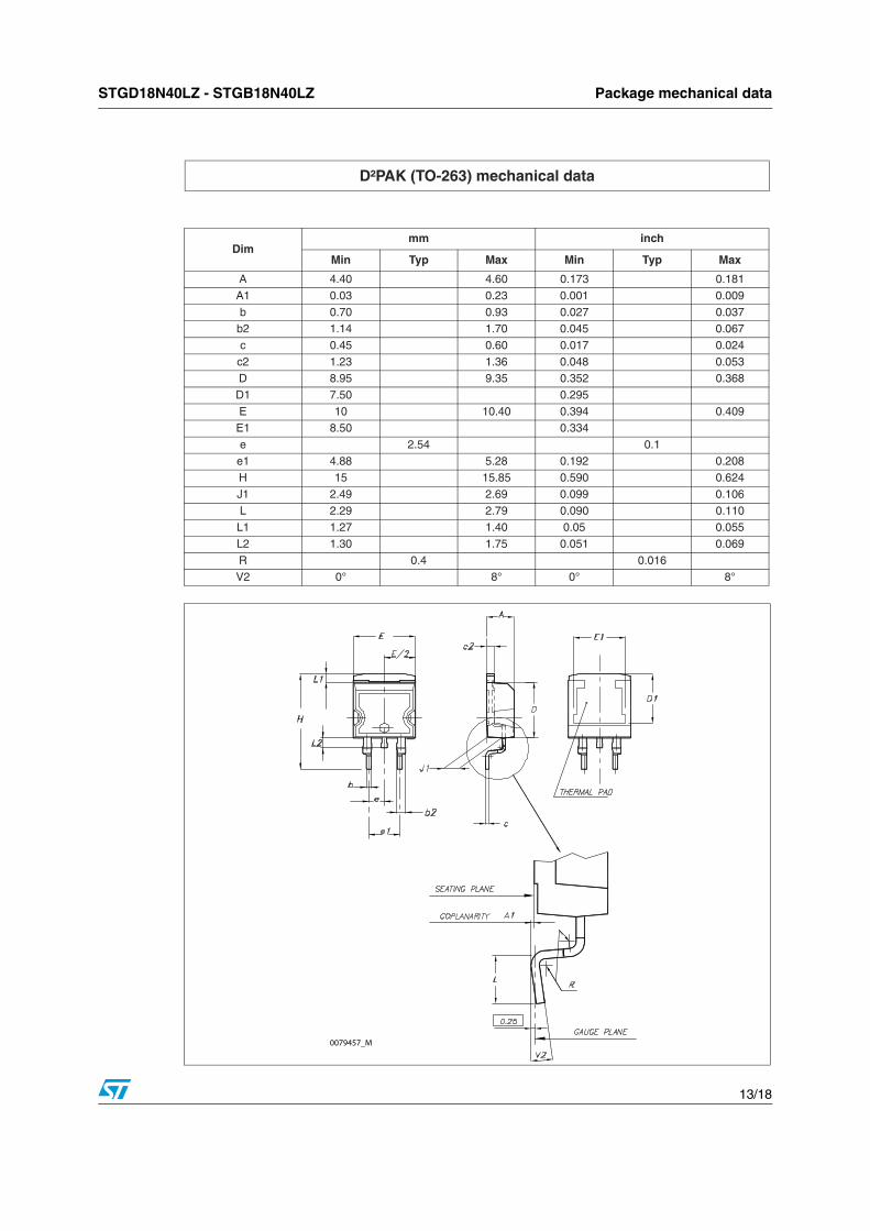
D²PAK (TO-263) mechanical data
Dimmm inch
Min Typ Max Min Typ Max
A 4.40 4.60 0.173 0.181
A1 0.03 0.23 0.001 0.009
b 0.70 0.93 0.027 0.037b2 1.14 1.70 0.045 0.067
c 0.45 0.60 0.017 0.024
c2 1.23 1.36 0.048 0.053D 8.95 9.35 0.352 0.368
D1 7.50 0.295
E 10 10.40 0.394 0.409E1 8.50 0.334
e 2.54 0.1
e1 4.88 5.28 0.192 0.208H 15 15.85 0.590 0.624
J1 2.49 2.69 0.099 0.106
L 2.29 2.79 0.090 0.110L1 1.27 1.40 0.05 0.055
L2 1.30 1.75 0.051 0.069
R 0.4 0.016V2 0° 8° 0° 8°
0079457_M

Package mechanical data STGD18N40LZ - STGB18N40LZ
14/18
I²PAK (TO-262) mechanical data
Dimmm inch
Min Typ Max Min Typ Max
A 4.40 4.60 0.173 0.181
A1 2.40 2.72 0.094 0.107
b 0.61 0.88 0.024 0.034b1 1.14 1.70 0.044 0.066
c 0.49 0.70 0.019 0.027
c2 1.23 1.32 0.048 0.052D 8.95 9.35 0.352 0.368
e 2.40 2.70 0.094 0.106
e1 4.95 5.15 0.194 0.202E 10 10.40 0.393 0.410
L 13 14 0.511 0.551
L1 3.50 3.93 0.137 0.154L2 1.27 1.40 0.050 0.055
STGD18N40LZ - STGB18N40LZ Packaging mechanical data
15/18
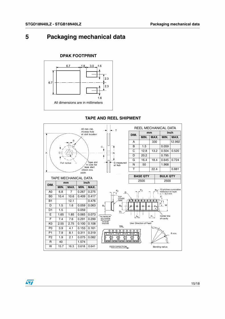
5 Packaging mechanical data
TAPE AND REEL SHIPMENT
DPAK FOOTPRINT
DIM.mm inch
MIN. MAX. MIN. MAX.
A 330 12.992
B 1.5 0.059
C 12.8 13.2 0.504 0.520
D 20.2 0.795
G 16.4 18.4 0.645 0.724
N 50 1.968
T 22.4 0.881
BASE QTY BULK QTY
2500 2500
REEL MECHANICAL DATA
DIM.mm inch
MIN. MAX. MIN. MAX.
A0 6.8 7 0.267 0.275
B0 10.4 10.6 0.409 0.417
B1 12.1 0.476
D 1.5 1.6 0.059 0.063
D1 1.5 0.059
E 1.65 1.85 0.065 0.073
F 7.4 7.6 0.291 0.299
K0 2.55 2.75 0.100 0.108
P0 3.9 4.1 0.153 0.161
P1 7.9 8.1 0.311 0.319
P2 1.9 2.1 0.075 0.082
R 40 1.574
W 15.7 16.3 0.618 0.641
TAPE MECHANICAL DATA
All dimensions are in millimeters
Packaging mechanical data STGD18N40LZ - STGB18N40LZ
16/18
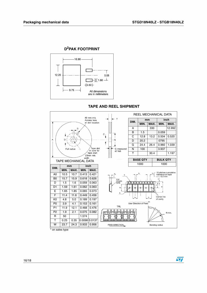
TAPE AND REEL SHIPMENT
D2PAK FOOTPRINT
* on sales type
DIM.mm inch
MIN. MAX. MIN. MAX.
A 330 12.992
B 1.5 0.059
C 12.8 13.2 0.504 0.520
D 20.2 0795
G 24.4 26.4 0.960 1.039
N 100 3.937
T 30.4 1.197
BASE QTY BULK QTY
1000 1000
REEL MECHANICAL DATA
DIM.mm inch
MIN. MAX. MIN. MAX.
A0 10.5 10.7 0.413 0.421
B0 15.7 15.9 0.618 0.626
D 1.5 1.6 0.059 0.063
D1 1.59 1.61 0.062 0.063
E 1.65 1.85 0.065 0.073
F 11.4 11.6 0.449 0.456
K0 4.8 5.0 0.189 0.197
P0 3.9 4.1 0.153 0.161
P1 11.9 12.1 0.468 0.476
P2 1.9 2.1 0.075 0.082
R 50 1.574
T 0.25 0.35 0.0098 0.0137
W 23.7 24.3 0.933 0.956
TAPE MECHANICAL DATA
STGD18N40LZ - STGB18N40LZ Revision history
17/18
6 Revision history
Table 7. Document revision history
Date Revision Changes
18-Jan-2008 1 Initial release.
07-Mar-2008 2 Modified Figure 7, Figure 8, Figure 10.
07-May-2008 3 Modified Figure 9
STGD18N40LZ - STGB18N40LZ
18/18
Please Read Carefully:
Information in this document is provided solely in connection with ST products. STMicroelectronics NV and its subsidiaries (“ST”) reserve theright to make changes, corrections, modifications or improvements, to this document, and the products and services described herein at anytime, without notice.
All ST products are sold pursuant to ST’s terms and conditions of sale.
Purchasers are solely responsible for the choice, selection and use of the ST products and services described herein, and ST assumes noliability whatsoever relating to the choice, selection or use of the ST products and services described herein.
No license, express or implied, by estoppel or otherwise, to any intellectual property rights is granted under this document. If any part of thisdocument refers to any third party products or services it shall not be deemed a license grant by ST for the use of such third party productsor services, or any intellectual property contained therein or considered as a warranty covering the use in any manner whatsoever of suchthird party products or services or any intellectual property contained therein.
UNLESS OTHERWISE SET FORTH IN ST’S TERMS AND CONDITIONS OF SALE ST DISCLAIMS ANY EXPRESS OR IMPLIEDWARRANTY WITH RESPECT TO THE USE AND/OR SALE OF ST PRODUCTS INCLUDING WITHOUT LIMITATION IMPLIEDWARRANTIES OF MERCHANTABILITY, FITNESS FOR A PARTICULAR PURPOSE (AND THEIR EQUIVALENTS UNDER THE LAWSOF ANY JURISDICTION), OR INFRINGEMENT OF ANY PATENT, COPYRIGHT OR OTHER INTELLECTUAL PROPERTY RIGHT.
UNLESS EXPRESSLY APPROVED IN WRITING BY AN AUTHORIZED ST REPRESENTATIVE, ST PRODUCTS ARE NOTRECOMMENDED, AUTHORIZED OR WARRANTED FOR USE IN MILITARY, AIR CRAFT, SPACE, LIFE SAVING, OR LIFE SUSTAININGAPPLICATIONS, NOR IN PRODUCTS OR SYSTEMS WHERE FAILURE OR MALFUNCTION MAY RESULT IN PERSONAL INJURY,DEATH, OR SEVERE PROPERTY OR ENVIRONMENTAL DAMAGE. ST PRODUCTS WHICH ARE NOT SPECIFIED AS "AUTOMOTIVEGRADE" MAY ONLY BE USED IN AUTOMOTIVE APPLICATIONS AT USER’S OWN RISK.
Resale of ST products with provisions different from the statements and/or technical features set forth in this document shall immediately voidany warranty granted by ST for the ST product or service described herein and shall not create or extend in any manner whatsoever, anyliability of ST.
ST and the ST logo are trademarks or registered trademarks of ST in various countries.
Information in this document supersedes and replaces all information previously supplied.
The ST logo is a registered trademark of STMicroelectronics. All other names are the property of their respective owners.
© 2008 STMicroelectronics - All rights reserved
STMicroelectronics group of companies
Australia - Belgium - Brazil - Canada - China - Czech Republic - Finland - France - Germany - Hong Kong - India - Israel - Italy - Japan - Malaysia - Malta - Morocco - Singapore - Spain - Sweden - Switzerland - United Kingdom - United States of America
www.st.com