e195304.pdf
TRANSCRIPT
PHYSICAL REVIEW B 83, 195304 (2011)
Assessment of approximations in nonequilibrium Green’s function theory
T. Kubis*
Network for Computational Nanotechnology, Birk Nanotechnology Center, School of Electrical and Computer Engineering,Purdue University, West Lafayette, Indiana 47907, USA
P. VoglWalter Schottky Institute, Technische Universitat Munchen, Am Coulombwall 3, D-85748 Garching, Germany
(Received 3 February 2011; published 5 May 2011)
A nonequilibrium Green’s function (NEGF) method for stationary carrier dynamics in open semiconductornanodevices is presented that includes all relevant incoherent scattering mechanisms. A consistent lead modelis developed that ensures all observables to reflect intrinsic device properties. By restricting the charge self-consistent calculations to vertical transport through heterostructures, the Green’s functions and self-energies canbe determined very accurately. This allows us to assess many commonly used approximations, such as ballisticleads, decoupling of Dyson’s and Keldysh’s equations, truncated or momentum-averaged self-energies, and localself-energies in the NEGF formalism in detail, and to study limiting cases such as diffusive transport in resistors.The comparison of exact and approximated NEGF calculations illustrates the physical implications and validityof common approximations and suggests numerically efficient simplifications.
DOI: 10.1103/PhysRevB.83.195304 PACS number(s): 72.10.−d, 72.20.Dp, 72.20.Ht
I. INTRODUCTION
The realistic prediction of carrier dynamics in state-of-the-art semiconductor devices requires a scheme that treats carrierinterferences, coherent tunneling, and quantum confinement aswell as energy and momentum relaxation on an equal footing.In addition to approaches based on the Pauli master equationand the density matrix formalism,1–4 the nonequilibriumGreen’s function (NEGF) method is among the most widelyemployed methods to describe carrier dynamics in openquantum systems.5,6 In fact, the NEGF method has beenapplied successfully to a great variety of systems ranging fromphonon transport,7,8 spin transport,9,10 electron11,12 dynamicsin metals,13–16 organic molecules and fullerenes,17–20 andsemiconductor nanostructures.21–23 Unfortunately, the basicNEGF equations are complex, mathematically cumbersome,and their numerical solution is extremely demanding. There-fore, a wide range of different approximations for particulardevices and situations have been developed and employed thatmake it difficult to judge their adequacy for other problems.In addition, suitable boundary conditions for current-carryingnanometer devices that account for a finite current densityin the leads have not been studied in detail in terms of thismethod yet. As a consequence, the validity of the NEGFmethod in some limiting cases such as simple resistors is stilldebatable.
In this paper, a fully self-consistent implementation of theNEGF method for open nanodevices is presented and usedto assess the most common approximations employed in thismethod’s implementation. These approximations have beendiscussed up to now only for very specific device applications.In this paper, we attempt to provide concrete and generalguidelines for advisable simplifications.
The most common approximation in NEGF calculationsis to set to zero all scattering processes altogether. This isequivalent of solving the Schrodinger or Lippmann-Schwingerequation with open boundary conditions and describes bal-listic transport. This approximation can be adequate for low
temperatures and high mobilities.24–27 Another very com-mon and numerically efficient scheme is the Buttiker-probemodel, where one replaces the individual physical scatteringmechanisms by a global energy and momentum absorbingself-energy.28–32 Once incoherent scattering is taken intoaccount, it has to be included in the total simulation domain,i.e., in the device and its surroundings, to avoid artificialinterferences at the device boundaries. This has been shownfor local scattering mechanisms, and we verify this findingalso for nonlocal scattering events.29,33 For quantum cascadestructures that consist of hundreds of quantum wells in anexternal electric field, it is common to use periodic boundaryconditions rather than treating the system as a scatteringproblem with attached asymptotic leads.34–36 This proceduresimplifies the NEGF calculations significantly as well, butis adequate only for field-periodic device structures withsufficient energy dissipation. Another common approximationis to solve only those parts of the NEGF equations thatdetermine the resonance and bound-state energies and sidestepthe calculation of the occupation numbers, i.e., the Keldyshequations.37 In some cases, this approximation has been foundto violate Pauli’s principle,37 but more detailed investigationsof this interesting ansatz have not been performed so far.Another numerically time-saving approximation that has beenused for superlattice calculations replaces the momentumdependence of the phonon- and other scattering potentialsby suitable averages.34,38,39 Finally, important insight intothe NEGF method has been obtained by comparing theresults of NEGF calculations for Wannier-Stark-type laddersystems and quantum cascade structures with semiclassi-cal Monte Carlo calculations.38,40,41 Whether these resultsalso apply to typical resistive devices n-i-n or quantum-well structures will be one of the focuses of the presentpaper.
While we analyze most of the above-mentioned approxi-mations in equilibrium, another very common approximationaffects nonequilibrium situations with a finite current density
195304-11098-0121/2011/83(19)/195304(12) ©2011 American Physical Society

T. KUBIS AND P. VOGL PHYSICAL REVIEW B 83, 195304 (2011)
in the device: It is very common to assume the leads ofopen devices to remain in equilibrium irrespective of a finitedevice current. Nevertheless, it is well known that such anapproximation generates electrostatic charges at the device-lead interfaces.27,42–44 Therefore, several models have beendeveloped to compensate these charges. In high resistivedevices, it is common to compensate transferred charges byadjusting the chemical potentials of the Fermi distributionswithin the leads. At higher device current densities, however, ithas been suggested to avoid equilibrium electron distributionswithin the leads to account for current conservation beyondthe device boundaries.42,44–46 Most of the later approachesimplement a shifted Fermi distribution for the lead electrons.Typically this shift is calculated within a drift-diffusion modelwith a given lead electron mobility.42,44,45,47,48 The natureof transport in nanoscale devices is strongly dependent onthe device details and can vary from diffusive to ballistic.Therefore, we extend in this paper the lead model of shiftedlead Fermi distributions so that a detailed knowledge of thecarrier mobility is no longer required. Instead, the shift ofthe lead electron distribution is determined such that surfacecharges at the device-lead boundaries are exactly compensated.Thus, our lead model ensures that the calculated physicalobservables, and particularly the I -V characteristics, reflectintrinsic properties of the device. It is finally shown that theNEGF method yields correct results in the limiting case ofdiffusive transport by a comparison with solutions of theBoltzmann equation.
In Sec. II A, we briefly introduce the governing equations. InSec. II B, a lead model is introduced that specifies the boundaryconditions for the electrostatic potential and the Green’s func-tions, respectively. The entire Sec. III is devoted to a carefulexamination and assessment of common approximations ofthe NEGF method. The consequences of using ballistic leadsare presented in Sec. III A. The crucial property of currentconservation is lost when self-energies are truncated, as shownin Sec. III B. While in some cases the decoupling of the Dysonand Keldysh equations leads to unphysical results, we discusssituations in Secs. III C and III D in which this approximationcan be justified. The consequences of neglecting the nonlocalnature of the Green’s functions is discussed in Sec. III Eand their momentum dependence is analyzed in Sec. III F.In Sec. III G, three different lead models are discussedand compared to one another. The capability of the NEGFmethod to reproduce results of semiclassical calculations isdemonstrated in Sec. III H. Finally, we summarize our findingsin Sec. IV.
II. METHOD
A. Fundamentals
To set up our notation and be able to assess variousapproximations, we briefly summarize the NEGF in thissection. We focus on stationary vertical transport in laterallyhomogeneous quantum-well heterostructures and considersuch a device to be in contact with two charge reservoirs atz = R and z = L, respectively. Thereby, we consider chargetransport as a scattering problem from source to drain withthe open device forming the scattering center. The electronic
structure is represented in terms of a single-band effective-mass model with an effective mass that may depend on thegrowth coordinate z as well as on the energy E in order to beable to incorporate nonparabolicity effects. The single-bandconduction-electron Hamiltonian is given by
H0 = −h2
2
d
dz
1
m∗(z,E)
d
dz+ h2k2
‖2m∗(z,E)
+ V (z),
V (z) = Ec(z) − e�(z), (1)
where k‖ is the lateral electron momentum, �(z) the electro-static potential, and Ec(z) denotes the material- and position-dependent conduction-band edge, including the band offsets.Within the NEGF formalism, stationary transport in openquantum-mechanical systems is characterized by four coupledpartial differential equations for the electronic retarded andlesser Green’s functions GR,G<, respectively.49 In operatorform, they read
GR = (E − H0 − �R)−1,
G< = GR�<GR†,
�< = G<D<,
�R = GRDR + GRD< + G<DR. (2)
Here, D is the sum of all environmental Green’s functionsthat incorporate phonons, impurities, and interface roughness,and � denotes the self-energies. The solutions of Eqs. (2) inreal space do not require one to solve an eigenvalue problem.Therefore, an energy-dependent mass in the HamiltonianH0 does not increase the complexity of the solution. AllGreen’s functions G(z,z′,k‖,) and self-energies �(z,z′,k‖,E)are taken as functions of two spatial coordinates z,z′, the lateralmomentum k‖, and the energy E. Once the Green’s functionsare known, the observables such as the spatially resolveddensity n(z) and the current density j (z) can be determinedstraightforwardly,
n(z) =∫
dEn(z,E)
= 2
(2π )3Im
∫dE
∫d�k‖G<(z,z,k‖,E), (3)
j (z) = − he
(2π )3limz′→z
∫dE
∫d�k‖
1
m∗(z,E)
×Re
(d
dz− d
dz′
)G<(z,z′,k‖,E). (4)
If not explicitly stated otherwise, we take into account inelasticacoustic and polar-optical-phonon scattering, scattering bycharged impurities, rough interfaces, and the electron-electroninteraction in the Hartree approximation. The scattering self-energies are determined in the self-consistent Born approx-imation including their full nonlocal momentum and energydependence.50 Taking into account scattering to infinite orderis a prerequisite for obeying current conservation exactly.50 Inthe real-space basis employed in this work, we exemplify thegeneral, nonlocal retarded, and lesser scattering self-energiesfor polar-optical-phonon (pop) and charged impurity (imp)
195304-2

ASSESSMENT OF APPROXIMATIONS IN . . . PHYSICAL REVIEW B 83, 195304 (2011)
scattering, respectively,37
�<pop(z,z′,k‖,E) = γπ
(2π )3
∫d�l‖ Vpop(z,z′,|�k‖ − �l‖|)[n0G
<(z,z′,l‖,E − hω0) + (1 + n0)G<(z,z′,l‖,E + hω0)], (5)
�Rpop(z,z′,k‖,E) = γπ
(2π )3
∫d�l‖ Vpop(z,z′,|�k‖ − �l‖|)
[(1 + n0)GR(z,z′,l‖,E − hω0) + n0G
R(z,z′,l‖,E + hω0)
+ 1
2G<(z,z′,l‖,E − hω0) − 1
2G<(z,z′,l‖,E + hω0) + iP
∫dE′
2π
(G<(z,z′,l‖,E′)E − E′ − hω0
− G<(z,z′,l‖,E′)E − E′ + hω0
)],
Vpop(z,z′,k‖) = e−√
k2‖+q2
D |z−z′ |√k2‖ + q2
D
(1 − q2
D|z − z′|2√
k2‖ + q2
D
− q2D
2(k2‖ + q2
D
))
, (6)
�imp(z,z′,k‖,E) = e4
16π2ε20ε
2r
∫d�q‖ Vimp(z,z′,|�k‖ − �q‖|)G(z,z′,q‖,E),Vimp(z,z′,k‖) =
∫dz′′ ND(z′′)
e−√
q2D+k2
‖ (|z−z′′ |+|z′−z′′ |)
q2D + k2
‖.
(7)
In these equations, qD denotes the inverse Debye screeninglength, ND(z) is the ionized impurity concentration, and n0
denotes the equilibrium Bose phonon number at the chosentemperature. We note that the contribution of the principalvalue integral in Eq. (6) is small in laterally homogeneousheterostructures and can be neglected.34,35 The expression for�imp holds for both the retarded and the lesser self-energyand contains the same type of Green’s function, i.e., �R
imp ∝GR,�<
imp ∝ G<. The polar-optical Frohlich coupling constantγ is given by
γ = e2 hω0
2ε0
(1
ε∞− 1
εr
), (8)
where ω0 is the constant optical-phonon frequency, and εr ,ε∞ are (device averaged values of) the static and dynamicdielectric constant, respectively.51 These two scattering self-energies reflect all important properties of self-energies thatwe will discuss in the subsequent sections.
B. Lead model for open devices
Since we focus on open quantum systems, we need toaugment the system of Eqs. (2) for the Green’s functions bysuitable boundary conditions, i.e., by a consistent treatmentof the leads. Given the fact that full NEGF calculations canonly be performed for very small nanoscale semiconductorstructures at this time, different treatments of the leads aremajor sources of discrepancy between different models. Wewill therefore present our lead model in some detail and discussthe effect of different models on observable device propertiesin the next section.
We consider open, laterally homogeneous devices withelectrons in a single parabolic conduction band and attacha semi-infinite lead to the left and to the right of the structure,respectively. Our main goal in setting up a lead model is tomake sure the physics is controlled by the interior of the devicerather than the leads. Physically, this is only possible if thecharge density near the device-lead interface is sufficientlyhigh to screen the electric fields within the device so that it is
reasonable to assume flat band boundary conditions. Given thispremise, we assume furthermore that the lead-device interfacesare sufficiently smooth not to cause significant reflections orinterference effects. We note that the present lead model canbe generalized to fully three-dimensional devices with anynumber of leads, as we show in the Appendix.
In our model, each semi-infinite lead � ∈ {L,R} is charac-terized by a constant effective mass m∗
� , position-independentelectron density n� corresponding to a chemical potential μ�,and a constant electrostatic potential ��. The bottom of theconduction band in each lead is denoted by Ec,�. To getreflectionless contacts, i.e., smooth device-lead transitions,we extend the device density of states adjacent to the leadscontinuously into the leads.
For this purpose, the device Green’s functions are calculatedincluding the contact self-energies �R
con and �<con. This requires
that we include scattering within the leads to the extent thatwe solve the retarded surface Green’s function of the lead self-consistently with �R of the device, but assume a fixed electrondistribution.52 This scheme is analogous to the one proposedin Ref. 53, but we maintain the full off-diagonal character ofthe self-energies across the lead-device interface and replacethe scalar elements of the contact self-energy algorithm inRef. 53 by matrices. The size of these matrices is given by thefinite range of the scattering self-energies in the device. Theresulting set of nonlinear equations is then solved iteratively.53
Within the device, we solve the Poisson equation
ε0d
dzεr (z)
d�(z)
dz= e[n(z) − ND(z)] (9)
self-consistently with all Green’s functions in the device. Notethat global charge neutrality of the device requires εr,L�′
L =εr,R�′
R or simply �′L = �′
R for a single material device, asfollows from integration of Eq. (9). Since we assume a highcarrier density near the contacts, we use the stronger conditions
(I)d�(z)
dz
∣∣∣∣z=R
= 0,
(10)
195304-3
T. KUBIS AND P. VOGL PHYSICAL REVIEW B 83, 195304 (2011)
(II)d�(z)
dz
∣∣∣∣z=L
= 0.
In equilibrium, i.e., for zero applied bias, we assumethe electronic distribution within the leads to be given byequilibrium Fermi distributions. Depending on the devicedetails, our electrostatic boundary conditions (I) and (II) mayresult in a finite built-in potential across the device,
Vbuilt-in = e[�L − �R]equilibrium. (11)
We assume the potential Vbuilt-in to remain the same innonequilibrium situations.
In a nonequilibrium situation, charge is transferred fromthe source to the drain side of the device. Without anycompensation, this charge transport results in a dipole atthe device boundaries: a positive charge at the source anda negative charge at the drain sided boundary of the device. Itis well known that such a dipole prohibits the applied bias todrop completely within the device.1,27,42,44,45 To compensatethis charge dipole at the device boundaries, we assume shiftedFermi distributions within the leads.1,42,44,45 Accordingly, theelectron distribution in lead � reads
f�(k‖,kD,�,E,μ�) = {exp[β(E� − μ�)] + 1}−1, (12)
with
E� = h2
2m∗�
[k2‖ + (kz,�(E) − kD,�)2]. (13)
Hereby, the sign of the variable kD,� depends on the direction ofthe electron flux through the contact. It shifts the center of thelead’s Fermi sphere parallel to the average electron momentumin the growth direction,
kz,�(E) =√
2m∗�(E − Ec� − e��)/h2 − k2
‖ . (14)
With the current flowing from source to drain, kD,� is positivein the source and negative in the drain. The shift of the Fermispheres within the leads causes charge dipoles at both leadboundaries: the source sided lead faces a positive charge at theboundary to the (metallic) reservoir and a negative charge atthe boundary with the device; The dipole of the drain sidedlead has an opposite configuration. In this way, the shift of thelead Fermi spheres allows us to move the dipole charges to thelead-reservoir interfaces and to guarantee a given bias dropwithin the device. Therefore, we iteratively determine the twoshifts kD,� of the Fermi distributions in the two leads with theNEGF results within the device until the two conditions hold,
(III) Vapplied = e[�L − �R] − Vbuilt-in = μL − μR,
(IV)
∣∣∣∣kD,L
kD,R
∣∣∣∣ = m∗LnR
m∗RnL
. (15)
Please note that these two conditions unambiguously definethe two unknown variables kD,L and kD,R . Condition (III)guarantees that only one global dipole persists, i.e., the dipolebetween source and drain reservoir. Then, the total applied biasVapplied completely drops within the device. Condition (IV), onthe other hand, mimics current conservation from the leads intothe device by assuming that the current density within lead �
is proportional to kD,�n�/m∗� .44 Expression (IV) avoids the
introduction of a mobility and is plausible for both diffusive
and ballistic situations. In weakly doped and low resistivedevices, the shift kD,� may grow to values larger than kz,� forall energies E of occupied states that would lead to artificialresults. This limit is approximately reached when kD,� equalsthe Fermi vector. We therefore restrict its values to the range|kD,�| � 3
√3π2n�. An assessment of this lead model is given
in Sec. III G.
III. RESULTS AND ASSESSMENT OF COMMONAPPROXIMATIONS
In this section, we are going to assess several commonapproximations for the self-consistent solution of the NEGFequations (2). It turns out that the Green’s function approachis quite sensitive to some simplifications but less sensitive toothers, and in most cases these findings are counterintuitive.We hope that this discussion illustrates the strengths andweaknesses of the NEGF apparatus and eventually contributesto reduced numerical effort and more robust and reliablepredictions based on this method.
A. Ballistic leads
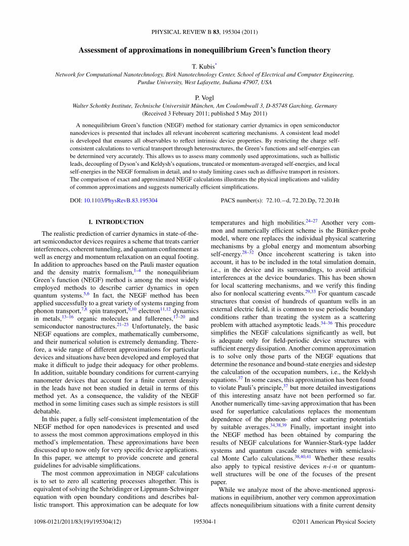
An obvious approximation in any NEGF calculation ofopen devices is to attach ballistic leads to the structure andinclude scattering only within the active device. This greatlysimplifies the calculations since the surface Green’s functionsof ballistic leads are analytically known.54–58 Figure 1 showsthe results of two different NEGF calculations of a piece ofhomogeneously n-doped GaAs of 50 nm length with attachedGaAs “leads” on both sides and in the absence of any appliedbias. Physically, this device simply represents homogeneousbulk GaAs in equilibrium that we have artificially dividedinto a “device” and two semi-infinite “leads.” The dopingconcentration is n = 1017 cm−3 and the lattice temperatureis set to 300 K. Correct calculations must obviously yield aconstant electron density throughout the device. Indeed, Fig. 1shows a constant electron density (solid line) but only in thecase in which scattering has been included within the leads
10 20 30 40 500.96
1.00
1.04
1.08
1.12
Position (nm)
Den
sity
(10
cm)
17-3
Scattering leads
Ballistic leads
FIG. 1. NEGF calculations of equilibrium electron density in ahomogeneously n-doped GaAs device with n = 1017 cm−3 at 300 K.The dashed line shows results for leads with ballistic electrons.They generate interference effects and nonhomogeneous densities. Aconsistent NEGF implementation (solid line) must include scatteringwithin the leads.
195304-4

ASSESSMENT OF APPROXIMATIONS IN . . . PHYSICAL REVIEW B 83, 195304 (2011)
self-consistently. By contrast, if we attach ballistic GaAs leadsto the piece of GaAs, the mismatch in the electronic density ofstates within the leads and within the device causes significantinterferences to occur near the device-lead interfaces, whichresults in an inhomogeneous electron density (dashed line).This result is a consequence of the density of states to becontrolled by the retarded Green’s function, which containsthe scattering self-energies. Therefore, a smooth, reflectionlessinterface requires matching the density of states between thedevice and the leads. This, in turn, requires a self-consistentcalculation of surface Green’s functions. Similar findings havebeen reported for slightly simplified NEGF calculations withscattering self-energies limited to local on-site scattering.29,33
B. Low-order self-energies
In the absence of vertex corrections to the self-energy thatwe have not included in the present implementation, we willfirst show that current conservation can only be guaranteedby implementing only self-energies that contain only fullyscattered Green’s functions. The most common scheme toachieve this self-consistency is the self-consistent Born ap-proximation. We will show this requirement by consideringthe following very simple momentum- and energy-conservingmodel self-energy:
� = αG, (16)
where α represents a scalar coupling constant that representssome type of perturbation and the index labels the three typesof Green’s functions and self-energies, ∈ {<,R,A}. Thematrix notation for G and � applies to the spatial coordinates(z,z′), whereas the momentum and energy coordinates �k‖,Eremain unchanged for this kind of coupling self-energy. Thespatial derivative of the current density is given by54
d
dzj (z)
∣∣∣∣z0
= − e
h(2π )2
∫dE
∫d2k‖I (z0,z0,k‖,E), (17)
where the integrand I reads in matrix form
I = �<GA − G<�A + �RG< − GR�<. (18)
When we truncate the perturbation series at the order n, theintegrand I reads
In = α[G<
n−1GAn − G<
n GAn−1 + GR
n−1G<n − GR
n G<n−1
]. (19)
The Green’s function of consecutive scattering orders onlyagrees in the limit n → ∞, i.e., in the self-consistent Bornapproximation
limn→∞ G
n = limn→∞ G
n−1. (20)
Only in this limit does the integrand in Eq. (19) vanish andthe current is exactly conserved. In any finite order n, on theother hand, the integrand is nonzero and can lead to substantialvariations of the current density along the device direction z.37
We note that additional approximations may be applied forthe Green’s functions in some situations that can restore thecurrent conservation in a truncated series expansion of theGreen’s functions.37,59 A violation of current conservation hasled some researchers to call the integral of Eq. (18) a scatteringcurrent jscatt and define a “total” current to be the sum of
−jscatt(z) and the correct current density j (z) of Eq. (4).60
While this quantity is spatially constant indeed, it bears norelation to the matrix element of the quantum-mechanicalvelocity operator and does not represent a converged resultfor the observable current density.61 We therefore believe thatthe NEGF formalism provides no simple way to avoid aninfinite summation over self-energies, i.e., the calculation offull Green’s functions, particularly in situations where thecurrent density is a crucial quantity.62 Finally, there is asubtlety to consider very close to the lead-device interface.While we have applied the self-consistent Born approximationin all calculations, the assumption of an analytic electrondistribution within the leads causes a violation of currentconservation very close to the lead-device interfaces sincethe self-energies are nonlocal. As a consequence, the currentdensity cannot be exactly conserved in the range of thisnonlocality around the device-lead interface. Fortunately, wefind this violation of the current conservation to be very smalland we typically achieve a relative current conservation ofbetter than 10−4.
C. Decoupled retarded and lesser Green’s functions
One of the cumbersome as well as numerically mostdemanding features of the NEGF formalism is the coupledsystem of Dyson and Keldysh equations. In particular, anyretarded self-energy �R associated with an inelastic-scatteringmechanism involves the lesser Green’s function G<. Thisraises the question of whether we can obtain a reasonableapproximation by leaving out all parts in �R that containG<. In this way, the system Eqs. (2) would get reduced to twoindependent sets of equations, which grossly reduces the effortof solving them. Such an approximation effectively impliesan independent determination of the resonant state energiesand their occupancies. If all state occupancies are small, suchan approximation appears to be reasonable, but Lake et al.have pointed out that this approximation may violate Pauliblocking.37 In this section, we will quantitatively analyze theeffect of this decoupling of the Dyson and Keldysh equationsin a concrete example.
We have performed an exact as well as a decoupled NEGFcalculation of the retarded and lesser functions in a laterallyhomogeneous, nanometer-sized heterostructure with attachedGaAs-type leads. The total length of the device is 50 nm,with a 16 nm intrinsic region embedded in between two17nm n-doped regions with n = 1018 cm−3 each. Within theintrinsic region, there is a 12 nm In0.14Ga0.86As quantum wellof 150 meV depth. To illustrate the occupation of bound states,we define a function f (z,k‖,E),
f (z,k‖,E) ≡ −iG<(z,z,k‖,E)/A(z,z,k‖,E), (21)
with the spectral function
A(z,z′,k‖,E) = i[GR(z,z′,k‖,E) − GR†(z,z′,k‖,E)]. (22)
In equilibrium, the function f (z,k‖,E) can be shown to beequal to the Fermi distribution f (E,μ).49 Note that thisfunction does not reflect the density of states but only theenergy- and position-dependent occupation function. It turnsout that the imaginary part of f (z,k‖,E) vanishes and its realpart is independent of k‖. Clearly, one expects the function
195304-5

T. KUBIS AND P. VOGL PHYSICAL REVIEW B 83, 195304 (2011)
Decoupled G ,G< R
-50 50 1000.0
0.5
1.0
1.5
2.0
Energy (meV)
Ele
ctro
n d
istr
ibu
tio
n f
(E
)
Fermi distribution
Full NEGF
10 20 30 40 50-80
-40
0
40 E2
µ
Position (nm)
Co
nd
uct
ion
ban
d (
meV
)
E1
0
FIG. 2. Equilibrium electron distribution within a 12-nm-wideGaAs/In0.14Ga0.86As quantum well embedded in n-doped GaAs at300 K calculated with fully self-consistent NEGF (solid line) andwith decoupled retarded and lesser Green’s functions (dashed),respectively. The zero in energy marks the chemical potential μ.The full NEGF result faithfully yields the Fermi distribution (graydots), in contrast to the decoupled model, which violates the Pauliprinciple. The inset shows the conduction-band edge along the devicewith a bound state E1 and a resonance state E2.
f (z,k‖,E) to be independent of position z. Indeed, this is thecase if the coupling between lesser and retarded functions isfully accounted for, but not so in the decoupled case.
Figure 2 shows the Fermi distribution (gray dots) and thereal part of the function f (z,k‖,E) in the exact (solid line) andthe approximated (dashed line) calculation in the middle ofthe In0.14Ga0.86As quantum well. The zero in energy marks thechemical potential of the device. If we include the full couplingof GR with G<, the calculation perfectly reproduces the Fermidistribution. By contrast, the decoupling of the Dyson andKeldysh equations yields a dramatic deviation from the Fermidistribution as soon as any occupancy exceeds a value of 0.3.The function f even exceeds its physical (Pauli blocking)limit of 1 for low-lying energies that are highly occupied.Since we assume a Fermi distribution in the leads, this triggersan artificial spatial inhomogeneity of f (z,k‖,E) when �R isapproximated to be independent of G<.
D. Effect of decoupling on Fermi’s Golden Rule
To further illustrate the physical implication of the de-coupling approximation of GR with G<, we will comparethe polar-optical-phonon scattering rate in bulk GaAs asobtained from a full and decoupled NEGF calculation withFermi’s Golden Rule. The polar optical phonon (LO-phonon)scattering self-energies are given in Eqs. (5) and (6). Weconsider homogeneously n-doped, unbiased GaAs with n =2 × 1018 cm−3 and set the zero in energy equal to the chemicalpotential. At zero and room temperature, this implies theband edge to lie at −86.42 and −79.06 meV, respectively.Even for this bulk system, we stick to the present coordinatesystem that is adapted to two-dimensional systems, but wehave checked that our calculations are able to reproduce the
known analytical formulas for the Green’s functions in bulksystems.63 In homogeneous devices, the Green’s functions andself-energies depend only on the difference of the propagationcoordinates (ζ = z − z′). This allows us to Fourier transformthe imaginary part of the retarded self-energy with respect toζ and obtain the scattering rate (see e.g., Ref. 64),
(k‖,kz,E) = −2
hIm
∫dζ exp(ikzζ )�R(ζ,k‖,E). (23)
In particular, we will analyze the on-shell scattering rate thatis obtained by evaluating at the vertical electron momentum,
kz =√
2m∗E/h2 − Ec − e� − k2‖ . (24)
This yields the on-shell scattering rate of electrons with kineticenergy h2(k2
‖ + k2z )/2m∗.
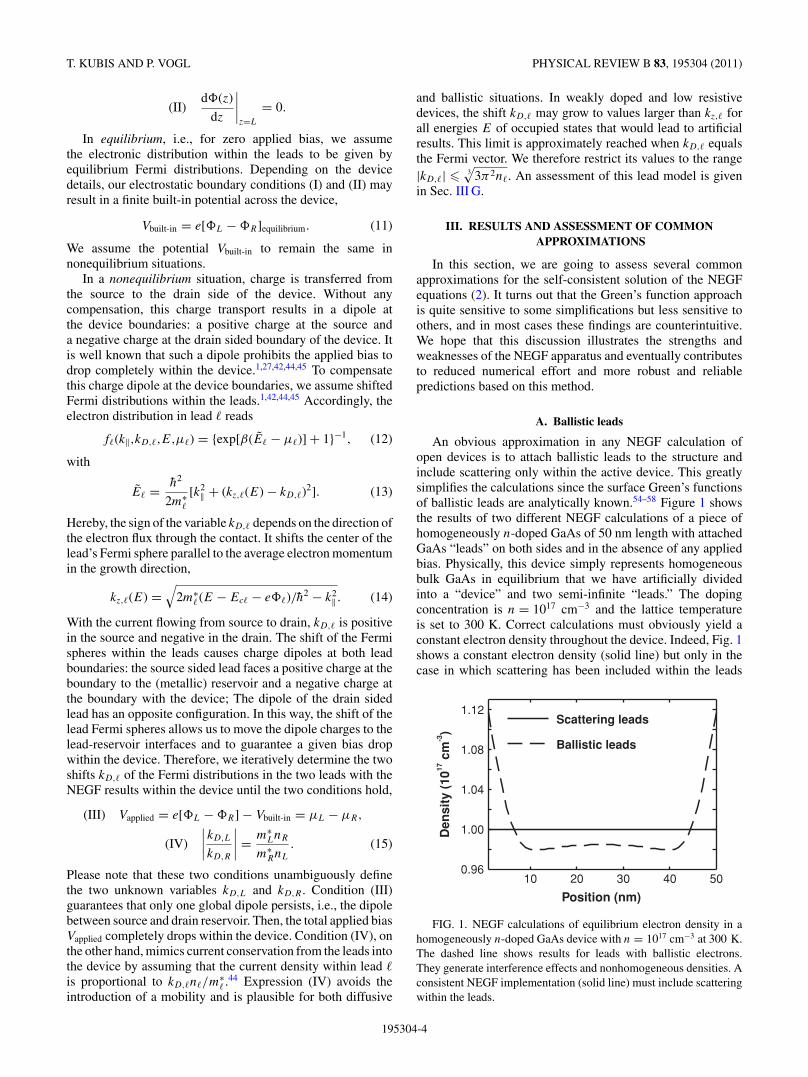
First, we consider temperature T = 0 so that only theemission of LO phonons is possible. Electrons at energieshigher than the LO-phonon energy E > hω0 as well as holeswithin the conduction band at energies lower than E < −hω0
are able to emit polar-optical phonons [see Fig. 3(a)]. Bycontrast, electrons and holes for intermediate energies −hω0 <
E < hω0 cannot emit phonons, because their respective finalstates are fully occupied.65 Consequently, scattering withLO phonons for electronic states in the interval [−hω0,hω0]is forbidden at T = 0. At room temperature, on the other
FIG. 3. (Color online) Calculated polar-optical-phonon scatteringin homogeneously n-doped GaAs with n = 2 × 1018 cm−3 at zerobias. The zero in energy marks the chemical potential. (a) Schematicpicture of allowed and forbidden scattering events at T = 0. Holes(open circles) and electrons (full circles) can only scatter within theindicated energy windows, set by the optical-phonon energy hω0.(b) Total on-shell optical-phonon scattering rate at 300 K. The exactNEGF calculation (solid line) agrees well with Fermi’s Golden Rule,i.e., first-order perturbation theory (large gray dots). The dashed lineresults from NEGF calculations with decoupled retarded and lesserGreen’s functions. The small black dots depict NEGF calculationswhere the nonlocality of the self-energy in real space with a spatialresolution of 1 nm has been neglected.
195304-6
ASSESSMENT OF APPROXIMATIONS IN . . . PHYSICAL REVIEW B 83, 195304 (2011)
hand, the electron distribution is significantly washed outand LO phonons can both be emitted and absorbed, sothat the suppression of scattering within the energy intervalof [−hω0,hω0] is less pronounced. The black solid line inFig. 3(b) shows the polar-optical-phonon scattering rate ofEqs. (23) and (6) that results from a fully self-consistent NEGFcalculation of this heavily n-doped GaAs. For comparison, thegray dots show the scattering rate that results from Fermi’sGolden Rule.51 For the latter, we have explicitly summedover the emission and absorption of LO phonons by electronsas well as the emission and absorption of LO phonons byholes within the conduction band. As one can deduce fromthis figure, Fermi’s Golden Rule closely follows the NEGFresult. This implies that higher-order scattering, which isincluded in the NEGF self-energy, plays only a minor rolein equilibrium and bulk GaAs due to the small polar-opticalcoupling constant. The situation is radically different for thedecoupled case. If all terms in the retarded self-energy Eq. (6)that contain G< are neglected, the scattering of holes in theconduction band as well as the suppression of scattering inthe energy interval [−hω0,hω0] are completely absent andthe scattering rate is grossly incorrect [see the dashed line inFig. 3(b)].
In conclusion, we find that the decoupling of inelasticretarded self-energies from G< is only applicable in situationsin which the occupation of all relevant electronic states issmaller than approximately 0.3. Otherwise, many particleeffects such as holelike scattering within the conduction bandand Pauli blocking become relevant. Even when the state oc-cupancy lies beneath this value, the retarded Green’s functionsand accordingly the retarded self-energies are influenced bythe lesser Green’s function via the Poisson potential. Thisdependence can safely be ignored only in very low-dopeddevices such as THz quantum cascade lasers.66
E. Local on-site self-energies
In the present real-space basis, all self-energies are nonlocalobjects that depend on the two spatial coordinates z and z′ inde-pendently (see Sec. II A).37,50,63 This increases the complexityof NEGF calculations significantly67 and hampers recursivealgorithms for the calculation of the Green’s functions.37,53 Wetherefore investigate here the consequences of limiting self-energies to on-site scattering.55,56,68 The black dotted line inFig. 3(b) shows results for the polar-optical-phonon scatteringrate of Eq. (23) where only on-site elements �(z,z,k‖,E),i.e., elements with ζ = 0, have been taken into account. Thecomparison with the exact NEGF result also shown in thisfigure shows that nonlocal scattering effects shift the totalscattering rate quantitatively, whereas the qualitative trendsremain intact, at least in this case. This result is consistentwith previous findings for resonant tunneling diodes.67
To quantify the nonlocal contributions, Fig. 4 illustratesthe imaginary part of the k‖-integrated lesser LO-phononself-energy �< in homogeneously n-doped bulk GaAs forvarious energies as a function of the distance ζ between the twopropagation coordinates z and z′ (cf. Fig. 3). This self-energy ismaximal close to the Fermi energy and decreases for energiesabove and below it. The dependence of �< on the energy E
is basically given by the energy-resolved density n(E) [see
0 1000
1
2
Energy (meV)
n(E) (arb. units)
-20 -10 0 10 20
0
4
8
12
Nonlocal range (nm)
E = 0E = -60 meV
E = 100 meV
Im<
2(k
,E)
dk
(arb
. un
its)
||||
FIG. 4. (Color online) Imaginary part of the lesser self-energy forelectronic scattering with polar-optical -phonons in homogeneouslyn-doped GaAs with n = 2 × 1018 cm−3 and at room temperature. Theself-energy is integrated over the in-plane momentum k‖ and shownfor various energies relative to the chemical potential as functionsof the difference of the two propagation coordinates ζ = z − z′. Thespatial resolution is 1 nm, but the lines are drawn continuously. Thedependence of �< as a function of energy E follows the energy-resolved density that is shown in the inset [see Eq. (3)].
Eq. (3)] shown in the inset of Fig. 4. Irrespective of theenergy, the nonlocal spread of the self-energy in the differencecoordinate ζ extends to approximately three times the devicescreening length (which amounts to 3 nm for the chosen dopingconcentration). We find very similar results for the retardedGreen’s function and for scattering by charged impurities.In devices where the carriers are confined by high barrierssuch as quantum cascade devices, on the other hand, thenonlocality is essentially limited to the width of the resonantstates, i.e., quantum-well widths. This is in agreement withprevious findings.69
F. Momentum-averaged self-energies
Since the integrals over the in-plane momentum l‖ inEqs. (5), (6), and (7) are numerically very demanding, it is anobvious and frequently implemented approximation to replacethe dependence of the coupling matrix elements Vimp(z,z′,k‖)and Vpop(z,z′,k‖) on the momentum transfer k‖ by an averagevalue �qtyp.34,38 To give an example, the retarded self-energyfor the interaction with charged impurities simplifies to
�Rimp(z,z′,k‖,E) = Vimp(z,z′,�qtyp)
∫dl‖l‖GR(z,z′,l‖,E).
(25)
While this approximation saves a lot of computer time, theenergy dependence of different scattering self-energies is nolonger specific to the physics of the scattering mechanism.37
In fact, the remaining energy dependence in the self-energiesresembles that for acoustic-phonon scattering and tends tounderestimate scattering of low-energy electrons and over-estimate it for electrons with high kinetic energies. Tofurther analyze this approximation, we consider the scatteringpotentials for the LO phonon Eq. (6) and charged impurityscattering Eq. (7) in homogeneous GaAs, respectively. Asshown in Fig. 5, the potentials vary significantly with k‖.
195304-7

T. KUBIS AND P. VOGL PHYSICAL REVIEW B 83, 195304 (2011)
0.0 0.2 0.4 0.6 0.8 1.00.0 0
1.0 40
2.0 80
3.0120
Transferred momentum k (nm )||-1
V(z
,z,k
) (a
rb. u
nit
s)p
op
||
V(z
,z,k
) (a
rb. u
nit
s)im
p||
q = 5 nmD-1
FIG. 5. Calculated scattering potentials for charged impurities(solid) and polar-optical phonons (dashed) at an in-plane momentuml‖ = 0.51 nm−1 as functions of the in-plane momentum k‖. Thescreening length q−1
D is set to 5 nm.
Obviously, the replacement by a constant �qtyp is not advisableand even a redetermination of this value for each voltage for agiven device is impractical.36
G. Lead electron distribution
We now discuss the impact of employing different leadmodels in NEGF calculations for open quantum systems. Inparticular, let us consider flat band boundary conditions forthe potential at the contacts and compare our present leadmodel that invokes a shifted Fermi distribution (model SF)with a model that employs an unshifted Fermi distribution(model UF).
Concretely, we study an 80-nm-wide laterally homoge-neous n++-i-n+ GaAs resistor at a temperature of 50 K. Fromleft to right, we take a 32-nm-wide n-doped region with n =2 × 1018 cm−3, followed by a 10.7 nm intrinsic GaAs layerand, finally, a 37.3-nm-wide n-doped region with n = 1 ×1018 cm−3 [see Fig. 6(a)]. The asymmetry of this structureyields a build-in potential of Vbuilt-in = −34.2 meV. By apply-ing a bias voltage of +34.2 mV, both lead conduction-bandedges should be exactly equal if the applied voltage dropsentirely within the device. For each of the two models,Figs. 6(a) and 6(b) depict the self-consistently calculatedelectron densities and conduction-band profiles, respectively.
The results for model UF are shown by dotted lines.Figure 6(b) reveals that the difference of the source and drainconduction-band edges in this model is far from zero and doesnot correctly reflect the applied bias. Indeed, it is known thatthe assumption of equilibrium electron distributions within theleads causes a charge dipole at the device boundaries and anincomplete bias drop across the device.42,45
In contrast, the black solid lines depict results for caseSF, which is the presently employed lead model, describedin Sec. II B. In this case, the potential drop within the devicematches exactly the applied bias voltage. Another importantconsequence of choosing a shifted Fermi distribution withinthe leads is shown in Fig. 7. This figure shows the calculatedcurrent density for the two lead models UF (dotted line) andSF (solid line), respectively. Since the shifted lead Fermidistributions increase the average electron velocity of the
doping density
= 0, k = 0D
= 0, k = 0.022 nmD,L-1
(b)
(a)0.5
1.0
1.5
2.0
Den
sity
(10
cm)
18-3
2.5
20 40 60 80-20
-10
0
10
20
30
40
50
Position (nm)
Co
nd
uct
ion
ban
d (
meV
)
V = -34.2 meVbuilt-in
(Model SF)(Model UF)
FIG. 6. (Color online) NEGF results for (a) the electron densityand (b) the self-consistently determined conduction-band profile fortwo different lead models. The doping has been chosen so thatthe built-in potential exactly compensates the applied bias. Theconduction-band edges in (b) should therefore lie at zero energy at thedevice boundaries. The dotted lines correspond to a lead model withequilibrium lead electron distributions and vanishing electric fields atthe boundaries (model UF), as described in the main text. The blacksolid lines show results of the presently proposed lead model SF thatincludes shifted lead electron distributions.
0 40 80 120 160 2000
1
2
3
4
5
6
Applied bias voltage (mV)
Cu
rren
t d
ensi
ty (
MA
/cm
)2 , k > 0 (Model SF)D= 0
, k = 0 (Model UF)D= 0
V(z)
zr||
n++n+
i
FIG. 7. Current density as a function of applied bias voltage forthe same n++-i-n+ resistor as in Fig. 6. NEGF calculations with leadmodel UF corresponding to equilibrium leads (dotted line) predictsignificantly smaller current densities than those with the presentlyproposed lead model SF that is based on self-consistently shifted leadFermi distributions (solid line).
195304-8

ASSESSMENT OF APPROXIMATIONS IN . . . PHYSICAL REVIEW B 83, 195304 (2011)
00.0
0.02
0.04
0.06
1 2 3 4 5 6
Current density (MA/cm )2
k(n
m)
D,L
-1
V(z)
zr||
n++n+
i
FIG. 8. Self-consistently determined shift of the Fermi distribu-tion in the left contact of the n++-i-n+ resistor of Fig. 6 as a functionof current density.
carriers in the device, the current density is larger than inthe case of unshifted Fermi distributions.In fact, the low-fieldmobility μ is almost twice as large in the currently employedlead model (SF) (μ ∼ 2286 cm2 V−1 s−1) as in model UFwith unshifted Fermi distributions (μ ∼ 1330 cm2 V−1 s−1).Part of the reason for this finding lies in the incompletepotential drop within the device.27,43 In addition, the vanishingaverage momentum of lead electrons in case UF representsan additional serial resistance that also reduces the currentdensity.
Interestingly, we find the self-consistently determinedmomentum shifts kD,� of the Fermi distribution in the leadsto be almost linearly related to the current density. Figure 8shows kD,L of the present n++-i-n+ structure as a functionof the current density. The almost linear relation betweenthe momentum kD,L and current density is consistent withprevious lead models and may simplify the determination of asuitable shift of the Fermi distribution.44
Finally, we show results that one obtains by not enforcingflat band boundary conditions for the potentials at the contactsand invoking unshifted contact Fermi distributions. For thedevice we are considering in this section, charge neutralityonly dictates the electric field to be the same at bothcontacts,
d�(z)
dz
∣∣∣∣z=R
= d�(z)
dz
∣∣∣∣z=L
.
We may determine the magnitude of this electric field byrequiring the applied potential to drop entirely within thedevice, i.e., by condition III in Eq. (15). The resulting chargedensity and conduction-band energy as a function of positionwithin the device is depicted in Fig. 9. This figure revealsan artificial pinch-off near the left device boundary and acharge accumulation near the right boundary, which are clearlyartifacts of the chosen lead model. This result is a consequenceof the lower average velocity of the carriers within the contactsas compared to the situation within the device, where they getaccelerated by the electric field. This clearly demonstrates theimportance of a consistent global treatment of the electrondistribution both inside the contacts and within the activedevice region.
doping density
= 49.3 kV/cm, k = 0D
(b)
(a)0.5
1.0
1.5
2.0
Den
sity
(10
cm)
18-3
2.5
20 40 60 80-20
-10
0
10
20
30
40
50
Position (nm)
Co
nd
uct
ion
ban
d (
meV
)
FIG. 9. NEGF results for (a) the electron density and (b) theself-consistently determined conduction-band profile for a lead modelwith unshifted equilibrium electrons within the contacts but withnonvanishing electric fields at the boundaries. This model leads tounphysical charge depletions and accumulations, as discussed in themain text.
H. Semiclassical limit
The stationary current characteristics of our simplen++-i-n+ resistor are well described by semiclassical trans-port, particularly since it is larger than 10 nm in size anddoes not contain any bound states.27,31,32 Consequently, aself-consistent NEGF calculation should yield results in closeagreement with the solution of the Boltzmann equation,provided we employ the same type of scattering mechanismsand matrix elements. Given the fact that a NEGF calculationis far from being physically transparent, such a comparisonis of utmost relevance for judging and understanding therobustness and reliability of the NEGF method. Figure 10shows the electron density of the present n++-i-n+ resistorthat results from the NEGF method (circles) and from thesolution of the semiclassical Boltzmann equation (solid line),respectively. The excellent agreement of both results confirmsthat the NEGF method correctly yields the limiting case ofquasiclassical systems. Previous work on stationary electrontransport in superlattices and quantum cascade lasers hasshown that semiclassical transport models may even agreewith NEGF calculations in systems with confined states, whenthe transport is dominated by incoherent scattering.38,40,41
In passing, we would like to point out that all results inthis paper have been obtained within the NEGF approach.A semiclassical calculation has only been performed for thecomparison in Fig. 10.
195304-9

T. KUBIS AND P. VOGL PHYSICAL REVIEW B 83, 195304 (2011)
20 40 60 800.4
0.8
1.2
1.6
2.0
Position (nm)
Den
sity
(10
cm)
18-3
NEGF
Boltzmann equation
FIG. 10. Equilibrium electron density of the n++-i-n+ GaAsresistor of Fig. 6 for zero bias. The result of the NEGF calculation isdepicted by open circles and agrees excellently with the solution ofthe semiclassical Boltzmann equation (solid line).
IV. CONCLUSION
In this work, we have implemented and assessed theNEGF method for stationary electron transport in opensemiconductor nanodevices by including incoherent scatteringon LO and acoustic phonons and charged impurities. AllGreen’s functions are dressed by incorporating scattering toinfinite order, and their nonlocal nature as well as their fullenergy and momentum dependence are taken into account. Ithas been demonstrated that the electron distribution within theleads must be self-consistently adjusted to the current densityin the device in order to obtain physically meaningful results.Our calculations indicate that the density of states within theleads must be matched to that in the device to obtain resultsthat reflect the intrinsic physics of the device. This typicallyrequires the numerical solution of the lead’s surface Green’sfunctions. Many frequently implemented approximations havebeen assessed in some detail. The present study suggests thatthe coupling between the retarded and lesser Green’s functionmay be neglected when Pauli blocking plays no role, i.e.,the state occupancy is less than 30% for all device states. Inaddition, we have found that the nonlocality of the self-energiesin a position basis can be limited to approximately threetimes the screening length or to the typical extension ofconfined states in devices with high barriers. Unfortunately,the calculations also showed that the energy and momentumdependence of scattering self-energies is difficult to neglector approximate. In summary, the present work sheds newlight on the strengths and weaknesses of the nonequilib-rium Green’s functions method that may help in its futureapplications.
ACKNOWLEDGMENTS
This work has been supported by the Austrian Scien-tific Fund FWF (SFB-IRON), the Deutsche Forschungs-gemeinschaft (SFB 631 and SPP 1285), the ExcellenceCluster Nanosystems Initiative Munich, and the NationalScience Foundation (Grants No. OCI-0749140, No. EEC-0228390, and No. ECCS-0701612). Computational resourcesof nanoHUB.org are gratefully acknowledged.
APPENDIX: GENERALIZED LEAD MODEL
In the following, we generalize the lead model presented inSec. II B to general device dimensions and an arbitrary numberof leads. We separate our system into a device of volume � andits surroundings. We denote the device boundary by δ� andits surface normal with �η. Charge carriers can enter or leavethe device through N reservoirs that are coupled to the devicevia N leads. We use the term contact δ�c,� for the intersectionof lead � ∈ {1, . . . ,N} and the device and define
δ�c =N⋃
�=1
δ�c,�. (A1)
The remaining device surface, i.e.,
δ�c = δ� \ δ�c, (A2)
acts as a barrier of infinite height. We solve the Poissonequation in the device under the condition of vanishing electricfields perpendicular to the device surface,
(I) [ �∇�(�x)] · �η(�x)|δ� = 0. (A3)
This condition automatically implies global charge neutralityof the device, ∫
δ�
ε(�x)[ �∇�(�x)] · �η(�x)d�x = 0. (A4)
To guarantee charge neutral leads, the doping density close toδ� is assumed to be sufficiently high so that all electric fields ofthe device interior that are parallel to �η(�x) are screened withinthe device. Please note that the electrostatic fields parallelto the device surface may still be finite. In equilibrium, weassume the electrons in each lead to be distributed accordingto a single Fermi function. Still, we allow the self-consistentsolution of the electron density and the Poisson equation toresult in a finite built-in potential Vbuilt-in(�x) at �x ∈ δ�. Innonequilibrium, we assign individual chemical potentials μ�
to each lead,
μ�(�x)|δ�c,�= μ�, (A5)
and use the following shifted distribution of electrons in lead� (analogous to Sec. II B):
f�(�k,E) ={
exp
[β
(h2
2m∗�(E)
|�k − �kD,�|2 − μ�
)]+ 1
}−1
.
(A6)
Hereby, we assume a homogeneous energy-dependent effec-tive mass m∗
�(E) in the lead �. The vector �kD,� lies perpendi-cular to the contact,
�kD,� = kD,��η�. (A7)
The shifts of the lead distributions are determined implicitlyfrom the condition that the bias drops completely within thedevice,
(II) e
∫δ�c,�
[�(�x) + Vbuilt-in(�x)]d�x − μ�
= κ,(� = 1,2, . . . ,N ). (A8)
195304-10

ASSESSMENT OF APPROXIMATIONS IN . . . PHYSICAL REVIEW B 83, 195304 (2011)
To determine the variable κ , we assume the current densityin the lead � to be proportional to a product of the shift kD,�,the inverse energy averaged effective mass 〈m∗
�〉−1, and theelectron density n(�x) integrated along the contact area δ�c,�.Since the total amount of current density that flows into thedevice has to flow out of it again, the variable κ has to be
determined such that the global current is conserved. Thisleads to the condition
(III)N∑
�=1
kD,�〈m∗�〉−1
∫δ�c,�
n(�x)d�x = 0. (A9)
*[email protected]. V. Fischetti, J. Appl. Phys. 83, 270 (1998).2C. Weber, A. Wacker, and A. Knorr, Phys. Rev. B 79, 165322(2009).
3H. Willenberg, G. H. Dohler, and J. Faist, Phys. Rev. B 67, 085315(2003).
4R. C. Iotti and F. Rossi, Phys. Status Solidi B 238, 462 (2003).5L. P. Kadanoff and G. Baym, Quantum Statistical Mechanics(Benjamin, Menlo Park, CA, 1962).
6L. V. Keldysh, Sov. Phys. JETP 20, 1018 (1965).7Y. Xu, J.-S. Wang, W. Duan, B.-L. Gu, and B. Li, Phys. Rev. B 78,224303 (2008).
8N. Mingo, Phys. Rev. B 74, 125402 (2006).9M. Yamamoto, T. Ohtsuki, and B. Kramer, Phys. Rev. B 72, 115321(2005).
10N. Sergueev, Q.-F. Sun, H. Guo, B. G. Wang, and J. Wang, Phys.Rev. B 65, 165303 (2002).
11M. Luisier, A. Schenk, and W. Fichtner, J. Appl. Phys. 100, 043713(2006).
12V. N. Do, P. Dollfus, and V. L. Nguyen, J. Appl. Phys. 100, 093705(2006).
13Z. Chen, J. Wang, B. Wang, and D. Y. Xing, Phys. Lett. A 334, 436(2005).
14Y. Ke, K. Xia, and H. Guo, Phys. Rev. Lett. 100, 166805(2008).
15W. Belzig, F. K. Wilhelm, C. Bruder, G. Schon, and A. D. Zaikin,Superlatt. Microstruct. 25, 1251 (1999).
16T. Frederiksen, M. Paulsson, M. Brandbyge, and A.-P. Jauho, Phys.Rev. B 75, 205413 (2007).
17T. Sato, K. Shizu, T. Kuga, K. Tanaka, and H. Kaji, Chem. Phys.Lett. 458, 152 (2008).
18P. Damle, A. W. Gosh, and S. Datta, Chem. Phys. 281, 171 (2002).19H. Li and X. Q. Zhang, Phys. Lett. A 372, 4294 (2008).20G. Schull, T. Frederiksen, M. Brandbyge, and R. Berndt, Phys. Rev.
Lett. 103, 206803 (2009).21X. Zheng, W. Chen, M. Stroscio, and L. F. Register, Phys. Rev. B
73, 245304 (2006).22P. Havu, M. J. Puska, R. M. Nieminen, and V. Havu, Phys. Rev. B
70, 233308 (2004).23M. Lazzeri, S. Piscanec, F. Mauri, A. C. Ferrari, and J. Robertson,
Phys. Rev. Lett. 95, 236802 (2005).24D. Mamaluy, D. Vasileska, M. Sabathil, T. Zibold, and P. Vogl,
Phys. Rev. B 71, 245321 (2005).25T. Zibold, P. Vogl, and A. Bertoni, Phys. Rev. B 76, 195301
(2007).26B. K. Nikolic, S. Souma, L. P. Zarbo, and J. Sinova, Phys. Rev. Lett.
95, 046601 (2005).27Z. Ren, R. Venugopal, S. Datta, M. Lundstrom, D. Jovanovic, and
J. Fossum, IEDM Tech. Digest (2000), pp. 715–718.28M. Buttiker, Phys. Rev. B 33, 3020 (1986).29S. Sato and N. Sano, J. Comput. Electron. 7, 301 (2008).
30S. Wang and N. Mingo, Phys. Rev. B 79, 115316 (2009).31M. Lundstrom and Z. Ren, IEEE Trans. Electron Dev. 49, 133
(2002).32Z. Ren, R. Venugopal, S. Goasguen, S. Datta, and M. Lundstrom,
IEEE Trans. Electron Dev. 50, 1914 (2003).33M. Frey, A. Esposito, and A. Schenk, in Proceedings of the 13th
International Workshop on Computational Electronics (IWCE-13),(IEEE, Beijing, 2009), pp. 17–20.
34S.-C. Lee and A. Wacker, Phys. Rev. B 66, 245314 (2002).35N. Vukmirovic, Z. Ikonic, D. Indjin, and P. Harrison, Phys. Rev. B
76, 245313 (2007).36T. Schmielau and M. F. Pereira, Phys. Status Solidi B 246, 329
(2009).37R. Lake, G. Klimeck, R. C. Bowen, and D. Jovanovic, J. Appl. Phys.
81, 7845 (1997).38A. Wacker, A.-P. Jauho, S. Rott, A. Markus, P. Binder, and G. H.
Dohler, Phys. Rev. Lett. 83, 836 (1999).39A. Wacker, Phys. Status Solidi C 5, 215 (2008).40A. Wacker and A.-P. Jauho, Phys. Rev. Lett. 80, 369 (1998).41A. Matyas, T. Kubis, P. Lugli, and C. Jirauschek, Physica E 42,
2628 (2010).42W. Potz, J. Appl. Phys. 66, 2458 (1989).43S. Datta, Superlatt. Microstruct. 28, 253 (2000).44S. E. Laux, A. Kumar, and M. V. Fischetti, J. Appl. Phys. 95, 5545
(2004).45W. R. Frensley, Rev. Mod. Phys. 62, 745 (1990).46W. Potz, J. Appl. Phys. 71, 2297 (1992).47M. V. Fischetti, Phys. Rev. B 59, 4901 (1999).48G. Klimeck, J. Comput. Electron. 2, 177 (2003).49H. Haug and A.-P. Jauho, Quantum Kinetics in Transport and Optics
of Semiconductors (Springer, Berlin, 1996).50T. Kubis, C. Yeh, P. Vogl, A. Benz, G. Fasching, and C. Deutsch,
Phys. Rev. B 79, 195323 (2009).51B. K. Ridley, Quantum Processes in Semiconductors (Oxford
Science Publications, Oxford, 1982).52This implies that we approximate the lesser surface Green’s
function in each lead by (−1)f (GRS − G
R†S ), where f is the lead
electron distribution and GRS is the retarded surface Green’s
function.53A. Svizhenko, M. P. Anantram, T. R. Govindan, B. Biegel, and
R. Venugopal, J. Appl. Phys. 91, 2343 (2002).54S. Datta, Electronic Transport in Mesoscopic Systems (Cambridge
University Press, Cambridge, 1995).55R. Venugopal, M. Paulsson, S. Goasguen, S. Datta, and M. Lund-
strom, J. Appl. Phys. 93, 5613 (2003).56A. A. Yanik, G. Klimeck, and S. Datta, Phys. Rev. B 76, 045213
(2007).57R. Golizadeh-Mojarad and S. Datta, Phys. Rev. B 75, 081301(R)
(2007).58Y.-S. Liu, H. Chen, X.-H. Fan, and X.-F. Yang, Phys. Rev. B 73,
115310 (2006).
195304-11
T. KUBIS AND P. VOGL PHYSICAL REVIEW B 83, 195304 (2011)
59M. Paulsson, T. Frederiksen, and M. Brandbyge, J. Phys. Conf. Ser.35, 247 (2006).
60T. Schmielau and M. F. Pereira, Appl. Phys. Lett. 95, 231111(2009).
61S.-C. Lee, F. Banit, M. Woerner, and A. Wacker, Phys. Rev. B 73,245320 (2006).
62K. S. Thygesen and A. Rubio, Phys. Rev. B 77, 115333 (2008).63T. Kubis, Quantum Transport in Semiconductor Nanostructures,
edited by G. Abstreiter, M. C. Amann, M. Stutzmann, andP. Vogl (Verein zur Forderung des Walter Schottky Institutsder Technischen Universitat Munchen e.V., Garching, 2009);[http://nanohub.org/resources/8612].
64A. Wacker, Phys. Rep. 357, 1 (2002).
65G. D. Mahan, Many-Particle Physics (Plenum, New York, 1990).66A. M. Andrews, A. Benz, C. Deutsch, G. Fasching, K. Unterrainer,
P. Klang, W. Schrenk, and G. Strasser, Mater. Sci. Eng. B 147, 152(2008).
67G. Klimeck, R. Lake, C. L. Fernando, R. C. Bowen, D. Blanks,M. Leng, T. Moise, Y. C. Kao, and W. R. Frensley, in Proceedingsof the International Conference on Quantum Devices and Circuits:Alexandria, Egypt, 1996, edited by K. Ismail, S. Bandyopadhyay,and J. P. Leburton (World Scientific, London, 1997).
68S. Jin, Y. J. Park, and H. S. Min, J. Appl. Phys. 99, 123719(2006).
69S.-C. Lee, F. Banit, M. Woerner, and A. Wacker, Phys. Rev. B 73,245320 (2006).
195304-12