dye sensitised anocrystalline solar ... - uni …€¦ · 117 dye-sensitised nanocrystalline solar...
TRANSCRIPT
117
DYE-SENSITISED NANOCRYSTALLINE SOLAR CELLS
Augustin J. McEvoy and Michael GrätzelLaboratory for Photonics and Interfaces,
Department of Chemistry,Ecole Polytechnique Fédérale de Lausanne
The dominant photovoltaic device at the present time is the solid state junction, in which thematerials and concepts of semiconductor technology are applied to the challenge of cost-ef-fective solar energy conversion into electricity. An alternative approach is electrochemical,with semiconductor contacts to electrolytes sensitised to visible light by charge transfer dyes.The principle of operation of the sensitised photoelectrochemical device has close affinity tophotography, and depends for its future development on materials science on the nanometricscale, and on molecular engineering to provide dyes with the energetics, chemical kineticsand absorption match to the solar spectrum, if it is to successfully enter the market in compe-tition with the established products.
1. Sunshine, Photovoltaics and Photosynthesis
Any discussion of photovoltaic technology and its future utility as part of the overall energymarket must begin with an objective assessment of the solar energy conversion problem andthe adequacy of the solution proposed. Solar irradiation provides an annual energy input toour planet of 1.56 x 10¹⁸ kWh, in comparison with which our annual primary energy con-sumption is smaller by a factor of 104. However, this energy is distributed, non-uniformly,over the total surface of the earth, so obviously in practice it is not constantly available on agiven area, and has a maximum power, at midday under a clear tropical sky, of only 1kW/m2.A commercial photovoltaic system has a typical conversion efficiency of the order of 10 -15%, so a panel giving 1 kW output under peak insolation (1 kWp) has an area of at least7m2. Taking account of higher latitude, seasonal and weather considerations at a centralEuropean site, the typical annual electrical output of a photovoltaic system is about 800kWhper installed kWp of PV modules. There remains also the problem of load matching, giventhat power supplied by a PV system under our conditions is not coincident with maximumdemand, and therefore conventional systems must remain available to maintain supply conti-nuity, since an adequate technology for large-scale storage of electrical energy is not yetavailable. It follows that if PV is in the future to become a significant component of a Euro-pean energy system, the solar energy panels must have a very large area, associated with lowcost and extremely high reliability, as the economics of competition with other technologiesdemands a mimimum lifetime of several decades under outdoor conditions - extremes of tem-perature, wind, snow and hailstorms, as well as corrosion and even vandalism!
118
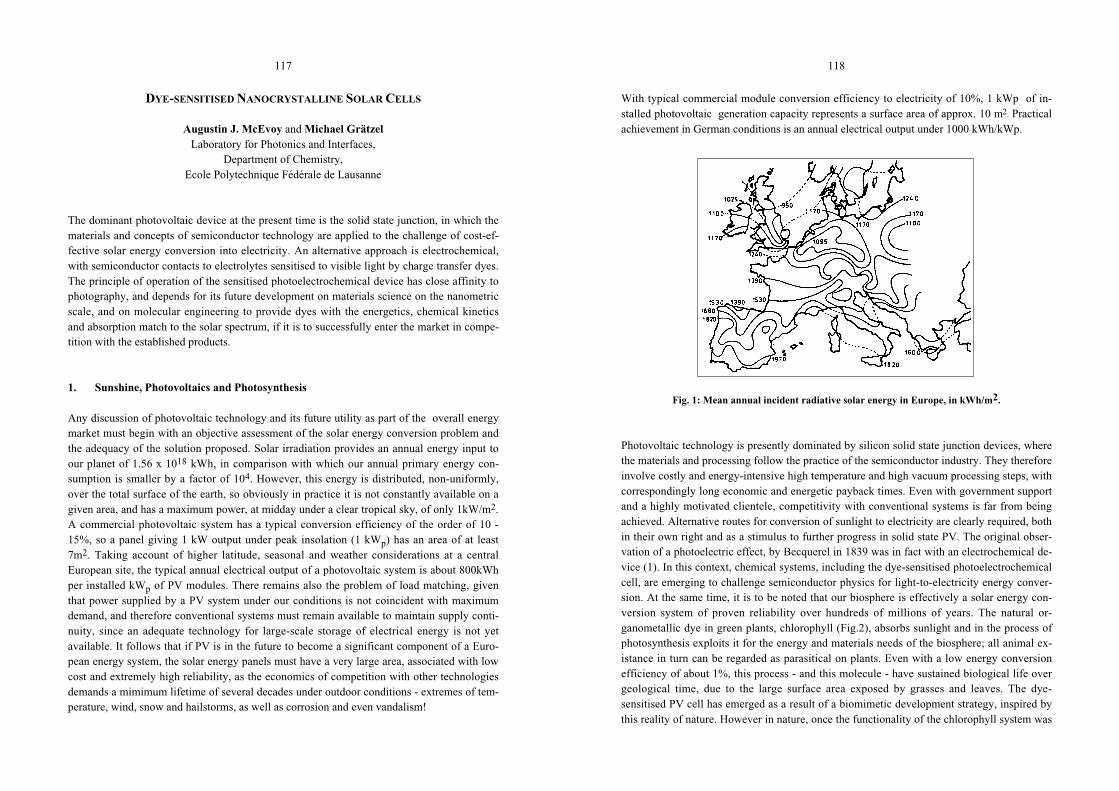
With typical commercial module conversion efficiency to electricity of 10%, 1 kWp of in-stalled photovoltaic generation capacity represents a surface area of approx. 10 m2. Practicalachievement in German conditions is an annual electrical output under 1000 kWh/kWp.
Fig. 1: Mean annual incident radiative solar energy in Europe, in kWh/m2.
Photovoltaic technology is presently dominated by silicon solid state junction devices, wherethe materials and processing follow the practice of the semiconductor industry. They thereforeinvolve costly and energy-intensive high temperature and high vacuum processing steps, withcorrespondingly long economic and energetic payback times. Even with government supportand a highly motivated clientele, competitivity with conventional systems is far from beingachieved. Alternative routes for conversion of sunlight to electricity are clearly required, bothin their own right and as a stimulus to further progress in solid state PV. The original obser-vation of a photoelectric effect, by Becquerel in 1839 was in fact with an electrochemical de-vice (1). In this context, chemical systems, including the dye-sensitised photoelectrochemicalcell, are emerging to challenge semiconductor physics for light-to-electricity energy conver-sion. At the same time, it is to be noted that our biosphere is effectively a solar energy con-version system of proven reliability over hundreds of millions of years. The natural or-ganometallic dye in green plants, chlorophyll (Fig.2), absorbs sunlight and in the process ofphotosynthesis exploits it for the energy and materials needs of the biosphere; all animal ex-istance in turn can be regarded as parasitical on plants. Even with a low energy conversionefficiency of about 1%, this process - and this molecule - have sustained biological life overgeological time, due to the large surface area exposed by grasses and leaves. The dye-sensitised PV cell has emerged as a result of a biomimetic development strategy, inspired bythis reality of nature. However in nature, once the functionality of the chlorophyll system was

119
established as adequate to provide the energy to maintain a self-replicating organism, thatmolecule was retained despite the ongoing variation in plant structure, environment andgenetics. There is a similar history over geological time for the haemoglobin molecule inanimals, also a nitrogen-cage structure or porphyrin surrounding a metal, in this case iron. Toemulate photosynthesis on the other hand there is no restriction of the metal or thesurrounding organic complex, giving endless possibilities for molecular engineering of dyes.
Fig. 2: Molecular structure of chlorophyll, the key to natural photosynthesis.
2. Sensitisation of Semiconductors
It could be asked why the use of a dye is necessary in chemical or electrochemical photocon-version devices. In the solid state cell, the semiconductor is at the same time the optical ab-sorber of photons whose energy exceeds the band gap, and the site of charge separation toprovide a photovoltage across a junction, p-n within the material or Schottky at a metal-semi-conductor interface. On energy considerations, a semiconductor-electrolyte contact in a pho-tochemical system is identical to the Schottky case, the redox potential of the electrolyte be-ing the equivalent of the metal Fermi level. However, semiconductors with band gaps appro-priate for the absorption and conversion of sunlight are liable to photocorrosion in contactwith electrolytes; since positively charged holes arrive at the interface the species with whichthey are most likely to react oxidatively may be the semiconductor itself, unless the kineticsof the redox reaction are sufficiently fast to provide some degree of protection. Semiconduc-tors with wide band gaps, and therefore stable under illumination in contact with electrolytes,are poorly matched to the solar spectrum; titanium dioxide, one of the better candidates, has aband gap of 3.1 eV., and therefore an optical absorption edge already in the ultraviolet. Asso-ciation of the semiconductor with a separate optical absorber such as a suitable dye could thenprovide a photoeffect with visible light.
120
This particular problem was already well known in the physics of photography, contemporaryin its origins, in the work of Daguerre (1837) and Fox-Talbot (1831) with the photoelectricobservations of Becquerel. Silver halides were established as the standard photosensitive ma-terials, but the formulation of photographic emulsions remained an art rather than a sciencefor a further century, until the theory of the process was presented by Gurney and Mott in1938 (2). However the limitations of early emulsions were gradually overcome, notable theinability to present realistically on a grey scale scenes observed in colour, given their insensi-tivity to mid-spectral and red light. It is now known that this is due to the wide bandgaps ofthe silver halide semiconductor grains, over 2.7 eV. Extension of the spectral response pro-ceeded empirically, with the observation that the origin of the gelatin in the emulsion had adistinct effect. Only in this century was it recognised that organosulfur compounds in calf-skin gelatin were responsible, by producing a sulfide layer of wider sensitivity on each halidegrain (3). A more systematic approach was followed by Vogel, as professor of photochemis-try, spectroscopy and photography at the Königliche Technische Hochschule in Berlin to-wards the end of the 19th. Century. From 1873 onwards he researched the association of dyeswith the silver halide grains, finding a photoresponse controllably extended into the red andeven the infrared, making possible the panchromatic black-and- white (or more accurately,grey-scale) film and ultimately, with spectrally selective dyes, the modern colour film (4).
Fig. 3: The first report in the scientific literature of the optical sensitisation of a semiconductor,silver chloride, the obvious choice because of its use in photography (Moser, Vienna, 1887).

121
Possibly influenced by these developments, and using the same silver halide semiconductors,the first sensitisation of a photoelectric effect was also reported over a century ago, in the textreproduced above (5). For the physics community it is instructive to note that Moser, writing20 years before the Einstein theory of the photoelectric effect, correctly referred tosensitisation of the electrical current, which we now know to be proportional to the radiativeintensity or flux of photons, but he reported his result in volts, although the photopotential isprimarily a function of the semiconductor band-gap and is linked only indirectly with theintensity through carrier loss processes.
Fig. 5: Schematic of operation of the dye-sensitised electrochemical photovoltaic cell. Thenanoporous sensitised semiconductor photoanode receives electrons from the photoexcited dye
which is thereby oxidised. The charge-neutral state is restored by reaction with the redoxelectrolytewhich in turn is regenerated by reduction at the metallic cathode by the electrons
circulated through the external circuit.
This historic parallel maintained between sensitisation in photography and in photoelectro-chemistry still seems to come as a surprise (6). That the same dyes were particularly effectivefor both processes was recognised amongst others by Namba and Hishiki (7) at the 1964 In-ternational Conference on Photosensitisation in Solids in Chicago, which was a seminal eventin the history of dyes in photochemistry It was also important for the presentation of a theo-retical understanding of sensitisation, since it was still disputed whether the mechanism wasan electron transfer or an energy-coupling process. The presently accepted model was deter-mined shortly after in the work of Gerischer and Tributsch (8,9) on ZnO, which left little fur-ther doubt about the mechanism, and the significance for photoelectrochemistry of the dye-sensitisation phenomenon. It is now evident that the process involved the excitation of the dyefrom its charge-neutral ground state to an excited state by the absorption of the energy of aphoton. One of the permitted relaxation processes is the injection of an electron into the va-lence band of the semiconductor, leaving the dye molecule positively charged. In the photo-graphic process the injected electron reduces a silver ion, and thereby established the latent
-0.5
1.0
0
0.5
E / V vs NHE
S°/S+
S*
hν
maximumvoltage
mediator
TiO2 electrolyte cathode
interception
dye
injection
red ox
diffusion
conductingglass
P. Bonhôte / EPFL-LPI
122
image. In a photoelectrochemical cell, the injected electrons form a current in an external cir-cuit, reaching a cathode in contact with the redox electrolyte. The uncharged ground state ofthe dye is in turn restored by electron transfer from the redox system, completing the circuitand providing a regenerative cycle functionally comparable with other photovoltaic devices,as presented in fig. 5.
The dye has clearly a charge transfer function, but it is not itself an electrical conductor.Therefore only molecules in intimate contact with the substrate can engage in the electron in-jection process. However, a monomolecular layer is not sufficient effectively to absorb theincident light for photovoltaic conversion of energy. This requirement of sufficient opticaldensity of the absorbing structure leads to the use of nanocrystalline materials for the titaniumdioxide semiconductor; by provision of an extended surface area, sufficient dye, chemisorbedas a monomolecular layer, can be retained on a given area of electrode to provide absorptionto opacity of the incident light. The semiconductor structure, typically 10__ thick and with aporosity of 50%, therefore has a surface available for dye chemisorption enhanced by a factorof several hundred in comparison with the projected electrode surface area, due to that nano-scale crystallinity. From the micrograph, fig. 6, the grain size in a photoelectrode is under 10nanometers; smaller grain size is evidently associated with enhanced surface area.
Fig. 6: SEM image of the surface of a mesoporous film preparedfrom a hydrothermally processed TiO2 colloid.
It followed then to recognise that the major loss mechanism associated with polycrystalline orrough semiconductors in photovoltaics, the recombination of the photoexcited electrons withthe mobile positive holes in the crystalline lattice or at surface or grain boundaries, is not ap-plicable to the dye-sensitised electrochemical device (10). In amorphous silicon solar cells thesuppression of recombination is carried out by reacting unsaturated bonds with hydrogen orfluorine. In the dye-sensitisation case, in contrast, no specific action is necessary, as the elec-tron injected from the photoexcited dye finds itself in the semiconductor lattice, separated
100 nm

123
spatially and by a potential barrier from the oxidised dye species (Fig. 5) within picosecondsof the optical excitation event. The carrier loss mechanisms are comparatively slow (11), andalthough conventionally referred to as recombination, by analogy with the solid-state process,the loss of a photoexcited electron from the semiconductor should be regarded as a recaptureby an oxidised dye species, or a redox capture when the electron reacts directly with an ion inthe electrolyte. Either occurs on a millisecond timescale. This extreme ratio of the kinetics ofthe photovoltaic process to those of loss mechanisms is essential if the required cell lifetime isto be maintained. In the case of the photovoltaic device, at least 108 cycles through the rege-nerative process of photoexcitation of the sensitising dye, electron injection and neutralisationof the charged state by the redox electrolyte are required in a typical 20 years of outdoor ope-ration, in contrast with the single cycle of the photographic process. This vividly illustratesthe constraints for development of practical photovoltaic dyes.
3. Semiconductor Film Processing
As already mentioned, titanium dioxide is one of the better candidates for use as a sensitisablesemiconductor. Work in Lausanne began with an investigation of TiO2 as substrate for achemisorbed sensitizing dye, first on particles (12) in the 1980's, then on photoelectrodes(13). The material has many advantages for sensitized photochemistry and photoelectro-chemistry: it is a low cost, widely available, non-toxic material, and as such is even used inhealth care products. The original semiconductor film used for our early photosensitizationexperiments (14), a fractal derived by hydrolysis of an organo-titanium compound, has sincebeen replaced with a nanostructure deposited from colloidal suspension. This evidently pro-vides a much more reproducible and controlled porous high surface area nanotexture. Further,since it is compatible with screen printing technology for deposition on a conducting trans-parent substrate, it anticipates future production requirements. Hydrothermal techniques areemployed for the synthesis of the nanoparticulate anatase TiO2 powder used in colloidal fromas the screen printing ink for dye solar cell fabrication, a technology which is continuouslyevolving to yield film microstructures which increase the photovoltaic performance of suchdevices through better optical management. Other oxide semiconductors which have beenstudied in the context of dye sensitized photovoltaics include ZnO, SnO2, Nb2O5, and SrTiO3
(15-19).
The microstructure of the semiconductor is of course a compromise, to achieve an optimaloptical absorption and photovoltaic performance. Nanosize grains give the greatest surfacearea, but pores must be sufficiently large that the mobility of the charge carriers in the elec-trolyte, the redox ions, is not unduly inhibited. Also some degree of optical scattering bylarger particles in the semiconducture film is also desirable, particularly for devices whichfunction under indirect illumination such as vertical building facades. Processing parameters
124
Table 1: Flow diagram for the preparation of TiO2 colloids and mesoporous films.
such as precursor chemistry, hydrothermal growth temperature for the titania powder, andsintering conditions are varied in the optimisation precedure. A flowsheet for hydrothermalprocessing is presented in Table 1 as an example of the required development work, and infig.7 the control of grain size which results from it, as determined by a nitrogen adsorptionmethod.
Fig. 7: Influence of hydrothermal growth temperature of TiO2 colloids on the pore sizedistribution. Curves obtained from N2 desorption data using the BJH model.
3-roll mill, 15 minutes
Modify Ti-isopropoxide with acetic acid
Rapidly add precursor to water
Acidify with HNO3, reflux
Autoclave: 12 hours at 230°C
Rotovap: 45°C, 30mbar
Anneal: 450°C, 20 minutes
Flocculation, centrifuging
Hydrothermal Growth
Solvent Exchange,Ethyl Cellulose Addition
Dry and Anneal Films
Peptization
Hydrolysis
Precursor Preparation
Homogenize Paste
Concentrate Colloid
Screen Print Films
0
1 0 0 0
2 0 0 0
3 0 0 0
4 0 0 0
5 0 0 0
6 0 0 0
7 0 0 0
8 0 0 0
9 0 0 0
0 1 0 2 0 3 0 4 0 5 0 6 0 7 0 8 0
190°C2 1 02 3 02 5 02 7 0
Diff
eren
tial
Volu
me
((cm
3 /g)/
nm)
[10-5
]
Pore Diameter (nm)

125
Fig.8: Structure of dye-sensitised photoelectrochemical cell on different scales. (Top): acomplete cell (centimetric scale). (Centre):electrodes and electrolyte, micron scale.
(Bottom): nanocrystalline semiconductor interconnected porous layer,with adsorbed monolayer of dye and entrained electrolyte (nano scale).
For the photoanode, the screen printed pattern using the hydrothermally grown powder in anink is sintered to the conducting glass substrate, and the dye monomolecular layer applied.The cathode or counter-electrode is usually a similar glass, treated to electrocatalyse the redoxreaction, for example with highly dispersed platinum. The cell is completed with an edge seal
126
to contain the electrolyte, usually a liquid although gel or solid variants are also possible. Cellstructure on successively smaller scales is shown in fig. 8, ultimately reaching the moleculardimensions of the dye itself.
4. Dye Development
The constraints determining the dye selection have already been indicated, and the productionof a suitable formulation is a demanding exercise in synthetic chemistry. Firstly and evidentlythere is the matter of an optical absorption spectrum closely matched to the application of thephotovoltaic device, whether it be to the solar spectrum for energy conversion or to artificiallight sources for indoor use. With a high optical absorption coefficient across the visiblespectrum, the excitation process should be rapid but subsequent relaxation slow, as alreadyexplained. For attachment to the semiconductor surface the molecule should adsorb strongly,by preference through a specific chemical bond, to the substrate, but avoid aggregation so thata monolayer coverage forms spontaneously on contact between the semiconductor and thedye in solution. To facilitate this chemisorption, carboyxlate or phosphonate groups, whichbind strongly to titanium sites in the oxide, are integrated into the dye molecule. The dyestructures selected for intensive development arose originally from biomimetic considera-tions, given the role of photosynthesis in the natural world. However, whereas plant photo-synthetic processes rely on chlorophyll, a magnesium organometallic molecule, the syntheticchemist can select from the whole range of complex-forming metals to design an appropriatemetal-ligand charge transfer structure. When develoment of the photovoltaic device started,ruthenium pyridyl complexes were already attracting considerable interest as photochemicalreagents (20), so they have since been the principal focus of dye sensitiser development.
Fig.9: The photocurrent action spectrum of a cell containing various sensitizers, where theincident photon to current conversion efficiency is plotted as a function of wavelength.
127
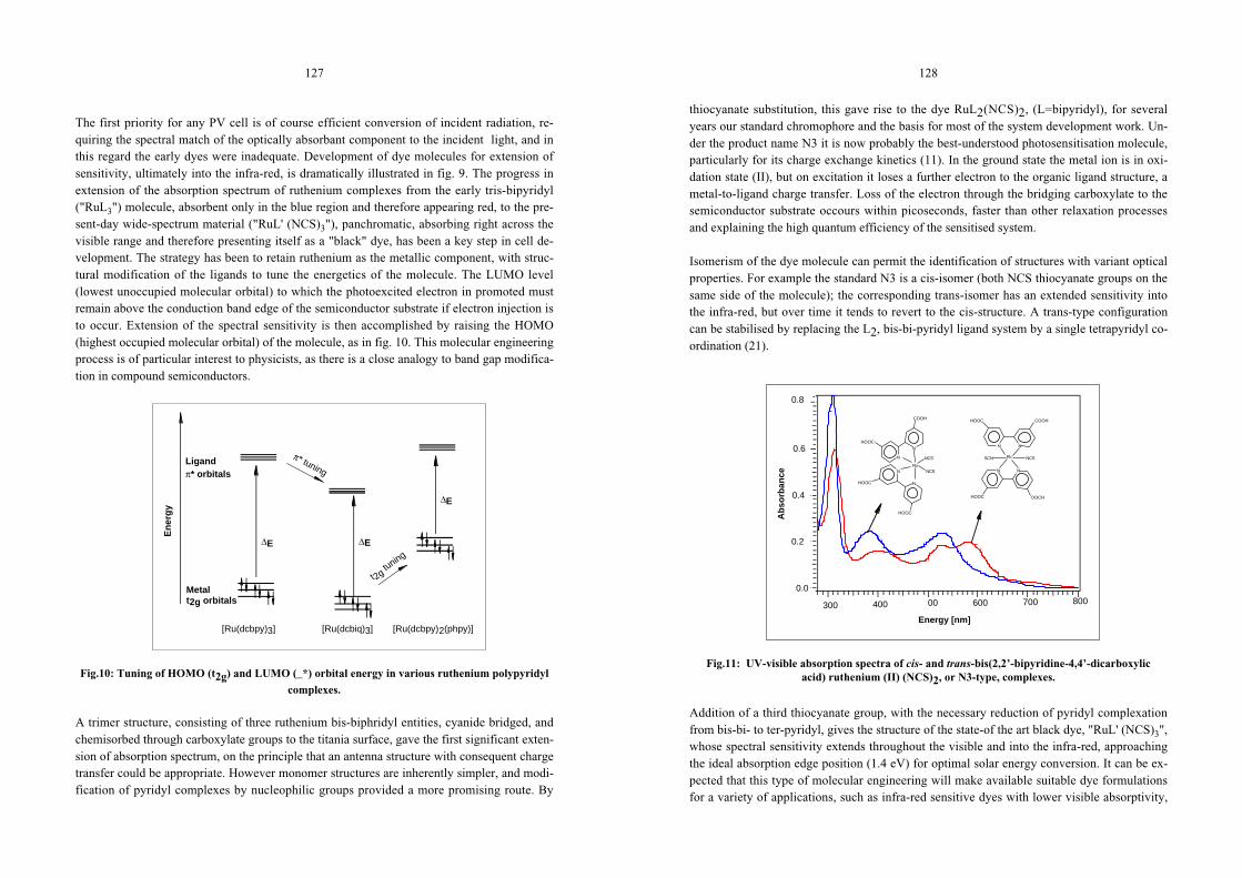
The first priority for any PV cell is of course efficient conversion of incident radiation, re-quiring the spectral match of the optically absorbant component to the incident light, and inthis regard the early dyes were inadequate. Development of dye molecules for extension ofsensitivity, ultimately into the infra-red, is dramatically illustrated in fig. 9. The progress inextension of the absorption spectrum of ruthenium complexes from the early tris-bipyridyl("RuL3") molecule, absorbent only in the blue region and therefore appearing red, to the pre-sent-day wide-spectrum material ("RuL' (NCS)3"), panchromatic, absorbing right across thevisible range and therefore presenting itself as a "black" dye, has been a key step in cell de-velopment. The strategy has been to retain ruthenium as the metallic component, with struc-tural modification of the ligands to tune the energetics of the molecule. The LUMO level(lowest unoccupied molecular orbital) to which the photoexcited electron in promoted mustremain above the conduction band edge of the semiconductor substrate if electron injection isto occur. Extension of the spectral sensitivity is then accomplished by raising the HOMO(highest occupied molecular orbital) of the molecule, as in fig. 10. This molecular engineeringprocess is of particular interest to physicists, as there is a close analogy to band gap modifica-tion in compound semiconductors.
Fig.10: Tuning of HOMO (t2g) and LUMO (_*) orbital energy in various ruthenium polypyridyl
complexes.
A trimer structure, consisting of three ruthenium bis-biphridyl entities, cyanide bridged, andchemisorbed through carboxylate groups to the titania surface, gave the first significant exten-sion of absorption spectrum, on the principle that an antenna structure with consequent chargetransfer could be appropriate. However monomer structures are inherently simpler, and modi-fication of pyridyl complexes by nucleophilic groups provided a more promising route. By
Metal t2g orbitals
En
erg
y
∆E
Ligand π* orbitals
∆E
π* tuning
∆E
t 2g tuning
[Ru(dcbpy)3] [Ru(dcbiq)3] [Ru(dcbpy)2(phpy)]
128
thiocyanate substitution, this gave rise to the dye RuL2(NCS)2, (L=bipyridyl), for severalyears our standard chromophore and the basis for most of the system development work. Un-der the product name N3 it is now probably the best-understood photosensitisation molecule,particularly for its charge exchange kinetics (11). In the ground state the metal ion is in oxi-dation state (II), but on excitation it loses a further electron to the organic ligand structure, ametal-to-ligand charge transfer. Loss of the electron through the bridging carboxylate to thesemiconductor substrate occours within picoseconds, faster than other relaxation processesand explaining the high quantum efficiency of the sensitised system.
Isomerism of the dye molecule can permit the identification of structures with variant opticalproperties. For example the standard N3 is a cis-isomer (both NCS thiocyanate groups on thesame side of the molecule); the corresponding trans-isomer has an extended sensitivity intothe infra-red, but over time it tends to revert to the cis-structure. A trans-type configurationcan be stabilised by replacing the L2, bis-bi-pyridyl ligand system by a single tetrapyridyl co-ordination (21).
Fig.11: UV-visible absorption spectra of cis- and trans-bis(2,2’-bipyridine-4,4’-dicarboxylicacid) ruthenium (II) (NCS)2, or N3-type, complexes.
Addition of a third thiocyanate group, with the necessary reduction of pyridyl complexationfrom bis-bi- to ter-pyridyl, gives the structure of the state-of the art black dye, "RuL' (NCS)3",whose spectral sensitivity extends throughout the visible and into the infra-red, approachingthe ideal absorption edge position (1.4 eV) for optimal solar energy conversion. It can be ex-pected that this type of molecular engineering will make available suitable dye formulationsfor a variety of applications, such as infra-red sensitive dyes with lower visible absorptivity,
0.8
0.6
0.4
0.2
0.0
Ab
sorb
ance
80070060000400300
Energy [nm]
N
N
HOOC
COOH
N
N
HOOC
HOOC
RuNCS
NCS
N N
COOH
Ru
HOOC
NN
OOCHHOOC
NCSSCN

129
useful for "transparent" cells, or dyes with selective absorption, the resulting color presenta-tion being determined for example by architectural preference for building-integrated PV.
Fig. 12: Certified performance characteristics of a "black dye" [RuL'(NCS) 3] cell.
The interaction between the dye molecule and the adsorbant surface also influences the ener-getics of the dye and the kinetics of its chemical reactions. For example it is known that onadsorption of a carboxylated dye, a titania surface becomes positively charged, due to the de-protonation of the acid dye. The consequent interface potential gradient obviously enhanceselectron injection efficiency, leading to a higher photocurrent. However efficiency does notproportionately rise, since the positive shift of band edge is associated with a lower open-cir-cuit voltage. Optimisation of the cell efficiency also requires a control of protonation of the
PFL (Switzerland) nano-crystal dye sensitized cell
Sample: PL0710/2 Temperature = 25.0oCOct 30, 1998 10:41 AM Area = 0.1863 cm2
ASTM E 892-87 Global Irradiance: 1000.0 Wm-2
Voc = 0.7210 V Imax = 3.552 mA
Jsc = 20.53 mAcm-2 Fill Factor = 70.41%
Vmax = 0.5465 VIsc = 3.824 mA Pmax = 1.941 mWEfficiency = 10.4 %
tape aperture, “black” dye
130
dye. With this in mind several salts of N3 with organic cations such as tetrabutylammoniumand imidazolium have been investigated (21). These salts are also more soluble, facilitatingpurification by recrystalisation and thereafter adsorption to the semiconductor from the moreconcentrated solution. The thermal dehydration behaviour shows the association of only 1.5molecules of water per Ru ion, for the optimum di-tetrabutylammonium salt, with a thermalstability thereafter to 190˚C; at that point the organic cation tends to dissociate. When ad-sorbed on the semiconductor the dye stability is further enhanced, decarboxylation requiringover 300˚C. This remarkable rise is attributed to the strength of the Ti ion to carboxylate bondbetween the semiconductor surface and the chemisorber molecule. This confirmation of thethermal stability of the surface-bonded dye therefore opens the prospect of a very wide tem-perature window for processing the sensitised semiconductor during any manufacturing rou-tine, simplifying bonding and sealing processes by permitting thermal treatment and curing ofsealants even after the dye has been admitted to the cell.
Modification of the surface of the semiconductor to optimise adsorption and charge transferbehaviour is a further option. Several years ago, deposition of an outer intrinsic titania (22) ora solid solution layer (23) on the semiconductor was investigated in order to control the inter-face properties after dye adsorption. Evidently a nanostructure emulating the oxide or insula-tor layer in MOS or MIS solid state Schottky devices has a similar effect in defining thebandedge characteristics in the photoelectrochemical case.
5. Solid State Heterojunctions
Given that a dye at the interface in a photoelectrochemical cell can sensitise the system tophotons of lower energy that would not otherwise be absorbed by the semiconductor, the pos-sibility presents itself that the same effect could be verifiable at a semiconductor interface to adifferent conducting phase. Here we are not considering the special cases of gel or polymerelectrolytes (24), because in these charge transport is by the same mechanism as in a conven-tional liquid electrolyte. The sensitised solid state cell, while functionally similar, requires acontact between the n-type titania semiconductor substrate and a metal or p-type semicon-ductor. Since the sensitising dye provides charge separation but not charge transport, and isdistributed at an interface in the form of an immobilised molecular species, it is evident thatfor charge transfer each molecule must be in intimate contact with both conducting phases.This applies in the first instance to the wide bandgap porous semiconductor substrate intowhich the photoexcited chemisorbed molecules inject electrons. It is also evident that in thephotoelectrochemical format of the sensitised cell the liquid electrolyte penetrates into the po-rosity, thereby permitting the required intimate contact with the charged dye molecule neces-sary for charge neutralisation after the electron loss by exchange with the redox system insolution. It is not immediately evident that an interpenetrating network of two conductingsolids can be established so easily that an immobilised molecule at their interface can ex-change charge carriers with both. This is a

131
Fig. 13: structure of spirobifluorene hole-conducting p-type organic semiconductor. Theflourene structures are perpendicular, conjoined through a carbon site common to both.
particular obstacle to the realisation of a sensitised nanostructured Schottky junction. How-ever use of transparent organic semiconductors is a possibility, and initial results in our labo-ratory (25) and elsewhere (26) are promising. In both cases the hole conducting p-type mate-rials are deposited by spin coating from the liquid phase in order to achieve the necessary in-timate contact. In the latter case a mixture of polymers was used, which phase-separate spon-taneously on removal of a solvent, whereas the Lausanne laboratory introduces a solution ofthe conducting compound into a previously-sensitised nanostructure. The charge transfer ma-terial currently used is a spirobifluorene, proprietary to Hoechst (27) as shown in Fig. 13. As amatter of technical precision, if this materials functions in the cell as a hole conductor, the de-vice constitutes a sensitised nanostructured heterojunction.
6. Applications for Sensitised Photovoltaic Devices
Commercial success is not an immediate and necessary consequence of the development of atechnically elegant system. Therefore the efficiency and stability of the dye solar cell must beassociated with practical and economic advantages. On the technical side, the efficiency ofconventional solid state junction cells falls off rapidly with increasing temperature and de-creasing light intensity, whereas the sensitised system remains more constant under both op-erating parameter variables. The cell fabrication processes are intrinsically less demanding -no high vacuum or high temperature treatment steps, with therefore a low "grey" energy de-mand, whereas silicon devices require up to 5 gigaJoules per square meter of cell surface. Theenergy recovery time for the sensitised system should therefore be distinctly shorter. For ar-chitectural applications the possibility to select for cell color, even transparency, and texturegives additional freedom of action in building design, and with the incorporation of a light
N
N
NN
OCH3
OCH3
OCH3
OCH3
OCH3
OCH3
OCH3
OCH3
132
diffusive function, by admixture of large grains in the semiconductor layer for example, theeffect of variation of light incidence angle can be less marked. The cells may be bifaciallysensitive, thereby capable of increased output when mounted over high albedo surfaces. Fi-nally even on the parameter of energy conversion efficiency amorphous silicon is alreadysuccessfully challenged, even though crystalline silicon cells may still retain a margin of ad-vantage. To illustrate this competitivity, in fig. 14 the incident photon conversion efficiencyspectrum of a state of the art dye photoelectrochemical cell is compared with those of newand of aged a-Si solid state devices under daylight conditions.
Fig. 14: Spectral response, given as incident photon conversion efficiency against wavelength, of
a dye-sensitised cell () in comparison with a new (-------) or used (……, 800 W/m2)amorphous silicon cell.
A second area of competitivity is for indoor devices, under artificial light. In the dye-sensi-tised cell one of the parameters most difficult to optimise is the fill factor, related as it is toion diffusivity in the electrolyte and therefore to its viscosity. The lower intensity under artifi-cial light indoors is advantageous for the sensitised device, as its conversion efficiency ismaintained or even raised, whereas that of conventional junctions falls aff as the open-circuitvoltage decreased in those circumstances. Behavior under indoor conditions, including undera variety of artificial light sources, is compared with that of a-Si cells in fig.15.

133
7. Conclusion
Whereas the total solar energy input to earth is extremely high, at a given site the energy den-sity is low and intermittent, a fact which constrains its integration into the energy economy,particularly in the absence of a high-volume energy storage technology. To compensate forthese difficulties and to compete technically and economically with more conventional pro-cesses, solar photovoltaic systems must be of large area, low cost, and very high long-termreliability. It is not therefore a simple technology to implement. Stimulation of imaginativeenergy conversion procedures for electricity production from sunlight is therefore highly de-sirable, and the emergence of the dye-sensitised photoelectrochemical solar cell is thereforenot only of interest in its own right, but is also just that type of stimulus required, both to mo-tivate advances in solid state devices, and also as a verification that alternative procedures arepossible.
Fig. 15: Comparison of power outputs of a dye-sensitised nanocrystalline photoelectrochemicalcell and of a-Si devices, new and aged, under typical indoor illumination from natural or
artificial sources.
134
The use of dye-sensitised semiconductors has a long development history, in parallel for im-age and information storage through photography and now as an energy conversion techno-logy through applied photochemistry to rival the established solid state devices. The photo-electrochemical system, and the related dye-sensitised heterojunction. In some aspects thevarious solar energy conversion devices may be regarded as having complementary advan-tages, so that market possibilities specific to the sensitised systems can be expected toemerge. After a decade of gestation, therefore, the sensitised cell is now approaching techni-cal maturity, so commitment to production is now more a question of commercial judgement,not technical limitation.
8. Acknowledgements
It is evident that the development of a new technical concept is a team effort, here involvingspecialisations from ceramic thin film processing to organometallic synthesis. Many of thecollaborators in this effort are cited in the references below. Their efforts are appreciated. Re-search and development are impossible without resources and institutional support.The SwissFederal Office of Energy funded the initial work on this concept; thereafter several industrieshave shown their confidence in its potential by licensing the relevant patents. Internationalinterest is reflected by the engagement of the European Office of Aerospace Research andDevelopment, Air Force Office of Scientific Research, and Materials and Manufacturing Di-rectorate, United States Air Force Research Laboratory, and of the European Union withinFramework Programme 5 in association with other research institutes and industry.

135
REFERENCES
1. E.Becquerel, C.R.Acad.Sci. Paris 9 (1839) 561.
2. R.W.Gurney and N.E.Mott, Proc.Roy.Soc., A164 (11938) 151.
3. T.H.James, Theory of the Photographic Process,4th. Ed., MacMillan, New York, 1977.
4. W.West, Proc. Vogel Cent. Symp., Photog. Sci. Eng., 18 (1974) 35.
5. J.Moser, Monatsh. Chem., 8 (1887) 373.
6. M.T.Spitler, J.Chem.Ed., 60 (1983) 330.
7. S. Namba and Y. Hishiki, J.Phys.Chem., 69 (1965) 774.
8. H. Tributsch, Ph.D. thesis, Techn.Hochschule München (1968).
9. H. Gerischer and H. Tributsch, Ber. Bunsenges, Phys.Chem., 72 (1968) 437.
10. A.J. McEvoy, in “Advances in Solar Energy”, W.H. Bloss and F. Pfisterer (Eds); Proc.Intern. Solar Energy Soc., Hamburg (1987), Pergamon, Oxford (1988), p. 2921.
11. S.A.Haque, Y.Tachibana, R.L.Willis, J.E.Moser, M.Grätzel, D.R.Klug and J.A.Durrant,J.Phys.Chem.B, 104 (2000) 538.
12. D. Duonghong, N. Serpone and M. Grätzel, Helv.Chim.Acta, 67 1012 (1984).
13. H. DeSilvestro, M. Grätzel, L. Kavan, J. Moser and J. Augustynski, J.Am.Chem.Soc.,107 (1985) 2988.
14. N. Vlachopoulos, P. Liska, A.J. McEvoy and M. Grätzel, Surface Sci, 189/90 (1987)823-831.
15. I. Bedja, S. Hotchandani, P.V. Kamat, J. Phys. Chem., 98 (1994).4133.
16. K. Sayama, H. Sugihara and H. Arakawa, Chem. Mater. 10 (1998) 3825.
17. B. O’Regan and D. T. Schwartz, J. Appl. Phys., 80 (1996) 4749.
18. H. Rensmo, K. Keis, H. Lindstrom, S. Sodergren, A. Solbrand, A. Hagfeldt, S.-E.Lindquist, L.N. Wang and M. Muhammed J. Phys. Chem.B , 101 (1997) 2598.
19. R.Dabestani, A.J.Bard, A.Campion, M.A.Fox, T.E.Mallouk, S.E.Webber andJ.M.White, J. Phys. Chem., 92 (1998) 1872.
20. M. P. Dare-Edwards, J.B.Goodenough, A.Hamnett, K.R.Seddon and R.D.Wright,Faraday Disc. Chem. Soc., 70 (1980) 285.
21. M.K.Nazeeruddin, S.M.Zakeeruddin, R.Humphrey-Baker, M.Jirouzek, P.Liska, N.Vlachopoulos, V.Shklover, C.-H.Fischer and M. Grätzel, Inorg. Chem., 38 (1999) 6298.
136
22. US patent 5525440 (1996).
23. US patent 5350644 (1994).
24. S.Mikoshiba, H.Sumino, M.Yonetsu and S.Hayase, Proc.16th. Europ. PV Solar EnergyConf., Glasgow, Scotland, May 2000, page. 47.
25. U.Bach, D.Lupo, P.Comte, J.E.Moser, F.Weissörtel, J.Salbeck, H.Spreitzert andM.Grätzel, Nature 395 (1998) 544.
26. J.J.M.Halls, C.A.Walsh, N.C.Greenham, E.A.Marseglia, R.H.Friend, S.C.Moratti andA.B.Holmes, Nature 376 (1995) 498.
27. European patent PCT/ EP96/03944