dual/quad input network clock …...dual/quad input network clock generator/synchronizer data sheet...
TRANSCRIPT

Dual/Quad Input Network Clock Generator/Synchronizer
Data Sheet AD9547
FEATURES Supports Stratum 2 stability in holdover mode Supports reference switchover with phase build-out Supports hitless reference switchover Automatic/manual holdover and reference switchover 2 pairs of reference input pins, with each pair configurable
as a single differential input or as 2 independent single-ended inputs
Input reference frequencies from 1 kHz to 750 MHz Reference validation and frequency monitoring (1 ppm) Programmable input reference switchover priority 30-bit programmable input reference divider 2 pairs of clock output pins, with each pair configurable as
a single differential LVDS/LVPECL output or as 2 single-ended CMOS outputs
Output frequencies up to 450 MHz 20-bit integer and 10-bit fractional programmable feedback
divider Programmable digital loop filter covering loop bandwidths
from 0.001 Hz to 100 kHz Optional low noise LC-VCO system clock multiplier Optional crystal resonator for system clock input On-chip EEPROM to store multiple power-up profiles Software controlled power-down 64-lead LFCSP package
APPLICATIONS Network synchronization Cleanup of reference clock jitter SONET/SDH clocks up to OC-192, including FEC Stratum 2 holdover, jitter cleanup, and phase transient
control Stratum 3E and Stratum 3 reference clocks Wireless base stations, controllers Cable infrastructure Data communications
GENERAL DESCRIPTION The AD9547 provides synchronization for many systems, including synchronous optical networks (SONET/SDH). The AD9547 generates an output clock that is synchronized to one of two differential or four single-ended external input references. The digital PLL allows for reduction of input time jitter or phase noise associated with the external references. The AD9547 continuously generates a clean (low jitter), valid output clock, even when all references fail, by means of digitally controlled loop and holdover circuitry.
The AD9547 operates over an industrial temperature range of −40°C to +85°C.
FUNCTIONAL BLOCK DIAGRAM
REFERENCE INPUTSAND
MONITOR MUX
STATUS ANDCONTROL PINS
SERIAL CONTROL INTERFACE(SPI or I2C) EEPROM
DIGITALPLL
CLOCK DISTRIBUTION
SYNC
DAC
CLOCKMULTIPLIER
STABLESOURCE
ANALOGFILTER
AD9547
CHANNEL 0DIVIDER
CHANNEL 1DIVIDER
0830
0-00
1
Figure 1.
Rev. G Document Feedback Information furnished by Analog Devices is believed to be accurate and reliable. However, no responsibility is assumed by Analog Devices for its use, nor for any infringements of patents or other rights of third parties that may result from its use. Specifications subject to change without notice. No license is granted by implication or otherwise under any patent or patent rights of Analog Devices. Trademarks and registered trademarks are the property of their respective owners.
One Technology Way, P.O. Box 9106, Norwood, MA 02062-9106, U.S.A. Tel: 781.329.4700 ©2009–2014 Analog Devices, Inc. All rights reserved. Technical Support www.analog.com
AD9547 Data Sheet
Rev. G | Page 2 of 106
TABLE OF CONTENTS Features .............................................................................................. 1
Applications ....................................................................................... 1
General Description ......................................................................... 1
Functional Block Diagram .............................................................. 1
Revision History ............................................................................... 3
Specifications ..................................................................................... 4
Supply Voltage ............................................................................... 4
Supply Current .............................................................................. 4
Power Dissipation ......................................................................... 4
Logic Inputs (M0 to M7, RESET) ............................................... 5
Logic Outputs (M0 to M7, IRQ) ................................................ 5
System Clock Inputs (SYSCLKP, SYSCLKN)............................ 5
Distribution Clock Inputs (CLKINP, CLKINN) ...................... 6
Reference Inputs (REFA/REFAA, REFB/REFBB) .................... 7
Reference Monitors ...................................................................... 7
Reference Switchover Specifications .......................................... 8
Distribution Clock Outputs (OUT0, OUT1) ........................... 8
DAC Output Characteristics (DACOUTP, DACOUTN) ....... 9
Time Duration of Digital Functions ........................................ 10
Digital PLL .................................................................................. 10
Digital PLL Lock Detection ...................................................... 10
Holdover Specifications ............................................................. 10
Serial Port Specifications—SPI Mode ...................................... 11
Serial Port Specifications—I2C Mode ...................................... 12
Jitter Generation ......................................................................... 13
Absolute Maximum Ratings .......................................................... 14
ESD Caution ................................................................................ 14
Pin Configuration and Function Descriptions ........................... 15
Typical Performance Characteristics ........................................... 18
Input/Output Termination Recommendations .......................... 23
Getting Started ................................................................................ 24
Power-On Reset .......................................................................... 24
Initial M0 to M7 Pin Programming ......................................... 24
Device Register Programming .................................................. 24
Theory of Operation ...................................................................... 26
Overview ...................................................................................... 26
Reference Clock Inputs .............................................................. 27
Reference Monitors .................................................................... 27
Reference Profiles ....................................................................... 28
Reference Switchover ................................................................. 30
Digital Phase-Locked Loop (DPLL) Core ............................... 32
Direct Digital Synthesizer (DDS) ............................................. 34
Tuning Word Processing ........................................................... 35
Loop Control State Machine ..................................................... 36
System Clock Inputs ................................................................... 37
SYSCLK PLL Multiplier ............................................................. 38
Clock Distribution ..................................................................... 39
Status and Control .......................................................................... 44
Multifunction Pins (M0 to M7) ............................................... 44
IRQ Pin ........................................................................................ 45
Watchdog Timer ......................................................................... 45
EEPROM ..................................................................................... 46
Serial Control Port ......................................................................... 51
SPI/I2C Port Selection ................................................................ 51
SPI Serial Port Operation .......................................................... 51
I2C Serial Port Operation .......................................................... 56
I/O Programming Registers .......................................................... 59
Buffered/Active Registers .......................................................... 59
Autoclearing Registers ............................................................... 59
Register Access Restrictions ...................................................... 59
Register Map ................................................................................... 60
Register Bit Descriptions ............................................................... 70
Serial Port Configuration and Part Identification (Register 0x0000 to Register 0x0005) ...................................... 70
System Clock (SYSCLK) (Register 0x0100 to Register 0x0108).......................................................................... 71
General Configuration (Register 0x0200 to Register 0x0214).......................................................................... 72
DPLL Configuration (Register 0x0300 to Register 0x031B) ..... 75
Clock Distribution Output Configuration (Register 0x0400 to Register 0x0417) ......... ........................................................... 77
Reference Input Configuration (Register 0x0500 to Register 0x0507) .......................................................................... 79
Profile Registers (Register 0x0600 to Register 0x07FF) ........ 81
Operational Controls (Register 0x0A00 to Register 0x0A10)......................................................................... 90
Clock Part Serial ID (Register 0x0C00 to Register 0x0C07) ..... 94
Status Readback (Register 0x0D00 to Register 0x0D19) ...... 95
Nonvolatile Memory (EEPROM) Control (Register 0x0E00 to Register 0x0E03) .................................................................... 97
EEPROM Storage Sequence (Register 0x0E10 to Register 0x0E3F) .......................................................................... 98
Data Sheet AD9547
Applications Information ............................................................ 102 Power Supply Partitions .......................................................... 102 Thermal Performance .............................................................. 102
Calculating the Digital Filter Coefficients ............................. 103 Outline Dimensions ...................................................................... 106
Ordering Guide ......................................................................... 106
REVISION HISTORY 11/14—Rev. F to Rev. G Changes to Figure 3 Caption to Figure 6 Caption ...................... 18 Changes to Figure 7 Caption, Figure 8 Caption, Figure 10 Caption, and Figure 11 Caption .................................................... 19
5/14—Rev. E to Rev. F Changes to Table 21 ........................................................................ 15 Added Figure 32: Renumbered Sequentially ............................... 23 Changes to Frequency Tuning Word History Section ............... 36 Added Disabling Accidental Automatic EEPROM Download Section .............................................................................................. 48 Changes to Buffered/Active Registers Section ............................ 59 Changes to Register Map Section, and Opt Column, Table 37 ............................................................................................. 60 Changes to Table 66 ........................................................................ 76
12/13—Rev. D to Rev. E Changes to Calculating Digital Filter Coefficients Section .....101 Changes to Calculation of the α Register Values Section ........102
6/13—Rev. C to Rev. D Change to Table 16 .......................................................................... 10 Changes to IRQ Pin Section .......................................................... 45 Changes to Programming the EEPROM to Include a Clock Part ID Section ................................................................................ 49 Changes to Bit 0, Table 121 ............................................................ 89 Changes to Status Readback (Register 0x0D00 to Register 0x0D19) Section ............................................................... 93
2/13—Rev. B to Rev. C Change to Pin 38, Description Column, Table 21 ...................... 16 Added Figure 31, Renumbered Sequentially ............................... 23 Changes to Automatic Priority-Based Reference Switchover Section; Added Table 23, Renumbered Sequentially ...................... 30 Changes to Low Loop Bandwidth Applications Using a TCXO/OCXO Section .................................................................... 37 Changes to EEPROM Upload Section and EEPROM Download Section ........................................................................... 47 Added Programming the EEPROM to Include a Clock Part ID Section ................................................................................ 49 Changes to Read Section ................................................................ 51
Added Figure 54 .............................................................................. 53 Changes to tC Parameter, Description Column, Table 34 .......... 54 Changes to Table 37 ........................................................................ 59 Added User Scratch Pad (Eight Bytes), Address 0x0C00 to Address 0x0C07, Table 37 .............................................................. 66 Changes to Table 40 ........................................................................ 68 Added Clock Part Serial ID (Register 0x0C00 to Register 0x0C07) Section and Table 133 ...................................... 92 Changes to Table 146, Description Column ................................ 96 Changes to Table 147, Description Column ................................ 97 Added Table 158 and Table 159 ..................................................... 99
11/10—Rev. A to Rev. B Changes to Pulse Width High, tHIGH Parameter, Table 17 and SCLK to Valid SDIO and SDO, tDV Parameter, Table 17 ............ 11 Changes to Addr 0x0002, Def Column, Table 36 and Addr 0x0003, Def Column, Table 36 ...................................................... 58 Changes to Addr 0x0632, Table 36 ............................................... 61 Changes to Addr 0x0680, Table 36 ............................................... 62 Changes to Addr 0x06B2, Table 36 ............................................... 63 Changes to Address 0x0002, Description, Table 39.................... 67 Changes to Bit 7 and Bit 6, Table 78 ............................................. 78 Changes to Address 0x629 and Address 0x62A, Table 87, and Bit 7 and Bit 6, Table 88 .................................................................. 80 Changes to Address 0x65B and Address 0x65C, Table 97, and Bit 7 and Bit 6, Table 98 .................................................................. 82 Changes to Address 0x6A9 and Address 0x6AA, Table 107 ..... 84 Changes to Bit 7 and Bit 6, Table 108 ........................................... 85 Changes to Address 0x6DB and Address 0x6DC, Table 117 .... 87
9/10—Rev. 0 to Rev. A Change to Frequency Range (CMOS), Single-Ended Operation Parameter, Table 8 ............................................................................. 7 Added Low Loop Bandwidth Applications Using a TCXO/OCXO Section and Choosing the System Clock Oscillator Frequency Section ......................................................... 37 Moved System Clock Period Section ............................................ 39
7/09—Revision 0: Initial Version
Rev. G | Page 3 of 106
AD9547 Data Sheet
SPECIFICATIONS Minimum and maximum values apply for the full range of supply voltage and operating temperature variation. Typical values apply for AVDD3 = DVDD3 = 3.3 V, AVDD = DVDD = 1.8 V, TA = 25°C, IDAC = 20 mA (full scale), unless otherwise noted.
SUPPLY VOLTAGE
Table 1. Parameter Min Typ Max Unit Test Conditions/Comments DVDD3 3.135 3.30 3.465 V Pin 7, Pin 58 DVDD 1.71 1.80 1.89 V Pin 1, Pin 6, Pin 8, Pin 10, Pin 11, Pin 53, Pin 59, Pin 64 AVDD3 3.135 3.30 3.465 V Pin 16, Pin 33, Pin 43, Pin 49
3.3 V Supply (Typical) 3.135 3.30 3.465 V Pin 25, Pin 31 1.8 V Supply (Alternative) 1.71 1.80 1.89 V Pin 25, Pin 31
AVDD 1.71 1.80 1.89 V Pin 17, Pin 18, Pin 23, Pin 28, Pin 32, Pin 36, Pin 39, Pin 42, Pin 46, Pin 50
SUPPLY CURRENT The test conditions for the maximum supply current are the same as the test conditions for the All Blocks Running section of Table 3. The test conditions for the typical supply current are the same as the test conditions for the Typical Configuration section of Table 3.
Table 2. Parameter Min Typ Max Unit Test Conditions/Comments IDVDD3 1.5 3 mA Pin 7, Pin 58 IDVDD 190 215 mA Pin 1, Pin 6, Pin 8, Pin 10, Pin 11, Pin 53, Pin 59, Pin 64 IAVDD3 52 70 mA Pin 16, Pin 33, Pin 43, Pin 49
3.3 V Supply (Typical) 24 55 mA Pin 25, Pin 31 1.8 V Supply (Alternative) 24 55 mA Pin 25, Pin 31
IAVDD 135 150 mA Pin 17, Pin 18, Pin 23, Pin 28, Pin 32, Pin 36, Pin 39, Pin 42, Pin 46, Pin 50
POWER DISSIPATION
Table 3. Parameter Min Typ Max Unit Test Conditions/Comments TYPICAL CONFIGURATION 800 1100 mW fSYSCLK = 20 MHz1; fS = 1 GHz2; fDDS = 122.88 MHz3; one LVPECL clock
distribution output running at 122.88 MHz (all others powered down); one input reference running at 100 MHz (all others powered down)
ALL BLOCKS RUNNING 900 1250 mW fSYSCLK = 20 MHz1; fS = 1 GHz2; fDDS = 399 MHz3; all clock distribution outputs configured as LVPECL at 399 MHz; all input references configured as differential at 100 MHz; fractional-N active (R = 10, S = 39, U = 9, V = 10)
FULL POWER-DOWN 13 mW Conditions = typical configuration; no external pull-up or pull-down resistors
INCREMENTAL POWER DISSIPATION Conditions = typical configuration; table values show the change in power due to the indicated operation
SYSCLK PLL Off −105 mW fSYSCLK = 1 GHz1; high frequency direct input mode Input Reference On
Differential 7 mW Single-Ended 13 mW
Output Distribution Driver On LVDS 70 mW LVPECL 75 mW CMOS 65 mW Single 3.3 V CMOS output with a 10 pF load
1 fSYSCLK is the frequency at the SYSCLKP and SYSCLKN pins. 2 fS is the sample rate of the output DAC. 3 fDDS is the output frequency of the DDS.
Rev. G | Page 4 of 106
Data Sheet AD9547
LOGIC INPUTS (M0 TO M7, RESET)
Table 4. Parameter Min Typ Max Unit Test Conditions/Comments INPUT VOLTAGE
Input High Voltage (VIH) 2.1 V Input Low Voltage (VIL) 0.8 V
INPUT CURRENT (IINH, IINL) ±80 ±200 µA INPUT CAPACITANCE (CIN) 3 pF
LOGIC OUTPUTS (M0 TO M7, IRQ)
Table 5. Parameter Min Typ Max Unit Test Conditions/Comments OUTPUT VOLTAGE
Output High Voltage (VOH) 2.7 V IOH = 1 mA Output Low Voltage (VOL) 0.4 V IOL = 1 mA
IRQ LEAKAGE CURRENT Open-drain mode Active Low Output Mode 1 µA VOH = 3.3 V Active High Output Mode 1 µA VOL = 0 V
SYSTEM CLOCK INPUTS (SYSCLKP, SYSCLKN)
Table 6. Parameter Min Typ Max Unit Test Conditions/Comments SYSTEM CLOCK PLL BYPASSED
Input Frequency Range 500 1000 MHz Minimum Input Slew Rate 1000 V/µs Minimum limit imposed for jitter performance Duty Cycle 40 60 % Common-Mode Voltage 1.2 V Internally generated Differential Input Voltage Sensitivity 100 mV p-p Minimum voltage across pins is required to ensure
switching between logic states; the instantaneous voltage on either pin must not exceed the supply rails; ac ground the unused input to accommodate single-ended operation
Input Capacitance 2 pF Single-ended, each pin Input Resistance 2.5 kΩ
SYSTEM CLOCK PLL ENABLED PLL Output Frequency Range 900 1000 MHz Phase Frequency Detector (PFD) Rate 150 MHz Frequency Multiplication Range 6 255 Assumes valid system clock and PFD rates VCO Gain 70 MHz/V High Frequency Path
Input Frequency Range 100.1 500 MHz Minimum Input Slew Rate 200 V/µs Minimum limit imposed for jitter performance Frequency Divider Range 1 8 Binary steps (M = 1, 2, 4, 8) Common-Mode Voltage 1 V Internally generated Differential Input Voltage Sensitivity 100 mV p-p This is the minimum voltage required across the pins to
ensure switching between logic states; the instantaneous voltage on either pin must not exceed the supply rails; ac ground the unused input to accommodate single-ended operation
Input Capacitance 3 pF Single-ended, each pin Input Resistance 2.5 kΩ
Rev. G | Page 5 of 106

AD9547 Data Sheet
Parameter Min Typ Max Unit Test Conditions/Comments Low Frequency Path
Input Frequency Range 3.5 100 MHz Minimum Input Slew Rate 50 V/µs Minimum limit imposed for jitter performance Common-Mode Voltage 1.2 V Internally generated Differential Input Voltage Sensitivity 100 mV p-p This is the minimum voltage required across the pins to
ensure switching between logic states; the instantaneous voltage on either pin must not exceed the supply rails; ac ground the unused input to accommodate single-ended operation
Input Capacitance 3 pF Single-ended, each pin Input Resistance 4 kΩ
Crystal Resonator Path Crystal Resonator Frequency Range 10 50 MHz Fundamental mode, AT cut Maximum Crystal Motional
Resistance 100 Ω See the System Clock Inputs section for recommendations
DISTRIBUTION CLOCK INPUTS (CLKINP, CLKINN)
Table 7. Parameter Min Typ Max Unit Test Conditions/Comments INPUT FREQUENCY RANGE 62.5 500 MHz MINIMUM SLEW RATE 75 V/µs Minimum limit imposed for jitter performance COMMON-MODE VOLTAGE 700 mV Internally generated DIFFERENTIAL INPUT VOLTAGE SENSITIVITY 100 mV p-p Capacitive coupling required; ac ground the unused
input to accommodate single-ended operation; the instantaneous voltage on either pin must not exceed the supply rails
DIFFERENTIAL INPUT POWER SENSITIVITY −15 dBm Same as voltage sensitivity but specified as power into a 50 Ω load
INPUT CAPACITANCE 3 pF INPUT RESISTANCE 5 kΩ Each pin has a 2.5 kΩ internal dc bias resistance
Rev. G | Page 6 of 106
Data Sheet AD9547
REFERENCE INPUTS (REFA/REFAA, REFB/REFBB)
Table 8. Parameter Min Typ Max Unit Test Conditions/Comments DIFFERENTIAL OPERATION
Frequency Range Sinusoidal Input 10 750 MHz LVPECL Input 0.001 750 MHz LVDS Input 0.001 750 MHz
Minimum Input Slew Rate 40 V/µs Minimum limit imposed for jitter performance Common-Mode Input Voltage 2 V Internally generated Differential Input Voltage
Sensitivity ±65 mV This is the minimum voltage required across the pins to
ensure switching between logic states; the instantaneous voltage on either pin must not exceed the supply rails
Input Resistance 25 kΩ Input Capacitance 3 pF Minimum Pulse Width High 620 ps Minimum Pulse Width Low 620 ps
SINGLE-ENDED OPERATION Frequency Range (CMOS) 0.001 250 MHz Minimum Input Slew Rate 40 V/µs Minimum limit imposed for jitter performance Input Voltage High (VIH)
1.2 V to 1.5 V Threshold Setting 0.9 V 1.8 V to 2.5 V Threshold Setting 1.2 V 3.0 V to 3.3 V Threshold Setting 1.9 V
Input Voltage Low (VIL) 1.2 V to 1.5 V Threshold Setting 0.27 V 1.8 V to 2.5 V Threshold Setting 0.5 V 3.0 V to 3.3 V Threshold Setting 1.0 V
Input Resistance 45 kΩ Input Capacitance 3 pF Minimum Pulse Width High 1.5 ns Minimum Pulse Width Low 1.5 ns
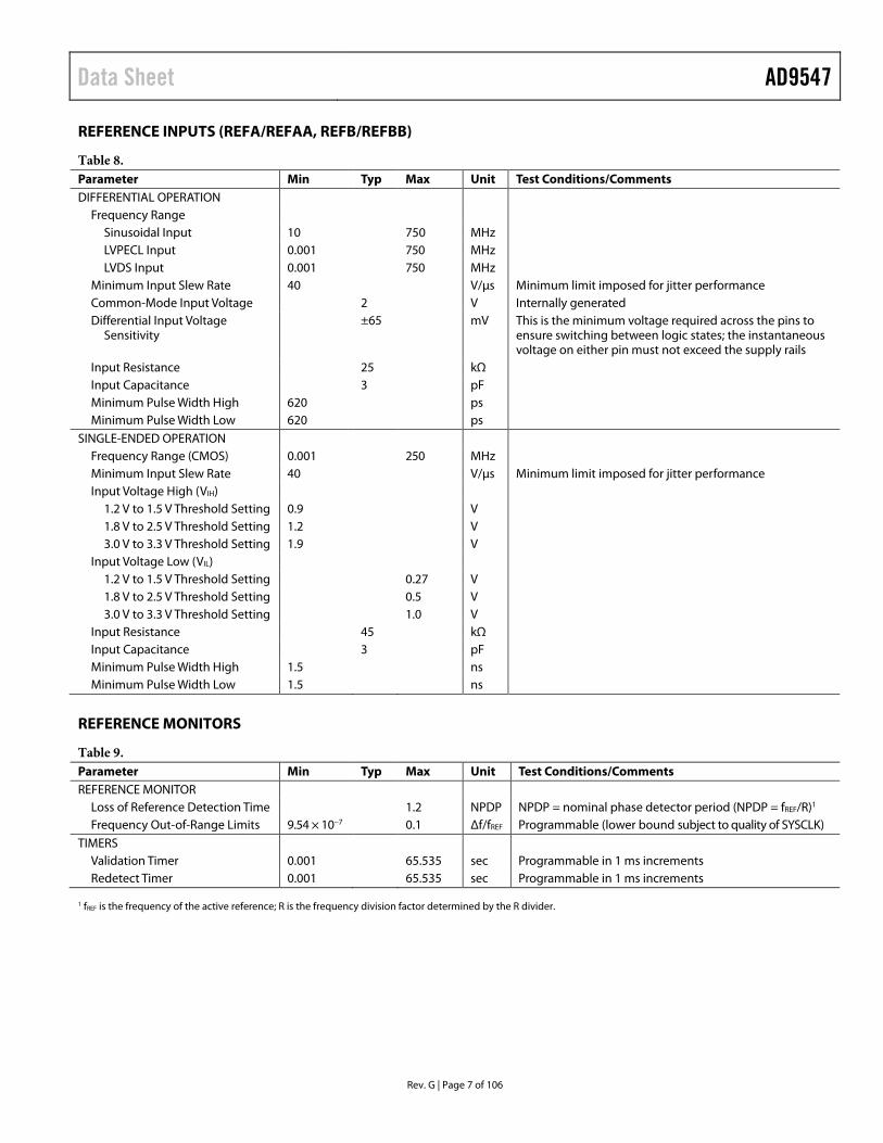
REFERENCE MONITORS
Table 9. Parameter Min Typ Max Unit Test Conditions/Comments REFERENCE MONITOR
Loss of Reference Detection Time 1.2 NPDP NPDP = nominal phase detector period (NPDP = fREF/R)1 Frequency Out-of-Range Limits 9.54 × 10⁻⁷ 0.1 Δf/fREF Programmable (lower bound subject to quality of SYSCLK)
TIMERS Validation Timer 0.001 65.535 sec Programmable in 1 ms increments Redetect Timer 0.001 65.535 sec Programmable in 1 ms increments
1 fREF is the frequency of the active reference; R is the frequency division factor determined by the R divider.
Rev. G | Page 7 of 106

AD9547 Data Sheet
REFERENCE SWITCHOVER SPECIFICATIONS
Table 10. Parameter Min Typ Max Unit Test Conditions/Comments MAXIMUM OUTPUT PHASE
PERTURBATION (PHASE BUILD-OUT SWITCHOVER)
40 200 ps Assumes a jitter-free reference; satisfies Telcordia GR-1244-CORE requirements
MAXIMUM TIME/TIME SLOPE (HITLESS SWITCHOVER)
315 65,535 ns/sec Minimum/maximum values are program-mable upper bounds; a minimum value ensures <10% error; satisfies Telcordia GR-1244-CORE requirements
TIME REQUIRED TO SWITCH TO A NEW REFERENCE
Hitless Switchover 5 NPDP NPDP = nominal phase detector period (NPDP = fREF/R)1
Phase Build-Out Switchover 3 NPDP NPDP = nominal phase detector period (NPDP = fREF/R)1
1 fREF is the frequency of the active reference; R is the frequency division factor determined by the R divider.
DISTRIBUTION CLOCK OUTPUTS (OUT0, OUT1)
Table 11. Parameter Min Typ Max Unit Test Conditions/Comments LVPECL MODE Using internal current setting resistor
(nominal 3.12 kΩ) Maximum Output Frequency 725 MHz Rise/Fall Time1 (20% to 80%) 180 315 ps 100 Ω termination across output pins Duty Cycle 45 55 % Differential Output Voltage Swing 630 770 910 mV Magnitude of voltage across pins; output
driver static Common-Mode Output Voltage AVDD3 − 1.5 AVDD3 − 1.3 AVDD3 − 1.05 V Output driver static
LVDS MODE Using internal current setting resistor (nominal 3.12 kΩ)
Maximum Output Frequency 725 MHz Rise/Fall Time1 (20% to 80%) 200 350 ps 100 Ω termination across the output pins Duty Cycle 40 60 % Differential Output Voltage Swing
Balanced (VOD) 247 454 mV Voltage swing between output pins; output driver static
Unbalanced (ΔVOD) 50 mV Absolute difference between voltage swing of normal pin and inverted pin; output driver static
Offset Voltage Common Mode (VOS) 1.125 1.375 V Output driver static Common-Mode Difference (ΔVOS) 50 mV Voltage difference between pins; output
driver static Short-Circuit Output Current 13 24 mA Output driver static
CMOS MODE Weak drive option not supported for operating the CMOS drivers using a 1.8 V supply
Maximum Output Frequency 3.3 V Supply 10 pF load
Strong Drive Strength Setting 250 MHz Weak Drive Strength Setting 25 MHz
1.8 V Supply 150 MHz
Rev. G | Page 8 of 106

Data Sheet AD9547
Parameter Min Typ Max Unit Test Conditions/Comments Rise/Fall Time1 (20% to 80%) 10 pF load
3.3 V Supply Strong Drive Strength Setting 0.5 2 ns Weak Drive Strength Setting 8 14.5 ns
1.8 V Supply 1.5 2.5 ns Duty Cycle 40 60 % 10 pF load Output Voltage High (VOH) Output driver static; strong drive
strength setting AVDD3 = 3.3 V, IOH = 10 mA 2.6 V AVDD3 = 3.3 V, IOH = 1 mA 2.9 V AVDD3 = 1.8 V, IOH = 1 mA 1.5 V
Output Voltage Low (VOL) Output driver static; strong drive strength setting
AVDD3 = 3.3 V, IOL = 10 mA 0.3 V AVDD3 = 3.3 V, IOL = 1 mA 0.1 V AVDD3 = 1.8 V, IOL = 1 mA 0.1 V
OUTPUT TIMING SKEW 10 pF load Between LVPECL Outputs 14 125 ps Rising edge only; any divide value Between LVDS Outputs 13 138 ps Rising edge only; any divide value Between CMOS (3.3 V) Outputs
Strong Drive Strength Setting 23 240 ps Weak Drive Strength Setting 24 ps
Between CMOS (1.8 V) Outputs 40 ps Weak drive option not supported at 1.8 V Between LVPECL Outputs and LVDS
Outputs 14 140 ps
Between LVPECL Outputs and CMOS Outputs
19 ps
ZERO-DELAY TIMING SKEW ±5 ns Output relative to active input reference; output distribution synchronization to active reference feature enabled; assumes manual phase offset compensation of deterministic latency
1 The listed values are for the slower edge (rising or falling).
DAC OUTPUT CHARACTERISTICS (DACOUTP, DACOUTN)
Table 12. Parameter Min Typ Max Unit Test Conditions/Comments FREQUENCY RANGE 62.5 450 MHz OUTPUT OFFSET VOLTAGE 15 mV This is the single-ended voltage at either
DAC output pin (no external load) when the internal DAC code is such that no current is delivered to that pin
VOLTAGE COMPLIANCE RANGE VSS − 0.5 0.5 VSS + 0.5 V OUTPUT RESISTANCE 50 Ω Single-ended; each pin has an internal
50 Ω termination to VSS OUTPUT CAPACITANCE 5 pF FULL-SCALE OUTPUT CURRENT 20 mA Programmable (8 mA to 31 mA; see the
DAC Output section) GAIN ERROR −12 +12 % FS
Rev. G | Page 9 of 106

AD9547 Data Sheet
TIME DURATION OF DIGITAL FUNCTIONS
Table 13. Parameter Min Typ Max Unit Test Conditions/Comments EEPROM-TO-REGISTER DOWNLOAD TIME 25 ms Using default EEPROM storage sequence
(see Register 0x0E10 to Register 0x0E3F) REGISTER-TO-EEPROM UPLOAD TIME 200 ms Using default EEPROM storage sequence
(see Register 0x0E10 to Register 0x0E3F) MINIMUM POWER-DOWN EXIT TIME 10.5 µs Dependent on loop filter bandwidth MAXIMUM TIME FROM ASSERTION OF THE RESET PIN
TO THE M0 TO M7 PINS ENTERING HIGH IMPEDANCE STATE
45 ns
DIGITAL PLL
Table 14. Parameter Min Typ Max Unit Test Conditions/Comments PHASE FREQUENCY DETECTOR (PFD) INPUT
FREQUENCY RANGE 0.001 10 MHz Maximum fPFD = fS/1001, 2
LOOP BANDWIDTH 0.001 1 × 10⁵ Hz Programmable design parameter; maximum fLOOP = fREF/(20R)3
PHASE MARGIN 30 89 Degrees Programmable design parameter REFERENCE INPUT (R) DIVISION FACTOR 1 230 1, 2, …1,073,741,824 INTEGER FEEDBACK (S) DIVISION FACTOR 8 220 8, 9, …1,048,576 FRACTIONAL FEEDBACK DIVIDE RATIO 0 0.999 Maximum value = 1022/1023
1 fPFD is the frequency at the input to the phase-frequency detector. 2 fS is the sample rate of the output DAC. 3 fREF is the frequency of the active reference; R is the frequency division factor determined by the R divider.
DIGITAL PLL LOCK DETECTION
Table 15. Parameter Min Typ Max Unit Test Conditions/Comments PHASE LOCK DETECTOR
Threshold Programming Range 0.001 65.5 ns Threshold Resolution 1 ps
FREQUENCY LOCK DETECTOR Threshold Programming Range 0.001 16,700 ns Reference-to-feedback period difference Threshold Resolution 1 ps
HOLDOVER SPECIFICATIONS
Table 16. Parameter Min Typ Max Unit Test Conditions/Comments FREQUENCY ACCURACY <0.01 ppb Excludes frequency drift of SYSCLK source;
excludes frequency drift of input reference prior to entering holdover
Rev. G | Page 10 of 106

Data Sheet AD9547
SERIAL PORT SPECIFICATIONS—SPI MODE
Table 17. Parameter Min Typ Max Unit Test Conditions/Comments CS Internal 30 kΩ pull-up resistor
Input Logic 1 Voltage 2.0 V Input Logic 0 Voltage 0.8 V Input Logic 1 Current 30 µA Input Logic 0 Current 110 µA Input Capacitance 2 pF
SCLK Internal 30 kΩ pull-down resistor Input Logic 1 Voltage 2.0 V Input Logic 0 Voltage 0.8 V Input Logic 1 Current 1 µA Input Logic 0 Current 1 µA Input Capacitance 2 pF
SDIO As an Input
Input Logic 1 Voltage 2.0 V Input Logic 0 Voltage 0.8 V Input Logic 1 Current 1 µA Input Logic 0 Current 1 µA Input Capacitance 2 pF
As an Output Output Logic 1 Voltage 2.7 V 1 mA load current Output Logic 0 Voltage 0.4 V 1 mA load current
SDO Output Logic 1 Voltage 2.7 V 1 mA load current Output Logic 0 Voltage 0.4 V 1 mA load current
TIMING SCLK
Clock Rate, 1/tCLK 40 MHz Pulse Width High, tHIGH 10 ns Pulse Width Low, tLOW 12 ns
SDIO to SCLK Setup, tDS 3 ns SCLK to SDIO Hold, tDH 0 ns SCLK to Valid SDIO and SDO, tDV 15 ns CS to SCLK Setup, tS 10 ns
CS to SCLK Hold, tC 0 ns
CS Minimum Pulse Width High 6 ns
Rev. G | Page 11 of 106

AD9547 Data Sheet
SERIAL PORT SPECIFICATIONS—I2C MODE
Table 18. Parameter Min Typ Max Unit Test Conditions/Comments SDA (AS INPUT), SCL No internal pull-up/pull-down
resistor Input Logic 1 Voltage 0.7 × DVDD3 V Input Logic 0 Voltage 0.3 × DVDD3 V Input Current −10 +10 µA For VIN = 10% to 90% of DVDD3 Hysteresis of Schmitt Trigger Inputs 0.015 × DVDD3 V Pulse Width of Spikes That Must Be
Suppressed by the Input Filter, tSP 50 ns
SDA (AS OUTPUT) Output Logic 0 Voltage 0.4 V IO = 3 mA Output Fall Time from VIHmin to VILmax 20 + 0.1 Cb
1 250 ns 10 pF ≤ Cb ≤ 400 pF TIMING
SCL Clock Rate 400 kHz Bus Free Time Between a Stop and Start
Condition, tBUF 1.3 µs
Repeated Start Condition Setup Time, tSU;STA 0.6 µs Repeated Hold Time Start Condition, tHD;STA 0.6 µs After this period, the first clock
pulse is generated Stop Condition Setup Time, tSU;STO 0.6 µs Low Period of the SCL Clock, tLOW 1.3 µs High Period of the SCL Clock, tHIGH 0.6 µs SCL/SDA Rise Time, tR
20 + 0.1 Cb1 300 ns
SCL/SDA Fall Time, tF 20 + 0.1 Cb1 300 ns
Data Setup Time, tSU;DAT 100 ns Data Hold Time, tHD;DAT 100 ns Capacitive Load for Each Bus Line, Cb
1 400 pF
1 Cb is the capacitance (pF) of a single bus line.
Rev. G | Page 12 of 106

Data Sheet AD9547
JITTER GENERATION
Table 19. Parameter Min Typ Max Unit Test Conditions/Comments CONDITIONS: fREF = 8 kHz1, fDDS = 155.52 MHz2,
fLOOP = 100 Hz3 fSYSCLK = 50 MHz4 crystal; fS = 1 GHz5;
Q-divider = 1; default SYSCLK PLL charge pump current; results valid for LVPECL, LVDS, and CMOS output logic types
Bandwidth: 100 Hz to 77 MHz 0.71 ps rms Random jitter Bandwidth: 5 kHz to 20 MHz 0.34 ps rms Random jitter Bandwidth: 20 kHz to 80 MHz 0.43 ps rms Random jitter Bandwidth: 50 kHz to 80 MHz 0.43 ps rms Random jitter Bandwidth: 4 MHz to 80 MHz 0.31 ps rms Random jitter
CONDITIONS: fREF = 19.44 MHz1, fDDS = 155.52 MHz2, fLOOP = 1 kHz3
fSYSCLK = 50 MHz4 crystal; fS = 1 GHz5; Q-divider = 1; default SYSCLK PLL charge pump current; results valid for LVPECL, LVDS, and CMOS output logic types
Bandwidth: 100 Hz to 77 MHz 1.05 ps rms Random jitter Bandwidth: 5 kHz to 20 MHz 0.34 ps rms Random jitter Bandwidth: 20 kHz to 80 MHz 0.43 ps rms Random jitter Bandwidth: 50 kHz to 80 MHz 0.43 ps rms Random jitter Bandwidth: 4 MHz to 80 MHz 0.32 ps rms Random jitter
CONDITIONS: fREF = 19.44 MHz1, fDDS = 311.04 MHz2, fLOOP = 1 kHz3
fSYSCLK = 50 MHz4 crystal; fS = 1 GHz5; Q-divider = 1; default SYSCLK PLL charge pump current; results valid for LVPECL, LVDS, and CMOS output logic types
Bandwidth: 100 Hz to 100 MHz 0.67 ps rms Random jitter Bandwidth: 5 kHz to 20 MHz 0.31 ps rms Random jitter Bandwidth: 20 kHz to 80 MHz 0.33 ps rms Random jitter Bandwidth: 50 kHz to 80 MHz 0.33 ps rms Random jitter Bandwidth: 4 MHz to 80 MHz 0.16 ps rms Random jitter
1 fREF is the frequency of the active reference. 2 fDDS is the output frequency of the DDS. 3 fLOOP is the DPLL digital loop filter bandwidth. 4 fSYSCLK is the frequency at the SYSCLKP and SYSCLKN pins. 5 fS is the sample rate of the output DAC.
Rev. G | Page 13 of 106

AD9547 Data Sheet
ABSOLUTE MAXIMUM RATINGS Table 20. Parameter Rating Analog Supply Voltage (AVDD) 2 V Digital Supply Voltage (DVDD) 2 V Digital I/O Supply Voltage (DVDD3) 3.6 V DAC Supply Voltage (AVDD3) 3.6 V Maximum Digital Input Voltage −0.5 V to DVDD3 + 0.5 V Storage Temperature Range −65°C to +150°C Operating Temperature Range −40°C to +85°C Lead Temperature
(Soldering 10 sec) 300°C
Junction Temperature 150°C
Stresses at or above those listed under Absolute Maximum Ratings may cause permanent damage to the product. This is a stress rating only; functional operation of the product at these or any other conditions above those indicated in the operational section of this specification is not implied. Operation beyond the maximum operating conditions for extended periods may affect product reliability.
ESD CAUTION
Rev. G | Page 14 of 106
Data Sheet AD9547
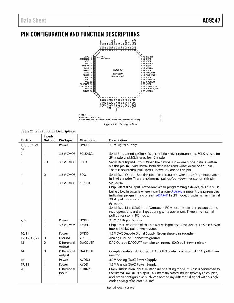
PIN CONFIGURATION AND FUNCTION DESCRIPTIONS
PIN 1INDICATOR
17 18 19 20 21 22 23 24 25 26 27 28 29 30 31 32
AVD
DAV
DD
VSS
CLK
INN
CLK
INP
VSS
AVD
DO
UT_
RSE
TAV
DD
3O
UT0
PO
UT0
NAV
DD
OU
T1P
OU
T1N
AVD
D3
AVD
D
64 63 62 61 60 59 58 57 56 55 54 53 52 51 50 49
DVD
DM
7M
6M
5M
4D
VDD
DVD
D3
M3
M2
M1
M0
DVD
DIR
QN
CAV
DD
AVD
D3
123456789
10111213141516
DVDDSCLK/SCL
SDIOSDO
CS/SDADVDD
DVDD3DVDD
RESETDVDDDVDD
VSSDACOUTPDACOUTN
VSSAVDD3
NOTES1. NC = NO CONNECT.2. THE EXPOSED PAD MUST BE CONNECTED TO GROUND (VSS).
REFBBREFBAVDDREFAAREFAAVDD3AVDDTDC_VRTTDC_VRBAVDDSYSCLKPSYSCLKNAVDDSYSCLK_LFSYSCLK_VREGAVDD3
48474645444342414039383736353433
AD9547TOP VIEW
(Not to Scale)
0830
0-00
2
Figure 2. Pin Configuration
Table 21. Pin Function Descriptions
Pin No. Input/ Output Pin Type Mnemonic Description
1, 6, 8, 53, 59, 64
I Power DVDD 1.8 V Digital Supply.
2 I 3.3 V CMOS SCLK/SCL Serial Programming Clock. Data clock for serial programming. SCLK is used for SPI mode, and SCL is used for I2C mode.
3 I/O 3.3 V CMOS SDIO Serial Data Input/Output. When the device is in 4-wire mode, data is written via this pin. In 3-wire mode, both data reads and writes occur on this pin. There is no internal pull-up/pull-down resistor on this pin.
4 O 3.3 V CMOS SDO Serial Data Output. Use this pin to read data in 4-wire mode (high impedance in 3-wire mode). There is no internal pull-up/pull-down resistor on this pin.
5 I 3.3 V CMOS CS/SDA SPI Mode. Chip Select (CS) Input. Active low. When programming a device, this pin must be held low. In systems where more than one AD9547 is present, this pin enables individual programming of each AD9547. In SPI mode, this pin has an internal 30 kΩ pull-up resistor.
I2C Mode. Serial Data Line (SDA) Input/Output. In I2C Mode, this pin is an output during read operations and an input during write operations. There is no internal pull-up resistor in I2C mode.
7, 58 I Power DVDD3 3.3 V I/O Digital Supply. 9 I 3.3 V CMOS RESET Chip Reset. Assertion of this pin (active high) resets the device. This pin has an
internal 50 kΩ pull-down resistor. 10, 11 I Power DVDD 1.8 V DAC Decode Digital Supply. Group these pins together. 12, 15, 19, 22 O Ground VSS Analog Ground. Connect to ground. 13 O Differential
output DACOUTP DAC Output. DACOUTP contains an internal 50 Ω pull-down resistor.
14 O Differential output
DACOUTN Complementary DAC Output. DACOUTN contains an internal 50 Ω pull-down resistor.
16 I Power AVDD3 3.3 V Analog (DAC) Power Supply. 17, 18 I Power AVDD 1.8 V Analog (DAC) Power Supply. 20 I Differential
input CLKINN Clock Distribution Input. In standard operating mode, this pin is connected to
the filtered DACOUTN output. This internally biased input is typically ac-coupled, and, when configured as such, can accept any differential signal with a single-ended swing of at least 400 mV.
Rev. G | Page 15 of 106
AD9547 Data Sheet
Pin No. Input/ Output Pin Type Mnemonic Description
21 I Differential input
CLKINP Clock Distribution Input. In standard operating mode, this pin is connected to the filtered DACOUTP output.
23 I Power AVDD 1.8 V Analog (Input Receiver) Power Supply. 24 O Current set
resistor OUT_RSET Connect an optional 3.12 kΩ resistor from this pin to ground (see the Output
Current Control with an External Resistor section). 25, 31 I Power AVDD3 Analog Supply for Output Driver. These pins are normally 3.3 V but can be
1.8 V. Pin 25 powers OUT0. Pin 31 powers OUT1. Apply power to these pins even if the corresponding outputs (OUT0P/OUT0N, OUT1P/OUT1N) are not used. See the Power Supply Partitions section.
26 O LVPECL, LVDS, or CMOS
OUT0P Output 0. This output can be configured as LVPECL, LVDS, or single-ended CMOS. LVPECL and LVDS operation require a 3.3 V output driver power supply. CMOS operation can be either 1.8 V or 3.3 V, depending on the output driver power supply.
27 O LVPECL, LVDS, or CMOS
OUT0N Complementary Output 0. This output can be configured as LVPECL, LVDS, or single-ended CMOS.
28, 32 I Power AVDD 1.8 V Analog (Output Divider) Power Supply. 29 O LVPECL,
LVDS, or CMOS
OUT1P Output 1. This output can be configured as LVPECL, LVDS, or single-ended CMOS. LVPECL and LVDS operation require a 3.3 V output driver power supply. CMOS operation can be either 1.8 V or 3.3 V, depending on the output driver power supply.
30 O LVPECL, LVDS, or CMOS
OUT1N Complementary Output 1. This output can be configured as LVPECL, LVDS, or single-ended CMOS.
33 I Power AVDD3 3.3 V Analog (System Clock) Power Supply. 34 I SYSCLK_VREG System Clock Loop Filter Voltage Regulator. Connect a 0.1 µF capacitor from
this pin to ground. This pin is also the ac ground reference for the integrated external loop filter of the SYSCLK PLL multiplier (see the SYSCLK PLL Multiplier section).
35 O SYSCLK_LF System Clock Multiplier Loop Filter. When using the frequency multiplier to drive the system clock, an external loop filter can be attached to this pin.
36, 39 I Power AVDD 1.8 V Analog (System Clock) Power Supply. 37 I Differential
input SYSCLKN Complementary System Clock Input. Complementary signal to SYSCLKP.
SYSCLKN contains internal dc biasing and should be ac-coupled with a 0.01 µF capacitor, except when using a crystal. When using a crystal, connect the crystal across SYSCLKP and SYSCLKN. In crystal mode, the user should consider placing a 0 Ω series resistor on the SYSCLKN pin. In the event that the power dissipated in the crystal must be reduced, the user can replace the 0 Ω resistor with a larger resistor (for example, 500 Ω). However, this series resistor is rarely needed. (See Figure 32).
38 I Differential input
SYSCLKP System Clock Input. SYSCLKP contains internal dc biasing and should be ac-coupled with a 0.01 µF capacitor, except when using a crystal. When using a crystal, connect it directly across SYSCLKP and SYSCLKN. Single-ended 1.8 V CMOS is also an option but can introduce a spur if the doubler is enabled and the duty cycle is not 50%. When using SYSCLKP as a single-ended input, connect a 0.01 µF capacitor from SYSCLKN to ground.
40, 41 I TDC_VRB, TDC_VRT
Use capacitive decoupling on these pins (see Figure 38).
42 I Power AVDD 1.8 V Analog (Time-to-Digital Converter) Power Supply. 43, 49 I Power AVDD3 3.3 V Analog (Reference Input) Power Supply. 44 I Differential
input REFA Reference A Input. This internally biased input is typically ac-coupled and,
when configured as such, can accept any differential signal with a single-ended swing of up to 3.3 V. If dc-coupled, input can be LVPECL, CMOS, or LVDS.
45 I Differential input
REFAA Complementary Reference A Input. Complementary signal to the input pro-vided on Pin 44. The user can configure this pin as a separate single-ended input.
46, 50 I Power AVDD 1.8 V Analog (Reference Input) Power Supply.
Rev. G | Page 16 of 106
Data Sheet AD9547
Pin No. Input/ Output Pin Type Mnemonic Description
47 I Differential input
REFB Reference B Input. This internally biased input is typically ac-coupled and, when configured as such, can accept any differential signal with a single-ended swing of up to 3.3 V. If dc-coupled, input can be LVPECL, CMOS, or LVDS.
48 I Differential input
REFBB Complementary Reference B Input. Complementary signal to the input provided on Pin 47. The user can configure this pin as a separate single-ended input.
51 I NC No Connection. This pin should be left floating. 52 O Logic IRQ Interrupt Request Line. 54, 55, 56, 57, 60, 61, 62, 63
I/O 3.3 V CMOS M0, M1, M2, M3, M4, M5, M6, M7
Configurable I/O Pins. These pins are configured under program control. M0 to M2 control the serial port mode selection (see Table 30), and M3 to M7 control the EEPROM loading at startup or reset (see the Initial M0 to M7 Pin Programming section). Note that there are no internal pull-up or pull-down resistors on these pins, and the user should place pull-up or pull-down resistors on each of these pins to avoid unpredictable start-up behavior.
EP O Exposed pad
Exposed pad The exposed pad must be connected to ground (VSS).
Rev. G | Page 17 of 106
AD9547 Data Sheet
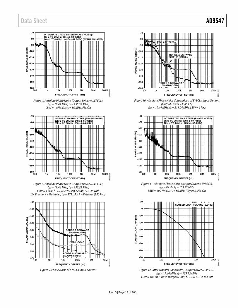
TYPICAL PERFORMANCE CHARACTERISTICS fREF = input reference clock frequency, fO = clock frequency, fSYSCLK = SYSCLK input frequency, fS =internal system clock frequency, LBW = DPLL loop bandwidth, PLL off = SYSCLK PLL bypassed, PLL on = SYSCLK PLL enabled, ICP = SYSCLK PLL charge pump current, LF = SYSCLK PLL loop filter. AVDD, AVDD3, and DVDD at nominal supply voltage, fS = 1 GHz, ICP = automatic mode, LF = internal, unless otherwise noted.
–160
–150
–140
–130
–120
–110
–100
–90
–80
–70
100 1k 10k 100k 1M 10M 100M
PHA
SE N
OIS
E (d
Bc/
Hz)
FREQUENCY OFFSET (Hz)
INTEGRATED RMS JITTER (PHASE NOISE):5kHz TO 20MHz: 173fs (–75.4dBc)20kHz TO 80MHz: 315fs (–70.2dBc) (EXTRAPOLATED)
0830
0-06
8
Figure 3. Absolute Phase Noise (Output Driver = LVPECL),
fREF = 19.44 MHz, fO = 155.52 MHz, LBW = 1 kHz, fSYSCLK = 1 GHz, PLL Off
–160
–150
–140
–130
–120
–110
–100
–90
–80
–70
100 1k 10k 100k 1M 10M 100M
PHA
SE N
OIS
E (d
Bc/
Hz)
FREQUENCY OFFSET (Hz)
INTEGRATED RMS JITTER (PHASE NOISE):5kHz TO 20MHz: 333fs (–69.8dBc)20kHz TO 80MHz: 430fs (–67.6dBc) (EXTRAPOLATED)
0830
0-05
6
Figure 4. Absolute Phase Noise (Output Driver = LVPECL), fREF = 19.44 MHz, fO = 155.52 MHz,
LBW = 1 kHz, fSYSCLK = 50 MHz (Crystal), PLL On
–160
–150
–140
–130
–120
–110
–100
–90
–80
–70
100 1k 10k 100k 1M 10M 100M
PHA
SE N
OIS
E (d
Bc/
Hz)
FREQUENCY OFFSET (Hz)
INTEGRATED RMS JITTER (PHASE NOISE):5kHz TO 20MHz: 103fs (–74.0dBc)20kHz TO 80MHz: 160fs (–70.1dBc)
0830
0-06
6
Figure 5. Absolute Phase Noise (Output Driver = LVPECL),
fREF = 19.44 MHz, fO = 311.04 MHz, LBW = 1 kHz, fSYSCLK = 1 GHz, PLL Off
–160
–150
–140
–130
–120
–110
–100
–90
–80
–70
100 1k 10k 100k 1M 10M 100M
PHA
SE N
OIS
E (d
Bc/
Hz)
FREQUENCY OFFSET (Hz)
INTEGRATED RMS JITTER (PHASE NOISE):5kHz TO 20MHz: 310fs (–64.4dBc)20kHz TO 80MHz: 330fs (–63.9dBc)
0830
0-06
7
Figure 6. Absolute Phase Noise (Output Driver = LVPECL), fREF = 19.44 MHz, fO = 311.04 MHz,
LBW = 1 kHz, fSYSCLK = 50 MHz (Crystal), PLL On
Rev. G | Page 18 of 106
Data Sheet AD9547
–160
–150
–140
–130
–120
–110
–100
–90
–80
–70
100 1k 10k 100k 1M 10M 100M
PHA
SE N
OIS
E (d
Bc/
Hz)
FREQUENCY OFFSET (Hz)
INTEGRATED RMS JITTER (PHASE NOISE):5kHz TO 20MHz: 361fs (–69.0dBc)20kHz TO 80MHz: 441fs (–67.3dBc) (EXTRAPOLATED)
0830
0-06
9
Figure 7. Absolute Phase Noise (Output Driver = LVPECL),
fREF = 19.44 MHz, fO = 155.52 MHz, LBW = 1 kHz, fSYSCLK = 50 MHz, PLL On
–160
–150
–140
–130
–120
–110
–100
–90
–80
–70
100 1k 10k 100k 1M 10M 100M
PHA
SE N
OIS
E (d
Bc/
Hz)
FREQUENCY OFFSET (Hz)
INTEGRATED RMS JITTER (PHASE NOISE):12kHz TO 20MHz: 245fs (–65.0dBc)20kHz TO 80MHz: 300fs (–64.3dBc)
0830
0-05
1
Figure 8. Absolute Phase Noise (Output Driver = LVPECL),
fREF = 19.44 MHz, fO = 155.52 MHz, LBW = 1 kHz, fSYSCLK = 50 MHz (Crystal), PLL On with
2× Frequency Multiplier, ICP = 375 µA, LF = External (350 kHz)
ROHDE & SCHWARZSMA100 (1GHz)
ROHDE & SCHWARZSMA100 (50MHz)
20MHz OCXO
–170
–160
–150
–140
–130
–120
–110
–100
–90
100 1k 10k 100k 1M 10M
PHA
SE N
OIS
E (d
Bc/
Hz)
FREQUENCY OFFSET (Hz)
0830
0-05
3
Figure 9. Phase Noise of SYSCLK Input Sources
–160
–150
–140
–130
–120
–110
–100
–90
–80
–70
100 1k 10k 100k 1M 10M 100M
PHA
SE N
OIS
E (d
Bc/
Hz)
FREQUENCY OFFSET (Hz)
ROHDE & SCHWARZSMA100 (1GHz)
ROHDE & SCHWARZSMA100 (50MHz)
50MHz CRYSTAL
0830
0-05
8
Figure 10. Absolute Phase Noise Comparison of SYSCLK Input Options
(Output Driver = LVPECL), fREF = 19.44 MHz, fO = 311.04 MHz, LBW = 1 kHz
100 1k 10k 100k 1M 10M 100M
PHA
SE N
OIS
E (d
Bc/
Hz)
FREQUENCY OFFSET (Hz)
–160
–150
–140
–130
–120
–110
–100
–90
–80
–70INTEGRATED RMS JITTER (PHASE NOISE):5kHz TO 20MHz: 336fs (–69.7dBc)20kHz TO 80MHz: 425fs (–67.6dBc)
0830
0-05
2
Figure 11. Absolute Phase Noise (Output Driver = LVPECL),
fREF = 8 kHz, fO = 155.52 MHz, LBW = 100 Hz, fSYSCLK = 50 MHz (Crystal), PLL On
–70
–60
–50
–40
–30
–20
–10
0
10
10 100 1k 10k 100k
FREQUENCY OFFSET (Hz)
CLO
SED
-LO
OP
GA
IN (d
B)
CLOSED-LOOP PEAKING: 0.04dB
0830
0-04
7
Figure 12. Jitter Transfer Bandwidth, Output Driver = LVPECL,
fREF = 19.44 MHz, fO = 155.52 MHz, LBW = 100 Hz (Phase Margin = 88°), fSYSCLK = 1 GHz, PLL Off
Rev. G | Page 19 of 106

AD9547 Data Sheet
LVDS
0
0.2
0.4
0.6
0.8
1.0
0 100 200 300 400 500 600 700
AM
PLIT
UD
E (V
)
FREQUENCY (MHz)
LVPECL
0830
0-04
9
Figure 13. Amplitude vs. Toggle Rate,
LVPECL and LVDS
10pF LOAD
20pF LOAD
1.0
1.5
2.0
2.5
3.0
3.5
4.0
0 100 200 300 400 500
AM
PLIT
UD
E (V
)
FREQUENCY (MHz)
0830
0-05
5
Figure 14. Amplitude vs. Toggle Rate, 3.3 V CMOS (Strong Mode)
LVDS
LVPECL
50
60
70
80
120
110
100
90
130
140
0 100 200 300 400 500
POW
ER (m
W)
FREQUENCY (MHz)
0830
0-06
4
Figure 15. Power Consumption vs. Frequency, LVPECL and LVDS (Single Channel)
AM
PLIT
UD
E (V
)
FREQUENCY (MHz)
0.5
1.0
1.5
2.0
0 50 100 150 250200
5pF LOAD
10pF LOAD
20pF LOAD
0830
0-06
2
Figure 16. Amplitude vs. Toggle Rate,
1.8 V CMOS
10pF LOAD
5pF LOAD
1.0
1.5
2.0
2.5
3.0
3.5
4.0
0 10 20 30 40 50
AM
PLIT
UD
E (V
)
FREQUENCY (MHz)
0830
0-06
3
Figure 17. Amplitude vs. Toggle Rate, 3.3 V CMOS (Weak Mode)
POW
ER (m
W)
FREQUENCY (MHz)
15
20
25
30
35
40
0 50 100 150 200
10pF LOAD 5pF LOAD
20pF LOAD
0830
0-06
1
Figure 18. Power Consumption vs. Frequency, 1.8 V CMOS
Rev. G | Page 20 of 106

Data Sheet AD9547
20
40
60
80
100
120
140
160
0 50 100 150 200 250 300 350
POW
ER (m
W)
FREQUENCY (MHz)
10pF LOAD 5pF LOAD
20pF LOAD
0830
0-06
0
Figure 19. Power Consumption vs. Frequency, 3.3 V CMOS (Strong Mode)
–1.0
–0.8
–0.6
–0.4
–0.2
0
0.2
0.4
0.6
0.8
1.0
0 1 2 3 4 5
DIF
FER
ENTI
ALA
MPL
ITU
DE
(V)
TIME (ns)
0830
0-05
0
Figure 20. Output Waveform, LVPECL (400 MHz)
–0.5
0
0.5
1.0
1.5
2.0
2.5
3.0
3.5
0 2 4 6 8 10 12 14 16
AM
PLIT
UD
E (V
)
TIME (ns)
20pF LOAD
10pF LOAD
0830
0-05
7
Figure 21. Output Waveform, 3.3 V CMOS (100 MHz, Strong Mode)
20pF LOAD 5pF LOAD
20
22
24
26
28
30
32
34
10 15 20 25 30 35 40
POW
ER (m
W)
FREQUENCY (MHz)
10pF LOAD
0830
0-05
9
Figure 22. Power Consumption vs. Frequency, 3.3 V CMOS (Weak Mode)
–0.5
–0.4
–0.3
–0.2
–0.1
0
0.1
0.2
0.3
0.4
0.5
0 1 2 3 4 5
DIF
FER
ENTI
ALA
MPL
ITU
DE
(V)
TIME (ns)
0830
0-04
8
Figure 23. Output Waveform, LVDS (400 MHz)
5pF LOAD
20 pF LOAD
–0.5
0
0.5
1.0
1.5
2.0
2.5
3.0
3.5
0 10 20 30 40 50 60 70 80
AM
PLIT
UD
E (V
)
TIME (ns)
0830
0-04
6
Figure 24. Output Waveform, 3.3 V CMOS (20 MHz, Weak Mode)
Rev. G | Page 21 of 106
AD9547 Data Sheet
–0.5
0
0.5
1.0
1.5
2.0
0 2 4 6 8 10 12 14 16
AM
PLIT
UD
E (V
)
TIME (ns)
20pF LOAD
10pF LOAD
0830
0-06
5
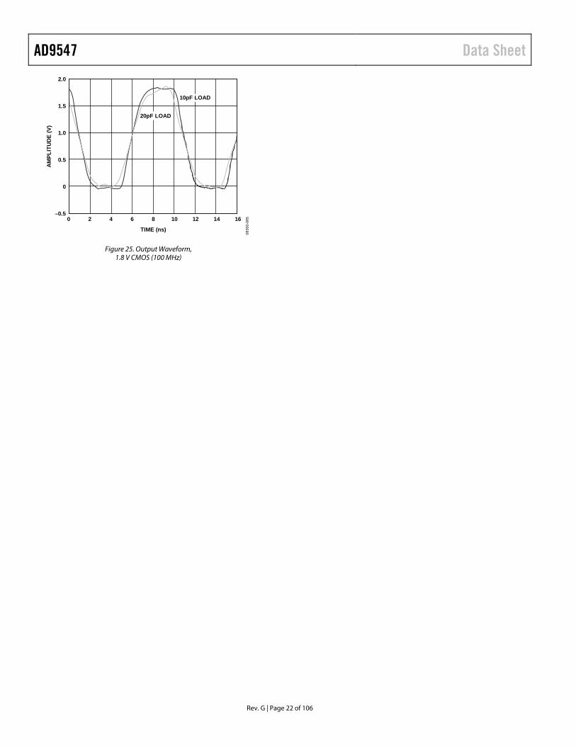
Figure 25. Output Waveform, 1.8 V CMOS (100 MHz)
Rev. G | Page 22 of 106
Data Sheet AD9547
INPUT/OUTPUT TERMINATION RECOMMENDATIONS
AD9547
100Ω
HIGHIMPEDANCE
INPUTDOWNSTREAM
DEVICE
0.1µF
0.1µF
3.3V LVDSOUTPUT
0830
0-00
3
Figure 26. AC-Coupled LVDS or LVPECL Output Driver
AD9547
100Ω DOWNSTREAM
DEVICE3.3VLVPECL-
COMPATIBLEOUTPUT
0830
0-00
4
Figure 27. DC-Coupled LVDS or LVPECL Output Driver
0.1µF
0.1µF
AD9547SELF-BIASEDREFERENCE
INPUT(OPT
ION
AL)
100Ω
0830
0-00
5
Figure 28. Reference Input
0.1µF
0.1µF
AD9547SELF-BIASED
SYSCLKxINPUT(O
PTIO
NA
L)
100Ω
0830
0-00
6
Figure 29. SYSCLKx Input
0.1µF
0.1µF
AD9547SELF-BIASED
CLKINxINPUT(O
PTIO
NA
L)
100Ω
0830
0-00
7
Figure 30. CLKINx Input
SYSCLKP300Ω
150Ω
0.1µF
SYSCLKN
AD9547
3.3VCMOSTCXO
0.1µF
0830
0-13
4
Figure 31. System Clock Input (SYSCLKP/SYSCLKN) When Using a
TCXO/OCXO with 3.3 V CMOS Output
0830
0-13
3
SYSCLKP
SYSCLKN
AD954710MHz TO 50MHz FUNDAMENTALAT-CUT CRYSTAL WITH 10pFLOAD CAPACITANCE (CLOAD)
15pF
15pF 0Ω(OPTIONAL)
NOTES1. THE RECOMMENDED CLOAD = 10pF IS SHOWN. THE VALUES OF THE 15pF SHUNT CAPACITORS SHOWN HERE MUST EQUAL 2 × (CLOAD − CSTRAY), WHERE CSTRAY IS TYPICALLY 2pF to 5pF). THE SERIES RESISTOR CONNECTED TO SYSCLKN IS NORMALLY NOT REQUIRED, BUT CAN BE USEFUL TO LIMIT THE POWER DISSIPATED IN THE CRYSTAL.
Figure 32. System Clock Input (XOA/XOB) in Crystal Mode
Rev. G | Page 23 of 106
AD9547 Data Sheet
GETTING STARTED POWER-ON RESET The AD9547 monitors the voltage on the power supplies at power-up. When DVDD3 is greater than 2.35 V ± 0.1 V and DVDD (Pin 1, Pin 6, Pin 8, Pin 53, Pin 59, and Pin 64) is greater than 1.4 V ± 0.05 V, the device generates a 75 ns reset pulse. The power-up reset pulse is internal and independent of the RESET pin. This internal power-up reset sequence eliminates the need for the user to provide external power supply sequencing. Within 45 ns after the leading edge of the internal reset pulse, the M0 to M7 multifunction pins function as high impedance digital inputs and continue to do so until programmed otherwise.
INITIAL M0 TO M7 PIN PROGRAMMING During a device reset (either via the power-up reset pulse or the RESET pin), the multifunction pins (M0 to M7) function as high impedance inputs, but upon removal of the reset condition, level-sensitive latches capture the logic pattern present on the multifunction pins. The AD9547 requires that the user supply the desired logic state to the M0 to M7 pins by means of pull-up and/or pull-down resistors (nominally 10 kΩ to 30 kΩ).
The initial state of the M0 to M7 pins following a reset is referred to as FncInit, Bits[7:0]. Bits[7:0] of FncInit map directly to the logic states of M[7:0], respectively. The three LSBs of FncInit (FncInit, Bits[2:0]) determine whether the serial port interface functions according to the SPI or the I2C protocol. Specifically, FncInit, Bits[2:0] = 000 selects the SPI interface. Any other value selects the I2C port, with the three LSBs of the I2C bus address set to the value of FncInit, Bits[2:0].
The five MSBs of FncInit (FncInit, Bits[7:3]) determine the opera-tion of the EEPROM loader. On the falling edge of RESET, if FncInit, Bits[7:3] = 00000, then the EEPROM contents are not transferred to the control registers and the device registers assume their default values. However, if FncInit, Bits[7:3] ≠ 00000, then the EEPROM controller transfers the contents of the EEPROM to the control registers with CONDITION = FncInit, Bits[7:3] (see the EEPROM section).
DEVICE REGISTER PROGRAMMING The initial state of the M0 to M7 pins establishes the serial I/O port protocol (SPI or I2C). Using the appropriate serial port protocol, and assuming that an EEPROM download is not used, program the device according to the recommended sequence that follows:
1. Program the system clock functionality.
The system clock parameters reside in the 0x100 register address space. They include the following:
• System clock PLL controls • System clock period • System clock stability timer
It is essential to program the system clock period because many of the AD9547 subsystems rely on this value. It is highly recom-mended that the system clock stability timer be programmed, as
well. This is especially important when using the system clock PLL but also applies if using an external system clock source, especially if the external source is not expected to be completely stable when power is applied to the AD9547.
2. Initialize the system clock.
After the system clock functionality is programmed, issue an I/O update using Register 0x0005, Bit 0 to invoke the system clock settings.
3. Calibrate the system clock (only if using SYSCLK PLL).
Set the calibrate system clock bit in the cal/sync register (Address 0x0A02, Bit 0) and issue an I/O update. Then clear the calibrate system clock bit and issue another I/O update. This action allows time for the calibration to proceed while programming the remaining device registers.
4. Program the multifunction pins (optional).
This step is required only if the user intends to use any of the multifunction pins for status or control. The multifunction pin parameters reside in the 0x0200 register address space. The default configuration of the multifunction pins is as undesignated high impedance input pins.
5. Program the IRQ functionality (optional).
This step is required only if the user intends to use the IRQ feature. IRQ control resides in the 0x0200 register address space. It includes the following:
• IRQ pin mode control • IRQ mask
The IRQ mask default values prevent interrupts from being generated. The IRQ pin mode default is open-drain NMOS.
6. Program the watchdog timer (optional).
This step is required only if the user intends to use the watchdog timer. Watchdog timer control resides in the 0x0200 register address space. The watchdog timer is disabled by default.
7. Program the DAC full-scale current (optional).
This step is required only if the user intends to use a full-scale current setting other than the default value. DAC full-scale current control resides in the 0x0200 register address space.
8. Program the digital phase-locked loop (DPLL).
The DPLL parameters reside in the 0x0300 register address space. They include the following:
• Free-run frequency (DDS frequency tuning word) • DDS phase offset • DPLL pull-in range limits • DPLL closed-loop phase offset • Phase slew control (for hitless reference switching) • Tuning word history control (for holdover operation)
9. Program the clock distribution outputs.
Rev. G | Page 24 of 106

Data Sheet AD9547 The clock distribution parameters reside in the 0x0400 register address space. They include the following:
• Output power-down control • Output enable (disabled by default) • Output synchronization • Output mode control • Output divider functionality • Program the reference inputs.
10. The reference input parameters reside in the 0x0500 register address space. They include the following:
• Reference power-down • Reference logic family • Reference profile assignment control • Phase build-out control
11. Program the reference profiles.
The reference profile parameters reside in the 0x0600 and 0x0700 register address spaces. They include the following:
• Reference priority • Reference period • Reference period tolerance • Reference validation timer • Reference redetect timer • Digital loop filter coefficients • Reference prescaler (R divider) • Feedback dividers (S, U, and V) • Phase and frequency lock detector controls
12. Generate reference acquisition.
After the registers are programmed, issue an I/O update using Register 0x0005, Bit 0 to invoke all of the register settings that have been programmed up to this point.
If the settings are programmed for manual profile assignment, the DPLL locks to the first available reference that has the highest priority. If the settings are programmed for automatic profile assignment, then write to the reference profile selection register (Address 0x0A0D) to select the state machines that require starting. Next, issue an I/O update (Address 0x0005, Bit 0) to start the selected state machines. Upon completion of the reference detection sequence, the DPLL locks to the first available reference with the highest priority.
13. Generate the output clock.
If the registers are programmed for automatic clock distribution synchronization via DPLL phase or frequency lock, the synthesized output signal appears at the clock distribution outputs (assuming that the output is enabled and the DDS output signal has been routed to the CLKINx input pins). Otherwise, set and then clear the sync distribution bit (Address 0x0A02, Bit 1) or use a multi-function pin input (if programmed accordingly) to generate a clock distribution sync pulse, which causes the synthesized output signal to appear at the clock distribution outputs.
Rev. G | Page 25 of 106
AD9547 Data Sheet
THEORY OF OPERATION
TW CLAMPAND
HISTORY
PROG.DIGITAL
LOOPFILTER
TDC/PFD÷R
÷S
DIGITAL PLL CORE
HOLDOVERLOGIC
CONTROLLOGIC
LOW NOISECLOCK
MULTIPLIER
AMP
SYSCLK PORT
INPUTREF
MONITOR
IRQ ANDSTATUSLOGIC
DIGITALINTERFACE
IRQ
SYSCLKN SYSCLKP
CLKINN
CLKINP
M0 TO M7
REFAREFAA
OUT0P
PHASECONTROLLER
DDS/DAC
AD9547
2 OR 4
OUT0N
OUT_RSET
OUT1POUT1N
POSTDIV
POSTDIV
CLOCKDISTRIBUTION
REFBREFBB
DIFFERENTIALOR
SINGLE-ENDED
EXTERNALANALOGFILTER
0830
0-00
9
Figure 33. Detailed Block Diagram
OVERVIEW The AD9547 provides clocking outputs that are directly related in phase and frequency to the selected (active) reference but with jitter characteristics primarily governed by the system clock. The AD9547 supports up to four reference inputs and a wide range of reference frequencies. The core of this product is a digital phase-locked loop (DPLL). The DPLL has a programmable digital loop filter that greatly reduces jitter transferred from the active reference to the output. The AD9547 supports both manual and automatic holdover modes. While in holdover mode, the AD9547 continues to provide an output as long as the DAC sample clock is present. The holdover output frequency is a time average of the output frequency history just prior to the transition to the holdover condition.
The device offers manual and automatic reference switchover capability if the active reference is degraded or fails completely. A direct digital synthesizer (DDS) and integrated DAC constitute a digitally controlled oscillator (DCO). The DCO output is a sinusoidal signal (450 MHz maximum) at a frequency that is determined by the active reference frequency and the programmed values of the reference prescaler (R) and feedback divider (S). Although not explicitly shown in Figure 33, the S divider has both an integer and fractional component, which is similar to a fractional-N synthesizer.
The SYSCLKx input provides the sample clock for the DAC, which is either a directly applied high frequency source or a low frequency source coupled with the integrated PLL-based frequency multiplier. The low frequency option also allows for the use of a crystal resonator connected directly across the SYSCLKx inputs.
The DAC output routes directly off chip where an external filter removes the sampling artifacts before returning the signal on chip at the CLKINx inputs. Once on chip, an integrated comparator converts the filtered sinusoidal signal to a clock signal (square wave) with very fast rise and fall times.
The clock distribution section provides two output drivers. Each driver is programmable either as a single differential LVPECL/ LVDS output or as a dual single-ended CMOS output. Further-more, a dedicated 30-bit programmable divider precedes each driver. The clock distribution section operates at up to 725 MHz. This enables use of a band-pass reconstruction filter (for example, a SAW filter) to extract a Nyquist image from the DAC output spectrum, thereby allowing output frequencies that exceed the typical 450 MHz limit at the DAC output.
Rev. G | Page 26 of 106
Data Sheet AD9547
REFERENCE CLOCK INPUTS Two pairs of pins provide access to the reference clock receivers. Each pair is configurable either as a single differential receiver or as two independent single-ended receivers. To accommodate input signals with slow rising and falling edges, both the differential and single-ended input receivers employ hysteresis. Hysteresis also ensures that a disconnected or floating input does not cause the receiver to oscillate spontaneously.
When configured for differential operation, the input receivers accommodate either ac- or dc-coupled input signals. The receiver is internally dc biased to handle ac-coupled operation.
When configured for single-ended operation, the input receivers exhibit a pull-down load of 45 kΩ (typical). Three user program-mable threshold voltage ranges are available for each single-ended receiver.
REFERENCE MONITORS The reference monitors depend on a known and accurate system clock period. Therefore, the functioning of the reference monitors is not reliable until the system clock is stable. To avoid an incorrect valid indication, the reference monitors indicate fault status until the system clock stability timer expires (see the System Clock Period section).
Reference Period Monitor
Each reference input has a dedicated monitor that repeatedly measures the reference period. The AD9547 uses the reference period measurements to determine the validity of the reference based on a set of user provided parameters in the profile register area of the register map (see the Profile Registers (Register 0X0600 to Register 0X07FF) section). The AD9547 also uses the reference period monitor to assign a particular reference to a profile when the user programs the device for automatic profile assignment.
The monitor works by comparing the measured period of a particular reference input against the parameters stored in the profile register assigned to that same reference input. The parameters include the reference period, an inner tolerance, and an outer tolerance. A 40-bit number defines the reference period in units of femtoseconds (fs). The 40-bit range allows for a reference period entry of up to 1.1 ms (909 Hz). A 20-bit number defines the inner and outer tolerances. The value stored in the register is the reciprocal of the tolerance specification. For example, a tolerance specification of 50 ppm yields a register value of 1/(50 ppm) = 1/0.000050 = 20,000 (0x04E20).
The use of two tolerance values provides hysteresis for the monitor decision logic. The inner tolerance applies to a previously faulted reference and specifies the largest period tolerance that a previously faulted reference can exhibit before it qualifies as nonfaulted. The outer tolerance applies to an already nonfaulted reference and specifies the largest period tolerance that a nonfaulted reference can exhibit before being faulted.
To produce decision hysteresis, the inner tolerance must be less than the outer tolerance. That is, a faulted reference must meet tighter requirements to become nonfaulted than a nonfaulted reference must meet to become faulted.
Reference Validation Timer
Each reference input has a dedicated validation timer. The validation timer establishes the amount of time that a previously faulted reference must remain fault free before the AD9547 declares it to be nonfaulted. The timeout period of the validation timer is programmable via a 16-bit register (see the validation register contained within each of the eight profile registers in the register map, Address 0x0600 to Address 0x07FF). The 16-bit number stored in the validation register represents units of milliseconds, which yields a maximum timeout period of 65,535 ms.
Note that a validation period of zero must be programmed to disable the validation timer. With the validation timer disabled, the user must validate a reference manually via the force validation timeout register (Address 0x0A0E).
Reference Redetect Timer
Each reference input has a dedicated redetect timer. The redetect timer is useful only when the device is programmed for automatic profile selection. The redetect timer establishes the amount of time that a reference must remain faulted before the AD9547 attempts to reassign it to a new profile. The timeout period of the redetect timer is programmable via a 16-bit register (see the redetect timer register contained within each of the eight profile registers in the register map, Address 0x0600 to Address 0x07FF). The 16-bit number stored in the redetect timer register represents units of milliseconds, which yields a maximum timeout period of 65,535 ms.
Note that a timeout period of 0 must be programmed to disable the redetect timer.
Rev. G | Page 27 of 106

AD9547 Data Sheet
D Q
R
0
1EN
FAULTED
VALID
FORCE VALIDATIONTIMEOUT
REF FAULT
REF MONITORBYPASS
REF MONITOROVERRIDE
REGISTER CONTROL BITSREFERENCE VALIDATION LOGIC
(4 COPIES, 1 PER REFERENCE INPUT)
REFERENCEMONITOR
R
VALIDATION TIMER
TIMEOUT
0830
0-01
0
Figure 34. Reference Validation Override
Reference Validation Override Control
Register 0x0A0E to Register 0x0A10 provide the user with the ability to override the reference validation logic, enabling a certain level of troubleshooting capability. Each of the four input references has a dedicated block of validation logic, as shown in Figure 34. The state of the valid signal at the output defines a particular reference as valid (1) or not valid (0), which includes the validation period (if activated) as prescribed by the validation timer. The override controls are the three control bits on the left side of the diagram.
The main feature to note is that when faulted = 1, the output latch is reset, which forces valid = 0 (indicating an invalid reference), regardless of the state of any other signal. Under the default condition (that is, all three control bits are set to 0), the reference monitor is the primary source of the validation process. This is because, under the default condition, the ref fault signal from the reference monitor is identical to the faulted signal.
The function of the faulted signal is fourfold.
• When faulted = 1, valid = 0, regardless of the state of any other control signal. Therefore, faulted = 1 indicates an invalid reference.
• When the faulted signal transitions from 0 to 1 (that is, from not faulted to faulted), the validation timer is momentarily reset, which means that, when it is enabled, it must exhaust its full counting sequence before it expires.
• When faulted = 0 (that is, the reference is not faulted), the validation timer is allowed to perform its timing sequence. When faulted = 1 (that is, the reference is faulted), the validation timer is reset and halted.
• The faulted signal passes through an inverter, which converts it to a not faulted signal that appears at the input of the valid latch. This allows the valid latch to capture the state of the not faulted signal when the validation timer expires.
The reference monitor bypass control bit (Address 0x0A10) enables bypassing of the reference fault signal generated by the reference monitor. When the reference monitor bypass bit = 1, the state of the faulted signal is dictated by the reference monitor override control bit. This is useful when the user relies on an external reference monitor rather than the internal monitor resident in the device.
The user programs the reference monitor override bit based on the status of the external monitor. On the other hand, when the reference monitor bypass bit = 0, the reference monitor override control bit (Address 0x0A0F) allows the user to manually test
the operation of both the valid latch and the validation timer. In this case, the user relies on the signal generated by the internal reference monitor (reference fault) but uses the reference monitor override bit to emulate a faulted reference. That is, when the reference monitor override bit = 1, faulted = 1, but when the reference monitor override bit = 0, faulted = reference fault.
In addition, the user can emulate a timeout of the validation timer via the force validation timeout control register at Address 0x0A0E. Writing a Logic 1 to this autoclearing bit triggers the valid latch, which is identically equivalent to a timeout of the validation timer.
REFERENCE PROFILES The AD9547 has eight independent profile registers. A profile register contains 50 bytes that establish a particular set of device parameters. Each of the four input references can be assigned to any one of the eight profiles (that is, more than one reference can be assigned to the same profile). The profiles allow the user to prescribe the specific device functionality that should take effect when one of the input references assigned to a profile becomes the active reference. Each profile register has the same format and stores the following device parameters:
• Reference priority • Reference period value (in femtoseconds (fs)) • Inner tolerance value (1/tolerance) • Outer tolerance value (1/tolerance) • Validation timer value (milliseconds (ms)) • Redetect timer value (milliseconds (ms)) • Digital loop filter coefficients • Reference prescaler setting (R divider) • Feedback divider settings (S, U, and V) • DPLL phase lock detector threshold level • DPLL phase lock detector fill rate • DPLL phase lock detector drain rate • DPLL frequency lock detector threshold level • DPLL frequency lock detector fill rate • DPLL frequency lock detector drain rate
Reference-to-Profile Assignment Control
The user can manually assign a reference to a profile or let the device make the assignment automatically. The manual reference profile selection register (Address 0x0503 and Address 0x0504) is used to program whether a reference-to-profile assignment is manual or automatic. The manual reference profile selection reg-ister is a 2-byte register partitioned into four half bytes (or nibbles).
Rev. G | Page 28 of 106
Data Sheet AD9547 The four nibbles form a one-to-one correspondence with the four reference inputs: one nibble for REF A, the next for REF AA, and so on. For a reference configured as a differential input, however, the device ignores the nibble associated with the two-letter input. For example, if the B reference is differential, only the REF B nibble matters (the device ignores the REF BB nibble).
The MSB of each nibble is the manual profile bit, whereas the three LSBs of each nibble identify one of the eight profiles (0 to 7). A Logic 1 for the manual profile bit assigns the associated reference to the profile identified by the three LSBs of the nibble. A Logic 0 for the manual profile bit configures the associated reference for automatic reference-to-profile assignment (the three LSBs are ignored in this case). Note that references configured for automatic reference-to-profile assignment require activation (see the Reference-to-Profile Assignment State Machine section).
Reference-to-Profile Assignment State Machine
The functional flexibility of the AD9547 resides in the way that it assigns a particular input reference to one of the eight reference profiles. The reference-to-profile assignment state machine effectively builds a reference-to-profile table that maps the index of each input reference to a profile (see Table 22).
Table 22. Reference-to-Profile Table Reference Input Reference Index Profile A 0 Profile # (or null)
AA 1 Profile # (or null)
B 2 Profile # (or null)
BB 3 Profile # (or null)
Each entry in the profile column consists of a profile number (0 to 7) or a null value. A null value appears when a reference-to-profile assignment does not exist for a particular reference input (following a reset, for example). The information in Table 22 appears in the register map (Register 0x0D0C to Register 0x0D0F) so that the user has access to the reference-to-profile assignments on a real-time basis. Register 0x0D0C contains the information for REF A, Register 0x0D0D contains the information for REF AA, Register 0x0D0E for REF B, and Register 0x0D0F for REF BB. Bit 7 of each register is the null indicator for that particular reference. If Bit 7 = 0, the pro-file assignment for that particular reference is null. If Bit 7 = 1, that particular reference is assigned to the profile (0 to 7) identified by Bits[6:4]. Note that Bits[6:4] are meaningless unless Bit 7 = 1.
Following a reset, the reference-to-profile assignment state machine is inactive to avoid improperly assigning a reference to a profile before the system clock stabilizes. The state machine relies on accurate information from the reference monitors, which, in turn, rely on a stable system clock. Because the reference-to-profile assignment state machine is inactive at power-up, the user must initiate it manually by writing to the reference profile selection register (Address 0x0A0D). The state machine activates imme-diately, unless the system clock is not stabilized. In that case,
activation occurs upon expiration of the system clock stability timer. Note that initialization of the state machine is on a per-reference basis. That is, each reference input is associated with an independent initialization control bit.
When initialized for processing a reference, the state machine continuously monitors that reference until the occurrence of a device reset. This is true even when the user programs a reference for manual profile selection, in which case the state machine associated with that particular reference operates with its activity masked. The masked background activity allows for seamless operation if the user subsequently reprograms the reference for automatic profile selection.
Reference-to-Profile Assignment
When a reference is programmed for manual profile assignment (see Register 0x0503 to Register 0x0504), the reference-to-profile assignment state machine puts the programmed manual profile number into the profile column of the reference-to-profile table (see Table 22) in the row associated with the appropriate reference. However, when the user programs a reference for automatic profile assignment, the state machine must determine which profile to assign to the reference, as explained in the following paragraphs.
If a null entry appears in the reference-to-profile table for a parti-cular input reference, the validation logic for that reference enters a period estimation mode. Note that a null entry is the default state following a reset, but it also occurs when a reference redetect timer expires. The period estimation mode enables the validation logic to make a blind estimate of the period of the input reference with a tolerance of 0.1%. The validation logic remains in the period estimation mode until it successfully estimates the reference period.
Upon a successful reference period measurement by the validation logic, the state machine compares the measured period to the nominal reference period programmed into each of the eight profiles. The state machine assigns the reference to the profile with the closest match to the measured period. If more than one profile exactly matches the reference period, the state machine chooses the profile with the lowest numeric index. For example, if the reference period in both Profile 3 and Profile 5 matches the measured period, Profile 3 is given the assignment.
To safeguard against making a poor reference-to-profile assign-ment, the state machine ensures that the measured reference period is within 6.25% of the nominal reference period that appears in the closest match profile. Otherwise, the state machine does not make a profile assignment and leaves the null entry in the refer-ence-to-profile table.
As long as there are input references programmed for automatic profile assignment, and for which the profile assignment is null, the state machine continues to cycle through those references searching for a profile match. Furthermore, unless an input reference is assigned to a profile, it is considered invalid and excluded as a candidate for a reference switchover.
Rev. G | Page 29 of 106

AD9547 Data Sheet
REFERENCE SWITCHOVER An attractive feature of the AD9547 is its versatile reference switchover capability. The flexibility of the reference switchover functionality resides in a sophisticated prioritization algorithm coupled with register-based controls. This scheme provides the user with maximum control over the state machine that handles reference switchover.
The main reference switchover control resides in the loop mode register (Address 0x0A01). The user selection mode bits (Bits[4:3]) allow the user to select one of the reference switchover state machine’s four operating modes, as follows:
• Automatic mode (Address 0x0A01, Bits[4:3] = 00) • Fallback mode (Address 0x0A01, Bits[4:3] = 01) • Holdover mode (Address 0x0A01, Bits[4:3] = 10) • Manual mode (Address 0x0A01, Bits[4:3] = 11)
In automatic mode, a fully automatic, priority-based algorithm selects the active reference. When programmed for automatic mode, the device ignores the user reference selection bits (Register 0x0A01, Bits[1:0]). However, when programmed for any of the other three modes, the device uses the user reference bits. They specify a particular input reference (00 = REF A, 01 = REF AA, 10 = REF B, 11 = REF BB).
In fallback mode, the user reference is the active reference when it is valid. Otherwise, the device switches to a new reference using the automatic priority-based algorithm.
In holdover mode, the user reference is the active reference when it is valid. Otherwise, the device switches to holdover mode.
In manual mode, the user reference is the active reference whether it is valid or not. Note that, when using this mode, the user must program the reference-to-profile assignment (see Register 0x0503 and Register 0x0504) as manual for the particular reference that is declared as the user reference. The reason is that if the user refer-ence fails and its redetect timer expires, its profile assignment (shown in Table 22) becomes null. This means that the active reference (user reference) does not have an assigned profile, which places the AD9547 into an undefined state.
The user also has the option to force the device directly into holdover or free-run operation via the user holdover and user free-run bits (Register 0x0A01, Bits[6:5]). In free-run mode, the free-running frequency tuning word register (Address 0x0300 to Address 0x0305) defines the DDS output frequency.
In holdover mode, the DDS output frequency depends on the holdover control settings (see the Holdover section).
Automatic Priority-Based Reference Switchover
The AD9547 has a two-tiered, automatic, priority-based algorithm that is in effect for both automatic and fallback reference switch-over. The algorithm relies on the fact that each reference profile contains both a selection priority and a promoted priority. The selection and promoted priority values range from 0 (highest priority) to 7 (lowest priority). The selection priority determines the order in which references are chosen as the active reference. The promoted priority is a separate priority value given to a reference only after it becomes the active reference.
An automatic reference switchover occurs on failure of the active reference or when a previously failed reference becomes valid and its selection priority is higher than the promoted priority of the currently active reference (assuming that the automatic or fallback reference switchover is in effect). When performing an automatic reference switchover, the AD9547 chooses a reference based on the priority settings within the profiles. That is, the device switches to the reference with the highest selection priority (lowest numeric priority value). It does so by using the reference-to-profile table (see Table 22) to determine the reference associated with the profile exhibiting the highest priority.
If multiple references share the same profile, the device chooses the reference having the lowest index value. For example, if the A, B, and BB references (Index 0, Index 2, and Index 3, respectively) share the same profile, a switchover to Reference A occurs because Reference A has the lowest index value. Note, however, that only valid references are included in switchover of the selection process. The switchover control logic ignores any reference with a status indication of invalid.
When using multiple differential reference inputs, physically connect the reference input signal with the highest priority to the reference input with the lowest index value. For example, a differential signal on Reference Input B should not have a priority that exceeds a differential signal on Reference Input A. A differential reference on Reference Input A has no priority restrictions. Table 23 shows four valid priority settings for two differential reference inputs.
Table 23. Valid Differential Reference Priority Examples1 Reference Input A Reference Input B 0 1 0 0 3 3 2 2
1 Any reference input configured for a CMOS input is exempt from these considerations.
Rev. G | Page 30 of 106
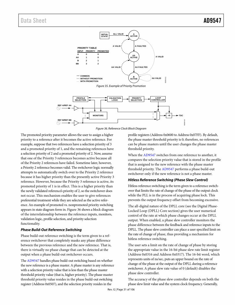
Data Sheet AD9547
Rev. G | Page 31 of 106
AACTIVE
AAACTIVE
BACTIVE
A FAULTED
AA FAULTED
ALL VALIDINITIALSTATE
A VALID
AA VALID
A VALID
AA VALID
INPUT PRIORITY PROMOTEDA 0 0
AA 1 0B 2 1
BB 3 2
PRIORITY TABLE
COMMONWITHOUT PROMOTIONWITH PROMOTION
0830
0-01
1
Figure 35. Example of Priority Promotion
PROFILE
SELECTIONVALIDATION
LOGICPRIORITY
SELECTION
÷RMONITORS
REF A/REF AA
REF B/REF BB
TDC
LOOPCONTROLLER
……
…
0830
0-01
2
Figure 36. Reference Clock Block Diagram
The promoted priority parameter allows the user to assign a higher priority to a reference after it becomes the active reference. For example, suppose that two references have a selection priority of 3 and a promoted priority of 1, and the remaining references have a selection priority of 2 and a promoted priority of 2. Now, assume that one of the Priority 3 references becomes active because all of the Priority 2 references have failed. Sometime later, however, a Priority 2 reference becomes valid. The switchover logic normally attempts to automatically switch over to the Priority 2 reference because it has higher priority than the presently active Priority 3 reference. However, because the Priority 3 reference is active, its promoted priority of 1 is in effect. This is a higher priority than the newly validated reference’s priority of 2, so the switchover does not occur. This mechanism enables the user to give references preferential treatment while they are selected as the active refer-ence. An example of promoted vs. nonpromoted priority switching appears in state diagram form in. Figure 36 shows a block diagram of the interrelationship between the reference inputs, monitors, validation logic, profile selection, and priority selection functionality.
Phase Build-Out Reference Switching
Phase build-out reference switching is the term given to a ref- erence switchover that completely masks any phase difference between the previous reference and the new reference. That is, there is virtually no phase change that can be detected at the output when a phase build-out switchover occurs.
The AD9547 handles phase build-out switching based on whether the new reference is a phase master. A phase master is any reference with a selection priority value that is less than the phase master threshold priority value (that is, higher priority). The phase master threshold priority value resides in the phase build-out switching register (Address 0x0507), and the selection priority resides in the
profile registers (Address 0x0600 to Address 0x07FF). By default, the phase master threshold priority is 0; therefore, no references can be phase masters until the user changes the phase master threshold priority.
When the AD9547 switches from one reference to another, it compares the selection priority value that is stored in the profile that is assigned to the new reference with the phase master threshold priority. The AD9547 performs a phase build-out switchover only if the new reference is not a phase master.
Hitless Reference Switching (Phase Slew Control)
Hitless reference switching is the term given to a reference switch-over that limits the rate of change of the phase of the output clock while the PLL is in the process of acquiring phase lock. This prevents the output frequency offset from becoming excessive.
The all-digital nature of the DPLL core (see the Digital Phase-Locked Loop (DPLL) Core section) gives the user numerical control of the rate at which phase changes occur at the DPLL output. When enabled, a phase slew controller monitors the phase difference between the feedback and reference inputs to the DPLL. The phase slew controller can place a user specified limit on the rate of change of phase, thus providing a mechanism for hitless reference switching.
The user sets a limit on the rate of change of phase by storing the appropriate value in the 16-bit phase slew rate limit register (Address 0x0316 and Address 0x0317). The 16-bit word, which represents units of ns/sec, puts an upper bound on the rate of change of the phase at the output of the DPLL during a reference switchover. A phase slew rate value of 0 (default) disables the phase slew controller.
The accuracy of the phase slew controller depends on both the phase slew limit value and the system clock frequency. Generally,
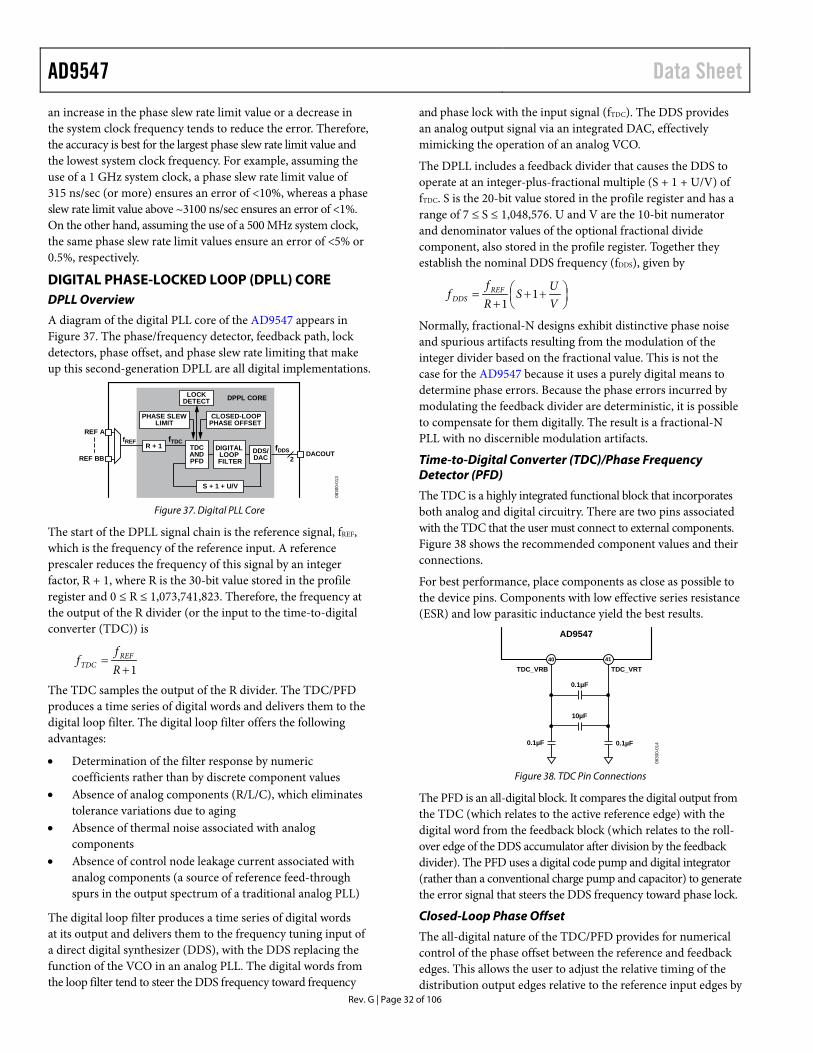
AD9547 Data Sheet an increase in the phase slew rate limit value or a decrease in the system clock frequency tends to reduce the error. Therefore, the accuracy is best for the largest phase slew rate limit value and the lowest system clock frequency. For example, assuming the use of a 1 GHz system clock, a phase slew rate limit value of 315 ns/sec (or more) ensures an error of <10%, whereas a phase slew rate limit value above ~3100 ns/sec ensures an error of <1%. On the other hand, assuming the use of a 500 MHz system clock, the same phase slew rate limit values ensure an error of <5% or 0.5%, respectively.
DIGITAL PHASE-LOCKED LOOP (DPLL) CORE DPLL Overview
A diagram of the digital PLL core of the AD9547 appears in Figure 37. The phase/frequency detector, feedback path, lock detectors, phase offset, and phase slew rate limiting that make up this second-generation DPLL are all digital implementations.
R + 1
REF A
TDCANDPFD
DIGITALLOOPFILTER
DDS/DAC DACOUT
CLOSED-LOOPPHASE OFFSET
PHASE SLEWLIMIT
LOCKDETECT
REF BB
DPPL CORE
2
fREF fTDCfDDS
S + 1 + U/V
0830
0-01
3
Figure 37. Digital PLL Core
The start of the DPLL signal chain is the reference signal, fREF, which is the frequency of the reference input. A reference prescaler reduces the frequency of this signal by an integer factor, R + 1, where R is the 30-bit value stored in the profile register and 0 ≤ R ≤ 1,073,741,823. Therefore, the frequency at the output of the R divider (or the input to the time-to-digital converter (TDC)) is
1+=
Rf
f REFTDC
The TDC samples the output of the R divider. The TDC/PFD produces a time series of digital words and delivers them to the digital loop filter. The digital loop filter offers the following advantages:
• Determination of the filter response by numeric coefficients rather than by discrete component values
• Absence of analog components (R/L/C), which eliminates tolerance variations due to aging
• Absence of thermal noise associated with analog components
• Absence of control node leakage current associated with analog components (a source of reference feed-through spurs in the output spectrum of a traditional analog PLL)
The digital loop filter produces a time series of digital words at its output and delivers them to the frequency tuning input of a direct digital synthesizer (DDS), with the DDS replacing the function of the VCO in an analog PLL. The digital words from the loop filter tend to steer the DDS frequency toward frequency
and phase lock with the input signal (fTDC). The DDS provides an analog output signal via an integrated DAC, effectively mimicking the operation of an analog VCO.
The DPLL includes a feedback divider that causes the DDS to operate at an integer-plus-fractional multiple (S + 1 + U/V) of fTDC. S is the 20-bit value stored in the profile register and has a range of 7 ≤ S ≤ 1,048,576. U and V are the 10-bit numerator and denominator values of the optional fractional divide component, also stored in the profile register. Together they establish the nominal DDS frequency (fDDS), given by
++
+=
VUS
Rf
f REFDDS 1
1
Normally, fractional-N designs exhibit distinctive phase noise and spurious artifacts resulting from the modulation of the integer divider based on the fractional value. This is not the case for the AD9547 because it uses a purely digital means to determine phase errors. Because the phase errors incurred by modulating the feedback divider are deterministic, it is possible to compensate for them digitally. The result is a fractional-N PLL with no discernible modulation artifacts.
Time-to-Digital Converter (TDC)/Phase Frequency Detector (PFD)
The TDC is a highly integrated functional block that incorporates both analog and digital circuitry. There are two pins associated with the TDC that the user must connect to external components. Figure 38 shows the recommended component values and their connections.
For best performance, place components as close as possible to the device pins. Components with low effective series resistance (ESR) and low parasitic inductance yield the best results.
AD9547
10µF
0.1µF
0.1µF0.1µF
TDC_VRTTDC_VRB4140
0830
0-01
4
Figure 38. TDC Pin Connections
The PFD is an all-digital block. It compares the digital output from the TDC (which relates to the active reference edge) with the digital word from the feedback block (which relates to the roll-over edge of the DDS accumulator after division by the feedback divider). The PFD uses a digital code pump and digital integrator (rather than a conventional charge pump and capacitor) to generate the error signal that steers the DDS frequency toward phase lock.
Closed-Loop Phase Offset
The all-digital nature of the TDC/PFD provides for numerical control of the phase offset between the reference and feedback edges. This allows the user to adjust the relative timing of the distribution output edges relative to the reference input edges by
Rev. G | Page 32 of 106
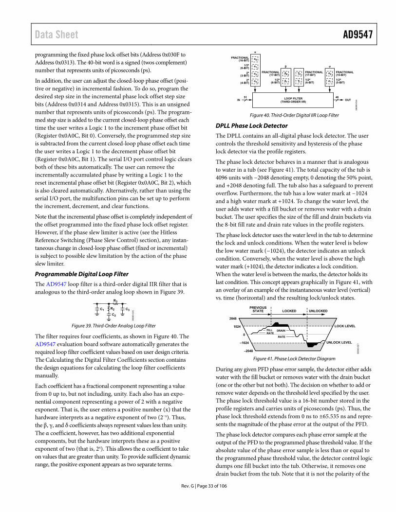
Data Sheet AD9547
Rev. G | Page 33 of 106
programming the fixed phase lock offset bits (Address 0x030F to Address 0x0313). The 40-bit word is a signed (twos complement) number that represents units of picoseconds (ps).
In addition, the user can adjust the closed-loop phase offset (posi-tive or negative) in incremental fashion. To do so, program the desired step size in the incremental phase lock offset step size bits (Address 0x0314 and Address 0x0315). This is an unsigned number that represents units of picoseconds (ps). The program-med step size is added to the current closed-loop phase offset each time the user writes a Logic 1 to the increment phase offset bit (Register 0x0A0C, Bit 0). Conversely, the programmed step size is subtracted from the current closed-loop phase offset each time the user writes a Logic 1 to the decrement phase offset bit (Register 0x0A0C, Bit 1). The serial I/O port control logic clears both of these bits automatically. The user can remove the incrementally accumulated phase by writing a Logic 1 to the reset incremental phase offset bit (Register 0x0A0C, Bit 2), which is also cleared automatically. Alternatively, rather than using the serial I/O port, the multifunction pins can be set up to perform the increment, decrement, and clear functions.
Note that the incremental phase offset is completely independent of the offset programmed into the fixed phase lock offset register. However, if the phase slew limiter is active (see the Hitless Reference Switching (Phase Slew Control) section), any instan-taneous change in closed-loop phase offset (fixed or incremental) is subject to possible slew limitation by the action of the phase slew limiter.
Programmable Digital Loop Filter
The AD9547 loop filter is a third-order digital IIR filter that is analogous to the third-order analog loop shown in Figure 39.
C3
C2
C1 R2
R3
0830
0-01
5
Figure 39. Third-Order Analog Loop Filter
The filter requires four coefficients, as shown in Figure 40. The AD9547 evaluation board software automatically generates the required loop filter coefficient values based on user design criteria. The Calculating the Digital Filter Coefficients section contains the design equations for calculating the loop filter coefficients manually.
Each coefficient has a fractional component representing a value from 0 up to, but not including, unity. Each also has an expo-nential component representing a power of 2 with a negative exponent. That is, the user enters a positive number (x) that the hardware interprets as a negative exponent of two (2−x). Thus, the β, γ, and δ coefficients always represent values less than unity. The α coefficient, however, has two additional exponential components, but the hardware interprets these as a positive exponent of two (that is, 2x). This allows the α coefficient to take on values that are greater than unity. To provide sufficient dynamic range, the positive exponent appears as two separate terms.
LOOP FILTER(THIRD-ORDER IIR)
IN OUT
FRACTIONAL(16-BIT)
1/2x
(6-BIT)
α0
α
β0
β1
0
1
β
σ0
σ1
σα1
α2
α3
2x
(3-BIT)
2x
(4-BIT)
FRACTIONAL(17-BIT)
1/2x
(6-BIT)
FRACTIONAL(17-BIT)
1/2x
(6-BIT)
FRACTIONAL(15-BIT)
1/2x
(5-BIT)
4851
0830
0-01
6
Figure 40. Third-Order Digital IIR Loop Filter
DPLL Phase Lock Detector
The DPLL contains an all-digital phase lock detector. The user controls the threshold sensitivity and hysteresis of the phase lock detector via the profile registers.
The phase lock detector behaves in a manner that is analogous to water in a tub (see Figure 41). The total capacity of the tub is 4096 units with −2048 denoting empty, 0 denoting the 50% point, and +2048 denoting full. The tub also has a safeguard to prevent overflow. Furthermore, the tub has a low water mark at −1024 and a high water mark at +1024. To change the water level, the user adds water with a fill bucket or removes water with a drain bucket. The user specifies the size of the fill and drain buckets via the 8-bit fill rate and drain rate values in the profile registers.
The phase lock detector uses the water level in the tub to determine the lock and unlock conditions. When the water level is below the low water mark (−1024), the detector indicates an unlock condition. Conversely, when the water level is above the high water mark (+1024), the detector indicates a lock condition. When the water level is between the marks, the detector holds its last condition. This concept appears graphically in Figure 41, with an overlay of an example of the instantaneous water level (vertical) vs. time (horizontal) and the resulting lock/unlock states.
0
2048
–2048
1024
–1024
LOCK LEVEL
UNLOCK LEVEL
LOCKED UNLOCKEDPREVIOUS
STATE
FILLRATE
DRAIN
RATE
0830
0-01
7
Figure 41. Phase Lock Detector Diagram
During any given PFD phase error sample, the detector either adds water with the fill bucket or removes water with the drain bucket (one or the other but not both). The decision on whether to add or remove water depends on the threshold level specified by the user. The phase lock threshold value is a 16-bit number stored in the profile registers and carries units of picoseconds (ps). Thus, the phase lock threshold extends from 0 ns to ±65.535 ns and repre-sents the magnitude of the phase error at the output of the PFD.
The phase lock detector compares each phase error sample at the output of the PFD to the programmed phase threshold value. If the absolute value of the phase error sample is less than or equal to the programmed phase threshold value, the detector control logic dumps one fill bucket into the tub. Otherwise, it removes one drain bucket from the tub. Note that it is not the polarity of the

AD9547 Data Sheet phase error sample but, rather, its magnitude relative to the phase threshold value that determines whether to fill or drain. If more filling is taking place than draining, the water level in the tub eventually rises above the high water mark (+1024), which causes the phase lock detector to indicate lock. If more draining is taking place than filling, the water level in the tub eventually falls below the low water mark (−1024), which causes the phase lock detector to indicate unlock. The ability to specify the threshold level, fill rate, and drain rate enables the user to tailor the operation of the phase lock detector to the statistics of the timing jitter associated with the input reference signal.
Note that when the AD9547 enters the free-run or holdover mode, the DPLL phase lock detector indicates unlocked. Also, when the AD9547 performs a reference switchover, the state of the lock detector prior to the switch is preserved during the transition period.
DPLL Frequency Lock Detector
The operation of the frequency lock detector is identical to that of the phase lock detector. The only difference is that the fill or drain decision is based on the period deviation between the reference and feedback signals of the DPLL instead of the phase error at the output of the PFD.
The frequency lock detector uses a 24-bit frequency threshold register specified in units of picoseconds (ps). Thus, the fre-quency threshold value extends from 0 µs to ±16.777215 µs.
It represents the magnitude of the difference in period between the reference and feedback signals at the input to the DPLL. For example, if the reference signal is 1.25 MHz and the feedback signal is 1.38 MHz, the period difference is approximately 75.36 ns (|1/1,250,000 − 1/1,380,000| ≈ 75.36 ns).
DIRECT DIGITAL SYNTHESIZER (DDS) DDS Overview
One of the primary building blocks of the digital PLL is a direct digital synthesizer (DDS). The DDS behaves like a sinusoidal signal generator. The frequency of the sinusoid generated by the DDS is determined by a frequency tuning word (FTW), which is a digital (that is, numeric) value. Unlike an analog sinusoidal generator, a DDS uses digital building blocks and operates as a sampled system. Thus, it requires a sampling clock (fS) that serves as the fundamental timing source of the DDS. The accumulator behaves as a modulo-248 counter with a programmable step size (FTW). A block diagram of the DDS appears in Figure 42.
The input to the DDS is the 48-bit FTW. The FTW serves as a step size value. On each cycle of fS, the accumulator adds the value of the FTW to the running total at its output. For example, given that FTW = 5, the accumulator counts by fives, incre-menting on each fS cycle. Over time, the accumulator reaches the upper end of its capacity (248 in this case), at which point, it rolls over but retains the excess. The average rate at which the accumulator rolls over establishes the frequency of the output sinusoid. The average rollover rate of the accumulator establishes the output frequency (fDDS) of the DDS and is given by
SDDS fFTW
f
=
482
Solving this equation for FTW yields
=
S
DDS
ff
FTW 482round
For example, given that fS = 1 GHz and fDDS = 155.52 MHz, then FTW = 43,774,988,378,041 (0x27D028A1DFB9).
Note that the minimum DAC output frequency is 62.5 MHz; therefore, normal operation requires an FTW that yields an output frequency in excess of this lower bound.
DAC(14-BIT)
PHASEOFFSET
QD
fS
FREQUENCYTUNING WORD
(FTW)
DAC+
DAC–
1419
48
19 ANGLE TOAMPLITUDE
CONVERSION
4848
48-BIT ACCUMULATOR
16
0830
0-01
8
Figure 42. DDS Block Diagram
Rev. G | Page 34 of 106

Data Sheet AD9547
Rev. G | Page 35 of 106
DDS Phase Offset
The relative phase of the sinusoid generated by the DDS is numer-ically controlled by adding a phase offset word to the output of the DDS accumulator. This is accomplished via the open loop phase offset register (Address 0x030D to Address 0x030E), which is a programmable 16-bit value (Δphase). The resulting phase offset, ΔΦ (radians), is given by
1622
phaseΦ
Phase offset and relative time offset are directly related. The time offset is (Δphase/216)/fDDS (seconds), where fDDS is the output frequency of the DDS (Hz).
DAC Output
The output of the digital core of the DDS is a time series of numbers representing a sinusoidal waveform. The DAC translates the numeric values to an analog signal. The DAC output signal appears at two pins that constitute a balanced current source architecture (see Figure 43).
CURRENTSWITCHARRAY
SWITCHCONTROL
IFS
ISCALE
AVDD3
DACOUTP DACOUTN
CURRENTMIRROR
GND
16
GND
13 14
CODE
CODE
50Ω50Ω14
10
IFS 1–214 – 1
CODEIFS
214 – 1
0830
0-01
9
Figure 43. DAC Output Pins
The value of IFS is programmable via the 10-bit DAC full-scale current word in the DAC current register (Address 0x0213 and Address 0x0214). The value of the 10-bit word (ISCALE) sets IFS according to the following formula:
IFS = 120 μA × (72 +
163 × ISCALE)
TUNING WORD PROCESSING The frequency tuning words that dictate the output frequency of the DDS come from one of three sources (see Figure 44).
The free-running frequency tuning word register The output of the digital loop filter The output of the tuning word history processor
TUNING WORDHISTORY
PROCESSOR
TUNING WORDHISTORY
FREE-RUNTUNING WORD
TUNING WORDUPDATE
FROM DIGITALLOOP FILTER
TO DDSTUNINGWORD
ROUTINGCONTROL
TUNINGWORDCLAMP
LOWERTUNINGWORD
UPPERTUNINGWORD
0830
0-07
0
Figure 44. Tuning Word Processing
When the DPLL is in free-run mode, the DDS tuning word is the value stored in the free-running frequency tuning word register (Address 0x0300 to Address 0x0305). When the DPLL is operating normally (closed loop), the DDS tuning word comes from the output of the digital loop filter, which changes dynami-cally to maintain phase lock with the input reference signal (assuming that the device has not performed an automatic switch to holdover mode). When the DPLL is in holdover mode, the DDS tuning word depends on a historical record of past tuning words during the time that the DPLL operated in closed-loop mode.
However, regardless of the operating mode, the DDS output frequency is ultimately subject to the boundary conditions imposed by the frequency clamp logic as explained in the Frequency Clamp section.
Frequency Clamp
The user controls the frequency clamp boundaries via the pull-in range limit registers (Address 0x0307 to Address 0x030C). These registers allow the user to fix the DDS output frequency between an upper and lower bound with a granularity of 24 bits. Note that these upper and lower bounds apply regardless of the frequency tuning word that appears at the input to the DDS. The register value relates to the absolute upper or lower frequency bound (fCLAMP) as
fCLAMP = fS × (N/224)
where N is the value stored in the upper- or lower-limit register, and fS is the system sample rate.
Even though the frequency clamp limits put a bound on the DDS output frequency, the DPLL is still free to steer the DDS frequency within the clamp limits. The default register values set the clamp range from 0 Hz (dc) to fS, effectively eliminating the frequency clamp functionality until the user alters the register values.
Frequency Tuning Word History
The AD9547 has the ability to track the history of the tuning word samples generated by the DPLL digital loop filter output. It does so by periodically computing the average tuning word value over a user specified interval. The user programs the interval via the 24-bit history accumulation timer register (Address 0x0318 to Address 0x031A). This 24-bit value repre-sents a time interval (TAVG) in units of milliseconds (ms) that extends from 1 ms to a maximum of 4:39:37.215 (hr:min:sec).
Note that history accumulation timer = 0 should not be pro-grammed because it may cause improper device operation.
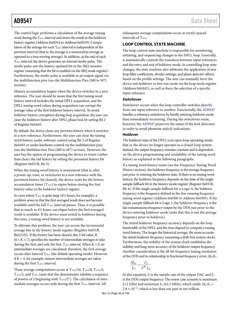
AD9547 Data Sheet The control logic performs a calculation of the average tuning word during the TAVG interval and stores the result in the holdover history register (Address 0x0D14 to Address 0x0D19). Compu-tation of the average for each TAVG interval is independent of the previous interval (that is, the average is a memoryless average as opposed to a true moving average). In addition, at the end of each TAVG interval, the device generates an internal strobe pulse. The strobe pulse sets the history updated bit in the IRQ monitor register (assuming that the bit is enabled via the IRQ mask register). Furthermore, the strobe pulse is available as an output signal via the multifunction pins (see the Multifunction Pins (M0 to M7) section).
History accumulation begins when the device switches to a new reference. The user should be aware that the first tuning word history interval includes the initial DPLL acquisition, and the DPLL tuning word values during acquisition can corrupt the average value of the first holdover history interval. To avoid holdover history corruption during loop acquisition, the user can clear the holdover history after DPLL phase lock by setting Bit 2 of Register 0x0A03.
By default, the device clears any previous history when it switches to a new reference. Furthermore, the user can clear the tuning word history under software control using Bit 2 of Register 0x0A03 or under hardware control via the multifunction pins (see the Multifunction Pins (M0 to M7) section). However, the user has the option of programming the device to retain (rather than clear) the old history by setting the persistent history bit (Register 0x031B, Bit 3).
When the tuning word history is nonexistent (that is, after a power-up, reset, or switchover to a new reference with the persistent history bit cleared), the device waits for the history accumulation timer (TAVG) to expire before storing the first history value in the holdover history register.
In cases where TAVG is quite large (4½ hours, for example), a problem arises in that the first averaged result does not become available until the full TAVG interval passes. Thus, it is possible that as much as 4½ hours can elapse before the first averaged result is available. If the device must switch to holdover during this time, a tuning word history is not available.
To alleviate this problem, the user can access the incremental average bits in the history mode register (Register 0x031B, Bits[2:0]). If the history has been cleared, this 3-bit value, K (0 ≤ K ≤ 7), specifies the number of intermediate averages to take during the first, and only the first, TAVG interval. When K = 0, no intermediate averages are calculated; therefore, the first average occurs after Interval TAVG (the default operating mode). However, if K = 4, for example, sixteen intermediate averages are taken during the first TAVG interval.
These average computations occur at TAVG/16, TAVG/8, TAVG/4, TAVG/2, and TAVG (note that the denominator exhibits a sequence of powers of 2 beginning with TAVG/2K). The calculation of inter-mediate averages occurs only during the first TAVG interval. All
subsequent average computations occur at evenly spaced intervals of TAVG.
LOOP CONTROL STATE MACHINE The loop control state machine is responsible for monitoring, initiating, and sequencing changes to the DPLL loop. Generally, it automatically controls the transition between input references and the entry and exit of holdover mode. In controlling loop state changes, the state machine also arbitrates the application of new loop filter coefficients, divider settings, and phase detector offsets based on the profile settings. The user can manually force the device into holdover or free-run mode via the loop mode register (Address 0x0A01), as well as force the selection of a specific input reference.
Switchover
Switchover occurs when the loop controller switches directly from one input reference to another. Functionally, the AD9547 handles a reference switchover by briefly entering holdover mode then immediately recovering. During the switchover event, however, the AD9547 preserves the status of the lock detectors in order to avoid phantom unlock indications.
Holdover
The holdover state of the DPLL is an open-loop operating mode; that is, the device no longer operates as a closed-loop system. Instead, the output frequency remains constant and is dependent on the device programming and availability of the tuning word history as explained in the following paragraphs. If a tuning word history exists (see the Frequency Tuning Word History section), the holdover frequency is the average frequency just prior to entering the holdover state. If there is no tuning word history, the holdover frequency depends on the state of the single sample fallback bit in the history mode register (Register 0x031B, Bit 4). If the single sample fallback bit is Logic 0, the holdover frequency is the frequency defined in the free-running frequency tuning word register (Address 0x0300 to Address 0x0305). If the single sample fallback bit is Logic 1, the holdover frequency is the last instantaneous frequency output by the DDS just prior to the device entering holdover mode (note that this is not the average frequency prior to holdover). The initial holdover frequency accuracy depends on the loop bandwidth of the DPLL and the time elapsed to compute a tuning word history. The longer the historical average, the more accurate the initial holdover frequency (assuming a drift-free system clock). Furthermore, the stability of the system clock establishes the stability and long-term accuracy of the holdover output frequency. Another consideration is the 48-bit frequency tuning resolution of the DDS and its relationship to fractional frequency error, ∆fO/fO.
O
S
O
O
ff
ff
492=
∆
In this equation, fS is the sample rate of the output DAC and fO is the DDS output frequency. The worst-case scenario is maximum fS (1 GHz) and minimum fO (62.5 MHz), which yields ∆fO/fO = 2.8 × 10⁻¹⁴, which is less than one part in ten trillion.
Rev. G | Page 36 of 106

Data Sheet AD9547 Recovery from Holdover
When in holdover, if a valid reference becomes available, the device exits holdover operation. The loop state machine restores the DPLL to closed-loop operation, locks to the selected reference, and sequences the recovery of all the loop parameters based on the profile settings for the active reference.
Note that if the user holdover bit (Register 0x0A01, Bit 6) is set, the device does not automatically exit holdover when a valid reference is available. However, automatic recovery can occur after clearing the user holdover bit.
SYSTEM CLOCK INPUTS Functional Description
The system clock circuit provides a low jitter, stable, high fre-quency clock for use by the rest of the chip. The user has the option of directly driving the SYSCLKx inputs with a high frequency clock source at the desired system clock rate. Alternatively, the SYSCLKx input can be configured to operate in conjunction with the internal SYSCLK PLL. The SYSCLK PLL can synthesize the system clock by means of a crystal resonator connected across the SYSCLKx input pins or by means of direct application of a low frequency clock source.
The SYSCLKx inputs are internally biased to a dc level of ~1 V. Take care to ensure that any external connections do not disturb the dc bias because such a disturbance can significantly degrade performance. Generally, the SYSCLKx inputs should be ac-coupled to the signal source (except when using a crystal resonator).
Low Loop Bandwidth Applications Using a TCXO/OCXO
For many applications, the use of a crystal oscillator is a cost-effective and simple choice. The stability is good enough to support loop bandwidths down to 50 Hz, and the holdover performance is good enough for all except the most demanding applications.
In cases where Stratum 2 or Stratum 3 holdover performance is needed, or in cases where the loop bandwidth must be <50 Hz, either a TCXO or OCXO must be used. If the loop bandwidths are lower than 10 millihertz, an OCXO must be used. Choose a TCXO/OCXO with a high output frequency and CMOS output to achieve the best performance. AN-1079 Application Note,
Determining the Maximum Tolerable Frequency Drift Rate of the AD9548 System Clock in Low Loop Bandwidth Applications discusses system clock performance considerations for low loop bandwidth applications.
When interfacing the TCXO/OCXO, a voltage divider on the output should be used to reduce the voltage swing to 1 V p-p, and that signal should be ac-coupled to the SYSCLKP pin. The SYSCLKN pin can be bypassed to ground with a 0.01 µF capacitor.
Choosing the System Clock Oscillator Frequency
The best performance of the AD9548 is achieved when the system clock is not an integer multiple of the DDS output frequency.
As an example, using a 19.44 MHz oscillator for the system clock in a 156.25 MHz Ethernet application yields better performance than a 25 MHz oscillator.
Another good system clock choice for many communications applications is a 49.152 MHz crystal used in IEEE 1394 (FireWire) because nearly all output frequencies are not integer related to this frequency and the crystal is readily available.
System Clock Details
A block diagram of the system clock appears in Figure 45. The signal at the SYSCLKx input pins becomes the internally buffered DAC sampling clock (fS) via one of three paths.
• High frequency direct (HF) • Low frequency synthesized (LF) • Crystal resonator synthesized (XTAL)
Note that both the LF and XTAL paths require the use of the SYSCLK PLL (see the SYSCLK PLL Multiplier section).
The main purpose of the HF path is to allow the direct use of a high frequency (500 MHz to 1 GHz) external clock source for clocking the AD9547. This path is optimized for high frequency and low noise floor. Note that the HF input also provides a path to SYSCLK PLL (see the SYSCLK PLL Multiplier section), which includes an input divider (M) programmable for divide-by −1, −2, −4, or −8. The purpose of the divider is to limit the frequency at the input to the PLL to less than 150 MHz, which is the maxi-mum PFD rate.
Rev. G | Page 37 of 106
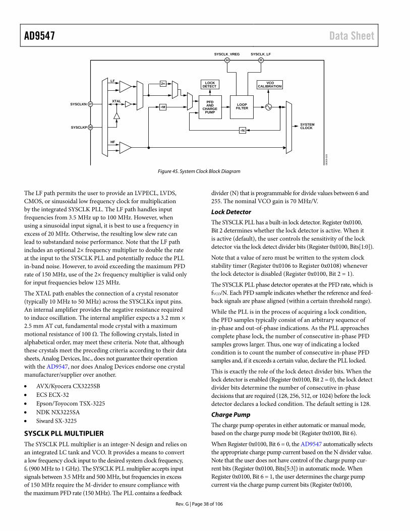
AD9547 Data Sheet
2×
÷N
VCOCALIBRATION
LOCKDETECT
SYSTEMCLOCK
÷M LOOPFILTER
SYSCLKN
SYSCLKP
SYSCLK_VREG SYSCLK_LF
HF
XTAL
LF
34
37
38
35
PFDAND
CHARGEPUMP
0830
0-02
0
Figure 45. System Clock Block Diagram
The LF path permits the user to provide an LVPECL, LVDS, CMOS, or sinusoidal low frequency clock for multiplication by the integrated SYSCLK PLL. The LF path handles input frequencies from 3.5 MHz up to 100 MHz. However, when using a sinusoidal input signal, it is best to use a frequency in excess of 20 MHz. Otherwise, the resulting low slew rate can lead to substandard noise performance. Note that the LF path includes an optional 2× frequency multiplier to double the rate at the input to the SYSCLK PLL and potentially reduce the PLL in-band noise. However, to avoid exceeding the maximum PFD rate of 150 MHz, use of the 2× frequency multiplier is valid only for input frequencies below 125 MHz.
The XTAL path enables the connection of a crystal resonator (typically 10 MHz to 50 MHz) across the SYSCLKx input pins. An internal amplifier provides the negative resistance required to induce oscillation. The internal amplifier expects a 3.2 mm × 2.5 mm AT cut, fundamental mode crystal with a maximum motional resistance of 100 Ω. The following crystals, listed in alphabetical order, may meet these criteria. Note that, although these crystals meet the preceding criteria according to their data sheets, Analog Devices, Inc., does not guarantee their operation with the AD9547, nor does Analog Devices endorse one crystal manufacturer/supplier over another.
• AVX/Kyocera CX3225SB • ECS ECX-32 • Epson/Toyocom TSX-3225 • NDK NX3225SA • Siward SX-3225
SYSCLK PLL MULTIPLIER The SYSCLK PLL multiplier is an integer-N design and relies on an integrated LC tank and VCO. It provides a means to convert a low frequency clock input to the desired system clock frequency, fS (900 MHz to 1 GHz). The SYSCLK PLL multiplier accepts input signals between 3.5 MHz and 500 MHz, but frequencies in excess of 150 MHz require the M-divider to ensure compliance with the maximum PFD rate (150 MHz). The PLL contains a feedback
divider (N) that is programmable for divide values between 6 and 255. The nominal VCO gain is 70 MHz/V.
Lock Detector
The SYSCLK PLL has a built-in lock detector. Register 0x0100, Bit 2 determines whether the lock detector is active. When it is active (default), the user controls the sensitivity of the lock detector via the lock detect divider bits (Register 0x0100, Bits[1:0]).
Note that a value of zero must be written to the system clock stability timer (Register 0x0106 to Register 0x0108) whenever the lock detector is disabled (Register 0x0100, Bit 2 = 1).
The SYSCLK PLL phase detector operates at the PFD rate, which is fVCO/N. Each PFD sample indicates whether the reference and feed-back signals are phase aligned (within a certain threshold range).
While the PLL is in the process of acquiring a lock condition, the PFD samples typically consist of an arbitrary sequence of in-phase and out-of-phase indications. As the PLL approaches complete phase lock, the number of consecutive in-phase PFD samples grows larger. Thus, one way of indicating a locked condition is to count the number of consecutive in-phase PFD samples and, if it exceeds a certain value, declare the PLL locked.
This is exactly the role of the lock detect divider bits. When the lock detector is enabled (Register 0x0100, Bit 2 = 0), the lock detect divider bits determine the number of consecutive in-phase decisions that are required (128, 256, 512, or 1024) before the lock detector declares a locked condition. The default setting is 128.
Charge Pump
The charge pump operates in either automatic or manual mode, based on the charge pump mode bit (Register 0x0100, Bit 6).
When Register 0x0100, Bit 6 = 0, the AD9547 automatically selects the appropriate charge pump current based on the N divider value. Note that the user does not have control of the charge pump cur-rent bits (Register 0x0100, Bits[5:3]) in automatic mode. When Register 0x0100, Bit 6 = 1, the user determines the charge pump current via the charge pump current bits (Register 0x0100,
Rev. G | Page 38 of 106

Data Sheet AD9547 Bits[5:3]). The charge pump current varies from 125 µA to 1 mA in 125 µA steps. The default setting is 500 µA.
SYSCLK PLL Loop Filter
The AD9547 has an internal second-order loop filter that estab-lishes the loop dynamics for input signals between 12.5 MHz and 100 MHz. By default, the device uses the internal loop filter. However, an external loop filter option is available by setting the external loop filter enable bit (Register 0x0100, Bit 7). This bit bypasses the internal loop filter and allows the device to use an externally connected second-order loop filter, as shown in Figure 46.
SYSCLK_VREG
R1
AD9547
SYSCLK_LF
C1
C2
34 35
0830
0-02
1
Figure 46. External Loop Filter Schematic
To determine the external loop filter components, the user decides on the desired open loop bandwidth (fOL) and phase margin (Φ). These parameters allow calculation of the loop filter components, as follows:
R1 = ( )
φ
+π
sin11
VCOCP
OL
KINf
C1 = 2)(2)tan(
OL
VCOCP
fNKI
π
φ
C2 =
φ
φ−
π )cos()sin(1
)2( 2OL
VCOCP
fNKI
where: KVCO = 7 × 10⁷ V/ns (typical). ICP is the programmed charge pump current (amperes). N is the programmed feedback divider value. fOL is the desired open-loop bandwidth (Hz). Φ is the desired phase margin (radians).
For example, assuming that N = 40, ICP = 0.5 mA, fOL = 400 kHz, and Φ = 50°, then the loop filter calculations yield R1 = 3.31 kΩ, C1 = 330 pF, and C2 = 50.4 pF.
System Clock Period
Many of the user programmable parameters of the AD9547 have absolute time units. To make this possible, the AD9547 requires a priori knowledge of the period of the system clock. To accom-modate this requirement, the user programs the 21-bit nominal system clock period in the nominal SYSCLK period register (Address 0x0103 to Address 0x0105). The contents of this register reflect the actual period of the system clock in units of femto-seconds (fs). The user must program this register properly to ensure proper operation of the device because many of its subsystems rely on this value.
System Clock Stability Timer
The system clock stability timer, located in Register 0x0106 to Register 0x0108, is a 20-bit value programmed in units of milli-seconds (ms). If the programmed timer value is 0, the timer immediately indicates that it has timed out. If the programmed timer value is nonzero and the SYSCLK PLL is enabled, the timer starts timing when the SYSCLK PLL lock detector indicates lock and times out after the prescribed period. However, when the user disables the SYSCLK PLL, the timer ignores the SYSCLK PLL lock detector and starts timing the instant that the SYSCLK PLL is disabled. The user can monitor the status of the stability timer at Register 0x0D01, Bit 4, via the multifunction pins or via the IRQ pin.
Note that the system clock stability timer must be programmed before the SYSCLK PLL is either activated or disabled.
SYSCLK PLL Calibration
When using the SYSCLK PLL, it is necessary to calibrate the LC-VCO to ensure that the PLL can remain locked to the system clock input signal. Assuming the presence of either an external SYSCLK input signal or a crystal resonator, the calibration process executes after the user sets and then clears the calibrate system clock bit in the cal/sync register (Register 0x0A02, Bit 0). During the calibration process, the device calibrates the VCO amplitude and frequency. The status of the system clock calibration process is user accessible via the system clock status register (Register 0x0D01, Bit 1). It is also available via the IRQ monitor register (Bit 1 of Register 0x0D02), provided that the status bit is enabled via the IRQ mask register (Register 0x0209 and Register 0x0210).
When the calibration sequence is complete, the SYSCLK PLL eventually attains a lock condition, at which point the system clock stability timer begins its countdown sequence. Expiration of the timer indicates that the SYSCLK PLL is stable, which is reflected in the system clock status register (Register 0x0D01, Bit 4).
Note that the monitors/detectors associated with the input references (REF A/REF AA and REF B/REF BB) are internally disabled until the SYSCLK PLL indicates that it is stable.
CLOCK DISTRIBUTION The clock distribution block of the AD9547 provides an integrated solution for generating multiple clock outputs based on frequency dividing the DPLL output. The distribution output consists of two channels (OUT0 and OUT1). Each channel has a dedicated divider and output driver section, as shown in Figure 47.
Rev. G | Page 39 of 106

AD9547 Data Sheet
Rev. G | Page 40 of 106
Q0
SYNCCONTROL
ENABLEn/MODEn
SYNC SOURCE
CLKINP
OUT1POUT1N
OUT1
OUT0
CLKINN
OUT_RSET
OUT0P
OUT0N
RES
ET
ENA
BLE
4 4 4
0830
0-02
2
Figure 47. Clock Distribution
Clock Input (CLKINx)
The clock input handles input signals from a variety of logic families (assuming proper terminations and sufficient voltage swing). It also handles sine wave input signals such as those delivered by the DAC reconstruction filter. Its default operating frequency range is 62.5 MHz to 500 MHz.
Super-Nyquist Operation
Typically, the maximum usable frequency at the DAC output is about 45% of the system clock frequency. However, because it is a sampled DAC, its output spectrum contains Nyquist images. Of particular interest are the images appearing in the first Nyquist zone (50% to 100% of the system clock frequency). Super-Nyquist operation takes advantage of these higher frequencies, but this implies that the CLKINx input operates in excess of 500 MHz, which is outside its default operating limits.
The CLKINx receiver actually consists of two separate receivers: the default receiver and an optional high frequency receiver, which handles input signals up to 800 MHz. To select the high frequency receiver, write a Logic 1 to Register 0x0400, Bit4.
Super-Nyquist operation requires a band-pass filter at the DAC output instead of the usual low-pass reconstruction filter. Super-Nyquist operation is viable as long as the image frequency does not exceed the 800 MHz input range of the receiver. Furthermore, to provide acceptable jitter performance, which is a consideration for image signals with low amplitude, the signal at the CLKINx inputs must meet the minimum slew rate requirements.
Clock Dividers
The output clock distribution dividers are referred to as Q0 and Q1, corresponding to the OUT0 and OUT1 output channels, respec-tively. Each divider is programmable with 30 bits of division depth. The actual divide ratio is one more than the programmed register value; therefore, a register value of 3, for example, results in a divide ratio of 4. Thus, each divider offers a range of divide ratios from 1 to 230 (1 to 1,073,741,824).
With an even divide ratio, the output signal always exhibits a 50% duty cycle. When the clock divider is bypassed (a divide
ratio of 1), the output duty cycle is the same as the input duty cycle. Odd output divide ratios (excluding 1) exhibit automatic duty cycle correction given by
NXNCycleDutyOutput
212
where: N (which must be an odd number) is the divide ratio. X is the normalized fraction of the high portion of the input period (that is, 0 < X < 1).
For example, if N = 5 and the input duty cycle is 20% (X = 0.2), then the output duty cycle is 44%. Note that, when the user programs an output as noninverting, then the device adjusts the falling edge timing to accomplish the duty cycle correction. Conversely, the device adjusts the rising edge timing for an inverted output.
Output Power-Down
Each output channel offers independent control of power-down functionality via the distribution settings register (Address 0x0400). Each output channel has a dedicated power-down bit for powering down the output driver. However, if both channels are powered down, the entire distribution output enters a deep sleep mode.
Even though each channel has a channel power-down control signal, it may sometimes be desirable to power down an output driver while maintaining the divider’s synchronization with the other channel dividers. This is accomplished by either of the following methods:
In CMOS mode, use the divider output enable control bit to stall an output. This provides power savings while main-taining dc drive at the output.
In LVDS/LVPECL mode, place the output in tristate mode (this works in CMOS mode as well).
Output Enable
Each output channel offers independent control of enable/ disable functionality using the distribution enable register (Address 0x0401). The distribution outputs use synchronization logic to control enable/disable activity to avoid the production of runt pulses and to ensure that outputs with the same divide ratios become active/inactive in unison.
Output Mode
The user has independent control of the operating mode of each of the two output channels via the distribution channel modes register (Address 0x0404 and Address 0x0405). The operating mode control includes
Logic family and pin functionality Output drive strength Output polarity
The three LSBs of both distribution channel mode registers com-prise the mode bits. The mode value selects the desired logic family and pin functionality of an output channel, as listed in Table 24.

Data Sheet AD9547 Table 24. Output Channel Logic Family and Pin Functionality Mode Bits [2:0] Logic Family and Pin Functionality 000 CMOS (both pins) 001 CMOS (positive pin), tristate (negative pin) 010 Tristate (positive pin), CMOS (negative pin) 011 Tristate (both pins) 100 LVDS 101 LVPECL 110 Unused 111 Unused
Regardless of the selected logic family, each is capable of dc operation. However, the upper frequency is limited by the load conditions, drive strength, and impedance matching inherent in each logic family. Practical limitations set the maximum CMOS frequency to approximately 250 MHz, whereas LVPECL and LVDS are capable of 725 MHz.
In addition to the three mode bits, both distribution channel mode registers include the following control bits:
• Polarity invert • CMOS phase invert • Drive strength
The polarity invert bit enables the user to choose between normal polarity and inverted polarity. Normal polarity is the default state. Inverted polarity reverses the representation of Logic 0 and Logic 1 regardless of the logic family.
The CMOS phase invert bit applies only when the mode bits select the CMOS logic family. In CMOS mode, both output pins of the channel have a dedicated CMOS driver. By default, both drivers deliver identical signals. However, setting the CMOS phase invert bit causes the signal on an OUTxN pin to be the opposite of the signal appearing on the OUTxP pin.
The drive strength bit allows the user to control whether the output uses weak (0) or strong (1) drive capability (applies to CMOS and LVDS but not LVPECL). For the CMOS family, the strong setting implies normal CMOS drive capability, whereas the weak setting implies low capacitive loading and allows for reduced EMI. For the LVDS family, the weak setting provides 3.5 mA drive current for standard LVDS operation, whereas the strong setting provides 7 mA for double terminated or double voltage LVDS operation. Note that 3.5 mA and 7 mA are the nominal drive current values when using the internal current setting resistor.
Output Current Control with an External Resistor
By default, the output drivers have an internal current setting resistor (3.12 kΩ nominal) that establishes the nominal drive current for the LVDS and LVPECL operating modes. Instead of using the internal resistor, the user can elect to set the external distribution resistor bit (Register 0x0400, Bit 5) and connect an external resistor to the OUT_RSET pin. Note that this feature supports an external resistor value of 3.12 kΩ only, allowing for tighter control of the output current than is possible by using
the internal current setting resistor. However, if the user elects to use a nonstandard external resistance, the following equations provide the output drive current as a function of the external resistance (R):
RI
0LVDS8325.10
=
RI
1LVDS665.21
=
RI LVPECL
76.24=
The numeric subscript associated with the LVDS output cur-rent corresponds to the logic state of the drive strength bit in the distribution channel modes registers (Address 0x0404, Bit 3 and Address 0x0405, Bit 3). For R = 3.12 kΩ, the equations yield ILVDS0 = 3.5 mA, ILVDS1 = 7.0 mA, and ILVPECL = 8.0 mA. Note that the device maintains a constant 1.238 V (nominal) across the external resistor.
Clock Distribution Synchronization
A block diagram of the distribution synchronization functionality appears in Figure 48. The synchronization sequence begins with the primary synchronization signal, which ultimately results in delivery of a synchronization strobe to the clock distribution logic.
As indicated, the primary synchronization signal originates from the following four possible sources:
• Direct synchronization source via the sync distribution bit (Register 0x0A02, Bit 1)
• Automatic synchronization source based on frequency or phase lock detection, as controlled via the automatic synchro-nization register (Address 0x0403)
• Multifunction pin synchronization source via one of the multifunction pins (M0 to M7)
• EEPROM synchronization source via the EEPROM
All four sources of the primary synchronization signal are logic OR’d, so any one of them can synchronize the clock distribution output at any time. When using the multifunction pins, the syn-chronization event is the falling edge of the selected signal. When using the sync distribution bit, the user first sets then clears the bit. The synchronization event is the clearing operation; that is, the Logic 1 to Logic 0 transition of the bit.
The primary synchronization signal can synchronize the distribution output directly, or it can enable a secondary synchronization signal. This functionality depends on the two sync source bits in the distribution synchronization register (Register 0x0402, Bits[5:4]).
When sync source = 00 (direct), the falling edge of the primary synchronization signal directly synchronizes the distribution output.
When sync source = 01, the rising edge of the primary synchroni-zation signal triggers the circuitry that detects a rising edge of the
Rev. G | Page 41 of 106
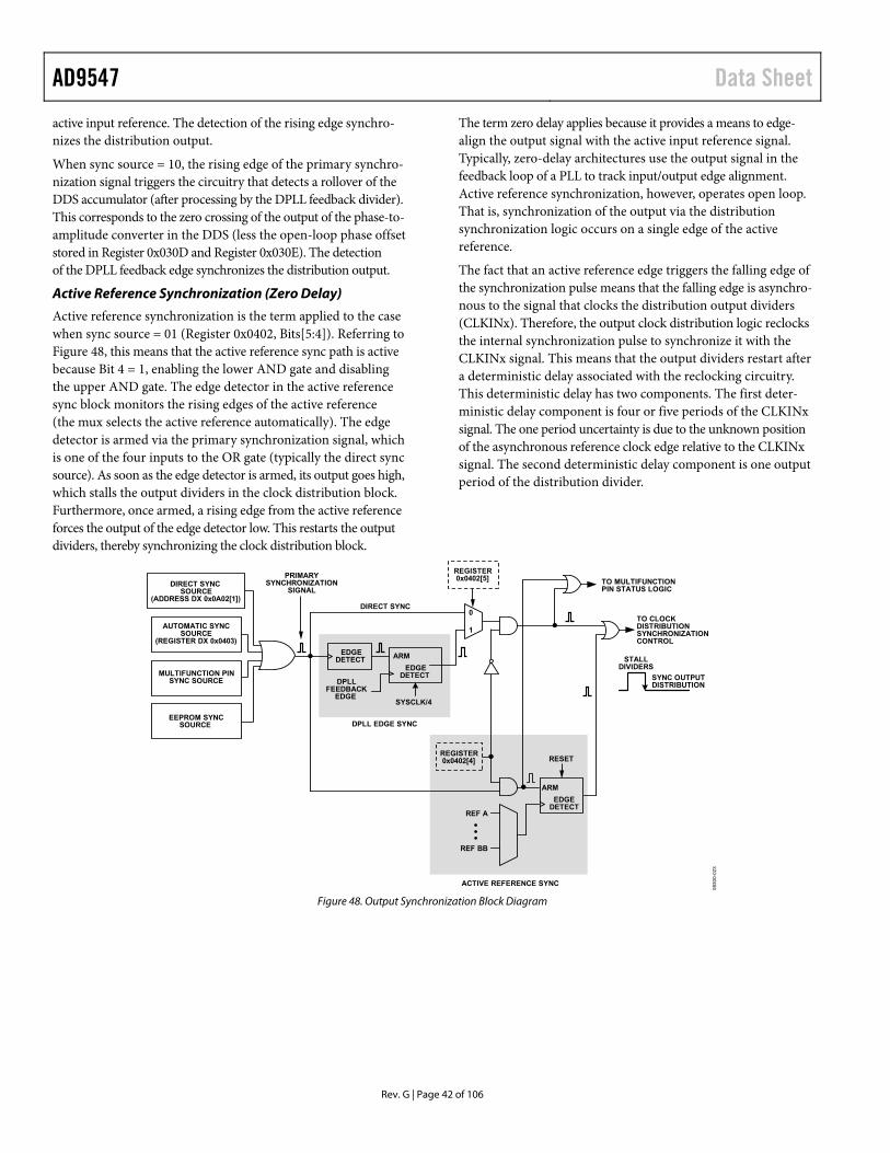
AD9547 Data Sheet
Rev. G | Page 42 of 106
active input reference. The detection of the rising edge synchro-nizes the distribution output.
When sync source = 10, the rising edge of the primary synchro-nization signal triggers the circuitry that detects a rollover of the DDS accumulator (after processing by the DPLL feedback divider). This corresponds to the zero crossing of the output of the phase-to-amplitude converter in the DDS (less the open-loop phase offset stored in Register 0x030D and Register 0x030E). The detection of the DPLL feedback edge synchronizes the distribution output.
Active Reference Synchronization (Zero Delay)
Active reference synchronization is the term applied to the case when sync source = 01 (Register 0x0402, Bits[5:4]). Referring to Figure 48, this means that the active reference sync path is active because Bit 4 = 1, enabling the lower AND gate and disabling the upper AND gate. The edge detector in the active reference sync block monitors the rising edges of the active reference (the mux selects the active reference automatically). The edge detector is armed via the primary synchronization signal, which is one of the four inputs to the OR gate (typically the direct sync source). As soon as the edge detector is armed, its output goes high, which stalls the output dividers in the clock distribution block. Furthermore, once armed, a rising edge from the active reference forces the output of the edge detector low. This restarts the output dividers, thereby synchronizing the clock distribution block.
The term zero delay applies because it provides a means to edge-align the output signal with the active input reference signal. Typically, zero-delay architectures use the output signal in the feedback loop of a PLL to track input/output edge alignment. Active reference synchronization, however, operates open loop. That is, synchronization of the output via the distribution synchronization logic occurs on a single edge of the active reference.
The fact that an active reference edge triggers the falling edge of the synchronization pulse means that the falling edge is asynchro-nous to the signal that clocks the distribution output dividers (CLKINx). Therefore, the output clock distribution logic reclocks the internal synchronization pulse to synchronize it with the CLKINx signal. This means that the output dividers restart after a deterministic delay associated with the reclocking circuitry. This deterministic delay has two components. The first deter-ministic delay component is four or five periods of the CLKINx signal. The one period uncertainty is due to the unknown position of the asynchronous reference clock edge relative to the CLKINx signal. The second deterministic delay component is one output period of the distribution divider.
MULTIFUNCTION PINSYNC SOURCE
0
1
REGISTER0x0402[5]
SYSCLK/4
DPLLFEEDBACK
EDGE
REGISTER0x0402[4]
REF A
REF BB
RESET
EDGEDETECT
EDGEDETECT
ARM
EDGEDETECT
ARM
DIRECT SYNC
DPLL EDGE SYNC
ACTIVE REFERENCE SYNC
EEPROM SYNCSOURCE
PRIMARYSYNCHRONIZATION
SIGNALDIRECT SYNC
SOURCE(ADDRESS DX 0x0A02[1])
AUTOMATIC SYNCSOURCE
(REGISTER DX 0x0403)
TO CLOCKDISTRIBUTIONSYNCHRONIZATIONCONTROL
STALLDIVIDERS
SYNC OUTPUTDISTRIBUTION
TO MULTIFUNCTIONPIN STATUS LOGIC
0830
0-02
3
Figure 48. Output Synchronization Block Diagram
Data Sheet AD9547 The deterministic delay, expressed as tLATENCY in the following equation, is a function of the frequency division factor (Qn) of the channel divider associated with the zero-delay channel.
tLATENCY = (Qn + 4) × tCLK_IN or tLATENCY = (Qn + 5) × tCLK_IN
In addition to deterministic delay, there is random delay (tPROP) associated with the propagation of the reference signal through the input reference receiver, as well as the propagation of the clock signal through the clock distribution logic. The total delay is
tDELAY = tLATENCY + tPROP
The user can compensate for tDELAY by using the device’s phase offset controls to move the edge timing of the distribution output signal relative to the input reference edge. One method is to use the open-loop phase offset registers (Address 0x030D and Address 0x030E) for timing adjustment. However, be sure to use sufficiently small phase increments to make the adjustment. Too large a phase step can result in the clock distribution logic missing a CLKINx edge, thus disrupting the edge alignment process. The appropriate phase increment depends on the transient response of any external circuitry connected between the DACOUTx and CLKINx pins.
The other method is to use the closed-loop phase offset registers (Address 0x030F to Address 0x0315) for timing adjustment. However, be sure to use a sufficiently small phase vs. time profile.
Changing the phase too quickly can cause the DPLL to lose lock, thus ruining the edge alignment process. Note that the AD9547 phase slew limit register (Address 0x0316 and 0x0317) can be used to limit the rate of change of phase automatically, thereby mitigating the potential loss-of-lock problem.
To guarantee synchronization of the output dividers, it is important to make any edge timing adjustments after the synchronization event. Furthermore, when making timing adjustments, the distribution outputs can be disabled and then reenabled after the adjustment is complete. This prevents the device from generating output clock signals during the timing adjustment process.
Note that the form of zero-delay synchronization described here does not track propagation time variations within the distribution clock input path or the reference input path (on or off chip) over temperature, supply, and so on. It is strictly a one-time synchro-nization event.
Synchronization Mask
Each output channel has a dedicated synchronization mask bit (Register 0x0402, Bits[1:0]). When the mask bit associated with a particular channel is set, that channel does not respond to the synchronization signal. This allows the device to operate with the masked channels active and the unmasked channels stalled while they wait for a synchronization pulse.
Rev. G | Page 43 of 106
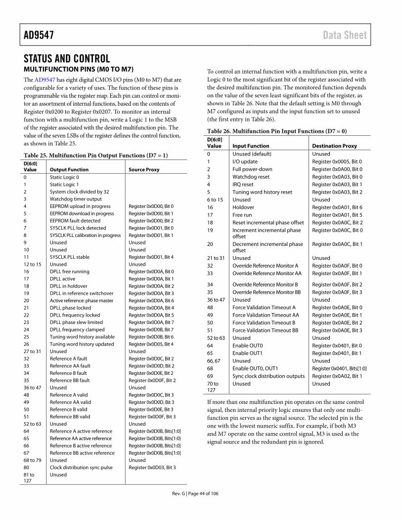
AD9547 Data Sheet
STATUS AND CONTROL MULTIFUNCTION PINS (M0 TO M7) The AD9547 has eight digital CMOS I/O pins (M0 to M7) that are configurable for a variety of uses. The function of these pins is programmable via the register map. Each pin can control or moni-tor an assortment of internal functions, based on the contents of Register 0x0200 to Register 0x0207. To monitor an internal function with a multifunction pin, write a Logic 1 to the MSB of the register associated with the desired multifunction pin. The value of the seven LSBs of the register defines the control function, as shown in Table 25.
Table 25. Multifunction Pin Output Functions (D7 = 1) D[6:0] Value Output Function Source Proxy
0 Static Logic 0 1 Static Logic 1 2 System clock divided by 32 3 Watchdog timer output 4 EEPROM upload in progress Register 0x0D00, Bit 0 5 EEPROM download in progress Register 0x0D00, Bit 1 6 EEPROM fault detected Register 0x0D00, Bit 2 7 SYSCLK PLL lock detected Register 0x0D01, Bit 0 8 SYSCLK PLL calibration in progress Register 0x0D01, Bit 1 9 Unused Unused 10 Unused Unused 11 SYSCLK PLL stable Register 0x0D01, Bit 4 12 to 15 Unused Unused 16 DPLL free running Register 0x0D0A, Bit 0 17 DPLL active Register 0x0D0A, Bit 1 18 DPLL in holdover Register 0x0D0A, Bit 2 19 DPLL in reference switchover Register 0x0D0A, Bit 3 20 Active reference: phase master Register 0x0D0A, Bit 6 21 DPLL phase locked Register 0x0D0A, Bit 4 22 DPLL frequency locked Register 0x0D0A, Bit 5 23 DPLL phase slew limited Register 0x0D0A, Bit 7 24 DPLL frequency clamped Register 0x0D0B, Bit 7 25 Tuning word history available Register 0x0D0B, Bit 6 26 Tuning word history updated Register 0x0D05, Bit 4 27 to 31 Unused Unused 32 Reference A fault Register 0x0D0C, Bit 2 33 Reference AA fault Register 0x0D0D, Bit 2 34 Reference B fault Register 0x0D0E, Bit 2 35 Reference BB fault Register 0x0D0F, Bit 2 36 to 47 Unused Unused 48 Reference A valid Register 0x0D0C, Bit 3 49 Reference AA valid Register 0x0D0D, Bit 3 50 Reference B valid Register 0x0D0E, Bit 3 51 Reference BB valid Register 0x0D0F, Bit 3 52 to 63 Unused Unused 64 Reference A active reference Register 0x0D0B, Bits[1:0] 65 Reference AA active reference Register 0x0D0B, Bits[1:0 66 Reference B active reference Register 0x0D0B, Bits[1:0] 67 Reference BB active reference Register 0x0D0B, Bits[1:0] 68 to 79 Unused Unused 80 Clock distribution sync pulse Register 0x0D03, Bit 3 81 to 127
Unused
To control an internal function with a multifunction pin, write a Logic 0 to the most significant bit of the register associated with the desired multifunction pin. The monitored function depends on the value of the seven least significant bits of the register, as shown in Table 26. Note that the default setting is M0 through M7 configured as inputs and the input function set to unused (the first entry in Table 26).
Table 26. Multifunction Pin Input Functions (D7 = 0) D[6:0] Value Input Function Destination Proxy 0 Unused (default) Unused 1 I/O update Register 0x0005, Bit 0 2 Full power-down Register 0x0A00, Bit 0 3 Watchdog reset Register 0x0A03, Bit 0 4 IRQ reset Register 0x0A03, Bit 1 5 Tuning word history reset Register 0x0A03, Bit 2 6 to 15 Unused Unused 16 Holdover Register 0x0A01, Bit 6 17 Free run Register 0x0A01, Bit 5 18 Reset incremental phase offset Register 0x0A0C, Bit 2 19 Increment incremental phase
offset Register 0x0A0C, Bit 0
20 Decrement incremental phase offset
Register 0x0A0C, Bit 1
21 to 31 Unused Unused 32 Override Reference Monitor A Register 0x0A0F, Bit 0 33 Override Reference Monitor AA Register 0x0A0F, Bit 1
34 Override Reference Monitor B Register 0x0A0F, Bit 2 35 Override Reference Monitor BB Register 0x0A0F, Bit 3 36 to 47 Unused Unused 48 Force Validation Timeout A Register 0x0A0E, Bit 0 49 Force Validation Timeout AA Register 0x0A0E, Bit 1 50 Force Validation Timeout B Register 0x0A0E, Bit 2 51 Force Validation Timeout BB Register 0x0A0E, Bit 3 52 to 63 Unused Unused 64 Enable OUT0 Register 0x0401, Bit 0 65 Enable OUT1 Register 0x0401, Bit 1 66, 67 Unused Unused 68 Enable OUT0, OUT1 Register 0x0401, Bits[1:0] 69 Sync clock distribution outputs Register 0x0A02, Bit 1 70 to 127
Unused Unused
If more than one multifunction pin operates on the same control signal, then internal priority logic ensures that only one multi-function pin serves as the signal source. The selected pin is the one with the lowest numeric suffix. For example, if both M3 and M7 operate on the same control signal, M3 is used as the signal source and the redundant pin is ignored.
Rev. G | Page 44 of 106
Data Sheet AD9547
At power-up, the multifunction pins can be used to force the device into certain configurations as defined in the Initial M0 to M7 Pin Programming section. This functionality, however, is valid only during power-up or following a reset, after which the pins can be reconfigured via the serial programming port or via the EEPROM.
IRQ PIN The AD9547 has a dedicated interrupt request (IRQ) pin. The IRQ pin output mode register (Register 0x0208, Bits[1:0]) controls how the IRQ pin asserts an interrupt based on the value of the two bits, as shown in Table 27.
Table 27. IRQ Pin Control—Register 0x0208, Bits[1:0] Setting Description 00 The IRQ pin is high impedance when deasserted and
active low when asserted and requires an external pull-up resistor (this is the default operating mode).
01 The IRQ pin is high impedance when deasserted and active high when asserted and requires an external pull-down resistor.
10 The IRQ pin is Logic 0 when deasserted and Logic 1 when asserted.
11 The IRQ pin is Logic 1 when deasserted and Logic 0 when asserted.
The AD9547 asserts the IRQ pin when any of the bits in the IRQ monitor registers (Address 0x0D02 to Address 0x0D09) are Logic 1. Each bit in these registers is associated with an internal function that is capable of producing an interrupt. Furthermore, each bit of the IRQ monitor register is the result of a logical AND of the associated internal interrupt signal and the corresponding bit in the IRQ mask register (Address 0x0209 to Address 0x0210). That is, the bits in the IRQ mask register have a one-to-one cor-respondence with the bits in the IRQ monitor register. When an internal function produces an interrupt signal and the associated IRQ mask bit is set, the corresponding bit in the IRQ monitor register is set.
The user should be aware that clearing a bit in the IRQ mask register removes only the mask associated with the internal interrupt signal. It does not clear the corresponding bit in the IRQ monitor register.
The IRQ pin is the result of a logical OR of all the IRQ monitor register bits. Thus, the AD9547 asserts the IRQ pin as long as any of the IRQ monitor register bits are Logic 1. Note that it is possible to have multiple bits set in the IRQ monitor register. Therefore, when the AD9547 asserts the IRQ pin, it may indicate an interrupt from several different internal functions. The IRQ monitor register provides the user with a means to interrogate the AD9547 to determine which internal function(s) produced the interrupt.
Typically, when the AD9547 asserts the IRQ pin, the user inter-rogates the IRQ monitor register to identify the source of the interrupt request. After servicing an indicated interrupt, the user should clear the associated IRQ monitor register bit via the IRQ clearing registers (Address 0x0A04 to Address 0x0A0B). The bits in the IRQ clearing register have a one-to-one correspondence with the bits in the IRQ monitor register. Note that the IRQ clearing register is autoclearing. The IRQ pin remains asserted until the user clears all of the bits in the IRQ monitor register that indicate an interrupt.
It is also possible to collectively clear all of the IRQ monitor register bits by setting the reset all IRQs bit in the reset functions register (Register 0x0A03, Bit 1). Note that this is an autoclearing bit. Setting this bit results in deassertion of the IRQ pin. Alter-natively, the user can program any of the multifunction pins to clear all IRQs. This allows the user to clear all IRQs by means of a hardware pin rather than by a serial I/O port operation.
Note that the IRQ function detects a state change in the function that is being monitored. However, if IRQs are cleared (or if they are enabled for the first time), an IRQ will not be generated for a pre-existing condition. The state must change after the IRQ is enabled. For example, if REFA is already invalid before a "REFA invalid" IRQ is enabled, an IRQ will not be generated.
WATCHDOG TIMER The watchdog timer is a general-purpose, programmable timer. To set its timeout period, the user writes to the 16-bit watchdog timer register (Address 0x0211 and Address 0x0212). A value of zero in this register disables the timer. A nonzero value sets the timeout period in units of milliseconds (ms), giving the watchdog timer a range of 1 ms to 65,535 ms. The relative accuracy of the timer is approximately 0.1% with an uncertainty of 0.5 ms.
If enabled, the timer runs continuously and generates a timeout event whenever the timeout period expires. The user has access to the watchdog timer status via the IRQ mechanism and the multifunction pins (M0 to M7). In the case of the multifunction pins, the timeout event of the watchdog timer is a pulse that lasts 32 system clock periods.
There are two ways to reset the watchdog timer (thereby pre-venting it from causing a timeout event). The first is by writing a Logic 1 to the autoclearing reset watchdog bit in the reset functions register (Register 0x0A03, Bit 0). Alternatively, the user can program any of the multifunction pins to reset the watchdog timer. This allows the user to reset the timer by means of a hardware pin rather than by a serial I/O port operation.
Rev. G | Page 45 of 106
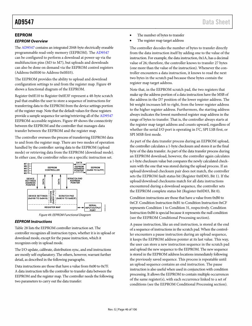
AD9547 Data Sheet
Rev. G | Page 46 of 106
EEPROM EEPROM Overview
The AD9547 contains an integrated 2048-byte electrically erasable programmable read-only memory (EEPROM). The AD9547 can be configured to perform a download at power-up via the multifunction pins (M3 to M7), but uploads and downloads can also be done on demand via the EEPROM control registers (Address 0x0E00 to Address 0x0E03).
The EEPROM provides the ability to upload and download configuration settings to and from the register map. Figure 49 shows a functional diagram of the EEPROM.
Register 0x0E10 to Register 0x0E3F represent a 48-byte scratch pad that enables the user to store a sequence of instructions for transferring data to the EEPROM from the device settings portion of the register map. Note that the default values for these registers provide a sample sequence for saving/retrieving all of the AD9547 EEPROM-accessible registers. Figure 49 shows the connectivity between the EEPROM and the controller that manages data transfer between the EEPROM and the register map.
The controller oversees the process of transferring EEPROM data to and from the register map. There are two modes of operation handled by the controller: saving data to the EEPROM (upload mode) or retrieving data from the EEPROM (download mode). In either case, the controller relies on a specific instruction set.
EEPROM(0x000 TO 0x7FF)
DA
TA
DA
TA
DATA
EEPROMADDRESSPOINTER
M7M6M5M4M3
REGISTER MAP
DEVICE SETTINGS(0x0100 TO 0x0A10)
SCRATCH PAD(0x0E10 TO 0x0E3F)
SERIALINPUT/OUTPUT
PORT
CO
ND
ITIO
N(0
x0E
01 [
4:0]
)
SCRATCH PADADDRESSPOINTER
DEVICESETTINGSADDRESSPOINTER
EEPROMCONTROLLER
0830
0-02
4
Figure 49. EEPROM Functional Diagram
EEPROM Instructions
Table 28 lists the EEPROM controller instruction set. The controller recognizes all instruction types, whether it is in upload or download mode, except for the pause instruction, which it recognizes only in upload mode.
The I/O update, calibrate, distribution sync, and end instructions are mostly self-explanatory. The others, however, warrant further detail, as described in the following paragraphs.
Data instructions are those that have a value from 0x00 to 0x7F. A data instruction tells the controller to transfer data between the EEPROM and the register map. The controller needs the following two parameters to carry out the data transfer:
The number of bytes to transfer The register map target address
The controller decodes the number of bytes to transfer directly from the data instruction itself by adding one to the value of the instruction. For example, the data instruction, 0x1A, has a decimal value of 26; therefore, the controller knows to transfer 27 bytes (one more than the value of the instruction). Whenever the con-troller encounters a data instruction, it knows to read the next two bytes in the scratch pad because these bytes contain the register map target address.
Note that, in the EEPROM scratch pad, the two registers that make up the address portion of a data instruction have the MSB of the address in the D7 position of the lower register address. The bit weight increases left to right, from the lower register address to the higher register address. Furthermore, the starting address always indicates the lowest numbered register map address in the range of bytes to transfer. That is, the controller always starts at the register map target address and counts upward, regardless of whether the serial I/O port is operating in I2C, SPI LSB first, or SPI MSB first mode.
As part of the data transfer process during an EEPROM upload, the controller calculates a 1-byte checksum and stores it as the final byte of the data transfer. As part of the data transfer process during an EEPROM download, however, the controller again calculates a 1-byte checksum value but compares the newly calculated check-sum with the one that was stored during the upload process. If an upload/download checksum pair does not match, the controller sets the EEPROM fault status bit (Register 0x0D03, Bit 1). If the upload/download checksums match for all data instructions encountered during a download sequence, the controller sets the EEPROM complete status bit (Register 0x0D03, Bit 0).
Condition instructions are those that have a value from 0xB0 to 0xCF. Condition Instruction 0xB1 to Condition Instruction 0xCF represents Condition 1 to Condition 31, respectively. Condition Instruction 0xB0 is special because it represents the null condition (see the EEPROM Conditional Processing section).
A pause instruction, like an end instruction, is stored at the end of a sequence of instructions in the scratch pad. When the control-ler encounters a pause instruction during an upload sequence, it keeps the EEPROM address pointer at its last value. This way, the user can store a new instruction sequence in the scratch pad and upload the new sequence to the EEPROM. The new sequence is stored in the EEPROM address locations immediately following the previously saved sequence. This process is repeatable until an upload sequence contains an end instruction. The pause instruction is also useful when used in conjunction with condition processing. It allows the EEPROM to contain multiple occurrences of the same register(s), with each occurrence linked to a set of conditions (see the EEPROM Conditional Processing section).
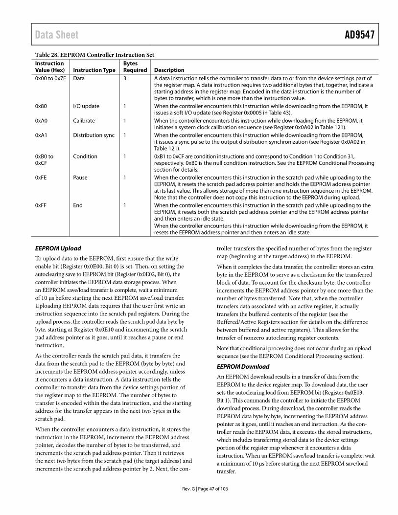
Data Sheet AD9547 Table 28. EEPROM Controller Instruction Set Instruction Value (Hex) Instruction Type
Bytes Required Description
0x00 to 0x7F Data 3 A data instruction tells the controller to transfer data to or from the device settings part of the register map. A data instruction requires two additional bytes that, together, indicate a starting address in the register map. Encoded in the data instruction is the number of bytes to transfer, which is one more than the instruction value.
0x80 I/O update 1 When the controller encounters this instruction while downloading from the EEPROM, it issues a soft I/O update (see Register 0x0005 in Table 43).
0xA0 Calibrate 1 When the controller encounters this instruction while downloading from the EEPROM, it initiates a system clock calibration sequence (see Register 0x0A02 in Table 121).
0xA1 Distribution sync 1 When the controller encounters this instruction while downloading from the EEPROM, it issues a sync pulse to the output distribution synchronization (see Register 0x0A02 in Table 121).
0xB0 to 0xCF
Condition 1 0xB1 to 0xCF are condition instructions and correspond to Condition 1 to Condition 31, respectively. 0xB0 is the null condition instruction. See the EEPROM Conditional Processing section for details.
0xFE Pause 1 When the controller encounters this instruction in the scratch pad while uploading to the EEPROM, it resets the scratch pad address pointer and holds the EEPROM address pointer at its last value. This allows storage of more than one instruction sequence in the EEPROM. Note that the controller does not copy this instruction to the EEPROM during upload.
0xFF End 1 When the controller encounters this instruction in the scratch pad while uploading to the EEPROM, it resets both the scratch pad address pointer and the EEPROM address pointer and then enters an idle state. When the controller encounters this instruction while downloading from the EEPROM, it resets the EEPROM address pointer and then enters an idle state.
EEPROM Upload
To upload data to the EEPROM, first ensure that the write enable bit (Register 0x0E00, Bit 0) is set. Then, on setting the autoclearing save to EEPROM bit (Register 0x0E02, Bit 0), the controller initiates the EEPROM data storage process. When an EEPROM save/load transfer is complete, wait a minimum of 10 µs before starting the next EEPROM save/load transfer. Uploading EEPROM data requires that the user first write an instruction sequence into the scratch pad registers. During the upload process, the controller reads the scratch pad data byte by byte, starting at Register 0x0E10 and incrementing the scratch pad address pointer as it goes, until it reaches a pause or end instruction.
As the controller reads the scratch pad data, it transfers the data from the scratch pad to the EEPROM (byte by byte) and increments the EEPROM address pointer accordingly, unless it encounters a data instruction. A data instruction tells the controller to transfer data from the device settings portion of the register map to the EEPROM. The number of bytes to transfer is encoded within the data instruction, and the starting address for the transfer appears in the next two bytes in the scratch pad.
When the controller encounters a data instruction, it stores the instruction in the EEPROM, increments the EEPROM address pointer, decodes the number of bytes to be transferred, and increments the scratch pad address pointer. Then it retrieves the next two bytes from the scratch pad (the target address) and increments the scratch pad address pointer by 2. Next, the con-
troller transfers the specified number of bytes from the register map (beginning at the target address) to the EEPROM.
When it completes the data transfer, the controller stores an extra byte in the EEPROM to serve as a checksum for the transferred block of data. To account for the checksum byte, the controller increments the EEPROM address pointer by one more than the number of bytes transferred. Note that, when the controller transfers data associated with an active register, it actually transfers the buffered contents of the register (see the Buffered/Active Registers section for details on the difference between buffered and active registers). This allows for the transfer of nonzero autoclearing register contents.
Note that conditional processing does not occur during an upload sequence (see the EEPROM Conditional Processing section).
EEPROM Download
An EEPROM download results in a transfer of data from the EEPROM to the device register map. To download data, the user sets the autoclearing load from EEPROM bit (Register 0x0E03, Bit 1). This commands the controller to initiate the EEPROM download process. During download, the controller reads the EEPROM data byte by byte, incrementing the EEPROM address pointer as it goes, until it reaches an end instruction. As the con-troller reads the EEPROM data, it executes the stored instructions, which includes transferring stored data to the device settings portion of the register map whenever it encounters a data instruction. When an EEPROM save/load transfer is complete, wait a minimum of 10 µs before starting the next EEPROM save/load transfer.
Rev. G | Page 47 of 106
AD9547 Data Sheet Note that conditional processing is applicable only when down-loading (see the EEPROM Conditional Processing section).
Automatic EEPROM Download
Following power-up, assertion of the RESET pin, or a soft reset (Register 0x0000, Bit 5 = 1), if FncInit[7:3] ≠ 0 (see the Initial M0 to M7 Pin Programming section), the instruction sequence stored in the EEPROM executes automatically with condition = FncInit[7:3]. In this way, a previously stored set of register values downloads automatically on power-up or with a hard or soft reset. See the EEPROM Conditional Processing section for details regarding conditional processing and the way that it modifies the download process.
Disabling Accidental Automatic EEPROM Download
It is possible to bypass EEPROM downloading when M3 to M7 are either accidentally left floating or are pulled high. The following steps ensure that EEPROM loading is bypassed:
1. Register 0x0E10 = 0xFF (end of data). 2. Register 0x0E00 = 0x01 (EEPROM write enable). 3. Register 0x0E02 = 0x01 (save to EEPROM). 4. Wait until Register 0xD00 equals 0x00.
EEPROM Conditional Processing
The condition instructions allow conditional execution of EEPROM instructions during a download sequence. During an upload sequence, however, they are stored as is and have no effect on the upload process.
Note that, during EEPROM downloads, the condition instructions themselves and the end instruction always execute unconditionally.
Conditional processing makes use of two elements: the condition (from Condition 1 to Condition 31) and the condition tag board. The relationships among the condition, the condition tag board, and the EEPROM controller appear schematically in Figure 50.
Condition is a 5-bit value with 32 possibilities. Condition = 0 is the null condition. When the null condition is in effect, the EEPROM controller executes all instructions unconditionally. The remaining 31 possibilities, condition = 1 through condition = 31, modify the EEPROM controller’s handling of a download sequence.
The condition originates from one of two sources (see Figure 50), as follows:
• FncInit, Bits[7:3], which is the state of multifunction pins M3 to M7 at power-up (see the Initial M0 to M7 Pin Programming section)
• Register 0x0E01, Bits[4:0]
If Register 0x0E01, Bits[4:0] ≠ 0, then the condition is the value stored in Register 0x0E01, Bits[4:0]; otherwise, the condition is FncInit, Bits[7:3]. Note that a nonzero condition that is present in Register 0x0E01, Bits[4:0] takes precedence over FncInit, Bits[7:3].
The condition tag board is a table that is maintained by the EEPROM controller. When the controller encounters a condition instruction, it decodes Condition Instruction 0xB1 through Condi-tion Instruction 0xCF as condition = 1 through condition = 31, respectively, and tags that particular condition in the condition tag board. However, Condition Instruction 0xB0 decodes as the null condition, for which the controller clears the condition tag board; subsequent download instructions execute unconditionally (until the controller encounters a new condition instruction).
During download, the EEPROM controller executes or skips instructions, depending on the value of the condition and the contents of the condition tag board. Note, however, that condition instructions and the end instruction always execute uncondi-tionally during download. If condition = 0, all instructions during download execute unconditionally. If condition ≠ 0 and there are any tagged conditions in the condition tag board, the controller executes instructions only if the condition is tagged.
Rev. G | Page 48 of 106

Data Sheet AD9547
Rev. G | Page 49 of 106
EXAMPLECONDITION 3 AND
CONDITION 13ARE TAGGED
EEPROM
EEPROM CONTROLLER
UPLOADPROCEDURE
CONDITIONHANDLER
DOWNLOADPROCEDURE
CONDITIONTAG BOARD
1 65432
111098
7
30 3124
2322212019181716
15141312
25 26 27 28 29
IF B1 ≤ INSTRUCTION ≤ CF,THEN TAG DECODED CONDITION
EXECUTE/SKIP
INSTRUCTION(S)
SCRATCHPAD
CONDITION
CONDITION = 0x0E01, BITS[4:0]ELSE CONDITION = FncInit, BITS[7:3]ENDIF
M7 M3
IF INSTRUCTION = B0,THEN CLEAR ALL TAGS
FncInit, BITS[7:3]REGISTER
0x0E01, BITS[4:0]
STORE CONDITIONINSTRUCTIONS AS
THEY ARE READ FROMTHE SCRATCH PAD.
WATCH FOROCCURRENCE OF
CONDITIONINSTRUCTIONS
DURINGDOWNLOAD.
IF NO TAGS OR CONDITION = 0 EXECUTE INSTRUCTIONSELSE IF CONDITION IS TAGGED EXECUTE INSTRUCTIONS ELSE SKIP INSTRUCTIONS ENDIFENDIF
5
5 5
IF 0x0E01, BITS[4:0] ≠ 0
Figure 50. EEPROM Conditional Processing
If the condition is not tagged, the controller skips instructions until it encounters a condition instruction that decodes as a tagged condition. Note that the condition tag board allows for multiple conditions to be tagged at any given moment. This conditional processing mechanism enables the user to have one download instruction sequence with many possible outcomes, depending on the value of the condition and the order in which the controller encounters the condition instructions.
Table 29 lists a sample EEPROM download instruction sequence. It illustrates the use of condition instructions and how they alter the download sequence. The table begins with the assumption that no conditions are in effect. That is, the most recently executed condition instruction is 0xB0, or no conditional instructions have been processed.
Table 29. EEPROM Conditional Processing Example Instruction Action 0x08 Transfer the system clock register contents
regardless of the current condition 0x01 0x00 0xB1 Tag Condition 1 0x19 Transfer the clock distribution register contents
only if condition = 1 0x04 0x00 0xB2 Tag Condition 2 0xB3 Tag Condition 3 0x07 Transfer the reference input register contents only
if condition = 1, 2, or 3 0x05 0x00 0x0A Calibrate the system clock only if condition = 1, 2,
or 3 0xB0 Clear the condition tag board
Instruction Action 0x80 Execute an I/O update, regardless of the value of
the condition 0x0A Calibrate the system clock, regardless of the value
of the condition
Storing Multiple Device Setups in EEPROM
Conditional processing makes it possible to create a number of different device setups, store them in EEPROM, and download a specific setup on demand. To do so, first pro-gram the device control registers for a specific setup. Then, store an upload sequence in the EEPROM scratch pad with the following general form:
1. Condition instruction (0xB1 to 0xCF) to identify the setup with a specific condition (1 to 31)
2. Data instructions (to save the register contents) along with any required calibrate and/or I/O update instructions
3. Pause instruction (0xFE)
With the upload sequence written to the scratch pad, perform an EEPROM upload (Register 0x0E02, Bit 0).
Reprogram the device control registers for the next desired setup. Then store a new upload sequence in the EEPROM scratch pad with the following general form:
1. Condition Instruction 0xB0 2. The next desired condition instruction (0xB1 to 0xCF, but
different from the one used during the previous upload to identify a new setup)
3. Data instructions (to save the register contents) along with any required calibrate and/or I/O update instructions
4. Pause instruction (FE)

AD9547 Data Sheet
With the upload sequence written to the scratch pad, perform an EEPROM upload (Register 0x0E02, Bit 0).
Repeat the process of programming the device control registers for a new setup, storing a new upload sequence in the EEPROM scratch pad (Step 1 through Step 4) and executing an EEPROM upload (Register 0x0E02, Bit 0) until all of the desired setups are uploaded to the EEPROM.
Note that, on the final upload sequence stored in the scratch pad, the pause instruction (FE) must be replaced with an end instruction (FF).
To download a specific setup on demand, first store the condition associated with the desired setup in Register 0x0E01, Bits[4:0]. Then perform an EEPROM download (Register 0x0E03, Bit 1). Alternatively, to download a specific setup at power-up, apply the required logic levels necessary to encode the desired condition on the M3 to M7 multifunction pins. Then power up the device, and an automatic EEPROM download occurs. The condition (as established by the M3 to M7 multifunction pins) guides the download sequence and results in a specific setup.
Keep in mind that the number of setups that can be stored in the EEPROM is limited. The EEPROM can hold a total of 2048 bytes.
Each nondata instruction requires one byte of storage. Each data instruction, however, requires N + 4 bytes of storage, where N is the number of transferred register bytes. The other four bytes include the data instruction itself (one byte), the target address (two bytes), and the checksum calculated by the EEPROM con-troller during the upload sequence (one byte).
Programming the EEPROM to Include a Clock Part ID
A special EEPROM loading sequence is required to use the clock part ID registers. These registers provide part and revision identification.
The default EEPROM loading sequence from Register 0x0E10 to Register 0x0E31 is unchanged. The following steps must be inserted into the EEPROM storage sequence to use the clock part ID registers:
1. Register 0x0E32 = 0x07 (write 8 bytes)2. Register 0x0E33 = 0x0C (at Register 0x0C00)3. Register 0x0E34 = 0x004. Register 0x0E35 = 0x80 (I/O update)5. Register 0x0E36 = 0xFF (end of data)
Rev. G | Page 50 of 106
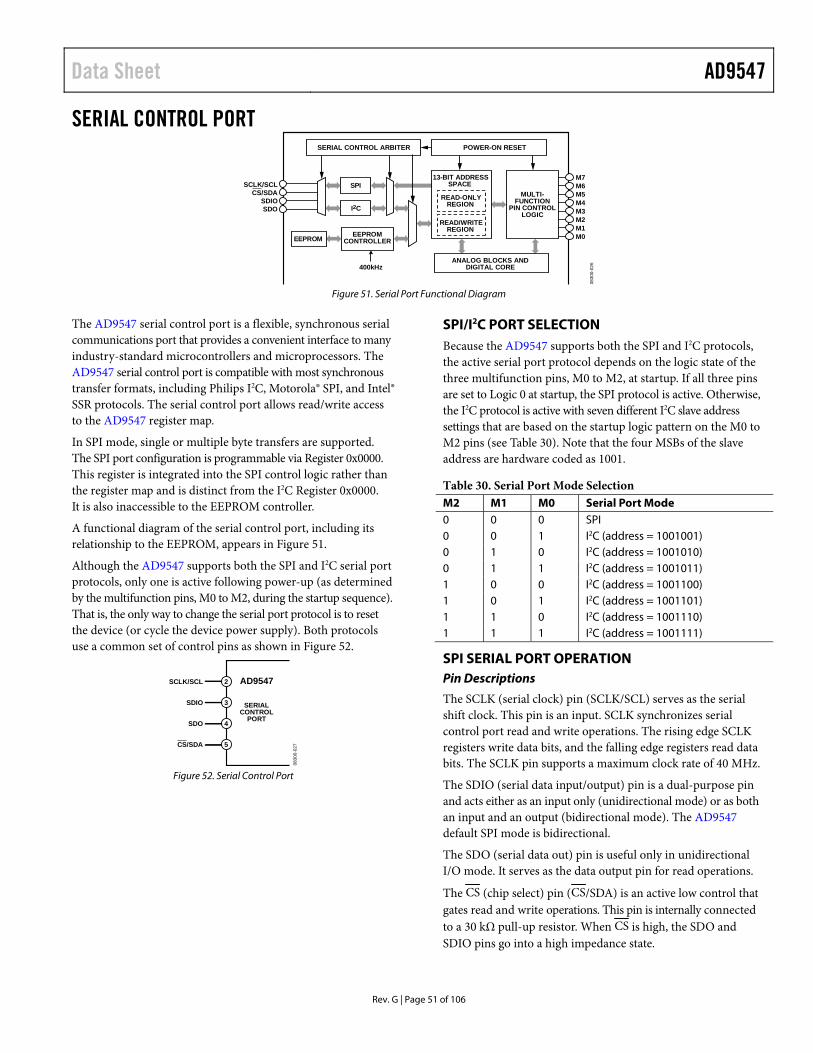
Data Sheet AD9547
Rev. G | Page 51 of 106
SERIAL CONTROL PORT
M7
M0M1M2M3M4M5M6
13-BIT ADDRESSSPACE
READ-ONLYREGION
READ/WRITEREGION
ANALOG BLOCKS ANDDIGITAL CORE
POWER-ON RESETSERIAL CONTROL ARBITER
SPI
I2C
EEPROMCONTROLLER
400kHz
MULTI-FUNCTION
PIN CONTROLLOGIC
SCLK/SCLCS/SDA
SDIOSDO
EEPROM
0830
0-02
6
Figure 51. Serial Port Functional Diagram
The AD9547 serial control port is a flexible, synchronous serial communications port that provides a convenient interface to many industry-standard microcontrollers and microprocessors. The AD9547 serial control port is compatible with most synchronous transfer formats, including Philips I2C, Motorola® SPI, and Intel® SSR protocols. The serial control port allows read/write access to the AD9547 register map.
In SPI mode, single or multiple byte transfers are supported. The SPI port configuration is programmable via Register 0x0000. This register is integrated into the SPI control logic rather than the register map and is distinct from the I2C Register 0x0000. It is also inaccessible to the EEPROM controller.
A functional diagram of the serial control port, including its relationship to the EEPROM, appears in Figure 51.
Although the AD9547 supports both the SPI and I2C serial port protocols, only one is active following power-up (as determined by the multifunction pins, M0 to M2, during the startup sequence). That is, the only way to change the serial port protocol is to reset the device (or cycle the device power supply). Both protocols use a common set of control pins as shown in Figure 52.
AD9547SCLK/SCL
CS/SDA
SDO
SDIO
2
5
4
3 SERIALCONTROL
PORT
0830
0-02
7
Figure 52. Serial Control Port
SPI/I2C PORT SELECTION Because the AD9547 supports both the SPI and I2C protocols, the active serial port protocol depends on the logic state of the three multifunction pins, M0 to M2, at startup. If all three pins are set to Logic 0 at startup, the SPI protocol is active. Otherwise, the I2C protocol is active with seven different I2C slave address settings that are based on the startup logic pattern on the M0 to M2 pins (see Table 30). Note that the four MSBs of the slave address are hardware coded as 1001.
Table 30. Serial Port Mode Selection M2 M1 M0 Serial Port Mode 0 0 0 SPI 0 0 1 I2C (address = 1001001) 0 1 0 I2C (address = 1001010) 0 1 1 I2C (address = 1001011) 1 0 0 I2C (address = 1001100) 1 0 1 I2C (address = 1001101) 1 1 0 I2C (address = 1001110) 1 1 1 I2C (address = 1001111)
SPI SERIAL PORT OPERATION Pin Descriptions
The SCLK (serial clock) pin (SCLK/SCL) serves as the serial shift clock. This pin is an input. SCLK synchronizes serial control port read and write operations. The rising edge SCLK registers write data bits, and the falling edge registers read data bits. The SCLK pin supports a maximum clock rate of 40 MHz.
The SDIO (serial data input/output) pin is a dual-purpose pin and acts either as an input only (unidirectional mode) or as both an input and an output (bidirectional mode). The AD9547 default SPI mode is bidirectional.
The SDO (serial data out) pin is useful only in unidirectional I/O mode. It serves as the data output pin for read operations.
The CS (chip select) pin (CS/SDA) is an active low control that gates read and write operations. This pin is internally connected to a 30 kΩ pull-up resistor. When CS is high, the SDO and SDIO pins go into a high impedance state.

AD9547 Data Sheet SPI Mode Operation
The SPI port supports both 3-wire (bidirectional) and 4-wire (unidirectional) hardware configurations and both MSB-first and LSB-first data formats. Both the hardware configuration and data format features are programmable. By default, the AD9547 uses the bidirectional MSB-first mode. The bidirectional mode is the default mode so that the user can still write to the device to switch to unidirectional mode, if it is wired for unidirectional operation.
Assertion (active low) of the CS pin initiates a write or read operation to the AD9547 SPI port. For data transfers of three bytes or fewer (excluding the instruction word), the device supports the CS stalled high mode (see Table 31). In this mode, the CS pin can be temporarily deasserted on any byte boundary, allowing time for the system controller to process the next byte. CS can be deasserted only on byte boundaries, however. This applies to both the instruction and data portions of the transfer.
Table 31. Byte Transfer Count W1 W0 Bytes to Transfer 0 0 1 0 1 2 1 0 3 1 1 Streaming mode
During stall high periods, the serial control port state machine enters a wait state until all data is sent. If the system controller decides to abort a transfer midstream, the state machine must be reset either by completing the transfer or by asserting the CS pin for at least one complete SCLK cycle (but less than eight SCLK cycles). Deasserting the CS pin on a nonbyte boundary terminates the serial transfer and flushes the buffer.
In streaming mode (see Table 31), any number of data bytes can be transferred in a continuous stream. The register address is automatically incremented or decremented. CS must be deas-serted at the end of the last byte transferred, thereby ending the stream mode.
Communication Cycle—Instruction Plus Data
The SPI protocol consists of a two-part communication cycle. The first part is a 16-bit instruction word that is coincident with the first 16 SCLK rising edges and a payload. The instruction word provides the AD9547 serial control port with information regard-ing the payload. The instruction word includes the R/W bit that indicates the direction of the payload transfer (that is, a read or write operation). The instruction word also indicates the number of bytes in the payload and the starting register address of the first payload byte.
Write
If the instruction word indicates a write operation, the payload is written into the serial control port buffer of the AD9547. Data bits are registered on the rising edge of SCLK. The length of the transfer (1, 2, or 3 bytes or streaming mode) depends on the W0 and W1 bits (see Table 31) in the instruction byte. When not streaming, CS can be deasserted after each sequence of eight bits to stall the bus (except after the last byte, where it ends the cycle). When the bus is stalled, the serial transfer resumes when CS is asserted. Deasserting the CS pin on a nonbyte boundary resets the serial control port. Reserved or blank registers are not skipped over automatically during a write sequence. Therefore, the user must know what bit pattern to write to the reserved registers to preserve proper operation of the part. Generally, it does not matter what data is written to blank registers, but it is customary to write 0s.
Most of the serial port registers are buffered. Refer to the Buffered/Active Registers section for details on the difference between buffered and active registers. Therefore, data written into buffered registers does not immediately take effect. An addi-tional operation is needed to transfer buffered serial control port contents to the registers that actually control the device. This is accomplished with an I/O update operation that is performed in one of two ways: by writing a Logic 1 to Register 0x0005, Bit 0 (this bit is self-clearing) or by using an external signal via an appropriately programmed multifunction pin. The user can change as many register bits as desired before executing an I/O update. The I/O update operation transfers the buffer register contents to their active register counterparts.
Read
The AD9547 supports the long instruction mode only. If the instruction word indicates a read operation, the next N × 8 SCLK cycles clock out the data from the address specified in the instruction word. N is the number of data bytes read and depends on the W0 and W1 bits of the instruction word.
During a SPI read, serial data on SDIO (or SDO in the case of 4-wire mode) transitions on the SCLK falling edge, and is normally sampled on the SCLK rising edge. To read the last bit correctly, the SPI host must be able to tolerate a zero hold time. If zero hold time is not possible, the user can either use streaming mode and delay the rising edge of CS, or sample the serial data on the SCLK falling edge. However, to correctly sample the data on the SCLK falling edge, the user must ensure that the setup time is greater than tDV (time data valid). Blank registers are not skipped over during readback.
A readback operation takes data from either the serial control port buffer registers or the active registers, as determined by Register 0x0004, Bit 0.
Rev. G | Page 52 of 106
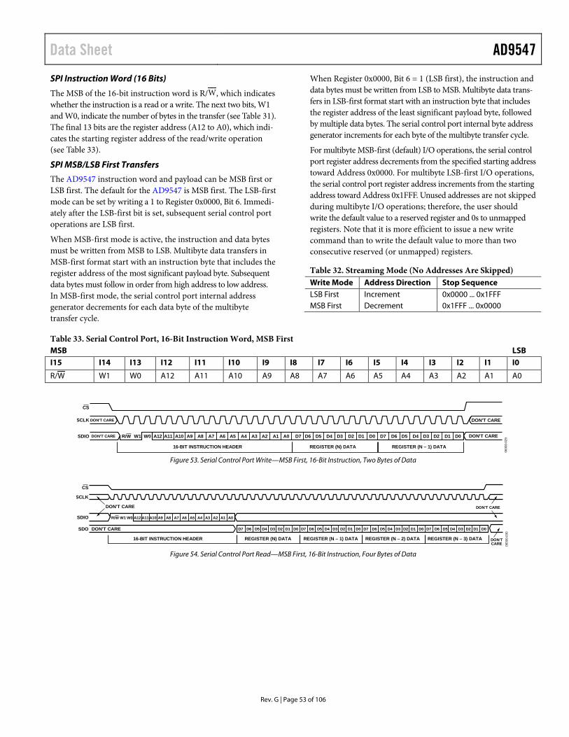
Data Sheet AD9547 SPI Instruction Word (16 Bits)
The MSB of the 16-bit instruction word is R/W, which indicates whether the instruction is a read or a write. The next two bits, W1 and W0, indicate the number of bytes in the transfer (see Table 31). The final 13 bits are the register address (A12 to A0), which indi-cates the starting register address of the read/write operation (see Table 33).
SPI MSB/LSB First Transfers
The AD9547 instruction word and payload can be MSB first or LSB first. The default for the AD9547 is MSB first. The LSB-first mode can be set by writing a 1 to Register 0x0000, Bit 6. Immedi-ately after the LSB-first bit is set, subsequent serial control port operations are LSB first.
When MSB-first mode is active, the instruction and data bytes must be written from MSB to LSB. Multibyte data transfers in MSB-first format start with an instruction byte that includes the register address of the most significant payload byte. Subsequent data bytes must follow in order from high address to low address. In MSB-first mode, the serial control port internal address generator decrements for each data byte of the multibyte transfer cycle.
When Register 0x0000, Bit 6 = 1 (LSB first), the instruction and data bytes must be written from LSB to MSB. Multibyte data trans-fers in LSB-first format start with an instruction byte that includes the register address of the least significant payload byte, followed by multiple data bytes. The serial control port internal byte address generator increments for each byte of the multibyte transfer cycle.
For multibyte MSB-first (default) I/O operations, the serial control port register address decrements from the specified starting address toward Address 0x0000. For multibyte LSB-first I/O operations, the serial control port register address increments from the starting address toward Address 0x1FFF. Unused addresses are not skipped during multibyte I/O operations; therefore, the user should write the default value to a reserved register and 0s to unmapped registers. Note that it is more efficient to issue a new write command than to write the default value to more than two consecutive reserved (or unmapped) registers.
Table 32. Streaming Mode (No Addresses Are Skipped) Write Mode Address Direction Stop Sequence LSB First Increment 0x0000 ... 0x1FFF MSB First Decrement 0x1FFF ... 0x0000
Table 33. Serial Control Port, 16-Bit Instruction Word, MSB First MSB LSB I15 I14 I13 I12 I11 I10 I9 I8 I7 I6 I5 I4 I3 I2 I1 I0
R/W W1 W0 A12 A11 A10 A9 A8 A7 A6 A5 A4 A3 A2 A1 A0
CS
SCLK DON'T CARE
SDIO A12W0W1R/W A11 A10 A9 A8 A7 A6 A5 A4 A3 A2 A1 A0 D7 D6 D5 D4 D3 D2 D1 D0 D7 D6 D5 D4 D3 D2 D1 D0 DON'T CAREDON'T CARE
DON'T CARE
16-BIT INSTRUCTION HEADER REGISTER (N) DATA REGISTER (N – 1) DATA
0830
0-02
9
Figure 53. Serial Control Port Write—MSB First, 16-Bit Instruction, Two Bytes of Data
CS
SCLK
SDIO
SDO
REGISTER (N) DATA16-BIT INSTRUCTION HEADER REGISTER (N – 1) DATA REGISTER (N – 2) DATA REGISTER (N – 3) DATA
A12W0W1R/W A11 A10 A9 A8 A7 A6 A5 A4 A3 A2 A1 A0
DON'T CAREDON'T CARE
DON'T CARE
DON'TCARE
D7 D6 D5 D4 D3 D2 D1 D0 D7 D6 D5 D4 D3 D2 D1 D0 D7 D6 D5 D4 D3 D2 D1 D0 D7 D6 D5 D4 D3 D2 D1 D0
0830
0-03
0
Figure 54. Serial Control Port Read—MSB First, 16-Bit Instruction, Four Bytes of Data
Rev. G | Page 53 of 106
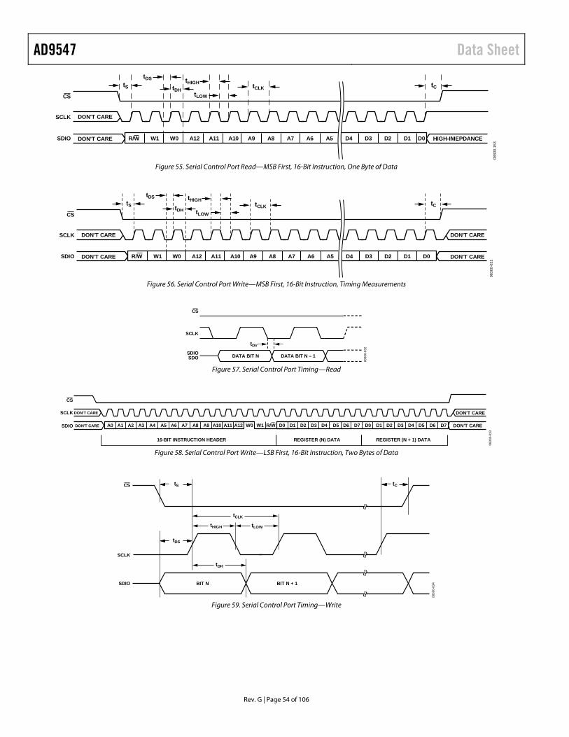
AD9547 Data Sheet
Rev. G | Page 54 of 106
tS
DON'T CARE
DON'T CARE W1 W0 A12 A11 A10 A9 A8 A7 A6 A5 D4 D3 D2 D1 D0 HIGH-IMEPDANCER/W
tDS
tDH
tHIGH
tLOW
tCLK tC
CS
SCLK
SDIO
0830
0-15
3
Figure 55. Serial Control Port Read—MSB First, 16-Bit Instruction, One Byte of Data
tS
DON'T CARE
DON'T CARE W1 W0 A12 A11 A10 A9 A8 A7 A6 A5 D4 D3 D2 D1 D0
DON'T CARE
DON'T CARER/W
tDS
tDH
tHIGH
tLOW
tCLK tC
CS
SCLK
SDIO
0830
0-03
1
Figure 56. Serial Control Port Write—MSB First, 16-Bit Instruction, Timing Measurements
DATA BIT N – 1DATA BIT N
CS
SCLK
SDIOSDO
tDV
0830
0-03
2
Figure 57. Serial Control Port Timing—Read
CS
SCLK DON'T CARE DON'T CARE
16-BIT INSTRUCTION HEADER REGISTER (N) DATA REGISTER (N + 1) DATA
SDIO DON'T CAREDON'T CARE A0 A1 A2 A3 A4 A5 A6 A7 A8 A9 A10 A11 A12 D1D0R/WW1W0 D2 D3 D4 D5 D6 D7 D0 D1 D2 D3 D4 D5 D6 D7
0830
0-03
3
Figure 58. Serial Control Port Write—LSB First, 16-Bit Instruction, Two Bytes of Data
CS
SCLK
SDIO
tHIGH tLOW
tCLK
tS
tDS
tDH
tC
BIT N BIT N + 1
0830
0-03
4
Figure 59. Serial Control Port Timing—Write

Data Sheet AD9547
Table 34. Serial Control Port Timing Parameter Description tDS Setup time between data and the rising edge of SCLK. tDH Hold time between data and the rising edge of SCLK. tCLK Period of the clock. tS Setup time between the CS falling edge and SCLK rising edge (start of the communication cycle).
tC Setup time between the SCLK rising edge and the CS rising edge (end of the communication cycle). To ensure that SDIO/SDO do not tristate before the last data bit (D0) is read, it is recommended that a ½ SCLK cycle be used for tc.
tHIGH Minimum period that SCLK should be in a logic high state. tLOW Minimum period that SCLK should be in a logic low state. tDV SCLK to valid SDIO and SDO (see Figure 57).
Rev. G | Page 55 of 106

AD9547 Data Sheet
Rev. G | Page 56 of 106
I2C SERIAL PORT OPERATION The I2C interface has the advantage of requiring only two control pins and is a de facto standard throughout the I2C industry. However, its disadvantage is programming speed, which is 400 kbps maximum. The AD9547 I2C port design is based on the I2C fast mode standard from Philips, so it supports both the 100 kHz standard mode and the 400 kHz fast mode. Fast mode imposes a glitch tolerance requirement on the control signals; that is, the input receivers ignore pulses of less than 50 ns duration.
The AD9547 I2C port consists of a serial data line (SDA) and a serial clock line (SCL). In an I2C bus system, the AD9547 is connected to the serial bus (data bus SDA and clock bus SCL) as a slave device; that is, no clock is generated by the AD9547. The AD9547 uses direct 16-bit memory addressing instead of traditional 8-bit memory addressing.
The AD9547 allows for up to seven unique slave devices to occupy the I2C bus. These are accessed via a 7-bit slave address that is transmitted as part of an I2C packet. Only the device with a match-ing slave address responds to subsequent I2C commands. The device slave address is 1001xxx (the last three bits are determined by the M0 to M2 pins). The four MSBs (1001) are hardwired, whereas the three LSBs (xxx, determined by the M0 to M2 pins) are programmable via the power-up state of the multifunction pins (see the Initial M0 to M7 Pin Programming section).
I2C Bus Characteristics
A summary of the various I2C protocols appears in Table 35.
Table 35. I2C Bus Abbreviation Definitions Abbreviation Definition
S Start
Sr Repeated start
P Stop
A Acknowledge
A No acknowledge
W Write
R Read
The transfer of data appears graphically in Figure 60. One clock pulse is generated for each data bit transferred. The data on the SDA line must be stable during the high period of the clock. The high or low state of the data line can change only when the clock signal on the SCL line is low.
DATA LINESTABLE;
DATA VALID
CHANGEOF DATA
ALLOWED
SDA
SCL
0830
0-03
5
Figure 60. Valid Bit Transfer
Start/stop functionality appears graphically in Figure 61. The start condition is characterized by a high-to-low transition on the SDA line while SCL is high. The start condition is always generated by the master to initialize data transfer. The stop condition is characterized by a low-to-high transition on the SDA line while SCL is high. The stop condition is always generated by the master to terminate data transfer.
SDA
START CONDITION STOP CONDITION
SCLS P
0830
0-03
6
Figure 61. Start and Stop Condition
Every byte on the SDA line must be eight bits long. Each byte must be followed by an acknowledge bit. Bytes are sent MSB first.
The acknowledge bit (A) is the ninth bit attached to any 8-bit data byte. An acknowledge bit is always generated by the receiving device (receiver) to inform the transmitter that the byte has been received. It is done by pulling the SDA line low during the ninth clock pulse after each 8-bit data byte.
The no acknowledge bit (A) is the ninth bit attached to any 8-bit data byte. A no acknowledge bit is always generated by the receiving device (receiver) to inform the transmitter that the byte has not been received. It is done by leaving the SDA line high during the ninth clock pulse after each 8-bit data byte.
1 2 8 9 1 2 3 TO 73 TO 7 8 9 10
SDA
SCLS
MSB
ACK FROMSLAVE RECEIVER
ACK FROMSLAVE RECEIVER
P
0830
0-03
7
Figure 62. Acknowledge Bit

Data Sheet AD9547
Rev. G | Page 57 of 106
Data Transfer Process
The master initiates data transfer by asserting a start condition. This indicates that a data stream follows. All I2C slave devices connected to the serial bus respond to the start condition.
The master then sends an 8-bit address byte over the SDA line, consisting of a 7-bit slave address (MSB first) plus an R/W bit. This bit determines the direction of the data transfer, that is, whether data is written to or read from the slave device (0 = write, 1 = read).
The peripheral whose address corresponds to the transmitted address responds by sending an acknowledge bit. All other devices on the bus remain idle while the selected device waits for data to be read from or written to it. If the R/W bit = 0, the master (trans-mitter) writes to the slave device (receiver). If the R/W bit = 1, the master (receiver) reads from the slave device (transmitter). See the Data Transfer Format section for the command format.
Data is then sent over the serial bus in the format of nine clock pulses, one data byte (eight bits) from either master (write mode) or slave (read mode) followed by an acknowledge bit from the receiving device. The number of bytes that can be transmitted per transfer is unrestricted. In write mode, the first two data
bytes immediately after the slave address byte are the internal memory (control registers) address bytes with the high address byte first. This addressing scheme gives a memory address up to 216 − 1 = 65,535. The data bytes after these two memory address bytes are register data written into or read from the control regi-sters. In read mode, the data bytes after the slave address byte are register data written into or read from the control registers.
When all data bytes are read or written, stop conditions are estab-lished. In write mode, the master (transmitter) asserts a stop condition to end data transfer during the 10th clock pulse following the acknowledge bit for the last data byte from the slave device (receiver). In read mode, the master device (receiver) receives the last data byte from the slave device (transmitter) but does not pull SDA low during the ninth clock pulse. This is known as a no acknowledge bit. When receiving the no acknowledge bit, the slave device knows the data transfer is finished and enters idle mode. The master then takes the data line low during the low period before the 10th clock pulse, and high during the 10th clock pulse to assert a stop condition.
A start condition can be used in place of a stop condition. Furthermore, a start or stop condition can occur at any time, and partially transferred bytes are discarded.
1 2 8 9 1 2 3 TO 73 TO 7 8 9 10
ACK FROMSLAVE RECEIVER
ACK FROMSLAVE RECEIVER
SDA
SCLS
MSB
P
0830
0-03
8
Figure 63. Data Transfer Process (Master Write Mode, 2-Byte Transfer Used for Illustration)
1 2 8 9 1 2 3 TO 73 TO 7 8 9 10
ACK FROMMASTER RECEIVER
NO ACK FROMMASTER RECEIVER
SDA
SCLS P
0830
0-03
9
Figure 64. Data Transfer Process (Master Read Mode, 2-Byte Transfer Used for Illustration)
Data Transfer Format
In write byte format, the write byte protocol is used to write a register address to the RAM starting from the specified RAM address.
S Slave Address
W A RAM Address High Byte
A RAM Address Low Byte
A RAM Data 0
A RAM Data 1
A RAM Data 2
A P
In send byte format, the send byte protocol is used to set up the register address for subsequent reads.
S Slave Address W A RAM Address High Byte A RAM Address Low Byte A P
In receive byte format, the receive byte protocol is used to read the data bytes from RAM starting from the current address.
S Slave Address R A RAM Data 0 A RAM Data 1 A RAM Data 2 A P
Read byte format combines the format of the send byte and the receive byte formats.
S Slave Address
W A RAM Address
High Byte
A RAM Address
Low Byte
A Sr Slave Address
R A RAM Data
0
A RAM Data
1
A RAM Data
2
A P
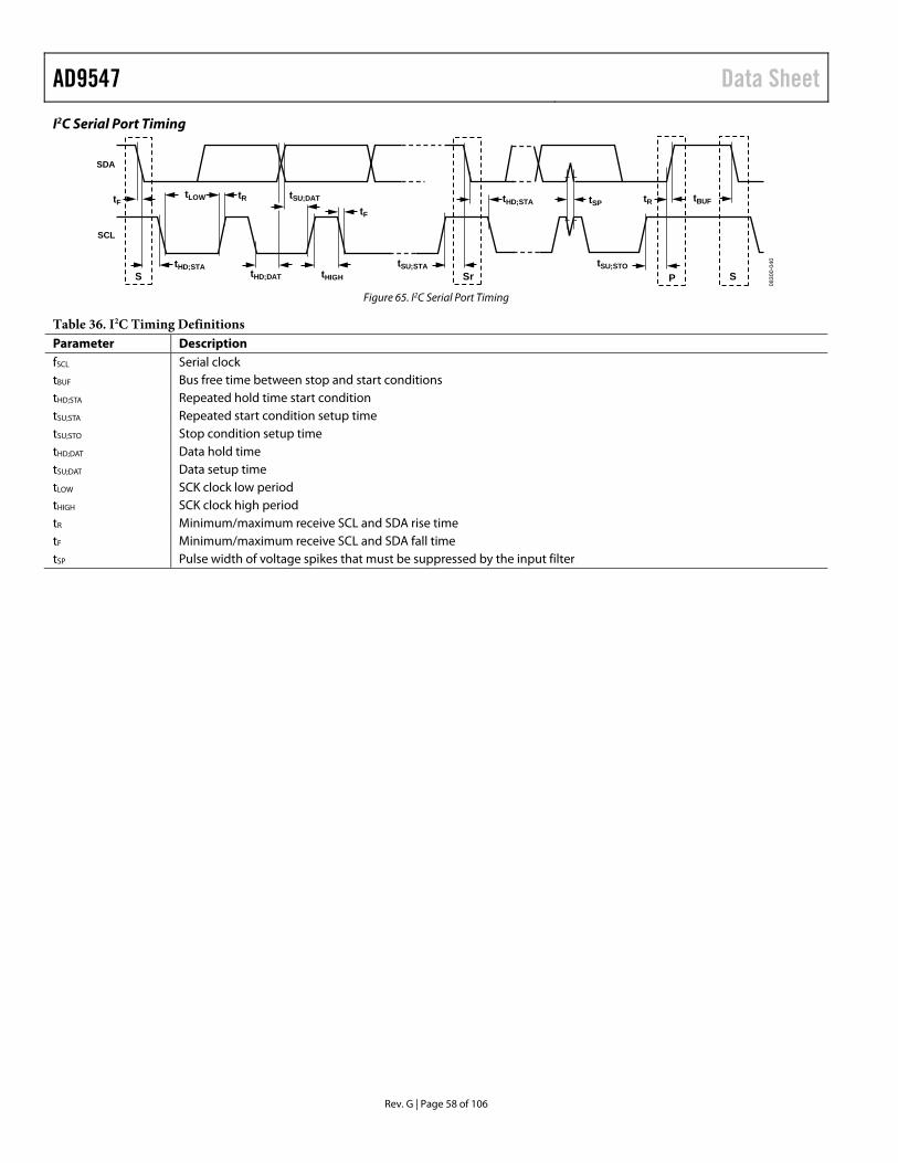
AD9547 Data Sheet
Rev. G | Page 58 of 106
I2C Serial Port Timing
S Sr SP
SDA
SCL
tSPtHD;STA
tSU;STA
tSU;DAT
tHD;DATtHD;STA
tHIGH
tLOW
tSU;STO
tBUFtRtF
tRtF
0830
0-04
0
Figure 65. I2C Serial Port Timing
Table 36. I2C Timing Definitions Parameter Description fSCL Serial clock tBUF Bus free time between stop and start conditions tHD;STA Repeated hold time start condition tSU;STA Repeated start condition setup time tSU;STO Stop condition setup time tHD;DAT Data hold time tSU;DAT Data setup time tLOW SCK clock low period tHIGH SCK clock high period tR Minimum/maximum receive SCL and SDA rise time tF Minimum/maximum receive SCL and SDA fall time tSP Pulse width of voltage spikes that must be suppressed by the input filter

Data Sheet AD9547
Rev. G | Page 59 of 106
I/O PROGRAMMING REGISTERS The register map spans an address range from 0x0000 through 0x0E3F (0 to 3647, decimal). Each address provides access to one byte (eight bits) of data. Each individual register is identified by its four-digit hexadecimal address (for example, Register 0x0A10). In some cases, a group of addresses collectively define a register (for example, the IRQ mask register consists of Register 0x0209, Register 0x020A, Register 0x020B, Register 0x020C, Register 0x020D, Register 0x020E, Register 0x020F, and Register 0x0210).
In general, when a group of registers defines a control parameter, the LSB of the value resides in the D0 position of the register with the lowest address. The bit weight increases from right to left, from the lowest register address to the highest register address. For example, the default value of the incremental phase lock offset step size register (Address 0x0314 to Address 0x0315) is the 16-bit hexadecimal number, 0x03E8 (not 0xE803). Note that the EEPROM storage sequence registers (Address 0x0E10 to Address 0x0E3F) are an exception to this convention (see the EEPROM Instructions section).
BUFFERED/ACTIVE REGISTERS There are two broad categories of registers on the AD9547; buffered and active (see Figure 66). Buffered registers need an I/O update to apply their contents to the internal device functions. In contrast, active registers do not require an I/O update to transfer data between the buffered registers and the internal device functions. In operation, the user programs as many buffered registers as desired and then issues an I/O update. The I/O update is performed by writing to Register 0x0005, Bit 0 = 1 (or by the external application of the necessary logic level to one of the multifunction pins previously programmed as an I/O update input). The contents of the buffered registers that are connected directly to the internal device functions affect those functions immediately. The contents of buffered registers that connect to active registers do not affect the internal device functions until the I/O update event occurs. An L in the Opt column of the register map indicates an active (or live) register. An S or a C in the Opt column of the register map identifies a buffered register. An S entry means that the I/O update signal to the active register is synchronized with the serial port clock or with an input signal driving one of the multifunction pins. On the other hand, a C entry means that the I/O update signal to the active register is synchronized with a clock signal derived from the internal system clock (fS/32), as shown in Figure 66.
When reading back a register that has both buffered and active contents, Register 0x0004, Bit 0 can be used to select whether to read back the buffered or active contents. Read-back of the active contents occurs when Register 0x0004, Bit 0= 0, whereas readback of the buffered contents occurs when Register 0x0004, Bit 0 = 1. Note that a read-only active register requires an I/O update before its contents can be read.
AC
TIVE
CR
EGIS
TER
SA
CTI
VE S
REG
ISTE
RS
I/O U
PDA
TE
TO IN
TER
NA
L D
EVIC
E FU
NC
TIO
NS
BUF
FER
EDRE
GIS
TERS
FROMMULTIFUNCTION
PIN LOGIC
SERIALCONTROL
PORT
fS/32
EDGEDETECT
CS/SDA
SCLK/SCL
SDIO
SDO
5
3
4
2
0830
0-04
1
Figure 66. Buffered and Active Registers
AUTOCLEARING REGISTERS An A in the Opt column of the register map identifies an auto-clearing register. Typically, the active value for an autoclearing register takes effect following an I/O update. The bit is cleared by the internal device logic upon completion of the prescribed action.
REGISTER ACCESS RESTRICTIONS Read and write access to the registers may be restricted, depending on the register in question, the source and direction of access, and the current state of the device. Each register can be classified into one or more access types. When more than one type applies, the most restrictive condition that applies at that time is used.
When access is denied to a register, all attempts to read the register return a 0 byte, and all attempts to write to the register are ignored. Access to nonexistent registers is handled in the same way as for a denied register.
Regular Access
Registers with regular access do not fall into any other category. Both read and write access to registers of this type can be from the serial port or the EEPROM controller. However, only one of these sources can have access to a register at any given time (access is mutually exclusive). When the EEPROM controller is active, either in load or store mode, it has exclusive access to the registers.
Read-Only Access
An R in the Opt column of the register map identifies read-only registers. Access is available at all times, including when the EEPROM controller is active.
Exclusion from EEPROM Access
An E in the Opt column of the register map identifies a register with contents that are inaccessible to the EEPROM. That is, the contents of this type of register cannot be transferred directly to the EEPROM or vice versa. Note that read-only registers (R) are inaccessible to the EEPROM, as well.
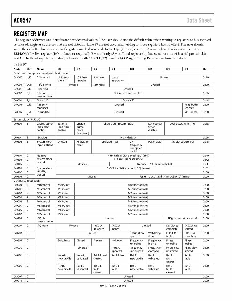
AD9547 Data Sheet
REGISTER MAP The register addresses and defaults are hexadecimal values. The user should use the default value when writing to registers or bits marked as unused. Register addresses that are not listed in Table 37 are not used, and writing to those registers has no effect. The user should write the default value to sections of registers marked reserved. In the Opt (Option) column, A = autoclear; E = inaccessible to the EEPROM; L = live register (I/O update not required); R = read only; S = buffered register (update synchronous with serial port clock); and C = buffered register (update synchronous with SYSCLK/32). See the I/O Programming Registers section for details.
Table 37. Addr Opt1 Name D7 D6 D5 D4 D3 D2 D1 D0 Def
Serial port configuration and part identification
0x0000 L, E SPI control Unidirec-tional
LSB first/ IncAddr
Soft reset Long instruction
Unused 0x10
0x0000 Dup I2C control Unused Soft reset Unused 0x00
0x0001 L, E Reserved Unused
0x0002 R, L Silicon revision level
Silicon revision number 0xF6
0x0003 R, L Device ID Device ID 0x48
0x0004 L, E Register readback
Unused Read buffer register
0x00
0x0005 L, A, E
I/O update Unused I/O update 0x00
System clock (SYSCLK)
0x0100 S Charge pump/ lock detect control
External loop filter enable
Charge pump mode (auto/man)
Charge pump current[2:0] Lock detect timer disable
Lock detect timer[1:0] 0x18
0x0101 S N divider N divider[7:0] 0x28
0x0102 S System clock input options
Unused M divider reset
M divider[1:0] 2× frequency multiplier enable
PLL enable SYSCLK source[1:0] 0x45
0x0103 C Nominal system clock period
Nominal SYSCLK period[15:0] (in fs) (1 ns at 1 ppm accuracy)
0x40
0x0104 C 0x42
0x0105 C Unused Nominal SYSCLK period[20:16] 0x0F
0x0106 C System clock stability period
SYSCLK stability period[15:0] (in ms) 0x01
0x0107 C 0x00
0x0108 C Unused System clock stability period[19:16] (in ms) 0x00
General configuration
0x0200 S M0 control M0 in/out M0 function[6:0] 0x00
0x0201 S M1 control M1 in/out M1 function[6:0] 0x00
0x0202 S M2 control M2 in/out M2 function[6:0] 0x00
0x0203 S M3 control M3 in/out M3 function[6:0] 0x00
0x0204 S M4 control M4 in/out M4 function[6:0] 0x00
0x0205 S M5 control M5 in/out M5 function[6:0] 0x00
0x0206 S M6 control M6 in/out M6 function[6:0] 0x00
0x0207 S M7 control M7 in/out M7 function[6:0] 0x00
0x0208 C IRQ pin output mode
Unused IRQ pin output mode[1:0] 0x00
0x0209 C IRQ mask Unused SYSCLK unlocked
SYSCLK locked
Unused SYSCLK cal complete
SYSCLK cal started
0x00
0x020A C Unused Distribution sync
Watchdog timer
EEPROM fault
EEPROM complete
0x00
0x020B C Switching Closed Free run Holdover Frequency unlocked
Frequency locked
Phase unlocked
Phase locked
0x00
0x020C C Unused History updated
Frequency unclamped
Frequency clamped
Phase slew unlimited
Phase slew limited
0x00
0x020D C Ref AA new profile
Ref AA validated
Ref AA fault cleared
Ref AA fault Ref A new profile
Ref A validated
Ref A fault cleared
Ref A fault
0x00
0x020E C Ref BB new profile
Ref BB validated
Ref BB fault cleared
Ref BB fault
Ref B new profile
Ref B validated
Ref B fault cleared
Ref B fault
0x00
0x020F C Unused 0x00
0x0210 C Unused 0x00
Rev. G | Page 60 of 106
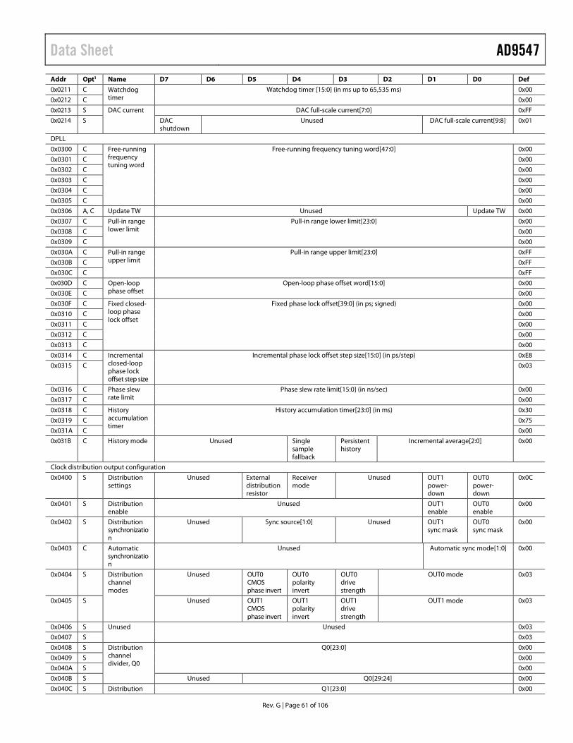
Data Sheet AD9547 Addr Opt1 Name D7 D6 D5 D4 D3 D2 D1 D0 Def
0x0211 C Watchdog timer
Watchdog timer [15:0] (in ms up to 65,535 ms) 0x00
0x0212 C 0x00
0x0213 S DAC current DAC full-scale current[7:0] 0xFF
0x0214 S DAC shutdown
Unused DAC full-scale current[9:8] 0x01
DPLL
0x0300 C Free-running frequency tuning word
Free-running frequency tuning word[47:0] 0x00
0x0301 C 0x00
0x0302 C 0x00
0x0303 C 0x00
0x0304 C 0x00
0x0305 C 0x00
0x0306 A, C Update TW Unused Update TW 0x00
0x0307 C Pull-in range lower limit
Pull-in range lower limit[23:0] 0x00
0x0308 C 0x00
0x0309 C 0x00
0x030A C Pull-in range upper limit
Pull-in range upper limit[23:0] 0xFF
0x030B C 0xFF
0x030C C 0xFF
0x030D C Open-loop phase offset
Open-loop phase offset word[15:0] 0x00
0x030E C 0x00
0x030F C Fixed closed-loop phase lock offset
Fixed phase lock offset[39:0] (in ps; signed) 0x00
0x0310 C 0x00
0x0311 C 0x00
0x0312 C 0x00
0x0313 C 0x00
0x0314 C Incremental closed-loop phase lock offset step size
Incremental phase lock offset step size[15:0] (in ps/step) 0xE8
0x0315 C 0x03
0x0316 C Phase slew rate limit
Phase slew rate limit[15:0] (in ns/sec) 0x00
0x0317 C 0x00
0x0318 C History accumulation timer
History accumulation timer[23:0] (in ms) 0x30
0x0319 C 0x75
0x031A C 0x00
0x031B C History mode Unused Single sample fallback
Persistent history
Incremental average[2:0] 0x00
Clock distribution output configuration
0x0400 S Distribution settings
Unused External distribution resistor
Receiver mode
Unused OUT1 power-down
OUT0 power-down
0x0C
0x0401 S Distribution enable
Unused OUT1 enable
OUT0 enable
0x00
0x0402 S Distribution synchronization
Unused Sync source[1:0] Unused OUT1 sync mask
OUT0 sync mask
0x00
0x0403 C Automatic synchronization
Unused Automatic sync mode[1:0] 0x00
0x0404 S Distribution channel modes
Unused OUT0 CMOS phase invert
OUT0 polarity invert
OUT0 drive strength
OUT0 mode 0x03
0x0405 S Unused OUT1 CMOS phase invert
OUT1 polarity invert
OUT1 drive strength
OUT1 mode 0x03
0x0406 S Unused Unused 0x03
0x0407 S 0x03
0x0408 S Distribution channel divider, Q0
Q0[23:0] 0x00
0x0409 S 0x00
0x040A S 0x00
0x040B S Unused Q0[29:24] 0x00
0x040C S Distribution Q1[23:0] 0x00
Rev. G | Page 61 of 106
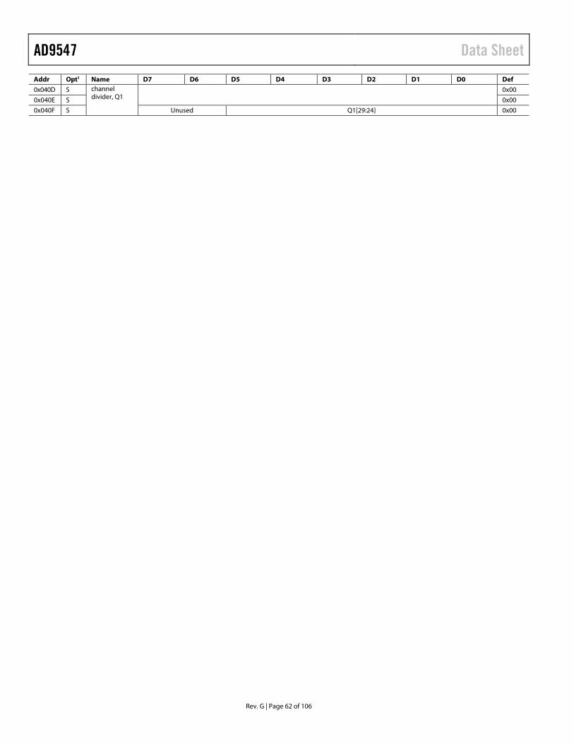
AD9547 Data Sheet Addr Opt1 Name D7 D6 D5 D4 D3 D2 D1 D0 Def
0x040D S channel divider, Q1
0x00
0x040E S 0x00
0x040F S Unused Q1[29:24] 0x00
Rev. G | Page 62 of 106
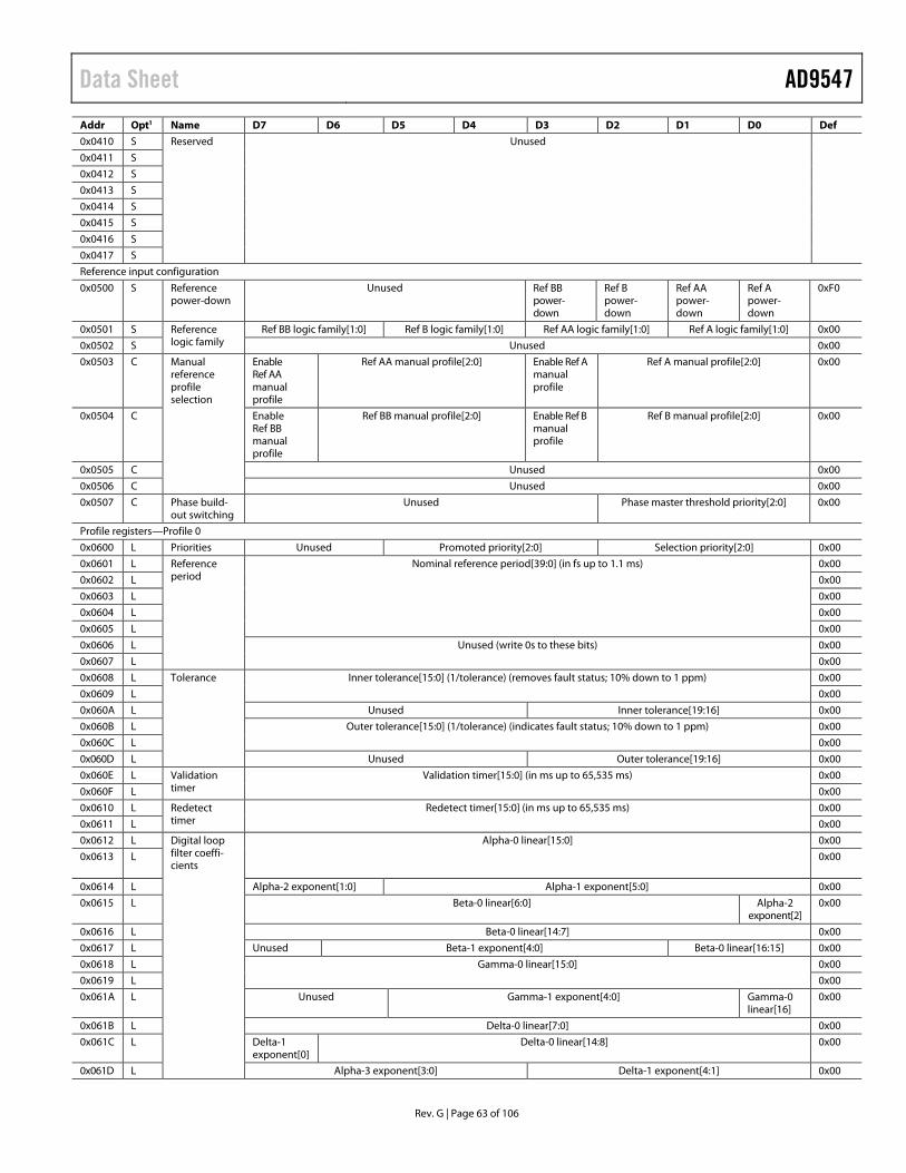
Data Sheet AD9547 Addr Opt1 Name D7 D6 D5 D4 D3 D2 D1 D0 Def
0x0410 S Reserved Unused
0x0411 S
0x0412 S
0x0413 S
0x0414 S
0x0415 S
0x0416 S
0x0417 S
Reference input configuration
0x0500 S Reference power-down
Unused Ref BB power-down
Ref B power-down
Ref AA power-down
Ref A power-down
0xF0
0x0501 S Reference logic family
Ref BB logic family[1:0] Ref B logic family[1:0] Ref AA logic family[1:0] Ref A logic family[1:0] 0x00
0x0502 S Unused 0x00
0x0503 C Manual reference profile selection
Enable Ref AA manual profile
Ref AA manual profile[2:0] Enable Ref A manual profile
Ref A manual profile[2:0] 0x00
0x0504 C Enable Ref BB manual profile
Ref BB manual profile[2:0] Enable Ref B manual profile
Ref B manual profile[2:0] 0x00
0x0505 C Unused 0x00
0x0506 C Unused 0x00
0x0507 C Phase build-out switching
Unused Phase master threshold priority[2:0] 0x00
Profile registers—Profile 0
0x0600 L Priorities Unused Promoted priority[2:0] Selection priority[2:0] 0x00
0x0601 L Reference period
Nominal reference period[39:0] (in fs up to 1.1 ms) 0x00
0x0602 L 0x00
0x0603 L 0x00
0x0604 L 0x00
0x0605 L 0x00
0x0606 L Unused (write 0s to these bits) 0x00
0x0607 L 0x00
0x0608 L Tolerance Inner tolerance[15:0] (1/tolerance) (removes fault status; 10% down to 1 ppm) 0x00
0x0609 L 0x00
0x060A L Unused Inner tolerance[19:16] 0x00
0x060B L Outer tolerance[15:0] (1/tolerance) (indicates fault status; 10% down to 1 ppm) 0x00
0x060C L 0x00
0x060D L Unused Outer tolerance[19:16] 0x00
0x060E L Validation timer
Validation timer[15:0] (in ms up to 65,535 ms) 0x00
0x060F L 0x00
0x0610 L Redetect timer
Redetect timer[15:0] (in ms up to 65,535 ms) 0x00
0x0611 L 0x00
0x0612 L Digital loop filter coeffi-cients
Alpha-0 linear[15:0] 0x00
0x0613 L 0x00
0x0614 L Alpha-2 exponent[1:0] Alpha-1 exponent[5:0] 0x00
0x0615 L Beta-0 linear[6:0] Alpha-2 exponent[2]
0x00
0x0616 L Beta-0 linear[14:7] 0x00
0x0617 L Unused Beta-1 exponent[4:0] Beta-0 linear[16:15] 0x00
0x0618 L Gamma-0 linear[15:0] 0x00
0x0619 L 0x00
0x061A L Unused Gamma-1 exponent[4:0] Gamma-0 linear[16]
0x00
0x061B L Delta-0 linear[7:0] 0x00
0x061C L Delta-1 exponent[0]
Delta-0 linear[14:8] 0x00
0x061D L Alpha-3 exponent[3:0] Delta-1 exponent[4:1] 0x00
Rev. G | Page 63 of 106
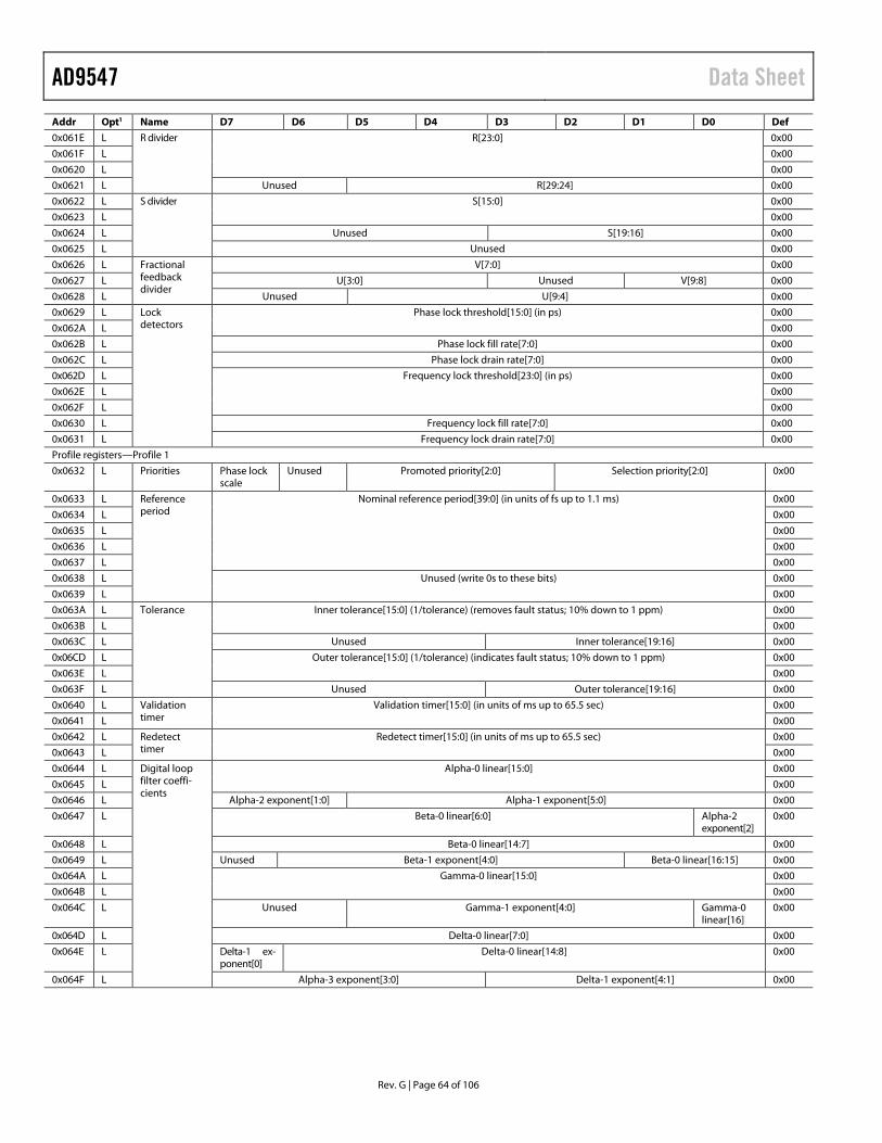
AD9547 Data Sheet Addr Opt1 Name D7 D6 D5 D4 D3 D2 D1 D0 Def
0x061E L R divider R[23:0] 0x00
0x061F L 0x00
0x0620 L 0x00
0x0621 L Unused R[29:24] 0x00
0x0622 L S divider S[15:0] 0x00
0x0623 L 0x00
0x0624 L Unused S[19:16] 0x00
0x0625 L Unused 0x00
0x0626 L Fractional feedback divider
V[7:0] 0x00
0x0627 L U[3:0] Unused V[9:8] 0x00
0x0628 L Unused U[9:4] 0x00
0x0629 L Lock detectors
Phase lock threshold[15:0] (in ps) 0x00
0x062A L 0x00
0x062B L Phase lock fill rate[7:0] 0x00
0x062C L Phase lock drain rate[7:0] 0x00
0x062D L Frequency lock threshold[23:0] (in ps) 0x00
0x062E L 0x00
0x062F L 0x00
0x0630 L Frequency lock fill rate[7:0] 0x00
0x0631 L Frequency lock drain rate[7:0] 0x00
Profile registers—Profile 1
0x0632 L Priorities Phase lock scale
Unused Promoted priority[2:0] Selection priority[2:0] 0x00
0x0633 L Reference period
Nominal reference period[39:0] (in units of fs up to 1.1 ms) 0x00
0x0634 L 0x00
0x0635 L 0x00
0x0636 L 0x00
0x0637 L 0x00
0x0638 L Unused (write 0s to these bits) 0x00
0x0639 L 0x00
0x063A L Tolerance Inner tolerance[15:0] (1/tolerance) (removes fault status; 10% down to 1 ppm) 0x00
0x063B L 0x00
0x063C L Unused Inner tolerance[19:16] 0x00
0x06CD L Outer tolerance[15:0] (1/tolerance) (indicates fault status; 10% down to 1 ppm) 0x00
0x063E L 0x00
0x063F L Unused Outer tolerance[19:16] 0x00
0x0640 L Validation timer
Validation timer[15:0] (in units of ms up to 65.5 sec) 0x00
0x0641 L 0x00
0x0642 L Redetect timer
Redetect timer[15:0] (in units of ms up to 65.5 sec) 0x00
0x0643 L 0x00
0x0644 L Digital loop filter coeffi-cients
Alpha-0 linear[15:0] 0x00
0x0645 L 0x00
0x0646 L Alpha-2 exponent[1:0] Alpha-1 exponent[5:0] 0x00
0x0647 L Beta-0 linear[6:0] Alpha-2 exponent[2]
0x00
0x0648 L Beta-0 linear[14:7] 0x00
0x0649 L Unused Beta-1 exponent[4:0] Beta-0 linear[16:15] 0x00
0x064A L Gamma-0 linear[15:0] 0x00
0x064B L 0x00
0x064C L Unused Gamma-1 exponent[4:0] Gamma-0 linear[16]
0x00
0x064D L Delta-0 linear[7:0] 0x00
0x064E L Delta-1 ex-ponent[0]
Delta-0 linear[14:8] 0x00
0x064F L Alpha-3 exponent[3:0] Delta-1 exponent[4:1] 0x00
Rev. G | Page 64 of 106
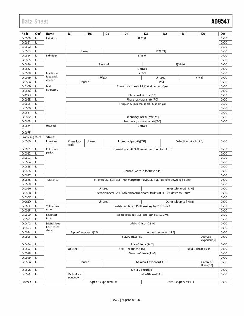
Data Sheet AD9547 Addr Opt1 Name D7 D6 D5 D4 D3 D2 D1 D0 Def
0x0650 L R divider R[23:0] 0x00
0x0651 L 0x00
0x0652 L 0x00
0x0653 L Unused R[29:24] 0x00
0x0654 L S divider S[15:0] 0x00
0x0655 L 0x00
0x0656 L Unused S[19:16] 0x00
0x0657 L Unused 0x00
0x0658 L Fractional feedback divider
V[7:0] 0x00
0x0659 L U[3:0] Unused V[9:8] 0x00
0x065A L Unused U[9:4] 0x00
0x065B L Lock detectors
Phase lock threshold[15:0] (in units of ps) 0x00
0x065C L 0x00
0x065D L Phase lock fill rate[7:0] 0x00
0x065E L Phase lock drain rate[7:0] 0x00
0x065F L Frequency lock threshold[23:0] (in ps) 0x00
0x0660 L 0x00
0x0661 L 0x00
0x0662 L Frequency lock fill rate[7:0] 0x00
0x0663 L Frequency lock drain rate[7:0] 0x00
0x0664 to 0x067F
Unused Unused
Profile registers—Profile 2
0x0680 L Priorities Phase lock scale
Unused Promoted priority[2:0] Selection priority[2:0] 0x00
0x0681 L Reference period
Nominal period[39:0] (in units of fs up to 1.1 ms) 0x00
0x0682 L 0x00
0x0683 L 0x00
0x0684 L 0x00
0x0685 L 0x00
0x0686 L Unused (write 0s to these bits) 0x00
0x0687 L 0x00
0x0688 L Tolerance Inner tolerance[15:0] (1/tolerance) (removes fault status; 10% down to 1 ppm) 0x00
0x0689 L 0x00
0x068A L Unused Inner tolerance[19:16] 0x00
0x068B L Outer tolerance[15:0] (1/tolerance) (indicates fault status; 10% down to 1 ppm) 0x00
0x068C L 0x00
0x068D L Unused Outer tolerance [19:16] 0x00
0x068E L Validation timer
Validation timer[15:0] (ms) (up to 65,535 ms) 0x00
0x068F L 0x00
0x0690 L Redetect timer
Redetect timer[15:0] (ms) (up to 65,535 ms) 0x00
0x0691 L 0x00
0x0692 L Digital loop filter coeffi-cients
Alpha-0 linear[15:0] 0x00
0x0693 L 0x00
0x0694 L Alpha-2 exponent[1:0] Alpha-1 exponent[5:0] 0x00
0x0695 L Beta-0 linear[6:0] Alpha-2 exponent[2]
0x00
0x0696 L Beta-0 linear[14:7] 0x00
0x0697 L Unused Beta-1 exponent[4:0] Beta-0 linear[16:15] 0x00
0x0698 L Gamma-0 linear[15:0] 0x00
0x0699 L 0x00
0x069A L Unused Gamma-1 exponent[4:0] Gamma-0 linear[16]
0x00
0x069B L Delta-0 linear[7:0] 0x00
0x069C L Delta-1 ex-ponent[0]
Delta-0 linear[14:8] 0x00
0x069D L Alpha-3 exponent[3:0] Delta-1 exponent[4:1] 0x00
Rev. G | Page 65 of 106
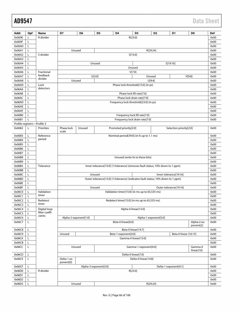
AD9547 Data Sheet Addr Opt1 Name D7 D6 D5 D4 D3 D2 D1 D0 Def
0x069E L R divider R[23:0] 0x00
0x069F L 0x00
0x06A0 L 0x00
0x06A1 L Unused R[29:24] 0x00
0x06A2 L S divider S[15:0] 0x00
0x06A3 L 0x00
0x06A4 L Unused S[19:16] 0x00
0x06A5 L Unused 0x00
0x06A6 L Fractional feedback divider
V[7:0] 0x00
0x06A7 L U[3:0] Unused V[9:8] 0x00
0x06A8 L Unused U[9:4] 0x00
0x06A9 L Lock detectors
Phase lock threshold[15:0] (in ps) 0x00
0x06AA L 0x00
0x06AB L Phase lock fill rate[7:0] 0x00
0x06AC L Phase lock drain rate[7:0] 0x00
0x06AD L Frequency lock threshold[23:0] (in ps) 0x00
0x06AE L 0x00
0x06AF L 0x00
0x06B0 L Frequency lock fill rate[7:0] 0x00
0x06B1 L Frequency lock drain rate[7:0] 0x00
Profile registers—Profile 3
0x06B2 L Priorities Phase lock scale
Unused Promoted priority[2:0] Selection priority[2:0] 0x00
0x06B3 L Reference period
Nominal period[39:0] (in fs up to 1.1 ms) 0x00
0x06B4 L 0x00
0x06B5 L 0x00
0x06B6 L 0x00
0x06B7 L 0x00
0x06B8 L Unused (write 0s to these bits) 0x00
0x06B9 L 0x00
0x06BA L Tolerance Inner tolerance[15:0] (1/tolerance) (removes fault status; 10% down to 1 ppm) 0x00
0x06BB L 0x00
0x06BC L Unused Inner tolerance[19:16] 0x00
0x06BD L Outer tolerance[15:0] (1/tolerance) (indicates fault status; 10% down to 1 ppm) 0x00
0x06BE L 0x00
0x06BF L Unused Outer tolerance[19:16] 0x00
0x06C0 L Validation timer
Validation timer[15:0] (in ms up to 65,535 ms) 0x00
0x06C1 L 0x00
0x06C2 L Redetect timer
Redetect timer[15:0] (in ms up to 65,535 ms) 0x00
0x06C3 L 0x00
0x06C4 L Digital loop filter coeffi-cients
Alpha-0 linear[15:0] 0x00
0x06C5 L 0x00
0x06C6 L Alpha-2 exponent[1:0] Alpha-1 exponent[5:0] 0x00
0x06C7 L Beta-0 linear[6:0] Alpha-2 ex-ponent[2]
0x00
0x06C8 L Beta-0 linear[14:7] 0x00
0x06C9 L Unused Beta-1 exponent[4:0] Beta-0 linear [16:15] 0x00
0x06CA L Gamma-0 linear[15:0] 0x00
0x06CB L 0x00
0x06CC L Unused Gamma-1 exponent[4:0] Gamma-0 linear[16]
0x00
0x06CD L Delta-0 linear[7:0] 0x00
0x06CE L Delta-1 ex- ponent[0]
Delta-0 linear[14:8] 0x00
0x06CF L Alpha-3 exponent[3:0] Delta-1 exponent[4:1] 0x00
0x06D0 L R divider R[23:0] 0x00
0x06D1 L 0x00
0x06D2 L 0x00
0x06D3 L Unused R[29:24] 0x00
Rev. G | Page 66 of 106
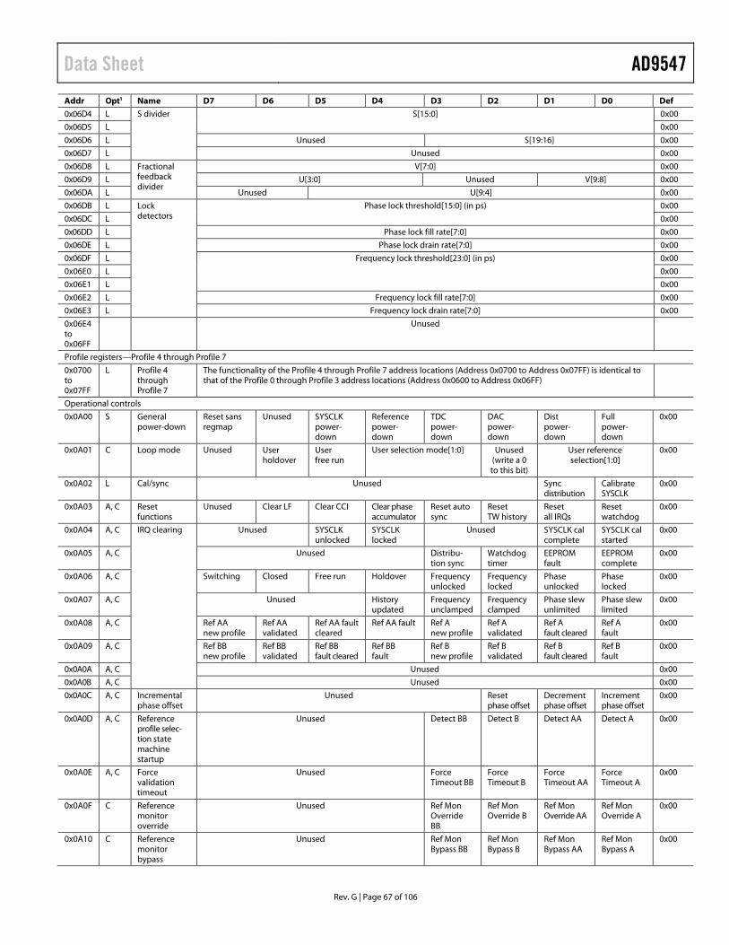
Data Sheet AD9547 Addr Opt1 Name D7 D6 D5 D4 D3 D2 D1 D0 Def
0x06D4 L S divider S[15:0] 0x00
0x06D5 L 0x00
0x06D6 L Unused S[19:16] 0x00
0x06D7 L Unused 0x00
0x06D8 L Fractional feedback divider
V[7:0] 0x00
0x06D9 L U[3:0] Unused V[9:8] 0x00
0x06DA L Unused U[9:4] 0x00
0x06DB L Lock detectors
Phase lock threshold[15:0] (in ps) 0x00
0x06DC L 0x00
0x06DD L Phase lock fill rate[7:0] 0x00
0x06DE L Phase lock drain rate[7:0] 0x00
0x06DF L Frequency lock threshold[23:0] (in ps) 0x00
0x06E0 L 0x00
0x06E1 L 0x00
0x06E2 L Frequency lock fill rate[7:0] 0x00
0x06E3 L Frequency lock drain rate[7:0] 0x00
0x06E4 to 0x06FF
Unused
Profile registers—Profile 4 through Profile 7
0x0700 to 0x07FF
L Profile 4 through Profile 7
The functionality of the Profile 4 through Profile 7 address locations (Address 0x0700 to Address 0x07FF) is identical to that of the Profile 0 through Profile 3 address locations (Address 0x0600 to Address 0x06FF)
Operational controls
0x0A00 S General power-down
Reset sans regmap
Unused SYSCLK power-down
Reference power-down
TDC power-down
DAC power-down
Dist power-down
Full power-down
0x00
0x0A01 C Loop mode Unused User holdover
User free run
User selection mode[1:0] Unused (write a 0 to this bit)
User reference selection[1:0]
0x00
0x0A02 L Cal/sync Unused Sync distribution
Calibrate SYSCLK
0x00
0x0A03 A, C Reset functions
Unused Clear LF Clear CCI Clear phase accumulator
Reset auto sync
Reset TW history
Reset all IRQs
Reset watchdog
0x00
0x0A04 A, C IRQ clearing Unused SYSCLK unlocked
SYSCLK locked
Unused SYSCLK cal complete
SYSCLK cal started
0x00
0x0A05 A, C Unused Distribu-tion sync
Watchdog timer
EEPROM fault
EEPROM complete
0x00
0x0A06 A, C Switching Closed Free run Holdover Frequency unlocked
Frequency locked
Phase unlocked
Phase locked
0x00
0x0A07 A, C Unused History updated
Frequency unclamped
Frequency clamped
Phase slew unlimited
Phase slew limited
0x00
0x0A08 A, C Ref AA new profile
Ref AA validated
Ref AA fault cleared
Ref AA fault Ref A new profile
Ref A validated
Ref A fault cleared
Ref A fault
0x00
0x0A09 A, C Ref BB new profile
Ref BB validated
Ref BB fault cleared
Ref BB fault
Ref B new profile
Ref B validated
Ref B fault cleared
Ref B fault
0x00
0x0A0A A, C Unused 0x00
0x0A0B A, C Unused 0x00
0x0A0C A, C Incremental phase offset
Unused Reset phase offset
Decrement phase offset
Increment phase offset
0x00
0x0A0D A, C Reference profile selec-tion state machine startup
Unused Detect BB Detect B Detect AA Detect A 0x00
0x0A0E A, C Force validation timeout
Unused Force Timeout BB
Force Timeout B
Force Timeout AA
Force Timeout A
0x00
0x0A0F C Reference monitor override
Unused Ref Mon Override BB
Ref Mon Override B
Ref Mon Override AA
Ref Mon Override A
0x00
0x0A10 C Reference monitor bypass
Unused Ref Mon Bypass BB
Ref Mon Bypass B
Ref Mon Bypass AA
Ref Mon Bypass A
0x00
Rev. G | Page 67 of 106
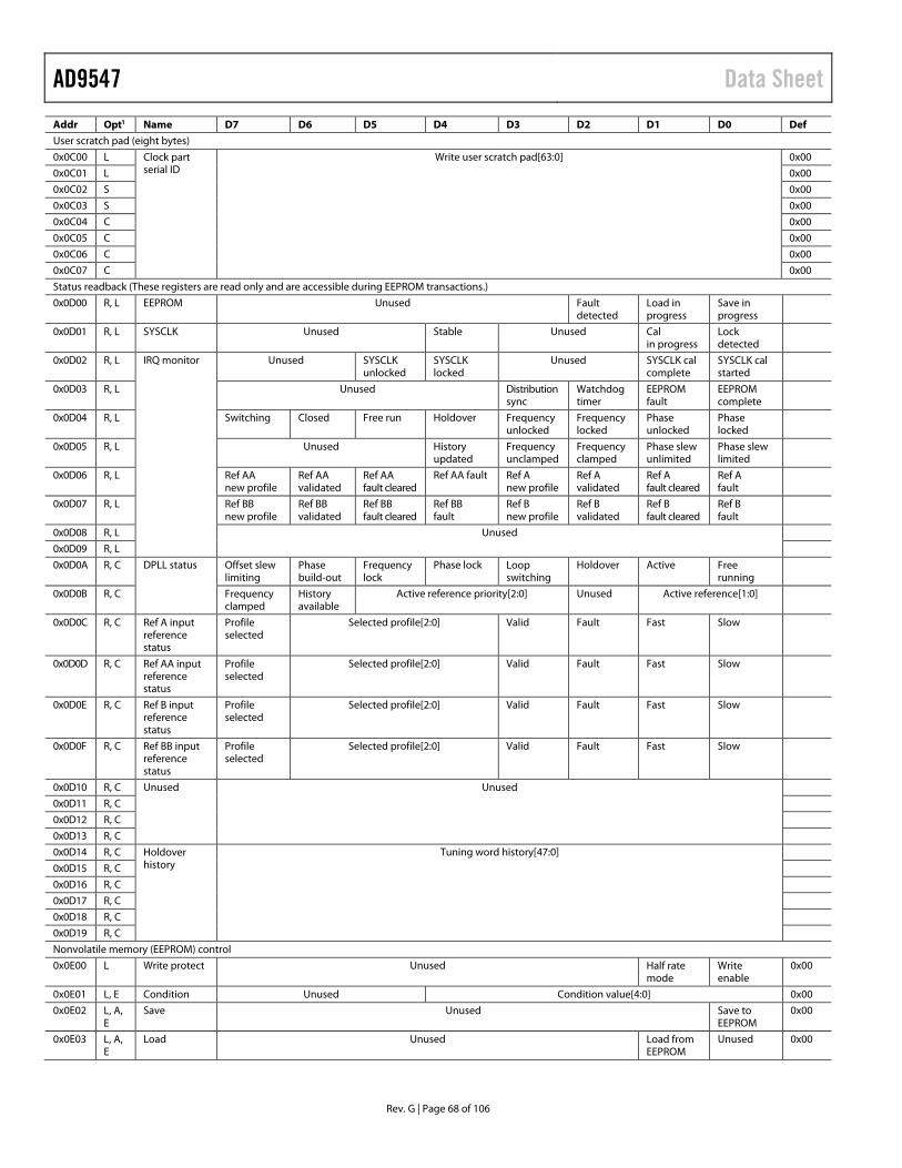
AD9547 Data Sheet Addr Opt1 Name D7 D6 D5 D4 D3 D2 D1 D0 Def
User scratch pad (eight bytes)
0x0C00 L Clock part serial ID
Write user scratch pad[63:0]
0x00
0x0C01 L 0x00
0x0C02 S 0x00
0x0C03 S 0x00
0x0C04 C 0x00
0x0C05 C 0x00
0x0C06 C 0x00
0x0C07 C 0x00
Status readback (These registers are read only and are accessible during EEPROM transactions.)
0x0D00 R, L EEPROM Unused Fault detected
Load in progress
Save in progress
0x0D01 R, L SYSCLK Unused Stable Unused Cal in progress
Lock detected
0x0D02 R, L IRQ monitor Unused SYSCLK unlocked
SYSCLK locked
Unused SYSCLK cal complete
SYSCLK cal started
0x0D03 R, L Unused Distribution sync
Watchdog timer
EEPROM fault
EEPROM complete
0x0D04 R, L Switching Closed Free run Holdover Frequency unlocked
Frequency locked
Phase unlocked
Phase locked
0x0D05 R, L Unused History updated
Frequency unclamped
Frequency clamped
Phase slew unlimited
Phase slew limited
0x0D06 R, L Ref AA new profile
Ref AA validated
Ref AA fault cleared
Ref AA fault Ref A new profile
Ref A validated
Ref A fault cleared
Ref A fault
0x0D07 R, L Ref BB new profile
Ref BB validated
Ref BB fault cleared
Ref BB fault
Ref B new profile
Ref B validated
Ref B fault cleared
Ref B fault
0x0D08 R, L Unused
0x0D09 R, L
0x0D0A R, C DPLL status Offset slew limiting
Phase build-out
Frequency lock
Phase lock Loop switching
Holdover Active Free running
0x0D0B R, C Frequency clamped
History available
Active reference priority[2:0] Unused Active reference[1:0]
0x0D0C R, C Ref A input reference status
Profile selected
Selected profile[2:0] Valid Fault Fast Slow
0x0D0D R, C Ref AA input reference status
Profile selected
Selected profile[2:0] Valid Fault Fast Slow
0x0D0E R, C Ref B input reference status
Profile selected
Selected profile[2:0] Valid Fault Fast Slow
0x0D0F R, C Ref BB input reference status
Profile selected
Selected profile[2:0] Valid Fault Fast Slow
0x0D10 R, C Unused Unused
0x0D11 R, C
0x0D12 R, C
0x0D13 R, C
0x0D14 R, C Holdover history
Tuning word history[47:0]
0x0D15 R, C
0x0D16 R, C
0x0D17 R, C
0x0D18 R, C
0x0D19 R, C
Nonvolatile memory (EEPROM) control
0x0E00 L Write protect Unused Half rate mode
Write enable
0x00
0x0E01 L, E Condition Unused Condition value[4:0] 0x00
0x0E02 L, A, E
Save Unused Save to EEPROM
0x00
0x0E03 L, A, E
Load Unused Load from EEPROM
Unused 0x00
Rev. G | Page 68 of 106
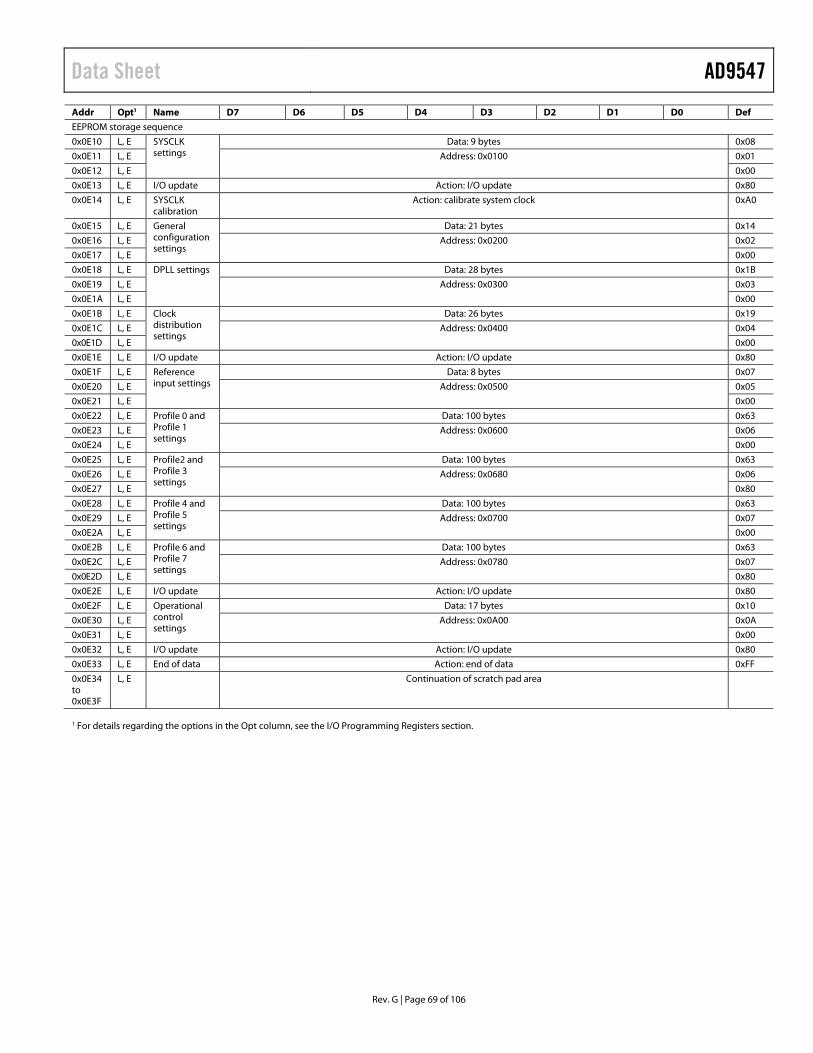
Data Sheet AD9547 Addr Opt1 Name D7 D6 D5 D4 D3 D2 D1 D0 Def
EEPROM storage sequence
0x0E10 L, E SYSCLK settings
Data: 9 bytes 0x08
0x0E11 L, E Address: 0x0100 0x01
0x0E12 L, E 0x00
0x0E13 L, E I/O update Action: I/O update 0x80
0x0E14 L, E SYSCLK calibration
Action: calibrate system clock 0xA0
0x0E15 L, E General configuration settings
Data: 21 bytes 0x14
0x0E16 L, E Address: 0x0200 0x02
0x0E17 L, E 0x00
0x0E18 L, E DPLL settings Data: 28 bytes 0x1B
0x0E19 L, E Address: 0x0300 0x03
0x0E1A L, E 0x00
0x0E1B L, E Clock distribution settings
Data: 26 bytes 0x19
0x0E1C L, E Address: 0x0400 0x04
0x0E1D L, E 0x00
0x0E1E L, E I/O update Action: I/O update 0x80
0x0E1F L, E Reference input settings
Data: 8 bytes 0x07
0x0E20 L, E Address: 0x0500 0x05
0x0E21 L, E 0x00
0x0E22 L, E Profile 0 and Profile 1 settings
Data: 100 bytes 0x63
0x0E23 L, E Address: 0x0600 0x06
0x0E24 L, E 0x00
0x0E25 L, E Profile2 and Profile 3 settings
Data: 100 bytes 0x63
0x0E26 L, E Address: 0x0680 0x06
0x0E27 L, E 0x80
0x0E28 L, E Profile 4 and Profile 5 settings
Data: 100 bytes 0x63
0x0E29 L, E Address: 0x0700 0x07
0x0E2A L, E 0x00
0x0E2B L, E Profile 6 and Profile 7 settings
Data: 100 bytes 0x63
0x0E2C L, E Address: 0x0780 0x07
0x0E2D L, E 0x80
0x0E2E L, E I/O update Action: I/O update 0x80
0x0E2F L, E Operational control settings
Data: 17 bytes 0x10
0x0E30 L, E Address: 0x0A00 0x0A
0x0E31 L, E 0x00
0x0E32 L, E I/O update Action: I/O update 0x80
0x0E33 L, E End of data Action: end of data 0xFF
0x0E34 to 0x0E3F
L, E Continuation of scratch pad area
1 For details regarding the options in the Opt column, see the I/O Programming Registers section.
Rev. G | Page 69 of 106

AD9547 Data Sheet
REGISTER BIT DESCRIPTIONS SERIAL PORT CONFIGURATION AND PART IDENTIFICATION (REGISTER 0x0000 TO REGISTER 0x0005)
Table 38. SPI Control/I2C Control Address Bit Bit Name Description 0x0000 7 Unidirectional Select SPI port SDO pin operating mode.
0 (default) = 3-wire. 1 = 4-wire (SDO pin enabled).
6 LSB first/IncAddr Bit order for SPI port. 0 (default) = most significant bit and byte first (multibyte transfers use incrementing address). 1 = least significant bit and byte first (multibyte transfers use decrementing address).
5 Soft reset Device reset (invokes an EEPROM download if M[7:3] ≠ 0). 0 (default) = normal operation. 1 = reset.
4 Long instruction 16-bit mode (the only mode supported by the device). This bit is read only and reads back as Logic 1.
[3:0] Unused Unused.
Table 39. Reserved Register Address Bit Bit Name Description 0x0001 [7:0] Unused Unused.
Table 40. Silicon Revision Level (Read Only) Address Bit Bit Name Description 0x0002 [7:0] Silicon revision number Default = 0xF6 = 0b11110110.
Table 41. Device ID (Read Only) Address Bit Bit Name Description 0x0003 [7:0] Device ID Default = 0x48 = 0b01001000.
Table 42. Register Readback Control Address Bit Bit Name Description 0x0004 [7:1] Unused Unused.
0 Read buffered register For buffered registers, serial port readback reads from actual (active) registers instead of from the buffer. 0 (default) = reads values currently applied to the device’s internal logic. 1 = reads buffered values that take effect on the next assertion of the I/O update.
Table 43. Soft I/O Update Address Bit Bit Name Description 0x0005 [7:1] Unused Unused.
0 I/O update Writing a 1 to this bit transfers the data in the serial I/O buffer registers to the device’s internal control registers. This is an autoclearing bit.
Rev. G | Page 70 of 106

Data Sheet AD9547
SYSTEM CLOCK (SYSCLK) (REGISTER 0x0100 TO REGISTER 0x0108)
Table 44. Charge Pump and Lock Detect Control Address Bit Bit Name Description 0x0100 7 External loop filter enable Enables use of an external SYSCLK PLL loop filter.
0 (default) = internal loop filter. 1 = external loop filter.
6 Charge pump mode Charge pump current control. 0 (default) = automatic. 1 = manual.
[5:3] Charge pump current Selects charge pump current when Bit 6 = 1. 000 = 125 µA. 001 = 250 µA. 010 = 375 µA. 011 (default) = 500 µA. 100 = 625 µA. 101 = 750 µA. 110 = 875 µA. 111 = 1000 µA.
2 Lock detect timer disable Enable the SYSCLK PLL lock detect timer. 0 (default) = enable. 1 = disable.
[1:0] Lock detect timer Select lock detect timer depth. 00 (default) = 128. 01 = 256. 10 = 512. 11 = 1024.
Table 45. N Divider Address Bit Bit Name Description 0x0101 [7:0] N divider System clock PLL feedback divider value: 6 ≤ N ≤ 255 (default = 0x28 = 40).
Table 46. System Clock Input Options Address Bit Bit Name Description 0x0102 7 Unused Unused.
6 M divider reset Reset the M divider. 0 = normal operation. 1 (default) = reset. When not using the M divider, program this bit to Logic 1.
[5:4] M divider System clock input divider. 00 (default) = 1. 01 = 2. 10 = 4. 11 = 8.
3 2× frequency multiplier enable
Enable the 2× frequency multiplier. 0 (default) = disable. 1 = enable.
2 PLL enable Enable the SYSCLK PLL. 0 = disable. 1 (default) = enable.
[1:0] SYSCLK source Input mode select for SYSCLKx pins. 00 = crystal resonator. 01 (default) = low frequency clock source. 10 = high frequency (direct) clock source. 11 = input receiver power-down.
Rev. G | Page 71 of 106

AD9547 Data Sheet
Table 47. Nominal System Clock (SYSCLK) Period1 Address Bit Bit Name Description 0x0103 [7:0] Nominal SYSCLK period
(expressed in fs) System clock period, Bits[7:0].
0x0104 [7:0] System clock period, Bits[15:8]. 0x0105 [7:5] Unused Unused.
[4:0] Nominal SYSCLK period System clock period, Bits[20:16].
1 Units are femtoseconds (fs). The default value is 0x0F424 = 1,000,000 (1 ns) and implies a system clock frequency of 1 GHz.
Table 48. System Clock Stability Period1 Address Bit Bit Name Description 0x0106 [7:0] SYSCLK stability period
(expressed in ms) System clock stability period, Bits[7:0] (default = 0x01).
0x0107 [7:0] System clock stability period, Bits[15:8] (default = 0x00). 0x0108 [7:4] Unused Unused.
[3:0] SYSCLK stability period System clock stability period, Bits[19:16] (default = 0x0) (default period = 0x00001, or 1 ms).
1 Units are milliseconds (ms). The default value is 0x00001 = 1 (1 ms).
GENERAL CONFIGURATION (REGISTER 0x0200 TO REGISTER 0x0214) Register 0x0200 to Register 0x0207—Multifunction Pin Control (M0 to M7)
Table 49. Multifunction Pin (M0 to M7) Control1 Address Bit Bit Name Description 0x0200 7 M0 in/out In/out control for the M0 pin.
0 (default) = input (control pin). 1 = output (status pin).
[6:0] M0 function See Table 25 and Table 26 (default = 0xb0000000). 0x0201 7 M1 in/out In/out control for the M1 pin (same as M0).
[6:0] M1 function See Table 25 and Table 26 (default = 0xb0000000). 0x0202 7 M2 in/out In/out control for the M2 pin (same as M0).
[6:0] M2 function See Table 25 and Table 26 (default = 0xb0000000). 0x0203 7 M3 in/out In/out control for the M3 pin (same as M0).
[6:0] M3 function See Table 25 and Table 26 (default = 0xb0000000). 0x0204 7 M4 in/out In/out control for the M4 pin (same as M0).
[6:0] M4 function See Table 25 and Table 26 (default = 0xb0000000). 0x0205 7 M5 in/out In/out control for the M5 pin (same as M0).
[6:0] M5 function See Table 25 and Table 26 (default = 0xb0000000). 0x0206 7 M6 in/out In/out control for the M6 pin (same as M0).
[6:0] M6 function See Table 25 and Table 26 (default = 0xb0000000). 0x0207 7 M7 in/out In/out control for the M7 pin (same as M0).
[6:0] M7 function See Table 25 and Table 26 (default = 0xb0000000).
1 The default setting for all the multifunction pins is as an unused control input pin.
Table 50. IRQ Pin Output Mode Address Bit Bit Name Description 0x0208 [7:2] Unused Unused.
[1:0] IRQ pin output mode Select the output mode of the IRQ pin. 00 (default) = NMOS, open drain (requires an external pull-up resistor). 01 = PMOS, open drain (requires an external pull-down resistor). 10 = CMOS, active high. 11 = CMOS, active low.
Rev. G | Page 72 of 106
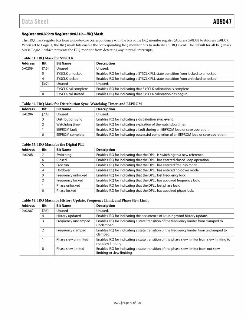
Data Sheet AD9547 Register 0x0209 to Register 0x0210—IRQ Mask
The IRQ mask register bits form a one-to-one correspondence with the bits of the IRQ monitor register (Address 0x0D02 to Address 0x0D09). When set to Logic 1, the IRQ mask bits enable the corresponding IRQ monitor bits to indicate an IRQ event. The default for all IRQ mask bits is Logic 0, which prevents the IRQ monitor from detecting any internal interrupts.
Table 51. IRQ Mask for SYSCLK Address Bit Bit Name Description 0x0209 [7:6] Unused Unused.
5 SYSCLK unlocked Enables IRQ for indicating a SYSCLK PLL state transition from locked to unlocked. 4 SYSCLK locked Enables IRQ for indicating a SYSCLK PLL state transition from unlocked to locked. [3:2] Unused Unused. 1 SYSCLK cal complete Enables IRQ for indicating that SYSCLK calibration is complete. 0 SYSCLK cal started Enables IRQ for indicating that SYSCLK calibration has begun.
Table 52. IRQ Mask for Distribution Sync, Watchdog Timer, and EEPROM Address Bit Bit Name Description 0x020A [7:4] Unused Unused.
3 Distribution sync Enables IRQ for indicating a distribution sync event. 2 Watchdog timer Enables IRQ for indicating expiration of the watchdog timer. 1 EEPROM fault Enables IRQ for indicating a fault during an EEPROM load or save operation. 0 EEPROM complete Enables IRQ for indicating successful completion of an EEPROM load or save operation.
Table 53. IRQ Mask for the Digital PLL Address Bit Bit Name Description 0x020B 7 Switching Enables IRQ for indicating that the DPLL is switching to a new reference.
6 Closed Enables IRQ for indicating that the DPLL has entered closed-loop operation. 5 Free run Enables IRQ for indicating that the DPLL has entered free-run mode. 4 Holdover Enables IRQ for indicating that the DPLL has entered holdover mode. 3 Frequency unlocked Enables IRQ for indicating that the DPLL lost frequency lock. 2 Frequency locked Enables IRQ for indicating that the DPLL has acquired frequency lock. 1 Phase unlocked Enables IRQ for indicating that the DPLL lost phase lock. 0 Phase locked Enables IRQ for indicating that the DPLL has acquired phase lock.
Table 54. IRQ Mask for History Update, Frequency Limit, and Phase Slew Limit Address Bit Bit Name Description 0x020C [7:5] Unused Unused.
4 History updated Enables IRQ for indicating the occurrence of a tuning word history update. 3 Frequency unclamped Enables IRQ for indicating a state transition of the frequency limiter from clamped to
unclamped. 2 Frequency clamped Enables IRQ for indicating a state transition of the frequency limiter from unclamped to
clamped. 1 Phase slew unlimited Enables IRQ for indicating a state transition of the phase slew limiter from slew limiting to
not slew limiting. 0 Phase slew limited Enables IRQ for indicating a state transition of the phase slew limiter from not slew
limiting to slew limiting.
Rev. G | Page 73 of 106
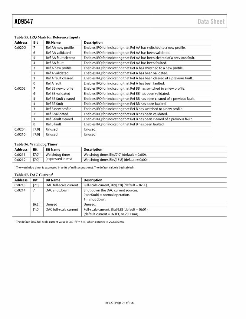
AD9547 Data Sheet
Table 55. IRQ Mask for Reference Inputs Address Bit Bit Name Description 0x020D 7 Ref AA new profile Enables IRQ for indicating that Ref AA has switched to a new profile.
6 Ref AA validated Enables IRQ for indicating that Ref AA has been validated. 5 Ref AA fault cleared Enables IRQ for indicating that Ref AA has been cleared of a previous fault. 4 Ref AA fault Enables IRQ for indicating that Ref AA has been faulted. 3 Ref A new profile Enables IRQ for indicating that Ref A has switched to a new profile. 2 Ref A validated Enables IRQ for indicating that Ref A has been validated. 1 Ref A fault cleared Enables IRQ for indicating that Ref A has been cleared of a previous fault. 0 Ref A fault Enables IRQ for indicating that Ref A has been faulted.
0x020E 7 Ref BB new profile Enables IRQ for indicating that Ref BB has switched to a new profile. 6 Ref BB validated Enables IRQ for indicating that Ref BB has been validated. 5 Ref BB fault cleared Enables IRQ for indicating that Ref BB has been cleared of a previous fault. 4 Ref BB fault Enables IRQ for indicating that Ref BB has been faulted. 3 Ref B new profile Enables IRQ for indicating that Ref B has switched to a new profile. 2 Ref B validated Enables IRQ for indicating that Ref B has been validated. 1 Ref B fault cleared Enables IRQ for indicating that Ref B has been cleared of a previous fault. 0 Ref B fault Enables IRQ for indicating that Ref B has been faulted.
0x020F [7:0] Unused Unused. 0x0210 [7:0] Unused Unused.
Table 56. Watchdog Timer1 Address Bit Bit Name Description 0x0211 [7:0] Watchdog timer
(expressed in ms) Watchdog timer, Bits[7:0] (default = 0x00).
0x0212 [7:0] Watchdog timer, Bits[15:8] (default = 0x00).
1 The watchdog timer is expressed in units of milliseconds (ms). The default value is 0 (disabled).
Table 57. DAC Current1 Address Bit Bit Name Description 0x0213 [7:0] DAC full-scale current Full-scale current, Bits[7:0] (default = 0xFF). 0x0214 7 DAC shutdown Shut down the DAC current sources.
0 (default) = normal operation. 1 = shut down.
[6:2] Unused Unused. [1:0] DAC full-scale current Full-scale current, Bits[9:8] (default = 0b01).
(default current = 0x1FF, or 20.1 mA).
1 The default DAC full-scale current value is 0x01FF = 511, which equates to 20.1375 mA.
Rev. G | Page 74 of 106
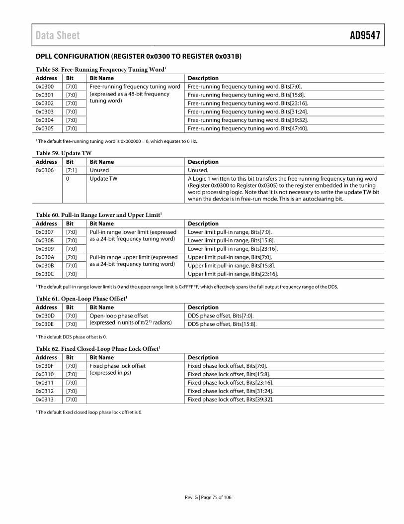
Data Sheet AD9547
DPLL CONFIGURATION (REGISTER 0x0300 TO REGISTER 0x031B)
Table 58. Free-Running Frequency Tuning Word1 Address Bit Bit Name Description 0x0300 [7:0] Free-running frequency tuning word
(expressed as a 48-bit frequency tuning word)
Free-running frequency tuning word, Bits[7:0]. 0x0301 [7:0] Free-running frequency tuning word, Bits[15:8]. 0x0302 [7:0] Free-running frequency tuning word, Bits[23:16]. 0x0303 [7:0] Free-running frequency tuning word, Bits[31:24]. 0x0304 [7:0] Free-running frequency tuning word, Bits[39:32]. 0x0305 [7:0] Free-running frequency tuning word, Bits[47:40].
1 The default free-running tuning word is 0x000000 = 0, which equates to 0 Hz.
Table 59. Update TW Address Bit Bit Name Description 0x0306 [7:1] Unused Unused.
0 Update TW A Logic 1 written to this bit transfers the free-running frequency tuning word (Register 0x0300 to Register 0x0305) to the register embedded in the tuning word processing logic. Note that it is not necessary to write the update TW bit when the device is in free-run mode. This is an autoclearing bit.
Table 60. Pull-in Range Lower and Upper Limit1 Address Bit Bit Name Description 0x0307 [7:0] Pull-in range lower limit (expressed
as a 24-bit frequency tuning word) Lower limit pull-in range, Bits[7:0].
0x0308 [7:0] Lower limit pull-in range, Bits[15:8]. 0x0309 [7:0] Lower limit pull-in range, Bits[23:16]. 0x030A [7:0] Pull-in range upper limit (expressed
as a 24-bit frequency tuning word) Upper limit pull-in range, Bits[7:0].
0x030B [7:0] Upper limit pull-in range, Bits[15:8]. 0x030C [7:0] Upper limit pull-in range, Bits[23:16].
1 The default pull-in range lower limit is 0 and the upper range limit is 0xFFFFFF, which effectively spans the full output frequency range of the DDS.
Table 61. Open-Loop Phase Offset1 Address Bit Bit Name Description 0x030D [7:0] Open-loop phase offset
(expressed in units of π/215 radians) DDS phase offset, Bits[7:0].
0x030E [7:0] DDS phase offset, Bits[15:8].
1 The default DDS phase offset is 0.
Table 62. Fixed Closed-Loop Phase Lock Offset1 Address Bit Bit Name Description 0x030F [7:0] Fixed phase lock offset
(expressed in ps) Fixed phase lock offset, Bits[7:0].
0x0310 [7:0] Fixed phase lock offset, Bits[15:8]. 0x0311 [7:0] Fixed phase lock offset, Bits[23:16]. 0x0312 [7:0] Fixed phase lock offset, Bits[31:24]. 0x0313 [7:0] Fixed phase lock offset, Bits[39:32].
1 The default fixed closed loop phase lock offset is 0.
Rev. G | Page 75 of 106
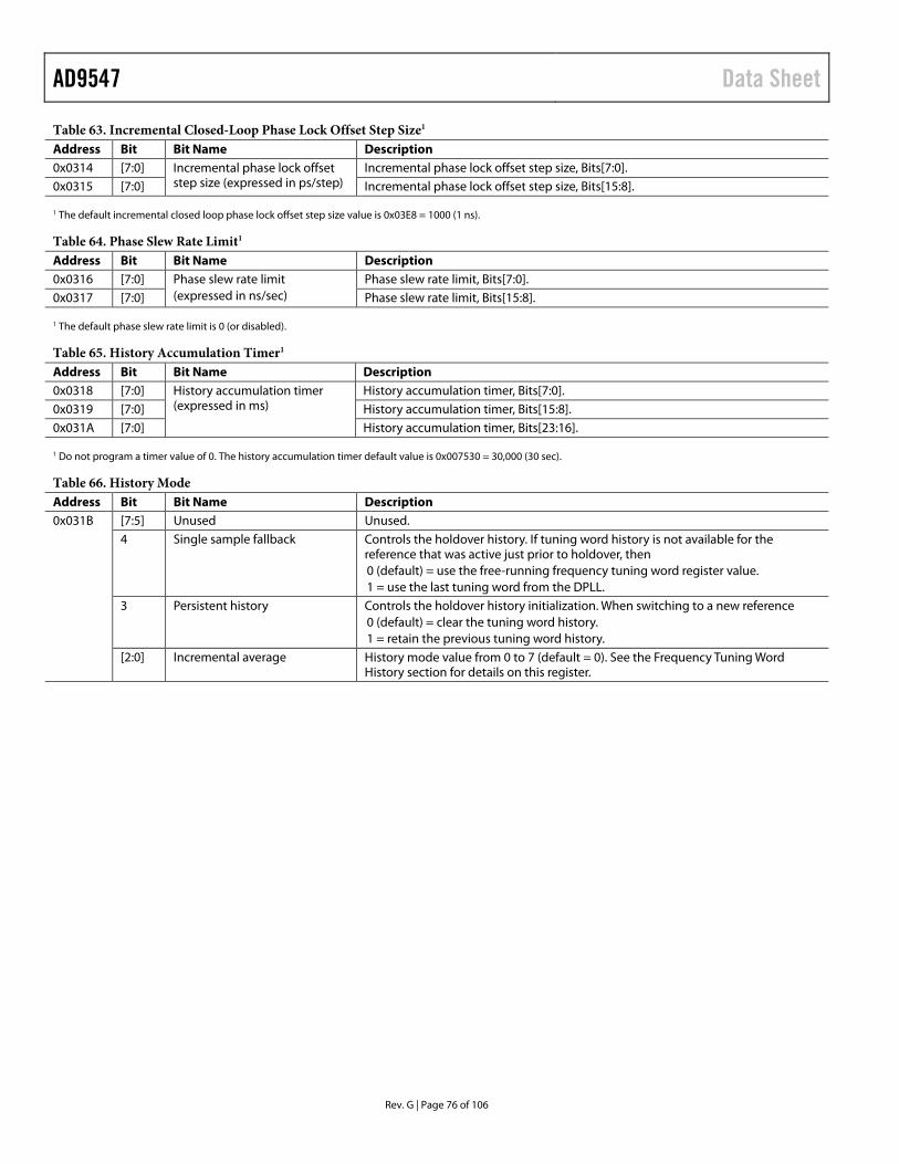
AD9547 Data Sheet
Table 63. Incremental Closed-Loop Phase Lock Offset Step Size1 Address Bit Bit Name Description 0x0314 [7:0] Incremental phase lock offset
step size (expressed in ps/step) Incremental phase lock offset step size, Bits[7:0].
0x0315 [7:0] Incremental phase lock offset step size, Bits[15:8].
1 The default incremental closed loop phase lock offset step size value is 0x03E8 = 1000 (1 ns).
Table 64. Phase Slew Rate Limit1 Address Bit Bit Name Description 0x0316 [7:0] Phase slew rate limit
(expressed in ns/sec) Phase slew rate limit, Bits[7:0].
0x0317 [7:0] Phase slew rate limit, Bits[15:8].
1 The default phase slew rate limit is 0 (or disabled).
Table 65. History Accumulation Timer1 Address Bit Bit Name Description 0x0318 [7:0] History accumulation timer
(expressed in ms) History accumulation timer, Bits[7:0].
0x0319 [7:0] History accumulation timer, Bits[15:8]. 0x031A [7:0] History accumulation timer, Bits[23:16].
1 Do not program a timer value of 0. The history accumulation timer default value is 0x007530 = 30,000 (30 sec).
Table 66. History Mode Address Bit Bit Name Description 0x031B [7:5] Unused Unused.
4 Single sample fallback Controls the holdover history. If tuning word history is not available for the reference that was active just prior to holdover, then 0 (default) = use the free-running frequency tuning word register value. 1 = use the last tuning word from the DPLL.
3 Persistent history Controls the holdover history initialization. When switching to a new reference 0 (default) = clear the tuning word history. 1 = retain the previous tuning word history.
[2:0] Incremental average History mode value from 0 to 7 (default = 0). See the Frequency Tuning Word History section for details on this register.
Rev. G | Page 76 of 106
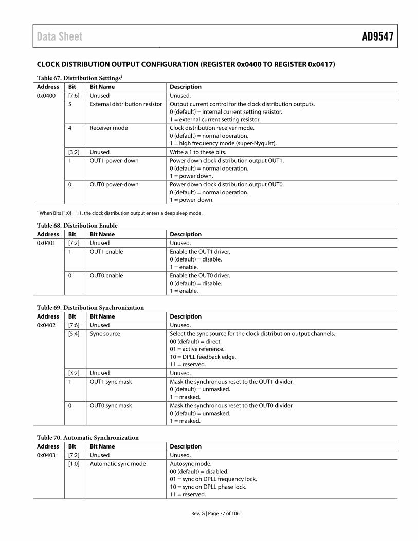
Data Sheet AD9547
CLOCK DISTRIBUTION OUTPUT CONFIGURATION (REGISTER 0x0400 TO REGISTER 0x0417)
Table 67. Distribution Settings1 Address Bit Bit Name Description 0x0400 [7:6] Unused Unused.
5 External distribution resistor Output current control for the clock distribution outputs. 0 (default) = internal current setting resistor. 1 = external current setting resistor.
4 Receiver mode Clock distribution receiver mode. 0 (default) = normal operation. 1 = high frequency mode (super-Nyquist).
[3:2] Unused Write a 1 to these bits. 1 OUT1 power-down Power down clock distribution output OUT1.
0 (default) = normal operation. 1 = power down.
0 OUT0 power-down Power down clock distribution output OUT0. 0 (default) = normal operation. 1 = power-down.
1 When Bits [1:0] = 11, the clock distribution output enters a deep sleep mode.
Table 68. Distribution Enable Address Bit Bit Name Description 0x0401 [7:2] Unused Unused.
1 OUT1 enable Enable the OUT1 driver. 0 (default) = disable. 1 = enable.
0 OUT0 enable Enable the OUT0 driver. 0 (default) = disable. 1 = enable.
Table 69. Distribution Synchronization Address Bit Bit Name Description 0x0402 [7:6] Unused Unused.
[5:4] Sync source Select the sync source for the clock distribution output channels. 00 (default) = direct. 01 = active reference. 10 = DPLL feedback edge. 11 = reserved.
[3:2] Unused Unused. 1 OUT1 sync mask Mask the synchronous reset to the OUT1 divider.
0 (default) = unmasked. 1 = masked.
0 OUT0 sync mask Mask the synchronous reset to the OUT0 divider. 0 (default) = unmasked. 1 = masked.
Table 70. Automatic Synchronization Address Bit Bit Name Description 0x0403 [7:2] Unused Unused.
[1:0] Automatic sync mode Autosync mode. 00 (default) = disabled. 01 = sync on DPLL frequency lock. 10 = sync on DPLL phase lock. 11 = reserved.
Rev. G | Page 77 of 106
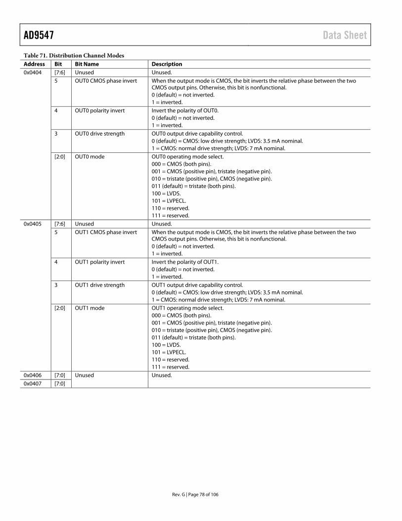
AD9547 Data Sheet Table 71. Distribution Channel Modes Address Bit Bit Name Description 0x0404 [7:6] Unused Unused.
5 OUT0 CMOS phase invert When the output mode is CMOS, the bit inverts the relative phase between the two CMOS output pins. Otherwise, this bit is nonfunctional. 0 (default) = not inverted. 1 = inverted.
4 OUT0 polarity invert Invert the polarity of OUT0. 0 (default) = not inverted. 1 = inverted.
3 OUT0 drive strength OUT0 output drive capability control. 0 (default) = CMOS: low drive strength; LVDS: 3.5 mA nominal. 1 = CMOS: normal drive strength; LVDS: 7 mA nominal.
[2:0] OUT0 mode OUT0 operating mode select. 000 = CMOS (both pins). 001 = CMOS (positive pin), tristate (negative pin). 010 = tristate (positive pin), CMOS (negative pin). 011 (default) = tristate (both pins). 100 = LVDS. 101 = LVPECL. 110 = reserved. 111 = reserved.
0x0405 [7:6] Unused Unused. 5 OUT1 CMOS phase invert When the output mode is CMOS, the bit inverts the relative phase between the two
CMOS output pins. Otherwise, this bit is nonfunctional. 0 (default) = not inverted. 1 = inverted.
4 OUT1 polarity invert Invert the polarity of OUT1. 0 (default) = not inverted. 1 = inverted.
3 OUT1 drive strength OUT1 output drive capability control. 0 (default) = CMOS: low drive strength; LVDS: 3.5 mA nominal. 1 = CMOS: normal drive strength; LVDS: 7 mA nominal.
[2:0] OUT1 mode OUT1 operating mode select. 000 = CMOS (both pins). 001 = CMOS (positive pin), tristate (negative pin). 010 = tristate (positive pin), CMOS (negative pin). 011 (default) = tristate (both pins). 100 = LVDS. 101 = LVPECL. 110 = reserved. 111 = reserved.
0x0406 [7:0] Unused Unused. 0x0407 [7:0]
Rev. G | Page 78 of 106

Data Sheet AD9547
Register 0x0408 to Register 0x0417—Distribution Channel Dividers
Table 72. Q0 Divider1 Address Bit Bit Name Description 0x0408 [7:0] Q0 Q0 divider, Bits[7:0]. 0x0409 [7:0] Q0 divider, Bits[15:8]. 0x040A [7:0] Q0 divider, Bits[23:16]. 0x040B [7:6] Unused Unused.
[5:0] Q0 Q0 divider, Bits[29:24].
1 The default value is 0 (or divide by 1).
Table 73. Q1 Divider1 Address Bit Bit Name Description 0x040C [7:0] Q1 Q1 divider, Bits[7:0]. 0x040D [7:0] Q1 divider, Bits[15:8]. 0x040E [7:0] Q1 divider, Bits[23:16]. 0x040F [7:6] Unused Unused.
[5:0] Q1 Q1 divider, Bits[29:24].
1 The default value is 0 (or divide by 1).
Table 74. Reserved Address Bit Bit Name Description 0x0410 to 0x0417
[7:0] Unused Unused.
REFERENCE INPUT CONFIGURATION (REGISTER 0x0500 TO REGISTER 0x0507) When all bits are set, the reference receiver section enters a deep sleep mode.
Table 75. Reference Power-Down Address Bit Bit Name Description 0x0500 [7:4] Unused Write a 1 to these bits.
3 Ref BB power-down REF BB input receiver power-down. 0 (default) = normal operation. 1 = power-down.
2 Ref B power-down REF B input receiver power-down. 0 (default) = normal operation. 1 = power-down.
1 Ref AA power-down REF AA input receiver power-down. 0 (default) = normal operation. 1 = power-down.
0 Ref A power-down REF A input receiver power-down. 0 (default) = normal operation. 1 = power-down.
Rev. G | Page 79 of 106

AD9547 Data Sheet
Table 76. Reference Logic Family Address Bit Bit Name Description 0x0501 [7:6] Ref BB logic family Select the logic family for the REF BB input receiver (ignored if Bits[5:4] = 00).
00 (default) = disabled. 01 = 1.2 V to 1.5 V CMOS. 10 = 1.8 V to 2.5 V CMOS. 11 = 3.0 V to 3.3 V CMOS.
[5:4] Ref B logic family Select logic family for REF B input receiver. 00 (default) = differential (REFB/BB is positive/negative input). 01 = 1.2 V to 1.5 V CMOS. 10 = 1.8 V to 2.5 V CMOS. 11 = 3.0 V to 3.3 V CMOS.
[3:2] Ref AA logic family The same as Register 0x0501, Bits[7:6] but for REF AA. [1:0] Ref A logic family The same as Register 0x0501, Bits[5:4] but for REF A.
0x0502 [7:0] Unused Unused.
Table 77. Manual Reference Profile Selection Address Bit Bit Name Description 0x0503 7 Enable Ref AA manual profile Select manual or automatic reference profile assignment for REF AA.
0 (default) = automatic. 1 = manual.
[6:4] Ref AA manual profile Manual profile assignment. 000 (default) = Profile 0. 001 = Profile 1. 010 = Profile 2. 011 = Profile 3. 100 = Profile 4. 101 = Profile 5. 110 = Profile 6. 111 = Profile 7.
3 Enable Ref A manual profile Same as Register 0x0503, Bit 7 but for REF A. [2:0] Ref A manual profile Same as Register 0x0503, Bits[6:4] but for REF A.
0x0504 7 Enable Ref BB manual profile Same as Register 0x0503, Bit 7 but for REF BB. [6:4] Ref BB manual profile Same as Register 0x0503, Bits[6:4] but for REF BB. 3 Enable Ref B manual profile Same as Register 0x0503, Bit 7 but for REF B. [2:0] Ref B manual profile Same as Register 0x0503, Bits[6:4] but for REF B.
0x0505 [7:0] Unused Unused. 0x0506 [7:0]
Table 78. Phase Build-Out Switching Address Bit Bit Name Description 0x0507 [7:3] Unused Unused.
[2:0] Phase master threshold priority
Threshold priority level (a value of 0 to 7, with 0 (default) being the highest priority level). References with a selection priority value lower than this value are treated as phase masters (see the profile registers for selection priority value).
Rev. G | Page 80 of 106
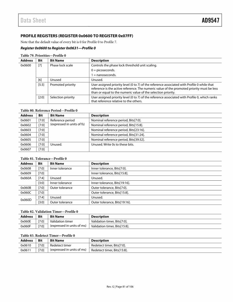
Data Sheet AD9547
PROFILE REGISTERS (REGISTER 0x0600 TO REGISTER 0x07FF) Note that the default value of every bit is 0 for Profile 0 to Profile 7.
Register 0x0600 to Register 0x0631—Profile 0
Table 79. Priorities—Profile 0 Address Bit Bit Name Description 0x0600 [7] Phase lock scale Controls the phase lock threshold unit scaling.
0 = picoseconds. 1 = nanoseconds. [6] Unused Unused. [5:3] Promoted priority User assigned priority level (0 to 7) of the reference associated with Profile 0 while that
reference is the active reference. The numeric value of the promoted priority must be less than or equal to the numeric value of the selection priority.
[2:0] Selection priority User assigned priority level (0 to 7) of the reference associated with Profile 0, which ranks that reference relative to the others.
Table 80. Reference Period—Profile 0 Address Bit Bit Name Description 0x0601 [7:0] Reference period
(expressed in units of fs) Nominal reference period, Bits[7:0].
0x0602 [7:0] Nominal reference period, Bits[15:8]. 0x0603 [7:0] Nominal reference period, Bits[23:16]. 0x0604 [7:0] Nominal reference period, Bits[31:24]. 0x0605 [7:0] Nominal reference period, Bits[39:32]. 0x0606 [7:0] Unused. Unused. Write 0s to these bits. 0x0607 [7:0]
Table 81. Tolerance—Profile 0 Address Bit Bit Name Description 0x0608 [7:0] Inner tolerance Inner tolerance, Bits[7:0]. 0x0609 [7:0] Inner tolerance, Bits[15:8]. 0x060A [7:4] Unused Unused.
[3:0] Inner tolerance Inner tolerance, Bits[19:16]. 0x060B [7:0] Outer tolerance Outer tolerance, Bits[7:0]. 0x060C [7:0] Outer tolerance, Bits[15:8].
0x060D [7:4] Unused Unused. [3:0] Outer tolerance Outer tolerance, Bits[19:16].
Table 82. Validation Timer—Profile 0 Address Bit Bit Name Description 0x060E [7:0] Validation timer
(expressed in units of ms) Validation timer, Bits[7:0].
0x060F [7:0] Validation timer, Bits[15:8].
Table 83. Redetect Timer—Profile 0 Address Bit Bit Name Description 0x0610 [7:0] Redetect timer
(expressed in units of ms) Redetect timer, Bits[7:0].
0x0611 [7:0] Redetect timer, Bits[15:8].
Rev. G | Page 81 of 106

AD9547 Data Sheet
Table 84. Digital Loop Filter Coefficients—Profile 01 Address Bit Bit Name Description 0x0612 [7:0] Alpha-0 linear Alpha-0 coefficient linear, Bits[7:0]. 0x0613 [7:0] Alpha-0 coefficient linear, Bits[15:8]. 0x0614 [7:6] Alpha-2 exponent Alpha-2 coefficient exponent, Bits[1:0].
[5:0] Alpha-1 exponent Alpha-1 coefficient exponent, Bits[5:0]. 0x0615 [7:1] Beta-0 linear Beta-0 coefficient linear, Bits[6:0].
0 Alpha-2 exponent Alpha-2 coefficient exponent, Bit 2. 0x0616 [7:0] Beta-0 linear Beta-0 coefficient linear, Bits[14:7]. 0x0617 7 Unused Unused.
[6:2] Beta-1 exponent Beta-1 coefficient exponent, Bits[4:0]. [1:0] Beta-0 linear Beta-0 coefficient linear, Bits[16:15].
0x0618 [7:0] Gamma-0 linear Gamma-0 coefficient linear, Bits[7:0]. 0x0619 [7:0] Gamma-0 coefficient linear, Bits[15:8]. 0x061A [7:6] Unused Unused.
[5:1] Gamma-1 exponent Gamma-1 coefficient exponent, Bits[4:0]. 0 Gamma-0 linear Gamma-0 coefficient linear, Bit 16.
0x061B [7:0] Delta-0 linear Delta-0 coefficient linear, Bits[7:0]. 0x061C 7 Delta-1 exponent Delta-1 coefficient exponent, Bit 0.
[6:0] Delta-0 linear Delta-0 coefficient linear, Bits[14:8]. 0x061D [7:4] Alpha-3 exponent Alpha-3 coefficient exponent, Bits[3:0].
[3:0] Delta-1 exponent Delta-1 coefficient exponent, Bits[4:1].
1 The digital loop filter coefficients (α, β, γ, and δ) have the general form: x(2y), where x is the linear component and y is the exponential component of the coefficient. The value of the linear component (x) constitutes a fraction, where 0 ≤ x < 1. The exponential component (y) is an integer. See the Calculating the Digital Filter Coefficients section for details.
Register 0x061E to Register 0x0628—Profile 0 Frequency Multiplication
Table 85. R Divider—Profile 01 Address Bit Bit Name Description 0x061E [7:0] R R, Bits[7:0]. 0x061F [7:0] R, Bits[15:8]. 0x0620 [7:0] R, Bits[23:16]. 0x0621 [7:6] Unused Unused.
[5:0] R R, Bits[29:24].
1 The value stored in the R divider register yields an actual divide ratio of one more than the programmed value.
Table 86. S Divider—Profile 01 Address Bit Bit Name Description 0x0622 [7:0] S S, Bits[7:0]. 0x0623 [7:0] S S, Bits[15:8]. 0x0624 [7:4] Unused Unused.
[3:0] S S, Bits[19:16]. 0x0625 [7:0] Unused Unused.
1 The value stored in the S divider register yields an actual divide ratio of one more than the programmed value. Furthermore, the value of S must be at least 7.
Rev. G | Page 82 of 106

Data Sheet AD9547
Table 87. Fractional Feedback Divider—Profile 0 Address Bit Bit Name Description 0x0626 [7:0] V V, Bits[7:0]. 0x0627 [7:4] U U, Bits[3:0].
[3:2] Unused Unused. [1:0] V V, Bits[9:8].
0x0628 [7:6] Unused Unused. [5:0] U U, Bits[9:4].
Table 88. Lock Detectors—Profile 0 Address Bit Bit Name Description 0x0629 [7:0] Phase lock threshold (units determined by Register 0x0600[7]) Phase lock threshold, Bits[7:0]. 0x062A [7:0] Phase lock threshold, Bits[15:8]. 0x062B [7:0] Phase lock fill rate Phase lock fill rate, Bits[7:0]. 0x062C [7:0] Phase lock drain rate Phase lock drain rate, Bits[7:0]. 0x062D [7:0] Frequency lock threshold (expressed in units of ps) Frequency lock threshold, Bits[7:0]. 0x062E [7:0] Frequency lock threshold, Bits[15:8]. 0x062F [7:0] Frequency lock threshold, Bits[23:16]. 0x0630 [7:0] Frequency lock fill rate Frequency lock fill rate, Bits[7:0]. 0x0631 [7:0] Frequency lock drain rate Frequency lock drain rate, Bits[7:0].
Register 0x0632 to Register 0x067F—Profile 1
Table 89. Priorities—Profile 1 Address Bit Bit Name Description 0x0632 [7] Phase lock scale Controls the phase lock threshold unit scaling.
0 = picoseconds. 1 = nanoseconds. [6] Unused Unused. [5:3] Promoted priority User assigned priority level (0 to 7) of the reference associated with Profile 1 while
that reference is the active reference. The numeric value of the promoted priority must be less than or equal to the numeric value of the selection priority.
[2:0] Selection priority User assigned priority level (0 to 7) of the reference associated with Profile 1, which ranks that reference relative to the others.
Table 90. Reference Period—Profile 1 Address Bit Bit Name Description 0x0633 [7:0] Reference period (expressed in units of fs) Nominal reference period, Bits[7:0]. 0x0634 [7:0] Nominal reference period, Bits[15:8]. 0x0635 [7:0] Nominal reference period, Bits[23:16]. 0x0636 [7:0] Nominal reference period, Bits[31:24]. 0x0637 [7:0] Nominal reference period, Bits[39:32]. 0x0638 [7:0] Unused Unused. Write 0s to these bits. 0x0639 [7:0]
Table 91. Tolerance—Profile 1 Address Bit Bit Name Description 0x063A [7:0] Inner tolerance Inner tolerance, Bits[7:0]. 0x063B [7:0] Inner tolerance, Bits[15:8]. 0x063C [7:4] Unused Unused.
[3:0] Inner tolerance Inner tolerance, Bits[19:16]. 0x063D [7:0] Outer tolerance Outer tolerance, Bits[7:0]. 0x063E [7:0] Outer tolerance, Bits[15:8].
Rev. G | Page 83 of 106

AD9547 Data Sheet
Address Bit Bit Name Description 0x063F [7:4] Unused Unused.
[3:0] Outer tolerance Outer tolerance, Bits[19:16].
Table 92. Validation Timer—Profile 1 Address Bit Bit Name Description 0x0640 [7:0] Validation timer
(expressed in units of ms) Validation timer, Bits[7:0].
0x0641 [7:0] Validation timer, Bits[15:8].
Table 93. Redetect Timer—Profile 1 Address Bit Bit Name Description 0x0642 [7:0] Redetect timer
(expressed in units of ms) Redetect timer, Bits[7:0].
0x0643 [7:0] Redetect timer, Bits[15:8].
Table 94. Digital Loop Filter Coefficients—Profile 11 Address Bit Bit Name Description 0x0644 [7:0] Alpha-0 linear Alpha-0 coefficient linear, Bits[7:0]. 0x0645 [7:0] Alpha-0 coefficient linear, Bits[15:8]. 0x0646 [7:6] Alpha-2 exponent Alpha-2 coefficient exponent, Bits[1:0].
[5:0] Alpha-1 exponent Alpha-1 coefficient exponent, Bits[5:0]. 0x0647 [7:1] Beta-0 linear Beta-0 coefficient linear, Bits[6:0].
0 Alpha-2 exponent Alpha-2 coefficient exponent, Bit 2. 0x0648 [7:0] Beta-0 linear Beta-0 coefficient linear, Bits[14:7]. 0x0649 7 Unused Unused.
[6:2] Beta-1 exponent Beta-1 coefficient exponent, Bits[4:0]. [1:0] Beta-0 linear Beta-0 coefficient linear, Bits[16:15].
0x064A [7:0] Gamma-0 linear Gamma-0 coefficient linear, Bits[7:0]. 0x064B [7:0] Gamma-0 coefficient linear, Bits[15:8]. 0x064C [7:6] Unused Unused.
[5:1] Gamma-1 exponent Gamma-1 coefficient exponent, Bits[4:0]. 0 Gamma-0 linear Gamma-0 coefficient linear, Bit 16.
0x064D [7:0] Delta-0 linear Delta-0 coefficient linear, Bits[7:0]. 0x064E 7 Delta-1 exponent Delta-1 coefficient exponent, Bit 0.
[6:0] Delta-0 linear Delta-0 coefficient linear, Bits[14:8]. 0x064F [7:4] Alpha-3 exponent Alpha-3 coefficient exponent, Bits[3:0].
[3:0] Delta-1 exponent Delta-1 coefficient exponent, Bits[4:1].
1 The digital loop filter coefficients (α, β, γ, and δ) have the general form: x(2y), where x is the linear component and y is the exponential component of the coefficient. The value of the linear component (x) constitutes a fraction, where 0 ≤ x < 1. The exponential component (y) is an integer. See the Calculating the Digital Filter Coefficients section for details.
Register 0x0650 to Register 0x065A—Profile 1 Frequency Multiplication
Table 95. R Divider—Profile 11 Address Bit Bit Name Description 0x0650 [7:0] R R, Bits[7:0]. 0x0651 [7:0] R, Bits[15:8]. 0x0652 [7:0] R, Bits[23:16]. 0x0653 [7:6] Unused Unused.
[5:0] R R, Bits[29:24].
1 The value stored in the R divider register yields an actual divide ratio of one more than the programmed value.
Rev. G | Page 84 of 106
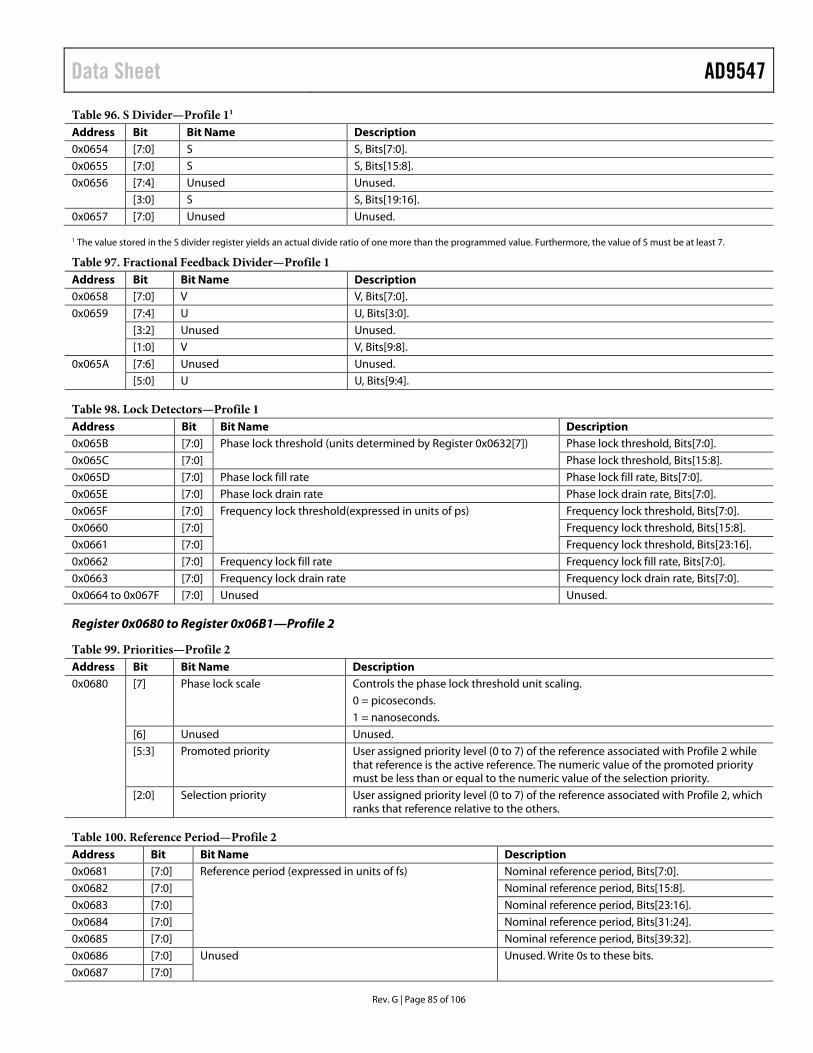
Data Sheet AD9547
Table 96. S Divider—Profile 11 Address Bit Bit Name Description 0x0654 [7:0] S S, Bits[7:0]. 0x0655 [7:0] S S, Bits[15:8]. 0x0656 [7:4] Unused Unused.
[3:0] S S, Bits[19:16]. 0x0657 [7:0] Unused Unused.
1 The value stored in the S divider register yields an actual divide ratio of one more than the programmed value. Furthermore, the value of S must be at least 7.
Table 97. Fractional Feedback Divider—Profile 1 Address Bit Bit Name Description 0x0658 [7:0] V V, Bits[7:0]. 0x0659 [7:4] U U, Bits[3:0].
[3:2] Unused Unused. [1:0] V V, Bits[9:8].
0x065A [7:6] Unused Unused. [5:0] U U, Bits[9:4].
Table 98. Lock Detectors—Profile 1 Address Bit Bit Name Description 0x065B [7:0] Phase lock threshold (units determined by Register 0x0632[7]) Phase lock threshold, Bits[7:0]. 0x065C [7:0] Phase lock threshold, Bits[15:8]. 0x065D [7:0] Phase lock fill rate Phase lock fill rate, Bits[7:0]. 0x065E [7:0] Phase lock drain rate Phase lock drain rate, Bits[7:0]. 0x065F [7:0] Frequency lock threshold(expressed in units of ps) Frequency lock threshold, Bits[7:0]. 0x0660 [7:0] Frequency lock threshold, Bits[15:8]. 0x0661 [7:0] Frequency lock threshold, Bits[23:16]. 0x0662 [7:0] Frequency lock fill rate Frequency lock fill rate, Bits[7:0]. 0x0663 [7:0] Frequency lock drain rate Frequency lock drain rate, Bits[7:0]. 0x0664 to 0x067F [7:0] Unused Unused.
Register 0x0680 to Register 0x06B1—Profile 2
Table 99. Priorities—Profile 2 Address Bit Bit Name Description 0x0680 [7] Phase lock scale Controls the phase lock threshold unit scaling.
0 = picoseconds. 1 = nanoseconds. [6] Unused Unused. [5:3] Promoted priority User assigned priority level (0 to 7) of the reference associated with Profile 2 while
that reference is the active reference. The numeric value of the promoted priority must be less than or equal to the numeric value of the selection priority.
[2:0] Selection priority User assigned priority level (0 to 7) of the reference associated with Profile 2, which ranks that reference relative to the others.
Table 100. Reference Period—Profile 2 Address Bit Bit Name Description 0x0681 [7:0] Reference period (expressed in units of fs) Nominal reference period, Bits[7:0]. 0x0682 [7:0] Nominal reference period, Bits[15:8]. 0x0683 [7:0] Nominal reference period, Bits[23:16]. 0x0684 [7:0] Nominal reference period, Bits[31:24]. 0x0685 [7:0] Nominal reference period, Bits[39:32]. 0x0686 [7:0] Unused Unused. Write 0s to these bits. 0x0687 [7:0]
Rev. G | Page 85 of 106

AD9547 Data Sheet Table 101. Tolerance—Profile 2 Address Bit Bit Name Description 0x0688 [7:0] Inner tolerance Inner tolerance, Bits[7:0]. 0x0689 [7:0] Inner tolerance, Bits[15:8]. 0x068A [7:4] Unused Unused.
[3:0] Inner tolerance Inner tolerance, Bits[19:16]. 0x068B [7:0] Outer tolerance Outer tolerance, Bits[7:0]. 0x068C [7:0] Outer tolerance, Bits[15:8]. 0x068D [7:4] Unused Unused.
[3:0] Outer tolerance Outer tolerance, Bits[19:16].
Table 102. Validation Timer—Profile 2 Address Bit Bit Name Description 0x068E [7:0] Validation timer
(expressed in units of ms) Validation timer, Bits[7:0].
0x068F [7:0] Validation timer, Bits[15:8].
Table 103. Redetect Timer—Profile 2 Address Bit Bit Name Description 0x0690 [7:0] Redetect timer
(expressed in units of ms) Redetect timer, Bits[7:0].
0x0691 [7:0] Redetect timer, Bits[15:8].
Table 104. Digital Loop Filter Coefficients—Profile 21 Address Bit Bit Name Description 0x0692 [7:0] Alpha-0 linear Alpha-0 coefficient linear, Bits[7:0]. 0x0693 [7:0] Alpha-0 coefficient linear, Bits[15:8]. 0x0694 [7:6] Alpha-2 exponent Alpha-2 coefficient exponent, Bits[1:0].
[5:0] Alpha-1 exponent Alpha-1 coefficient exponent, Bits[5:0]. 0x0695 [7:1] Beta-0 linear Beta-0 coefficient linear, Bits[6:0].
0 Alpha-2 exponent Alpha-2 coefficient exponent, Bit 2. 0x0696 [7:0] Beta-0 linear Beta-0 coefficient linear, Bits[14:7]. 0x0697 7 Unused Unused.
[6:2] Beta-1 exponent Beta-1 coefficient exponent, Bits[4:0]. [1:0] Beta-0 linear Beta-0 coefficient linear, Bits[16:15].
0x0698 [7:0] Gamma-0 linear Gamma-0 coefficient linear, Bits[7:0]. 0x0699 [7:0] Gamma-0 coefficient linear, Bits[15:8]. 0x069A [7:6] Unused Unused.
[5:1] Gamma-1 exponent Gamma-1 coefficient exponent, Bits[4:0]. 0 Gamma-0 linear Gamma-0 coefficient linear, Bit 16.
0x069B [7:0] Delta-0 linear Delta-0 coefficient linear, Bits[7:0]. 0x069C 7 Delta-1 exponent Delta-1 coefficient exponent, Bit 0.
[6:0] Delta-0 linear Delta-0 coefficient linear, Bits[14:8]. 0x069D [7:4] Alpha-3 exponent Alpha-3 coefficient exponent, Bits[3:0].
[3:0] Delta-1 exponent Delta-1 coefficient exponent, Bits[4:1].
1 The digital loop filter coefficients (α, β, γ, and δ) have the general form: x(2y), where x is the linear component and y is the exponential component of the coefficient. The value of the linear component (x) constitutes a fraction, where 0 ≤ x < 1. The exponential component (y) is an integer (see the Calculating the Digital Filter Coefficients section for details).
Rev. G | Page 86 of 106
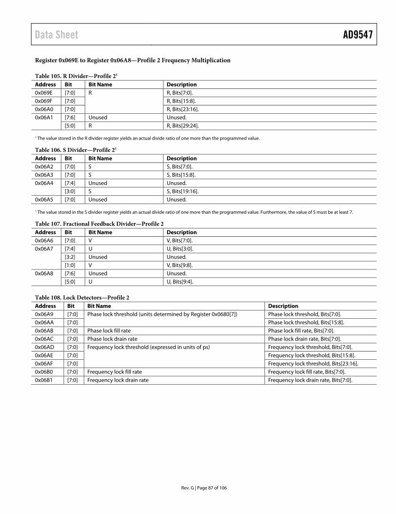
Data Sheet AD9547
Register 0x069E to Register 0x06A8—Profile 2 Frequency Multiplication
Table 105. R Divider—Profile 21 Address Bit Bit Name Description 0x069E [7:0] R R, Bits[7:0]. 0x069F [7:0] R, Bits[15:8]. 0x06A0 [7:0] R, Bits[23:16]. 0x06A1 [7:6] Unused Unused.
[5:0] R R, Bits[29:24].
1 The value stored in the R divider register yields an actual divide ratio of one more than the programmed value.
Table 106. S Divider—Profile 21 Address Bit Bit Name Description 0x06A2 [7:0] S S, Bits[7:0]. 0x06A3 [7:0] S S, Bits[15:8]. 0x06A4 [7:4] Unused Unused.
[3:0] S S, Bits[19:16]. 0x06A5 [7:0] Unused Unused.
1 The value stored in the S divider register yields an actual divide ratio of one more than the programmed value. Furthermore, the value of S must be at least 7.
Table 107. Fractional Feedback Divider—Profile 2 Address Bit Bit Name Description 0x06A6 [7:0] V V, Bits[7:0]. 0x06A7 [7:4] U U, Bits[3:0].
[3:2] Unused Unused. [1:0] V V, Bits[9:8].
0x06A8 [7:6] Unused Unused. [5:0] U U, Bits[9:4].
Table 108. Lock Detectors—Profile 2 Address Bit Bit Name Description 0x06A9 [7:0] Phase lock threshold (units determined by Register 0x0680[7]) Phase lock threshold, Bits[7:0]. 0x06AA [7:0] Phase lock threshold, Bits[15:8]. 0x06AB [7:0] Phase lock fill rate Phase lock fill rate, Bits[7:0]. 0x06AC [7:0] Phase lock drain rate Phase lock drain rate, Bits[7:0]. 0x06AD [7:0] Frequency lock threshold (expressed in units of ps) Frequency lock threshold, Bits[7:0]. 0x06AE [7:0] Frequency lock threshold, Bits[15:8]. 0x06AF [7:0] Frequency lock threshold, Bits[23:16]. 0x06B0 [7:0] Frequency lock fill rate Frequency lock fill rate, Bits[7:0]. 0x06B1 [7:0] Frequency lock drain rate Frequency lock drain rate, Bits[7:0].
Rev. G | Page 87 of 106

AD9547 Data Sheet
Register 0x06B2 to Register 0x06FF—Profile 3
Table 109. Priorities—Profile 3 Address Bit Bit Name Description 0x06B2 [7] Phase lock scale Controls the phase lock threshold unit scaling.
0 = picoseconds. 1 = nanoseconds. [6] Unused Unused. [5:3] Promoted priority User assigned priority level (0 to 7) of the reference associated with Profile 3 while
that reference is the active reference. The numeric value of the promoted priority must be less than or equal to the numeric value of the selection priority.
[2:0] Selection priority User assigned priority level (0 to 7) of the reference associated with Profile 3, which ranks that reference relative to the others.
Table 110. Reference Period—Profile 3 Address Bit Bit Name Description 0x06B3 [7:0] Reference period
(expressed in units of fs) Nominal reference period, Bits[7:0].
0x06B4 [7:0] Nominal reference period, Bits[15:8]. 0x06B5 [7:0] Nominal reference period, Bits[23:16]. 0x06B6 [7:0] Nominal reference period, Bits[31:24]. 0x06B7 [7:0] Nominal reference period, Bits[39:32]. 0x06B8 [7:0] Unused Unused. Write 0s to these bits. 0x06B9 [7:0]
Table 111. Tolerance—Profile 3 Address Bit Bit Name Description 0x06BA [7:0] Inner tolerance Inner tolerance, Bits[7:0]. 0x06BB [7:0] Inner tolerance, Bits[15:8]. 0x06BC [7:4] Unused Unused.
[3:0] Inner tolerance Inner tolerance, Bits[19:16]. 0x06BD [7:0] Outer tolerance Outer tolerance, Bits[7:0]. 0x06BE [7:0] Outer tolerance, Bits[15:8]. 0x06BF [7:4] Unused Unused.
[3:0] Outer tolerance Outer tolerance, Bits[19:16].
Table 112. Validation Timer—Profile 3 Address Bit Bit Name Description 0x06C0 [7:0] Validation timer
(expressed in units of ms) Validation timer, Bits[7:0].
0x06C1 [7:0] Validation timer, Bits[15:8].
Table 113. Redetect Timer—Profile 3 Address Bit Bit Name Description 0x06C2 [7:0] Redetect timer
(expressed in units of ms) Redetect timer, Bits[7:0].
0x06C3 [7:0] Redetect timer, Bits[15:8].
Table 114. Digital Loop Filter Coefficients—Profile 31 Address Bit Bit Name Description 0x06C4 [7:0] Alpha-0 linear Alpha-0 coefficient linear, Bits[7:0]. 0x06C5 [7:0] Alpha-0 coefficient linear, Bits[15:8]. 0x06C6 [7:6] Alpha-2 exponent Alpha-2 coefficient exponent, Bits[1:0].
[5:0] Alpha-1 exponent Alpha-1 coefficient exponent, Bits[5:0]. 0x06C7 [7:1] Beta-0 linear Beta-0 coefficient linear, Bits[6:0].
0 Alpha-2 exponent Alpha-2 coefficient exponent, Bit 2.
Rev. G | Page 88 of 106

Data Sheet AD9547
Address Bit Bit Name Description 0x06C8 [7:0] Beta-0 linear Beta-0 coefficient linear, Bits[14:7]. 0x06C9 7 Unused Unused.
[6:2] Beta-1 exponent Beta-1 coefficient exponent, Bits[4:0]. [1:0] Beta-0 linear Beta-0 coefficient linear, Bits[16:15].
0x06CA [7:0] Gamma-0 linear Gamma-0 coefficient linear, Bits[7:0]. 0x06CB [7:0] Gamma-0 coefficient linear, Bits[15:8]. 0x06CC [7:6] Unused Unused.
[5:1] Gamma-1 exponent Gamma-1 coefficient exponent, Bits[4:0]. 0 Gamma-0 linear Gamma-0 coefficient linear, Bit 16.
0x06CD [7:0] Delta-0 linear Delta-0 coefficient linear, Bits[7:0]. 0x06CE 7 Delta-1 exponent Delta-1 coefficient exponent, Bit 0.
[6:0] Delta-0 linear Delta-0 coefficient linear, Bits[14:8]. 0x06CF [7:4] Alpha-3 exponent Alpha-3 coefficient exponent, Bits[3:0].
[3:0] Delta-1 exponent Delta-1 coefficient exponent, Bits[4:1].
1 The digital loop filter coefficients (α, β, γ, and δ) have the general form: x(2y), where x is the linear component and y is the exponential component of the coefficient. The value of the linear component (x) constitutes a fraction, where 0 ≤ x < 1. The exponential component (y) is an integer (see the Calculating the Digital Filter Coefficients section for details).
Register 0x06D0 to Register 0x06DA—Profile 3 Frequency Multiplication
Table 115. R Divider—Profile 31 Address Bit Bit Name Description 0x06D0 [7:0] R R, Bits[7:0]. 0x06D1 [7:0] R, Bits[15:8]. 0x06D2 [7:0] R, Bits[23:16]. 0x06D3 [7:6] Unused Unused.
[5:0] R R, Bits[29:24].
1 The value stored in the R divider register yields an actual divide ratio of one more than the programmed value.
Table 116. S Divider—Profile 31 Address Bit Bit Name Description 0x06D4 [7:0] S S, Bits[7:0]. 0x06D5 [7:0] S S, Bits[15:8]. 0x06D6 [7:4] Unused Unused.
[3:0] S S, Bits[19:16]. 0x06D7 [7:0] Unused Unused.
1 The value stored in the S divider register yields an actual divide ratio of one more than the programmed value. Furthermore, the value of S must be at least 7.
Table 117. Fractional Feedback Divider—Profile 3 Address Bit Bit Name Description 0x06D8 [7:0] V V, Bits[7:0]. 0x06D9 [7:4] U U, Bits[3:0].
[3:2] Unused Unused. [1:0] V V, Bits[9:8].
0x06DA [7:6] Unused Unused. [5:0] U U, Bits[9:4].
Rev. G | Page 89 of 106
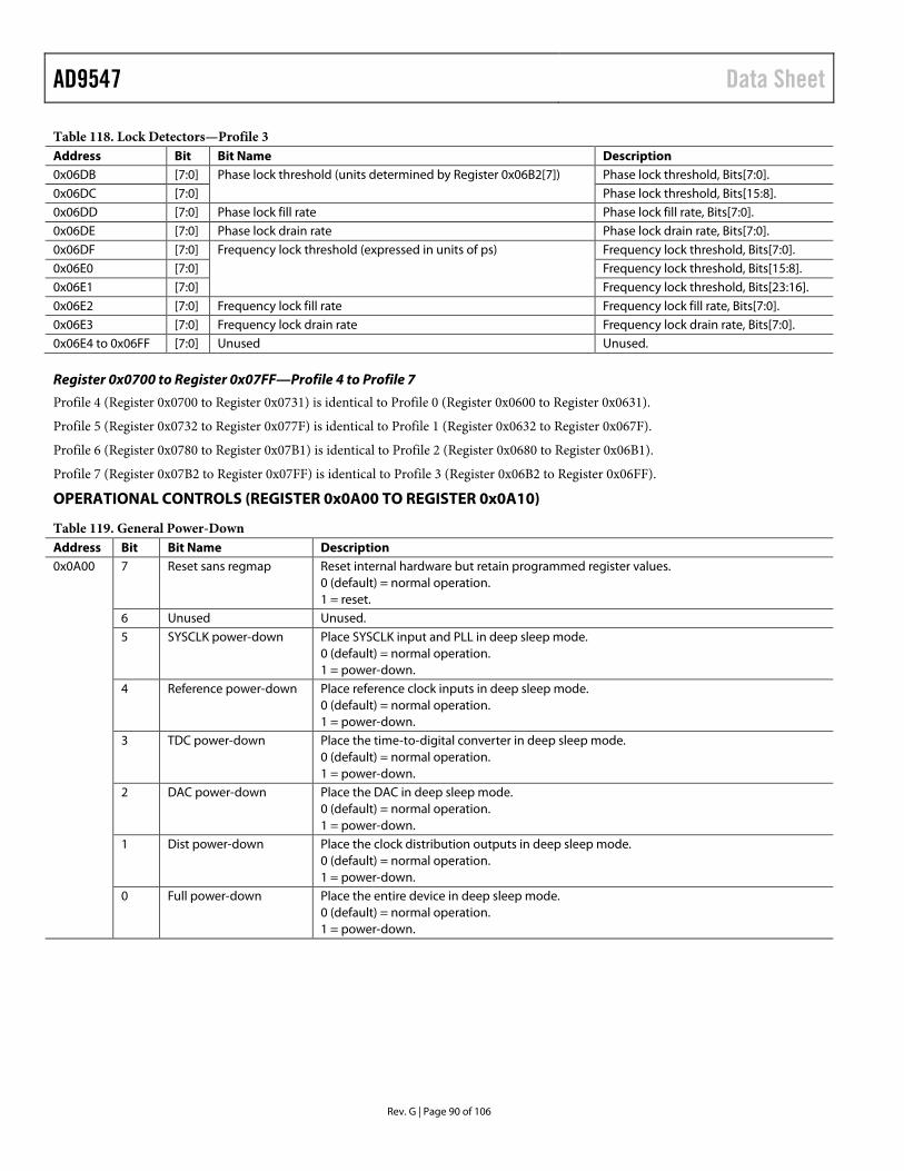
AD9547 Data Sheet
Table 118. Lock Detectors—Profile 3 Address Bit Bit Name Description 0x06DB [7:0] Phase lock threshold (units determined by Register 0x06B2[7]) Phase lock threshold, Bits[7:0]. 0x06DC [7:0] Phase lock threshold, Bits[15:8]. 0x06DD [7:0] Phase lock fill rate Phase lock fill rate, Bits[7:0]. 0x06DE [7:0] Phase lock drain rate Phase lock drain rate, Bits[7:0]. 0x06DF [7:0] Frequency lock threshold (expressed in units of ps) Frequency lock threshold, Bits[7:0]. 0x06E0 [7:0] Frequency lock threshold, Bits[15:8]. 0x06E1 [7:0] Frequency lock threshold, Bits[23:16]. 0x06E2 [7:0] Frequency lock fill rate Frequency lock fill rate, Bits[7:0]. 0x06E3 [7:0] Frequency lock drain rate Frequency lock drain rate, Bits[7:0]. 0x06E4 to 0x06FF [7:0] Unused Unused.
Register 0x0700 to Register 0x07FF—Profile 4 to Profile 7
Profile 4 (Register 0x0700 to Register 0x0731) is identical to Profile 0 (Register 0x0600 to Register 0x0631).
Profile 5 (Register 0x0732 to Register 0x077F) is identical to Profile 1 (Register 0x0632 to Register 0x067F).
Profile 6 (Register 0x0780 to Register 0x07B1) is identical to Profile 2 (Register 0x0680 to Register 0x06B1).
Profile 7 (Register 0x07B2 to Register 0x07FF) is identical to Profile 3 (Register 0x06B2 to Register 0x06FF).
OPERATIONAL CONTROLS (REGISTER 0x0A00 TO REGISTER 0x0A10)
Table 119. General Power-Down Address Bit Bit Name Description 0x0A00 7 Reset sans regmap Reset internal hardware but retain programmed register values.
0 (default) = normal operation. 1 = reset.
6 Unused Unused. 5 SYSCLK power-down Place SYSCLK input and PLL in deep sleep mode.
0 (default) = normal operation. 1 = power-down.
4 Reference power-down Place reference clock inputs in deep sleep mode. 0 (default) = normal operation. 1 = power-down.
3 TDC power-down Place the time-to-digital converter in deep sleep mode. 0 (default) = normal operation. 1 = power-down.
2 DAC power-down Place the DAC in deep sleep mode. 0 (default) = normal operation. 1 = power-down.
1 Dist power-down Place the clock distribution outputs in deep sleep mode. 0 (default) = normal operation. 1 = power-down.
0 Full power-down Place the entire device in deep sleep mode. 0 (default) = normal operation. 1 = power-down.
Rev. G | Page 90 of 106

Data Sheet AD9547
Table 120. Loop Mode Address Bit Bit Name Description 0x0A01 7 Unused Unused.
6 User holdover Force the device into holdover mode. 0 (default) = normal operation. 1 = force device into holdover mode. The device functions as though all input references are faulted.
5 User free run Force the device into free-run mode. 0 (default) = normal operation. 1 = force device into free-run mode. The free-running frequency tuning word register (Address 0x0300 to Address 0x0305) specifies the DDS output frequency. Note that, when user free run is set, it overrides user holdover.
[4:3] User selection mode Select the operating mode of the reference switching state machine. 00 (default) = automatic mode. The fully automatic priority-based algorithm selects the active reference (Bits[1:0] are ignored). 01 = fallback mode. The active reference is the user reference (Bits[1:0]) as long as it is valid. Otherwise, use the fully automatic priority-based algorithm to select the active reference. 10 = holdover mode. The active reference is the user reference (Bits[1:0]) as long as it is valid. Otherwise, enter holdover mode. 11 = manual mode. The active reference is always the user reference (Bits[1:0]). When using manual mode, be sure that the reference declared as the user reference (Bits[1:0]) is programmed for manual reference-to-profile assignment in the appropriate manual reference profile selection register (Address 0x0503 and Address 0x0506).
2 Unused Unused. Write a 0 to this bit. [1:0] User reference selection Input reference when user selection mode = 01, 10, or 11.
00 (default) = Input Reference A. 01 = Input Reference AA. 10 = Input Reference B. 11 = Input Reference BB.
Table 121. Cal/Sync Address Bit Bit Name Description 0x0A02 [7:2] Unused Unused.
1 Sync distribution Setting this bit (default = 0) initiates synchronization of the clock distribution output. When this bit = 1, the clock distribution output stalls. Synchronization occurs on the 1 to 0 transition of this bit.
0 Calibrate SYSCLK A 0 to 1 transition of this bit (default = 0), followed by an IO_UPDATE, initiates an internal calibration of the SYSCLK PLL (assuming it is enabled). The calibration routine automatically selects the proper VCO frequency band and signal amplitude. The internal system clock stalls during the calibration procedure, disabling the device until the calibration is complete (a few milliseconds). If the user wishes to recalibrate the SYSCLK PLL and this bit is already set to 1, the user must first write a 0 to this bit, issue an IO_UPDATE, write a 1 to this bit, and issue another IO_UPDATE.
Rev. G | Page 91 of 106

AD9547 Data Sheet
Register 0x0A03—Reset Functions
Table 122. Reset Functions1 Address Bit Bit Name Description 0x0A03 7 Unused Unused.
6 Clear LF Setting this bit (default = 0) clears the digital loop filter (intended as a debug tool). 5 Clear CCI Setting this bit (default = 0) clears the CCI filter (intended as a debug tool). 4 Clear phase accumulator Setting this bit (default = 0) clears DDS phase accumulator (not a recommended action). 3 Reset auto sync Setting this bit (default = 0) resets the automatic synchronization logic (see Register 0x0403). 2 Reset TW history Setting this bit (default = 0) resets the tuning word history logic (part of holdover
functionality). 1 Reset all IRQs Setting this bit (default = 0) clears the entire IRQ monitor register (Register 0x0D02 to
Register 0x0D09). It is the equivalent of setting all the bits of the IRQ clearing register (Register 0x0A04 to Register 0x0A0B).
0 Reset watchdog Setting this bit (default = 0) resets the watchdog timer (see Register 0x0211 to Register 0x0212). If the timer times out, it simply starts a new timing cycle. If the timer has not yet timed out, it restarts at Time 0 without causing a timeout event. Continuously resetting the watchdog timer at intervals less than its timeout period prevents the watchdog timer from generating a timeout event.
1 All bits in this register are autoclearing.
Register 0x0A04 to Register 0x0A0B—IRQ Clearing
The IRQ clearing registers are identical in format to the IRQ monitor registers (Address 0x0D02 to Address 0x0D09). When set to Logic 1, an IRQ clearing bit resets the corresponding IRQ monitor bit, thereby canceling the interrupt request for the indicated event. The IRQ clearing register is an autoclearing register.
Table 123. IRQ Clearing for SYSCLK Address Bit Bit Name Description 0x0A04 [7:6] Unused Unused.
5 SYSCLK unlocked Clears SYSCLK unlocked IRQ. 4 SYSCLK locked Clears SYSCLK locked IRQ. [3:2] Unused Unused. 1 SYSCLK cal complete Clears SYSCLK calibration complete IRQ. 0 SYSCLK cal started Clears SYSCLK calibration started IRQ.
Table 124. IRQ Clearing for Distribution Sync, Watchdog Timer, and EEPROM Address Bit Bit Name Description 0x0A05 [7:4] Unused Unused.
3 Distribution sync Clears distribution sync IRQ. 2 Watchdog timer Clears watchdog timer IRQ. 1 EEPROM fault Clears EEPROM fault IRQ. 0 EEPROM complete Clears EEPROM complete IRQ.
Table 125. IRQ Clearing for the Digital PLL Address Bit Bit Name Description 0x0A06 7 Switching Clears switching IRQ.
6 Closed Clears closed IRQ. 5 Free run Clears free-run IRQ. 4 Holdover Clears holdover IRQ. 3 Frequency unlocked Clears frequency unlocked IRQ. 2 Frequency locked Clears frequency locked IRQ. 1 Phase unlocked Clears phase unlocked IRQ. 0 Phase locked Clears phase locked IRQ.
Rev. G | Page 92 of 106

Data Sheet AD9547 Table 126. IRQ Clearing for History Update, Frequency Limit, and Phase Slew Limit Address Bit Bit Name Description 0x0A07 [7:5] Unused Unused.
4 History updated Clears history updated IRQ. 3 Frequency unclamped Clears frequency unclamped IRQ. 2 Frequency clamped Clears frequency clamped IRQ. 1 Phase slew unlimited Clears phase slew unlimited IRQ. 0 Phase slew limited Clears phase slew limited IRQ.
Table 127. IRQ Clearing for Reference Inputs Address Bit Bit Name Description 0x0A08 7 Ref AA new profile Clears Ref AA new profile IRQ.
6 Ref AA validated Clears Ref AA validated IRQ. 5 Ref AA fault cleared Clears Ref AA fault cleared IRQ. 4 Ref AA fault Clears Ref AA fault IRQ. 3 Ref A new profile Clears Ref A new profile IRQ. 2 Ref A validated Clears Ref A validated IRQ. 1 Ref A fault cleared Clears Ref A fault cleared IRQ. 0 Ref A fault Clears Ref A fault IRQ.
0x0A09 7 Ref BB new profile Clears Ref BB new profile IRQ. 6 Ref BB validated Clears Ref BB validated IRQ. 5 Ref BB fault cleared Clears Ref BB fault cleared IRQ. 4 Ref BB fault Clears Ref BB fault IRQ. 3 Ref B new profile Clears Ref B new profile IRQ. 2 Ref B validated Clears Ref B validated IRQ. 1 Ref B fault cleared Clears Ref B fault cleared IRQ. 0 Ref B fault Clears Ref B fault IRQ.
0x0A0A [7:0] Unused Unused. 0x0A0B [7:0]
Table 128. Incremental Phase Offset Control Address Bit Bit Name Description 0x0A0C [7:3] Unused Unused.
2 Reset phase offset Resets the incremental phase offset to 0. This is an autoclearing bit. 1 Decrement phase
offset Decrements the incremental phase offset by the amount specified in the incremental phase lock offset step size register (Register 0x0314 to Register 0x0315). This is an autoclearing bit.
0 Increment phase offset
Increments the incremental phase offset by the amount specified in the incremental phase lock offset step size register (Register 0x0314 to Register 0x0315). This is an autoclearing bit.
Table 129. Reference Profile Selection State Machine Startup1 Address Bit Bit Name Description 0x0A0D [7:4] Unused Unused.
3 Detect BB Setting this bit starts the profile selection state machine for Input Reference BB. 2 Detect B Setting this bit starts the profile selection state machine for Input Reference B. 1 Detect AA Setting this bit starts the profile selection state machine for Input Reference AA. 0 Detect A Setting this bit starts the profile selection state machine for Input Reference A.
1 All bits in this register are autoclearing.
Rev. G | Page 93 of 106

AD9547 Data Sheet
Register 0x0A0E to Register 0x0A10—Reference Validation Override Controls
Table 130. Force Validation Timeout1 Address Bit Bit Name Description 0x0A0E [7:4] Unused Unused.
3 Force Timeout BB Setting this bit emulates timeout of the validation timer for Reference BB. This is an autoclearing bit.
2 Force Timeout B Setting this bit emulates timeout of the validation timer for Reference B. This is an autoclearing bit.
1 Force Timeout AA Setting this bit emulates timeout of the validation timer for Reference AA. This is an autoclearing bit.
0 Force Timeout A Setting this bit emulates timeout of the validation timer for Reference A. This is an autoclearing bit.
1 All bits in this register are autoclearing.
Table 131. Reference Monitor Override1 Address Bit Bit Name Description 0x0A0F [7:4] Unused Unused.
3 Ref Mon Override BB Overrides the reference monitor REF fault signal for Reference BB (default = 0, not overridden). 2 Ref Mon Override B Overrides the reference monitor REF fault signal for Reference B (default = 0, not overridden). 1 Ref Mon Override AA Overrides the reference monitor REF fault signal for Reference AA (default = 0, not overridden). 0 Ref Mon Override A Overrides the reference monitor REF fault signal for Reference A (default = 0, not overridden).
1 All bits in this register are autoclearing.
Table 132. Reference Monitor Bypass1 Address Bit Bit Name Description 0x0A10 [7:4] Unused Unused.
3 Ref Mon Bypass BB Bypasses the reference monitor for Reference BB (default = 0, not bypassed). 2 Ref Mon Bypass B Bypasses the reference monitor for Reference B (default = 0, not bypassed). 1 Ref Mon Bypass AA Bypasses the reference monitor for Reference AA (default = 0, not bypassed). 0 Ref Mon Bypass A Bypasses the reference monitor for Reference A (default = 0, not bypassed).
1 All bits in this register are autoclearing.
CLOCK PART SERIAL ID (REGISTER 0x0C00 TO REGISTER 0x0C07) User programmable EEPROM ID registers.
Table 133. User Defined Identification Registers Address Bits Bit Name Description 0x0C00 [7:0] User scratch pad[7:0] User programmable EEPROM ID registers. These registers enable users to write a unique
code of their choosing to keep track of revisions to the EEPROM register loading. It has no effect on part operation. The default EEPROM storage sequence must be altered to include these registers. See the Programming the EEPROM to Include a Clock Part ID section. 0 = default.
0x0C01 [7:0] User scratch pad[15:8]
0x0C02 [7:0] User scratch pad[23:16] 0x0C03 [7:0] User scratch pad[31:24] 0x0C04 [7:0] User scratch pad[39:32] 0x0C05 [7:0] User scratch pad[47:40] 0x0C06 [7:0] User scratch pad[55:48] 0x0C07 [7:0] User scratch pad[63:56]
Rev. G | Page 94 of 106
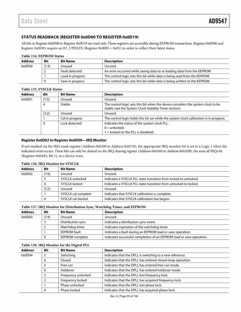
Data Sheet AD9547
STATUS READBACK (REGISTER 0x0D00 TO REGISTER 0x0D19) All bits in Register 0x0D00 to Register 0x0D19 are read only. These registers are accessible during EEPROM transactions. Register 0x0D00 and Register 0x0D01 require an IO_UPDATE (Register 0x0005 = 0x01) in order to reflect their latest status.
Table 134. EEPROM Status Address Bit Bit Name Description 0x0D00 [7:3] Unused Unused.
2 Fault detected An error occurred while saving data to or loading data from the EEPROM. 1 Load in progress The control logic sets this bit while data is being read from the EEPROM. 0 Save in progress The control logic sets this bit while data is being written to the EEPROM.
Table 135. SYSCLK Status Address Bit Bit Name Description 0x0D01 [7:5] Unused Unused.
4 Stable The control logic sets this bit when the device considers the system clock to be stable (see the System Clock Stability Timer section).
[3:2] Unused Unused. 1 Cal in progress The control logic holds this bit set while the system clock calibration is in progress. 0 Lock detected Indicates the status of the system clock PLL.
0 = unlocked. 1 = locked (or the PLL is disabled).
Register 0x0D02 to Register 0x0D09—IRQ Monitor
If not masked via the IRQ mask register (Address 0x0209 to Address 0x0210), the appropriate IRQ monitor bit is set to a Logic 1 when the indicated event occurs. These bits can only be cleared via the IRQ clearing register (Address 0x0A04 to Address 0x0A0B), the reset all IRQs bit (Register 0x0A03, Bit 1), or a device reset.
Table 136. IRQ Monitor for SYSCLK Address Bit Bit Name Description 0x0D02 [7:6] Unused Unused.
5 SYSCLK unlocked Indicates a SYSCLK PLL state transition from locked to unlocked. 4 SYSCLK locked Indicates a SYSCLK PLL state transition from unlocked to locked. [3:2] Unused Unused. 1 SYSCLK cal complete Indicates that SYSCLK calibration is complete. 0 SYSCLK cal started Indicates that SYSCLK calibration has begun.
Table 137. IRQ Monitor for Distribution Sync, Watchdog Timer, and EEPROM Address Bit Bit Name Description 0x0D03 [7:4] Unused Unused.
3 Distribution sync Indicates a distribution sync event. 2 Watchdog timer Indicates expiration of the watchdog timer. 1 EEPROM fault Indicates a fault during an EEPROM load or save operation. 0 EEPROM complete Indicates successful completion of an EEPROM load or save operation.
Table 138. IRQ Monitor for the Digital PLL Address Bit Bit Name Description 0x0D04 7 Switching Indicates that the DPLL is switching to a new reference.
6 Closed Indicates that the DPLL has entered closed-loop operation. 5 Free run Indicates that the DPLL has entered free-run mode. 4 Holdover Indicates that the DPLL has entered holdover mode. 3 Frequency unlocked Indicates that the DPLL lost frequency lock. 2 Frequency locked Indicates that the DPLL has acquired frequency lock. 1 Phase unlocked Indicates that the DPLL lost phase lock. 0 Phase locked Indicates that the DPLL has acquired phase lock.
Rev. G | Page 95 of 106

AD9547 Data Sheet Table 139. IRQ Monitor for History Update, Frequency Limit, and Phase Slew Limit Address Bit Bit Name Description 0x0D05 [7:5] Unused Unused.
4 History updated Indicates the occurrence of a tuning word history update. 3 Frequency unclamped Indicates a frequency limiter state transition from clamped to unclamped. 2 Frequency clamped Indicates a frequency limiter state transition from unclamped to clamped. 1 Phase slew unlimited Indicates a phase slew limiter state transition from slew limiting to not slew limiting. 0 Phase slew limited Indicates a phase slew limiter state transition from not slew limiting to slew limiting.
Table 140. IRQ Monitor for Reference Inputs Address Bit Bit Name Description 0x0D06 7 Ref AA new profile Indicates that Ref AA has switched to a new profile.
6 Ref AA validated Indicates that Ref AA has been validated. 5 Ref AA fault cleared Indicates that Ref AA has been cleared of a previous fault. 4 Ref AA fault Indicates that Ref AA has been faulted. 3 Ref A new profile Indicates that Ref A has switched to a new profile. 2 Ref A validated Indicates that Ref A has been validated. 1 Ref A fault cleared Indicates that Ref A has been cleared of a previous fault. 0 Ref A fault Indicates that Ref A has been faulted.
0x0D07 7 Ref BB new profile Indicates that Ref BB has switched to a new profile. 6 Ref BB validated Indicates that Ref BB has been validated. 5 Ref BB fault cleared Indicates that Ref BB has been cleared of a previous fault. 4 Ref BB fault Indicates that Ref BB has been faulted. 3 Ref B new profile Indicates that Ref B has switched to a new profile. 2 Ref B validated Indicates that Ref B has been validated. 1 Ref B fault cleared Indicates that Ref B has been cleared of a previous fault. 0 Ref B fault Indicates that Ref B has been faulted.
0x0D08 [7:0] Unused Unused. 0x0D09 [7:0]
Table 141. DPLL Status Address Bit Bit Name Description 0x0D0A 7 Offset slew limiting The current closed-loop phase offset is rate limited.
6 Phase build-out A phase build-out transition was made to the currently active reference. 5 Frequency lock The DPLL has achieved frequency lock. 4 Phase lock The DPLL has achieved phase lock. 3 Loop switching The DPLL is in the process of a reference switchover. 2 Holdover The DPLL is in holdover mode. 1 Active The DPLL is active (that is, operating in a closed-loop condition). 0 Free running The DPLL is free running (that is, operating in an open-loop condition).
0x0D0B 7 Frequency clamped The upper or lower frequency tuning word clamp is in effect. 6 History available There is sufficient tuning word history available for holdover operation. [5:3] Active reference priority Priority value of the currently active reference.
000 = highest priority. 111 = lowest priority.
2 Unused Unused. [1:0] Active reference Index of the currently active reference.
00 = Reference A. 01 = Reference AA. 10 = Reference B. 11 = Reference BB.
Rev. G | Page 96 of 106

Data Sheet AD9547
Table 142. Input Reference Status Address Bit Bit Name Description 0x0D0C 7 Profile selected The control logic sets this bit when it assigns Ref A to one of the eight profiles.
[6:4] Selected profile The index (0 to 7) of the profile assigned to Ref A. Note that these bits are meaningless unless Bit 7 = 1.
3 Valid Ref A is valid for use (that is, it is unfaulted, and its validation timer has expired). 2 Fault Ref A is not valid for use. 1 Fast If Bit 7 = 1, this bit indicates that the frequency of Ref A is higher than allowed by its profile settings.
If Bit 7 = 0, this bit indicates that the frequency of Ref A is above the maximum input reference frequency supported by the device.
0 Slow If Bit 7 = 1, this bit indicates that the frequency of Ref A is lower than allowed by its profile settings. If Bit 7 = 0, this bit indicates that the frequency of Ref A is below the minimum input reference frequency supported by the device.
0x0D0D [7:0] Same as 0x0D0C but for REF AA instead of REF A. 0x0D0E [7:0] Same as 0x0D0C but for REF B instead of REF A. 0x0D0F [7:0] Same as 0x0D0C but for REF BB instead of REF A. 0x0D10 [7:0] Unused Unused. 0x0D11 [7:0] 0x0D12 [7:0] 0x0D13 [7:0]
Table 143. Holdover History1 Address Bit Bit Name Description 0x0D14 [7:0] Tuning word
history Tuning word readback, Bits[7:0].
0x0D15 [7:0] Tuning word readback, Bits[15:8]. 0x0D16 [7:0] Tuning word readback, Bits[23:16]. 0x0D17 [7:0] Tuning word readback, Bits[31:24]. 0x0D18 [7:0] Tuning word readback, Bits[39:32]. 0x0D19 [7:0] Tuning word readback, Bits[47:40].
1 These registers contain the current 48-bit DDS frequency tuning word generated by the tuning word history logic.
NONVOLATILE MEMORY (EEPROM) CONTROL (REGISTER 0x0E00 TO REGISTER 0x0E03)
Table 144. Write Protect Address Bit Bit Name Description 0x0E00 [7:2] Unused Unused.
1 Half rate mode EEPROM serial communication rate. 0 (default) = 400 kHz (normal). 1 = 200 kHz.
0 Write enable EEPROM write enable/protect. 0 (default) = EEPROM is write protected. 1 = EEPROM is write enabled.
Table 145. Condition Address Bit Bit Name Description 0x0E01 [7:5] Unused Unused.
[4:0] Condition value When set to a nonzero value (default = 0), these bits establish the condition for EEPROM downloads.
Rev. G | Page 97 of 106

AD9547 Data Sheet Table 146. Save Address Bit Bit Name Description 0x0E02 [7:1] Unused Unused.
0 Save to EEPROM Upload data to the EEPROM based on in the EEPROM storage sequence. This is an autoclearing bit. When an EEPROM save/load transfer is complete, wait a minimum of 10 µs before starting the next EEPROM save/load transfer.
Table 147. Load Address Bit Bit Name Description 0x0E03 [7:2] Unused Unused.
1 Load from EEPROM
Download data from the EEPROM. This is an autoclearing bit. When an EEPROM save/load transfer is complete, wait a minimum of 10 µs before starting the next EEPROM save/load transfer.
0 Unused Unused.
EEPROM STORAGE SEQUENCE (REGISTER 0x0E10 TO REGISTER 0x0E3F) The default settings of Register 0x0E10 to Register 0x0E33 embody a sample scratch pad instruction sequence. The following is a description of the register defaults under the assumption that the controller has been instructed to carry out an EEPROM storage sequence.
Table 148. EEPROM Storage Sequence for System Clock Settings Address Bit Bit Name Description 0x0E10 [7:0] System clock The default value of this register is 0x08, which the controller interprets as a data instruction. Its
decimal value is 8, which tells the controller to transfer nine bytes of data (8 + 1) beginning at the address specified by the next two bytes. The controller stores 0x08 in the EEPROM and increments the EEPROM address pointer.
0x0E11 [7:0] System clock The default value of these two registers is 0x0100. Note that Register 0x0E11 and Register 0x0E12 are the most significant and least significant bytes of the target address, respectively. Because the previous register contains a data instruction, these two registers define a starting address (in this case, 0x0100). The controller stores 0x0100 in the EEPROM and increments the EEPROM pointer by 2. It then transfers nine bytes from the register map (beginning at Address 0x0100) to the EEPROM and increments the EEPROM address pointer by 10 (nine data bytes and one checksum byte). The nine bytes transferred correspond to the system clock parameters in the register map.
0x0E12 [7:0]
0x0E13 [7:0] I/O update The default value of this register is 0x80, which the controller interprets as an I/O update instruction. The controller stores 0x80 in the EEPROM and increments the EEPROM address pointer.
Table 149. EEPROM Storage Sequence for System Clock Calibration Address Bit Bit Name Description 0x0E14 [7:0] SYSCLK calibrate The default value of this register is 0xA0, which the controller interprets as a calibrate instruction.
The controller stores 0xA0 in the EEPROM and increments the EEPROM address pointer.
Table 150. EEPROM Storage Sequence for General Configuration Settings Address Bit Bit Name Description 0x0E15 [7:0] General The default value of this register is 0x14, which the controller interprets as a data instruction. Its
decimal value is 20, which tells the controller to transfer 21 bytes of data (20 + 1) beginning at the address specified by the next two bytes. The controller stores 0x14 in the EEPROM and increments the EEPROM address pointer.
0x0E16 [7:0] General The default value of these two registers is 0x0200. Note that Register 0x0E16 and Register 0x0E17 are the most significant and least significant bytes of the target address, respectively. Because the previous register contains a data instruction, these two registers define a starting address (in this case, 0x0200). The controller stores 0x0200 in the EEPROM and increments the EEPROM pointer by 2. It then transfers 21 bytes from the register map (beginning at Address 0x0200) to the EEPROM and incre-ments the EEPROM address pointer by 22 (21 data bytes and one checksum byte). The 21 bytes transferred correspond to the general configuration parameters in the register map.
0x0E17 [7:0]
Rev. G | Page 98 of 106

Data Sheet AD9547
Table 151. EEPROM Storage Sequence for DPLL Settings Address Bit Bit Name Description 0x0E18 [7:0] DPLL The default value of this register is 0x1B, which the controller interprets as a data instruction. Its
decimal value is 27, which tells the controller to transfer 28 bytes of data (27 + 1) beginning at the address specified by the next two bytes. The controller stores 0x1B in the EEPROM and increments the EEPROM address pointer.
0x0E19 [7:0] DPLL The default value of these two registers is 0x0300. Note that Register 0x0E19 and Register 0x0E1A are the most significant and least significant bytes of the target address, respectively. Because the previous register contains a data instruction, these two registers define a starting address (in this case, 0x0300). The controller stores 0x0300 in the EEPROM and increments the EEPROM pointer by 2. It then transfers 28 bytes from the register map (beginning at Address 0x0300) to the EEPROM and increments the EEPROM address pointer by 29 (28 data bytes and one checksum byte). The 28 bytes transferred correspond to the DPLL parameters in the register map.
0x0E1A [7:0]
Table 152. EEPROM Storage Sequence for Clock Distribution Settings Address Bit Bit Name Description 0x0E1B [7:0] Clock distribution The default value of this register is 0x19, which the controller interprets as a data instruction. Its
decimal value is 25; this tells the controller to transfer 26 bytes of data (25 + 1) beginning at the address specified by the next two bytes. The controller stores 0x19 in the EEPROM and increments the EEPROM address pointer.
0x0E1C [7:0] Clock distribution The default value of these two registers is 0x0400. Note that Register 0x0E1C and Register 0x0E1D are the most significant and least significant bytes of the target address, respectively. Because the previous register contains a data instruction, these two registers define a starting address (in this case, 0x0400). The controller stores 0x0400 in the EEPROM and increments the EEPROM pointer by 2. It then transfers 26 bytes from the register map (beginning at Address 0x0400) to the EEPROM and increments the EEPROM address pointer by 27 (26 data bytes and one checksum byte). The 26 bytes transferred correspond to the clock distribution parameters in the register map.
0x0E1D [7:0]
0x0E1E [7:0] I/O update The default value of this register is 0x80, which the controller interprets as an I/O update instruction. The controller stores 0x80 in the EEPROM and increments the EEPROM address pointer.
Table 153. EEPROM Storage Sequence for Reference Input Settings Address Bit Bit Name Description 0x0E1F [7:0] Reference inputs The default value of this register is 0x07, which the controller interprets as a data instruction. Its
decimal value is 7, which tells the controller to transfer eight bytes of data (7 + 1), beginning at the address specified by the next two bytes. The controller stores 0x07 in the EEPROM and increments the EEPROM address pointer.
0x0E20 [7:0] Reference inputs The default value of these two registers is 0x0500. Note that Register 0x0E20 and Register 0x0E21 are the most significant and least significant bytes of the target address, respectively. Because the previous register contains a data instruction, these two registers define a starting address (in this case, 0x0500). The controller stores 0x0500 in the EEPROM and increments the EEPROM pointer by 2. It then transfers eight bytes from the register map (beginning at Address 0x0500) to the EEPROM and increments the EEPROM address pointer by nine (eight data bytes and one checksum byte). The eight bytes transferred correspond to the reference inputs parameters in the register map.
0x0E21 [7:0]
Table 154. EEPROM Storage Sequence for Profile 0 and Profile 1 Settings Address Bit Bit Name Description 0x0E22 [7:0] Profile 0 and Profile 1 The default value of this register is 0x63, which the controller interprets as a data instruction. Its
decimal value is 99, which tells the controller to transfer 100 bytes of data (99 + 1), beginning at the address specified by the next two bytes. The controller stores 0x63 in the EEPROM and increments the EEPROM address pointer.
0x0E23 [7:0] Profile 0 and Profile 1 The default value of these two registers is 0x0600. Note that Register 0x0E23 and Register 0x0E24 are the most significant and least significant bytes of the target address, respectively. Because the previous register contains a data instruction, these two registers define a starting address (in this case, 0x0600). The controller stores 0x0600 in the EEPROM and increments the EEPROM pointer by 2. It then transfers 100 bytes from the register map (beginning at Address 0x0600) to the EEPROM and increments the EEPROM address pointer by 101 (100 data bytes and one checksum byte). The 99 bytes transferred correspond to the Profile 0 and Profile 1 parameters in the register map.
0x0E24 [7:0]
Rev. G | Page 99 of 106

AD9547 Data Sheet Table 155. EEPROM Storage Sequence for Profile 2 and Profile 3 Settings Address Bit Bit Name Description 0x0E25 [7:0] Profile 2 and Profile 3 The default value of this register is 0x63, which the controller interprets as a data instruction. Its
decimal value is 99, which tells the controller to transfer 100 bytes of data (99 + 1), beginning at the address specified by the next two bytes. The controller stores 0x63 in the EEPROM and increments the EEPROM address pointer.
0x0E26 [7:0] Profile 2 and Profile 3 The default value of these two registers is 0x0680. Note that Register (0x0E26 and Register 0x0E27 are the most significant and least significant bytes of the target address, respectively. Because the previous register contains a data instruction, these two registers define a starting address (in this case, 0x0680). The controller stores 0x0680 in the EEPROM and increments the EEPROM pointer by 2. It then transfers 100 bytes from the register map (beginning at Address 0x0680) to the EEPROM and increments the EEPROM address pointer by 101 (100 data bytes and one checksum byte). The 99 bytes transferred correspond to the Profile 2 and Profile 3 parameters in the register map.
0x0E27 [7:0]
Table 156. EEPROM Storage Sequence for Profile 4 and Profile 5 Settings Address Bit Bit Name Description 0x0E28 [7:0] Profile 4 and Profile 5 The default value of this register is 0x63, which the controller interprets as a data instruction.
Its decimal value is 99, which tells the controller to transfer 100 bytes of data (99 + 1) beginning at the address specified by the next two bytes. The controller stores 0x63 in the EEPROM and increments the EEPROM address pointer.
0x0E29 [7:0] Profile 4 and Profile 5 The default value of these two registers is 0x0700. Note that Register 0x0E29 and Register 0x0E2A are the most significant and least significant bytes of the target address, respectively. Because the previous register contains a data instruction, these two registers define a starting address (in this case, 0x0700). The controller stores 0x0700 in the EEPROM and increments the EEPROM pointer by 2. It then transfers 100 bytes from the register map (beginning at Address 0x0700) to the EEPROM and increments the EEPROM address pointer by 101 (100 data bytes and one checksum byte). The 99 bytes transferred correspond to the Profile 4 and Profile 5 parameters in the register map.
0x0E2A [7:0]
Table 157. EEPROM Storage Sequence for Profile 6 and Profile 7 Settings Address Bit Bit Name Description 0x0E2B [7:0] Profile 6 and Profile 7 The default value of this register is 0x63, which the controller interprets as a data instruction.
Its decimal value is 99, this tells the controller to transfer 100 bytes of data (99 + 1) beginning at the address specified by the next two bytes. The controller stores 0x63 in the EEPROM and increments the EEPROM address pointer.
0x0E2C [7:0] Profile 6 and Profile 7 The default value of these two registers is 0x0780. Note that Register 0x0E2C and Register 0x0E2D are the most significant and least significant bytes of the target address, respectively. Because the previous register contains a data instruction, these two registers define a starting address (in this case, 0x0780). The controller stores 0x0780 in the EEPROM and increments the EEPROM pointer by 2. It then transfers 100 bytes from the register map (beginning at Address 0x0780) to the EEPROM and increments the EEPROM address pointer by 101 (100 data bytes and one checksum byte). The 99 bytes transferred correspond to the Profile 6 and Profile 7 parameters in the register map.
0x0E2D [7:0]
0x0E2E [7:0] I/O update The default value of this register is 0x80, which the controller interprets as an I/O update instruction. The controller stores 0x80 in the EEPROM and increments the EEPROM address pointer.
Rev. G | Page 100 of 106
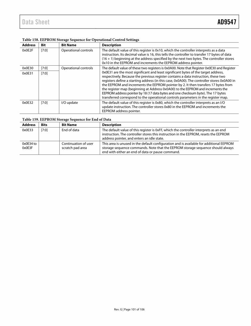
Data Sheet AD9547
Table 158. EEPROM Storage Sequence for Operational Control Settings Address Bit Bit Name Description 0x0E2F [7:0] Operational controls The default value of this register is 0x10, which the controller interprets as a data
instruction. Its decimal value is 16, this tells the controller to transfer 17 bytes of data (16 + 1) beginning at the address specified by the next two bytes. The controller stores 0x10 in the EEPROM and increments the EEPROM address pointer.
0x0E30 [7:0] Operational controls The default value of these two registers is 0x0A00. Note that Register 0x0E30 and Register 0x0E31 are the most significant and least significant bytes of the target address, respectively. Because the previous register contains a data instruction, these two registers define a starting address (in this case, 0x0A00). The controller stores 0x0A00 in the EEPROM and increments the EEPROM pointer by 2. It then transfers 17 bytes from the register map (beginning at Address 0x0A00) to the EEPROM and increments the EEPROM address pointer by 18 (17 data bytes and one checksum byte). The 17 bytes transferred correspond to the operational controls parameters in the register map.
0x0E31 [7:0]
0x0E32 [7:0] I/O update The default value of this register is 0x80, which the controller interprets as an I/O update instruction. The controller stores 0x80 in the EEPROM and increments the EEPROM address pointer.
Table 159. EEPROM Storage Sequence for End of Data Address Bits Bit Name Description 0x0E33 [7:0] End of data The default value of this register is 0xFF, which the controller interprets as an end
instruction. The controller stores this instruction in the EEPROM, resets the EEPROM address pointer, and enters an idle state.
0x0E34 to 0x0E3F
Continuation of user scratch pad area
This area is unused in the default configuration and is available for additional EEPROM storage sequence commands. Note that the EEPROM storage sequence should always end with either an end of data or pause command.
Rev. G | Page 101 of 106

AD9547 Data Sheet
Rev. G | Page 102 of 106
APPLICATIONS INFORMATION POWER SUPPLY PARTITIONS The AD9547 features multiple power supplies, and their power consumption varies with the AD9547 configuration. This section provides information about which power supplies can be grouped together and how the power consumption of each block varies with frequency.
The numbers quoted in this section are for comparison only. Refer to the Specifications section for exact numbers. With each group, bypass capacitors of 1 μF in parallel with 10 μF should be used.
Upon applying power to the device, internal circuitry monitors the 1.8 V digital core supply and the 3.3 V digital I/O supply. When these supplies cross the desired threshold level, the device generates an internal 10 μs reset pulse. This pulse does not appear on the RESET pin.
3.3 V Supplies
The 3.3 V supply domain consists of two main partitions: digital (DVDD3) and analog (AVDD3). These two supply domains must be kept separate.
Furthermore, the AVDD3 consists of two subdomains: the clock distribution output domain (Pin 25, Pin 31) and the rest of the AVDD3 supply connections. Generally, the AVDD3 supply domains can be joined together. However, if an application requires 1.8 V CMOS driver operation in the clock distribution output block, provide one 1.8 V supply domain to power the clock distribution output block. Each output driver has a dedicated supply pin, as shown in Table 160.
Table 160. Output Driver Supply Pins
Output Driver Supply Pin OUT0 25 OUT1 31
1.8 V Supplies
The 1.8 V supply domain consists of two main partitions: digital (DVDD) and analog (AVDD). These two supply domains must be kept separate.
THERMAL PERFORMANCE The AD9547 is specified for a case temperature (TCASE). To ensure that TCASE is not exceeded, an airflow source can be used. Use the following equation to determine the junction temperature on the application PCB:
TJ = TCASE + (ΨJT × PD)
where: TJ is the junction temperature in degrees Celsius (°C). TCASE is the case temperature in degrees Celsius (°C) measured by the customer at the top center of the package. ΨJT is the value that is indicated in Table 161. PD is the power dissipation (see the Power Dissipation section).
Values of θJA are provided for package comparison and PCB design considerations. θJA can be used for a first-order approximation of TJ using the following equation:
TJ = TA + (θJA × PD)
where TA is the ambient temperature in degrees Celsius (°C).
Values of θJC are provided for package comparison and PCB design considerations when an external heat sink is required.
Values of θJB are provided for package comparison and PCB design considerations.
Table 161. Thermal Parameters for the AD9547 64-Lead LFCSP Package Symbol Thermal Characteristic Using a JEDEC51-7 Plus JEDEC51-5 2S2P Test Board1 Value2 Unit θJA Junction-to-ambient thermal resistance, 0.0 m/sec air flow per JEDEC JESD51-2 (still air) 21.7 °C/W θJMA Junction-to-ambient thermal resistance, 1.0 m/sec air flow per JEDEC JESD51-6 (moving air) 18.9 °C/W θJMA Junction-to-ambient thermal resistance, 2.5 m/sec air flow per JEDEC JESD51-6 (moving air) 16.9 °C/W θJB Junction-to-board thermal resistance, per JEDEC JESD51-8 (still air) 11.3 °C/W θJC Junction-to-case thermal resistance 1.2 °C/W ΨJT Junction-to-top-of-package characterization parameter, 0 m/sec airflow per JEDEC JESD51-2 (still air) 0.1 °C/W 1 The exposed pad on the bottom of the package must be soldered to ground to achieve the specified thermal performance. 2 Results are from simulations. The PCB is a JEDEC multilayer type. Thermal performance for actual applications requires careful inspection of the conditions in the
application to determine whether they are similar to those assumed in these calculations.

Data Sheet AD9547
Rev. G | Page 103 of 106
CALCULATING THE DIGITAL FILTER COEFFICIENTS The digital loop filter coefficients (α, β, γ, and δ, as shown in Figure 40) relate to the time constants (T1, T2, and T3) that are associated with the equivalent analog circuit for a third-order loop filter (see Figure 67). Note that AD9547 evaluation software contains a profile designer that will compute these coefficients for you.
R2
FROMCHARGE
PUMPTOVCOR3
C3C1
C2
0830
0-04
2
Figure 67. Third-Order Analog Loop Filter
The design process begins by deciding on two design parameters related to the second-order loop filter shown in Figure 68: the desired open-loop bandwidth (fP) and the phase margin (θ).
R2
FROMCHARGE
PUMPTOVCO
C1
C2
0830
0-04
3
Figure 68. Second-Order Analog Loop Filter
An analysis of the second-order loop filter leads to its primary time constant, T1. It can be shown that T1 is expressible in terms of fP and θ as
)cos()sin(1
P
1 ωT
where ωp = 2πfP
An analysis of the third-order loop filter leads to the definition of another time constant, T3. It can be shown that T3 is expressible in terms of the desired amount of additional attenuation intro-duced by R3 and C3 at some specified frequency offset (fOFFSET) from the PLL output frequency.
OFFSET
ATTEN
3 ωT 110 10
where ωOFFSET = 2πfOFFSET
Note that ATTEN is the desired excess attenuation in decibels (dB). Furthermore, ATTEN and ωOFFSET should be chosen so that
P3 f
T5
1
With an expression for T1 and T3, it is possible to define an adjusted open-loop bandwidth (fC) that is slightly less than fP. It can be shown that ωC (fC expressed as a radian frequency) is expressible in terms of T1, T3, and θ (phase margin) as follows:
1
)tan(1
)tan(2
2
231
3131
3131
31C TT
TTTTTTTT
TTω
It can also be shown that the adjusted open-loop bandwidth leads to T2 (the secondary time constant of the second-order loop filter), which is expressed as
31C2 TTω
T
2
1
Calculation of the digital loop filter coefficients requires a scaling constant, K (related to the system clock frequency, fS), and the PLL feedback divide ratio, D.
SfK 332125,578,517,30
1V
USD
where S, U, and V are the integer and fractional feedback divider values that reside in the profile registers.
Keep in mind that the desired integer feedback divide ratio is one more than the stored value of S (hence, the +1 term in the equation for D in this equation). This leads to the digital filter coefficients given by
2
22
111
2C
3C1C
1
22
C
TωTωTω
KTDTω
α
21S TTfβ
1132
1STfγ 32
3STfδ
32
Calculation of the coefficient register values requires the appli-cation of some special functions, which are described as follows:
The if() function
y = if (test_statement, true_value, false_value)
where: test_statement is a conditional expression (for example, x < 3). true_value is what y equals if the conditional expression is true. false_value is what y equals if the conditional expression is false.
The round() function
y = round(x)
If x is an integer, then y = x. Otherwise, y is the nearest integer to x. For example, round(2.1) = 2, round(2.5) = 3, and round(−3.1) = −3.
The ceil() function
y = ceil(x)
If x is an integer, then y = x. Otherwise, y is the next integer to the right on the number line. For example, ceil(2.8) = 3, whereas ceil(−2.8) = −2.
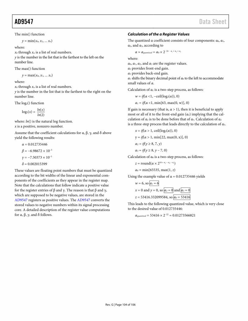
AD9547 Data Sheet The min() function
y = min(x0, x1, ... xn)
where: x0 through xn is a list of real numbers. y is the number in the list that is the farthest to the left on the number line.
The max() function
y = max(x0, x1, ... xn)
where: x0 through xn is a list of real numbers. y is the number in the list that is the farthest to the right on the number line.
The log2() function
log2(x) = )2()(
lnxln
where: ln() is the natural log function. x is a positive, nonzero number.
Assume that the coefficient calculations for α, β, γ, and δ above yield the following results:
α = 0.012735446
β = −6.98672 × 10⁻⁵
γ = −7.50373 × 10⁻⁵
δ = 0.002015399
These values are floating point numbers that must be quantized according to the bit widths of the linear and exponential com-ponents of the coefficients as they appear in the register map. Note that the calculations that follow indicate a positive value for the register entries of β and γ. The reason is that β and γ, which are supposed to be negative values, are stored in the AD9547 registers as positive values. The AD9547 converts the stored values to negative numbers within its signal processing core. A detailed description of the register value computations for α, β, γ, and δ follows.
Calculation of the α Register Values
The quantized α coefficient consists of four components: α0, α1, α2, and α3, according to
α ≈ αquantized = α0 × 2−16 − α1 + α2 + α3
where: α0, α1, α2, and α3 are the register values. α2 provides front-end gain. α3 provides back-end gain. α1 shifts the binary decimal point of α0 to the left to accommodate small values of α.
Calculation of α1 is a two-step process, as follows:
w = if(α <1, −ceil(log2(α)), 0)
α1 = if(α <1, min[63, max(0, w)], 0)
If gain is necessary (that is, α > 1), then it is beneficial to apply most or all of it to the front-end gain (α2) implying that the cal-culation of α2 is to be done before that of α3. Calculation of α2 is a three-step process that leads directly to the calculation of α3.
x = if(α > 1, ceil(log2(α)), 0)
y = if(α > 1, min[22, max(0, x)], 0)
α2 = if(y ≥ 8, 7, y)
α3 = if(y ≥ 8, y – 7, 0)
Calculation of α0 is a two-step process, as follows:
z = round(α × 216 + α1 − α2 − α3)
α0 = min[65535, max(1, z)
Using the example value of α = 0.012735446 yields
w = 6, so α1 = 6
x = 0 and y = 0, so α2 = 0 and α3 = 0
z = 53416.332099584, so α0 = 53416
This leads to the following quantized value, which is very close to the desired value of 0.012735446:
αquantized = 53416 × 2−22 ≈ 0.01273566821
Rev. G | Page 104 of 106
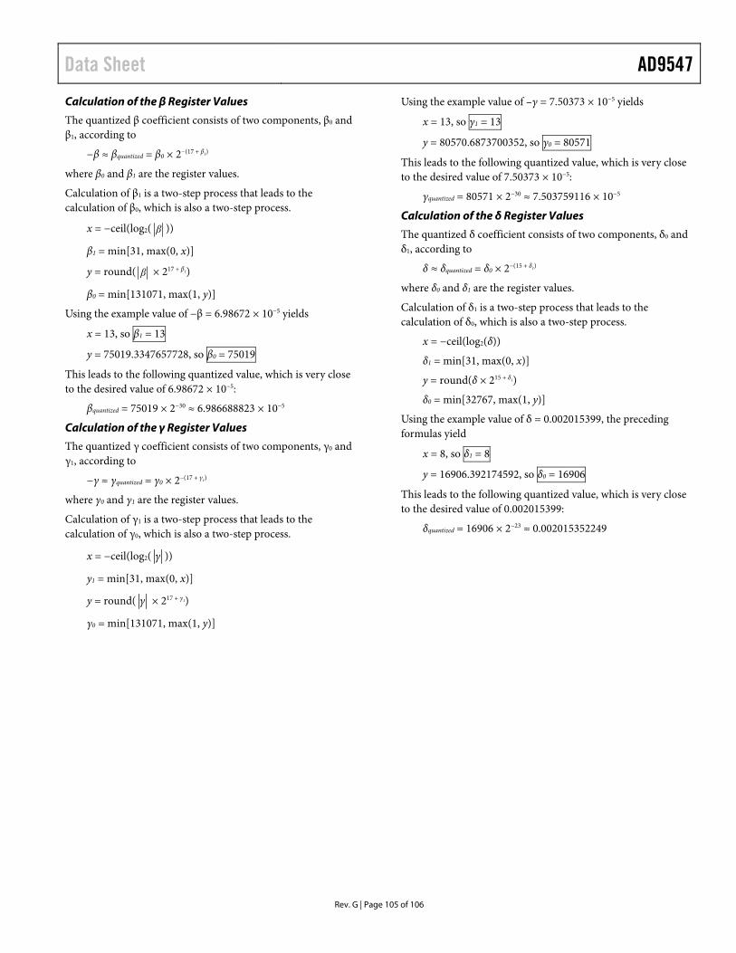
Data Sheet AD9547 Calculation of the β Register Values
The quantized β coefficient consists of two components, β0 and β1, according to
−β ≈ βquantized = β0 × 2−(17 + β1)
where β0 and β1 are the register values.
Calculation of β1 is a two-step process that leads to the calculation of β0, which is also a two-step process.
x = −ceil(log2( β ))
β1 = min[31, max(0, x)]
y = round( β × 217 + β1)
β0 = min[131071, max(1, y)]
Using the example value of −β = 6.98672 × 10⁻⁵ yields
x = 13, so β1 = 13
y = 75019.3347657728, so β0 = 75019
This leads to the following quantized value, which is very close to the desired value of 6.98672 × 10⁻⁵:
βquantized = 75019 × 2−30 ≈ 6.986688823 × 10⁻⁵
Calculation of the γ Register Values
The quantized γ coefficient consists of two components, γ0 and γ1, according to
−γ ≈ γquantized = γ0 × 2−(17 + γ1)
where γ0 and γ1 are the register values.
Calculation of γ1 is a two-step process that leads to the calculation of γ0, which is also a two-step process.
x = −ceil(log2( γ ))
y1 = min[31, max(0, x)]
y = round( γ × 217 + γ1)
γ0 = min[131071, max(1, y)]
Using the example value of –γ = 7.50373 × 10⁻⁵ yields
x = 13, so γ1 = 13
y = 80570.6873700352, so γ0 = 80571
This leads to the following quantized value, which is very close to the desired value of 7.50373 × 10⁻⁵:
γquantized = 80571 × 2−30 ≈ 7.503759116 × 10⁻⁵
Calculation of the δ Register Values
The quantized δ coefficient consists of two components, δ0 and δ1, according to
δ ≈ δquantized = δ0 × 2−(15 + δ1)
where δ0 and δ1 are the register values.
Calculation of δ1 is a two-step process that leads to the calculation of δ0, which is also a two-step process.
x = −ceil(log2(δ))
δ1 = min[31, max(0, x)]
y = round(δ × 215 + δ1)
δ0 = min[32767, max(1, y)]
Using the example value of δ = 0.002015399, the preceding formulas yield
x = 8, so δ1 = 8
y = 16906.392174592, so δ0 = 16906
This leads to the following quantized value, which is very close to the desired value of 0.002015399:
δquantized = 16906 × 2−23 ≈ 0.002015352249
Rev. G | Page 105 of 106
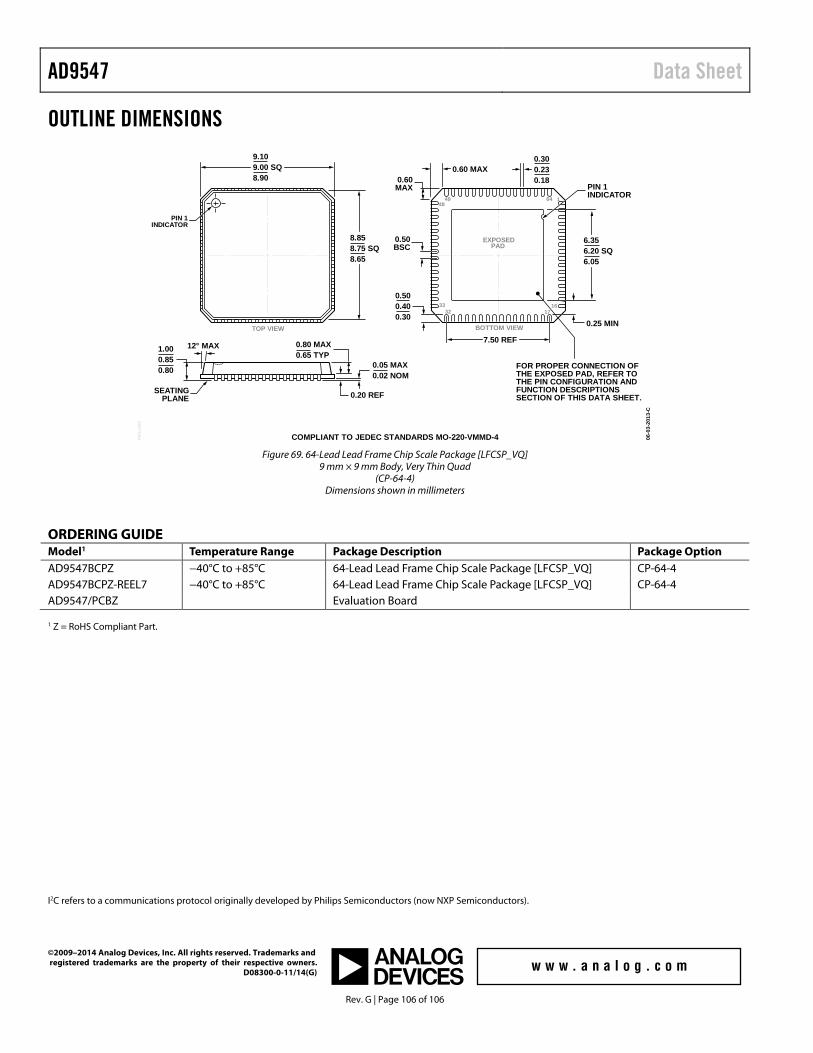
AD9547 Data Sheet
OUTLINE DIMENSIONS
COMPLIANT TO JEDEC STANDARDS MO-220-VMMD-4
0.25 MIN
164
1617
4948
3233
0.500.400.30
0.50BSC
0.20 REF
12° MAX 0.80 MAX0.65 TYP
1.000.850.80
7.50 REF
0.05 MAX0.02 NOM
0.60 MAX0.60MAX
SEATINGPLANE
PIN 1INDICATOR
6.356.20 SQ6.05
PIN 1INDICATOR
0.300.230.18
FOR PROPER CONNECTION OFTHE EXPOSED PAD, REFER TOTHE PIN CONFIGURATION ANDFUNCTION DESCRIPTIONSSECTION OF THIS DATA SHEET.
TOP VIEW
EXPOSEDPAD
BOTTOM VIEW
9.109.00 SQ8.90
8.858.75 SQ8.65
06-0
3-20
13-C
PKG
-118
4
Figure 69. 64-Lead Lead Frame Chip Scale Package [LFCSP_VQ]
9 mm × 9 mm Body, Very Thin Quad (CP-64-4)
Dimensions shown in millimeters
ORDERING GUIDE Model1 Temperature Range Package Description Package Option AD9547BCPZ −40°C to +85°C 64-Lead Lead Frame Chip Scale Package [LFCSP_VQ] CP-64-4 AD9547BCPZ-REEL7 −40°C to +85°C 64-Lead Lead Frame Chip Scale Package [LFCSP_VQ] CP-64-4 AD9547/PCBZ Evaluation Board
1 Z = RoHS Compliant Part.
I2C refers to a communications protocol originally developed by Philips Semiconductors (now NXP Semiconductors).
©2009–2014 Analog Devices, Inc. All rights reserved. Trademarks and registered trademarks are the property of their respective owners. D08300-0-11/14(G)
Rev. G | Page 106 of 106