dsp sharc processors part1
TRANSCRIPT
8/7/2019 DSP SHARC Processors PART1
http://slidepdf.com/reader/full/dsp-sharc-processors-part1 1/33
1 INTRODUCTION TO SHARCPROCESSORS
This chapter briefly describes the SHARC processor’s architecture and keyfeatures and compares available models.
Topics include:• “What are SHARC Processors?” on page 1-1• “Three Generations of SHARC Processors” on page 1-5
What are SHARC Processors?SHARC is the name of a family of high-performance 32-bit floating-pointprocessors based on a Super Harvard Architecture. SHARC processorsdominate the floating-point digital signal processing market, deliveringexceptional core and memory performance complemented by outstandingI/O throughput. The industry standard SHARC family makes floating-point processing economical for applications where performance anddynamic range are key considerations such as home, professional, andautomotive audio, medical, and industrial and instrumentation products.
The SHARC processor portfolio currently consists of three generations of products providing code-compatible solutions, ranging from entry-levelproducts priced at less than $10 to the highest performance productsoffering fixed- and floating-point computational power to 400 MHz/2400MFLOPs. Regardless of the specific product choice, all SHARC processorsprovide a common set of features and functionality usable across manysignal processing markets and applications. This baseline functionalityenables the SHARC user to leverage legacy code and design experience,while transitioning to higher-performance, more highly integratedSHARC products.By integrating on-chip, single-instruction, multiple-data (SIMD) processingelements, SDRAM, and I/O peripherals, SHARC processors deliverbreakthrough signal processing performance.
SHARC Applications The combination of a high performance core surrounded by appropriateperipherals, a large software library, and award-winning development toolsmakes SHARC processors the ideal choice for audio and broad marketprocessor applications. Here are some applications:
8/7/2019 DSP SHARC Processors PART1
http://slidepdf.com/reader/full/dsp-sharc-processors-part1 2/33
• Home theater/digital home applications. The ADSP-21266,ADSP-21365/6, and ADSP-21367 processors permit highly efficientsoftware implementations of audio decode and post processingalgorithms, such as Dolby Digital, Dolby Digital EX, DTS-ES Discrete6.1, DTS-ESMatrix 6.1, DTS 96/24™ 5.1, MPEG-2 AACLC, MPEG-2 BC 2ch, Dolby Pro Logic II, Dolby Pro Logic 2x,DTS Neo:6, and WMA Pro. Libraries of all standard–and manyproprietary–audio algorithms reside in on-chip ROM, eliminatingthe need for external ROM.• Professional audio applications. A number of the third-generationSHARC processors are well-suited for professional audio applications
requiring high processing power and advanced on-chipperipherals such as sample rate conversion, S/PDIF transmitter/receiver, and BGA and LQFP package options.• Automotive audio applications. The ADSP-2136x, with integrationof sample-rate conversion, DTCP cipher, precision clockgenerators, and serial ports, is an ideal choice for new multichannelautomotive audio designs.• Broad market use. SHARC processors are available in commercial,industrial, and automotive temperature grade packages. They areused in a wide variety of signal processing applications, providingup to 400 MHz performance in a single instruction, multiple data
architecture (SIMD). Applications include imaging, medicaldevices, communications, military, test equipment, 3-D graphics,speech recognition, and motor control.
Architecture Overview This section describes architectural features of the SHARC processor.Super Harvard Architecture
The 32-bit floating-point SHARC processors from Analog Devices arebased on a Super Harvard architecture that balances exceptional coreandmemory performance with outstanding I/O throughput capabilities.
Thisarchitecture extends the original concepts of separate program anddatamemory busses by adding an I/O processor with its associateddedicatedbusses.In addition to satisfying the demands of the most computationallyintensive,

8/7/2019 DSP SHARC Processors PART1
http://slidepdf.com/reader/full/dsp-sharc-processors-part1 3/33
real-time signal processing applications, SHARC processors integratelarge memory arrays and application-specific peripherals designed tosimplifyproduct development and reduce time to market.
Common Architectural FeaturesSHARC processors share the following architectural features.• 32/40-bit IEEE floating-point math• 32-bit fixed-point multipliers with 64-bit product and 80-bitaccumulation• No arithmetic pipeline. All computations are single-cycle.
• Circular buffer addressing supported in hardware• Sixteen address pointers support 16 circular buffers.• Six nested levels of zero-overhead looping in hardware• Rich algebraic assembly language syntax• Conditional arithmetic, bit manipulation, divide and square root,bit field deposit and extract supported by instruction set• Zero-overhead background transfers at full clock rate withoutprocessorinterventionIn the core, every instruction can execute in a single cycle. The busesand
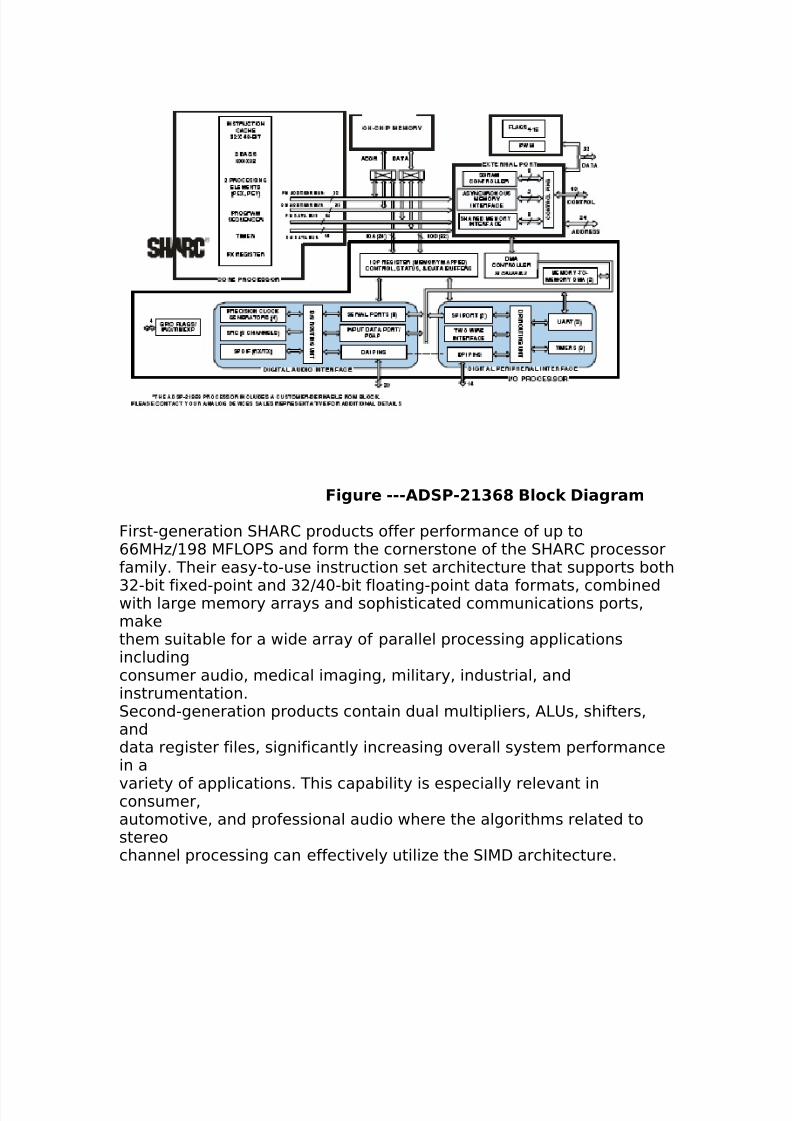
instruction cache provide rapid unimpeded data flow to the core tomaintainthe execution rate.Figure 1-1 on page 1-6 shows a detailed block diagram of a single coreSHARC 32-bit processor and the I/O processor (IOP). It illustrates thefollowing architectural features:• Two processing elements (PEx and PEy), each containing 32-bitIEEE floating-point computation units–multiplier, arithmeticlogic unit (ALU), shifter, and data register file• Program sequencer with related instruction cache, interval timer,and data address generators (DAG1 and DAG2)
• An SDRAM controller that provides an interface to as many as fourseparate banks of industry-standard SDRAM devices• Up to a maximum of 4 Mbits of on-chip SRAM and 6 Mbits of on-chip, mask-programmable ROM• Input/output processor (IOP) with integrated direct memoryaccess (DMA) controller, serial peripheral interface (SPI) compatibleport, and serial ports (SPORTs) for point-to-pointmultiprocessor communications
8/7/2019 DSP SHARC Processors PART1
http://slidepdf.com/reader/full/dsp-sharc-processors-part1 4/33
• A variety of audio-centric peripheral modules including aSony/Philips digital interface (S/PDIF), sample rate converter(SRC), and pulse width modulation (PWM). Table 1-1 onpage 1-6 provides details on these and other features for the currentmembers of the ADSP-2136x processor generation.
• JTAG test access port for emulationFigure 1-1 also shows the three on-chip buses of the ADSP-21367/8/9
processors: the PM bus, DM bus, and I/O bus. The PM bus providesaccess to instructions or data. During a single cycle, these buses lettheprocessor access two data operands from memory, access aninstruction(from cache), and perform a DMA transfer. In addition, Figure 1-1showsthe asychronous memory interface available on the ADSP-21368processor.
Three Generations of SHARC Processors The SHARC architecture has a long history in the floating-pointprocessormarket. While architectural enhancements have been made with eachsuccessive processor generation, the common traits of exceptionalfloating-point performance, matched to high-bandwidth memory and I/Otransfers, remains. All three generations of SHARC processors are stillinproduction, offering a variety of code-compatible options to meet awidearray of price, performance, and footprint requirements.

8/7/2019 DSP SHARC Processors PART1
http://slidepdf.com/reader/full/dsp-sharc-processors-part1 5/33
8/7/2019 DSP SHARC Processors PART1
http://slidepdf.com/reader/full/dsp-sharc-processors-part1 6/33
Figure ---ADSP-21368 Block Diagram
First-generation SHARC products offer performance of up to66MHz/198 MFLOPS and form the cornerstone of the SHARC processorfamily. Their easy-to-use instruction set architecture that supports both
32-bit fixed-point and 32/40-bit floating-point data formats, combinedwith large memory arrays and sophisticated communications ports,makethem suitable for a wide array of parallel processing applicationsincludingconsumer audio, medical imaging, military, industrial, andinstrumentation.Second-generation products contain dual multipliers, ALUs, shifters,anddata register files, significantly increasing overall system performancein a
variety of applications. This capability is especially relevant inconsumer,automotive, and professional audio where the algorithms related tostereochannel processing can effectively utilize the SIMD architecture.

8/7/2019 DSP SHARC Processors PART1
http://slidepdf.com/reader/full/dsp-sharc-processors-part1 7/33
Third-generation SHARC products employ an enhanced SIMDarchitecturethat extends CPU performance to 400 MHz/2400 MFLOPS. Theseproducts also integrate a variety of ROM configurations and audio-centricperipherals designed to decrease time to market and reduce theoverall billof materials costs. This increased level of performance and peripheralintegrationallow third-generation SHARC processors to be considered assingle chip solutions for a variety of audio markets.
Each SHARC processor provides unique capabilities, while beingpin-compatible with other SHARC devices. Table 1-1 on page 1-8 listskey third generation SHARC processor specifications. For moreinformation,view the SHARC processor selection table online at the AnalogDevices Web site at:http://www.analog.com/sharc
Processor Peripherals and PerformanceSHARC processors represent a class of devices that combine anextremely
capable single-instruction, multiple-data (SIMD) processor engine withfeatures like core timers, general purpose timers, UARTs, and SPIports.In addition to advanced peripherals, SHARC processors use a softwareprogrammable, on-chip phase lock loop (PLL) that allows softwarecontrolduring runtime of core and peripheral clock of the SHARC processors.
PerformanceReal-time signal processing tasks are I/O and computationallyintensive.In addition to high-speed math units and single-cycle instructionexecution(including single-cycle multiply accumulates [MACs]), SHARCprocessors are designed for maximum I/O and memory accessbandwidth.
This balance of core speed, memory integration, and I/O bandwidthachieves the sustained performance critical to real-time applications.

8/7/2019 DSP SHARC Processors PART1
http://slidepdf.com/reader/full/dsp-sharc-processors-part1 8/33

8/7/2019 DSP SHARC Processors PART1
http://slidepdf.com/reader/full/dsp-sharc-processors-part1 9/33
ADSP-21262 EZ-KIT Lite Evaluation System
Processor Core The processor core consists of two processing elements (each withthree
computation units and data register file), a program sequencer, twoDAGs, a timer, and an instruction cache. All processing occurs in theprocessorcore.Processing Elements
The processor core contains two processing elements: PEx and PEy.Each
element contains a data register file and three independentcomputationunits: an arithmetic logic unit (ALU), a multiplier with an 80-bitfixed-point accumulator, and a shifter. For meeting a wide variety of processingneeds, the computation units process data in three formats: 32-bitfixed-point, 32-bit floating-point, and 40-bit floating-point. The floating-point operations are single-precision IEEE-compatible. The 32-bitfloating-point format is the standard IEEE format, whereas the 40-bitextended-precision format has eight additional least significant bits(LSBs)of mantissa for greater accuracy.
The ALU performs a set of arithmetic and logic operations on bothfixed-point and floating-point formats. The multiplier performs floating-point or fixed-point multiplication and fixed-pointmultiply/accumulate or multiply/cumulative-subtract operations. Theshifter performs logical and arithmetic shifts, bit manipulation, bit-wisefield deposit and extraction, and exponent derivation operations on 32-bitoperands. These computation units complete all operations in a singlecycle; there is no computation pipeline. The output of any unit mayserveas the input of any unit on the next cycle. All units are connected inparallel,rather than serially. In a multifunction computation, the ALU andmultiplier perform independent, simultaneous operations.

8/7/2019 DSP SHARC Processors PART1
http://slidepdf.com/reader/full/dsp-sharc-processors-part1 10/33
Each processing element has a general-purpose data register file thattransfersdata between the computation units and the data buses and storesintermediate results. A register file has two sets (primary andsecondary) of
16 general-purpose registers each for fast context switching. All of theregistersare 40 bits wide. The register file, combined with the coreprocessor’s Super Harvard Architecture, allows unconstrained data flowbetween computation units and internal memory.Primary processing element (PEx). PEx processes allcomputationalinstructions whether the processor is in single-instruction, single-data(SISD) or single-instruction, multiple-data (SIMD) mode. This elementcorresponds to the computational units and register file in previousADSP-21000 family processors.
Secondary processing element (PEy). PEy processes eachcomputationalinstruction in lock-step with PEx, but only processes these instructionswhen the processor is in SIMD mode. Because many operations areinfluencedby this mode, more information on SIMD is available in multiplelocations:
• For information on PEy operations, see “Processing Elements” onpage 2-1 .• For information on data addressing in SIMD mode, see “Addressingin SISD and SIMD Modes” on page 4-20 .• For information on data accesses in SIMD mode, see “SISD,SIMD, and Broadcast Load Modes” on page 5-37 .
• For information on SIMD programming, see “Instruction Set” inChapter 8, Instruction Set , and “Computations Reference” inChapter 9, Computations Reference .Program Sequence ControlInternal controls for program execution come from four functionalblocks:program sequencer, data address generators, core timer, andinstruction
8/7/2019 DSP SHARC Processors PART1
http://slidepdf.com/reader/full/dsp-sharc-processors-part1 11/33
cache. Two dedicated address generators and a program sequencersupplyaddresses for memory accesses. Together the sequencer and dataaddressgenerators allow computational operations to execute with maximum
efficiency since the computation units can be devoted exclusively toprocessingdata. With its instruction cache, the ADSP-2136x processors cansimultaneously fetch an instruction from the cache and access twodataoperands from memory. The DAGs also provide built-in support forzero-overhead circular buffering.Program sequencer. The program sequencer supplies instructionaddresses to program memory. It controls loop iterations andevaluatesconditional instructions. With an internal loop counter and loop stack,
the processors execute looped code with zero overhead. No explicit jumpinstructions are required to loop or to decrement and test the counter.
Toachieve a high execution rate while maintaining a simple programmingmodel, the processor employs a five stage pipeline to processinstructions— fetch1, fetch2, decode, address and execute. For moreinformation, see“Instruction Pipeline” on page 3-2.Data address generators. The DAGs provide memory addresses
when datais transferred between memory and registers. Dual data addressgeneratorsenable the processor to output simultaneous addresses for twooperandreads or writes. DAG1 supplies 32-bit addresses for accesses using theDMbus. DAG2 supplies 32-bit addresses for memory accesses over the PMbus.Each DAG keeps track of up to eight address pointers, eight addressmodifiers,
and for circular buffering eight base-address registers and eightbuffer-length registers. A pointer used for indirect addressing can bemodified

8/7/2019 DSP SHARC Processors PART1
http://slidepdf.com/reader/full/dsp-sharc-processors-part1 12/33
by a value in a specified register, either before (pre-modify) or after(post-modify) the access. A length value may be associated with each
pointer to perform automatic modulo addressing for circular databuffers. The circular buffers can be located at arbitrary boundaries in memory.Each DAG register has a secondary register that can be activated forfastcontext switching.Circular buffers allow efficient implementation of delay lines and otherdata structures required in digital signal processing They are alsocommonlyused in digital filters and Fourier transforms. The DAGsautomatically handle address pointer wraparound, reducing overhead,
increasing performance, and simplifying implementation.Interrupts. The ADSP-2136x processors have three external hardwareinterrupts. The processor also provides three general-purposeinterrupts,and a special interrupt for reset. The processor has internally-generatedinterrupts for the timer, DMA controller operations, circular bufferoverflow,stack overflows, arithmetic exceptions, and user-defined softwareinterrupts.For the general-purpose interrupts and the internal timer interrupt, the
processor automatically stacks the arithmetic status ( ASTATx ) registerandmode ( MODE1 ) registers in parallel with the interrupt servicing, allowing15nesting levels of very fast service for these interrupts.Context switch. Many of the processor’s registers have secondaryregistersthat can be activated during interrupt servicing for a fast contextswitch.
The data registers in the register file, the DAG registers, and themultiplier
result register all have secondary registers. The primary registers areactiveat reset, while the secondary registers are activated by control bits in amode control register.Timer. The core’s programmable interval timer provides periodicinterruptgeneration. When enabled, the timer decrements a 32-bit countregister every cycle. When this count register reaches zero, the
8/7/2019 DSP SHARC Processors PART1
http://slidepdf.com/reader/full/dsp-sharc-processors-part1 13/33
ADSP-2136x processors generate an interrupt and asserts their timerexpired output. The count register is automatically reloaded from a 32-bitperiod register and the countdown resumes immediately.Instruction cache. The program sequencer includes a 32-word
instructioncache that effectively provides three-bus operation for fetching aninstructionand two data values. The cache is selective; only instructions whosefetches conflict with data accesses using the PM bus are cached. Thiscaching allows full speed execution of core, looped operations such asdigital
filter multiply-accumulates, and FFT butterfly processing. For moreinformation on the cache, refer to “Using the Cache” on page 3-8 .Processor Internal Buses
The processor core has six buses: PM address, PM data, DM address,DMdata, I/O address, and I/O data. The PM bus is used to fetch instructionsfrom memory, but may also be used to fetch data. The DM bus can
onlybe used to fetch data from memory. The I/O bus is used solely by theIOPto facilitate DMA transfers. In conjunction with the cache, this SuperHarvard Architecture allows the core to fetch an instruction and twopieces of data in the same cycle that a data word is moved betweenmemoryand a peripheral. This architecture allows dual data fetches, when theinstruction is supplied by the cache.Bus capacities. The PM and DM address buses are both 32 bits wide,while the PM and DM data buses are both 64 bits wide.
These two buses provide a path for the contents of any register in theprocessorto be transferred to any other register or to any data memorylocation in a single cycle. When fetching data over the PM or DM bus,theaddress comes from one of two sources: an absolute value specified inthe

8/7/2019 DSP SHARC Processors PART1
http://slidepdf.com/reader/full/dsp-sharc-processors-part1 14/33
instruction (direct addressing) or the output of a data addressgenerator(indirect addressing). These two buses share the same port of thememory.Each memory block also has a dedicated I/O address bus and I/O data
busto let the I/O processor access internal memory for DMA withoutdelayingthe processor core (in the absence of memory block conflict). The I/Oaddress bus is 18 bits wide, and the I/O data bus is 32 bits wide.Data transfers. Nearly every register in the processor core isclassified as auniversal register ( Ureg ). Instructions allow the transfer of data betweenany two universal registers or between a universal register andmemory.
This support includes transfers between control registers, status
registers,and data registers in the register file. The PM bus connect ( PX) registerspermit data to be passed between the 64-bit PM data bus and the 64-bitDM data bus, or between the 40-bit register file and the PM data bus.
These registers contain hardware to handle the data width difference.Formore information, see “Processing Element Registers” on page B-22.
A INSTRUCTION SET QUICK REFERENCE
This instruction set summary provides a syntax summary for eachinstructionand includes a cross reference to each instruction’s reference page.

8/7/2019 DSP SHARC Processors PART1
http://slidepdf.com/reader/full/dsp-sharc-processors-part1 15/33
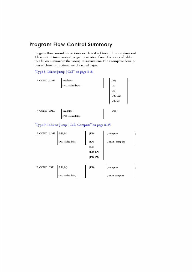
Chapter Overview The following summary topics appear in this chapter.• “Compute and Move/Modify Summary” on page A-2• “Program Flow Control Summary” on page A-4• “Immediate Move Summary” on page A-5• “Miscellaneous Operations Summary” on page A-7• “Register Types Summary” on page A-9• “Memory Addressing Summary” on page A-13• “Instruction Set Notation Summary” on page A-14• “Conditional Execution Codes Summary” on page A-16• “SISD/SIMD Conditional Testing Summary” on page A-18• “Instruction Opcode Acronym Summary” on page A-19• “Universal Register Codes” on page A-23• “ADSP-2136x Instruction Opcode Map” on page A-28

8/7/2019 DSP SHARC Processors PART1
http://slidepdf.com/reader/full/dsp-sharc-processors-part1 16/33

8/7/2019 DSP SHARC Processors PART1
http://slidepdf.com/reader/full/dsp-sharc-processors-part1 17/33
8/7/2019 DSP SHARC Processors PART1
http://slidepdf.com/reader/full/dsp-sharc-processors-part1 18/33

8/7/2019 DSP SHARC Processors PART1
http://slidepdf.com/reader/full/dsp-sharc-processors-part1 19/33

8/7/2019 DSP SHARC Processors PART1
http://slidepdf.com/reader/full/dsp-sharc-processors-part1 20/33

8/7/2019 DSP SHARC Processors PART1
http://slidepdf.com/reader/full/dsp-sharc-processors-part1 21/33

8/7/2019 DSP SHARC Processors PART1
http://slidepdf.com/reader/full/dsp-sharc-processors-part1 22/33

8/7/2019 DSP SHARC Processors PART1
http://slidepdf.com/reader/full/dsp-sharc-processors-part1 23/33

8/7/2019 DSP SHARC Processors PART1
http://slidepdf.com/reader/full/dsp-sharc-processors-part1 24/33

8/7/2019 DSP SHARC Processors PART1
http://slidepdf.com/reader/full/dsp-sharc-processors-part1 25/33

8/7/2019 DSP SHARC Processors PART1
http://slidepdf.com/reader/full/dsp-sharc-processors-part1 26/33

8/7/2019 DSP SHARC Processors PART1
http://slidepdf.com/reader/full/dsp-sharc-processors-part1 27/33

8/7/2019 DSP SHARC Processors PART1
http://slidepdf.com/reader/full/dsp-sharc-processors-part1 28/33

8/7/2019 DSP SHARC Processors PART1
http://slidepdf.com/reader/full/dsp-sharc-processors-part1 29/33

8/7/2019 DSP SHARC Processors PART1
http://slidepdf.com/reader/full/dsp-sharc-processors-part1 30/33

8/7/2019 DSP SHARC Processors PART1
http://slidepdf.com/reader/full/dsp-sharc-processors-part1 31/33

8/7/2019 DSP SHARC Processors PART1
http://slidepdf.com/reader/full/dsp-sharc-processors-part1 32/33

8/7/2019 DSP SHARC Processors PART1
http://slidepdf.com/reader/full/dsp-sharc-processors-part1 33/33