dsp microcomputer adsp-2183€¦ · adsp-2183 features performance ... multiplier/accumulator, and...
TRANSCRIPT

FUNCTIONAL BLOCK DIAGRAM
SERIAL PORTS
MEMORY FLAGS
PROGRAMMABLEI/O
BYTE DMACONTROLLER
PROGRAMMEMORY
DATAMEMORY
EXTERNALADDRESS
BUS
EXTERNALDATABUS
DMABUS
INTERNALDMAPORT
TIMER
SPORT 1SPORT 0
ADSP-2100 BASEARCHITECTURE
SHIFTERMACALU
ARITHMETIC UNITS
POWERDOWNCONTROL
PROGRAMSEQUENCER
DAG 2
DATA ADDRESSGENERATORS
PROGRAM MEMORY ADDRESS
DATA MEMORY ADDRESS
PROGRAM MEMORY DATA
DATA MEMORY DATA
DAG 1
a DSP MicrocomputerADSP-2183
FEATURES
PERFORMANCE
19 ns Instruction Cycle Time from 26.32 MHz Crystal
@ 3.3 Volts
52 MIPS Sustained Performance
Single-Cycle Instruction Execution
Single-Cycle Context Switch
3-Bus Architecture Allows Dual Operand Fetches in
Every Instruction Cycle
Multifunction Instructions
Power-Down Mode Featuring Low CMOS Standby
Power Dissipation with 300 Cycle Recovery from
Power-Down Condition
Low Power Dissipation in Idle Mode
INTEGRATION
ADSP-2100 Family Code Compatible, with Instruction
Set Extensions
80K Bytes of On-Chip RAM, Configured as
16K Words On-Chip Program Memory RAM
16K Words On-Chip Data Memory RAM
Dual Purpose Program Memory for Both Instruction
and Data Storage
Independent ALU, Multiplier/Accumulator, and Barrel
Shifter Computational Units
Two Independent Data Address Generators
Powerful Program Sequencer Provides
Zero Overhead Looping
Conditional Instruction Execution
Programmable 16-Bit Interval Timer with Prescaler
128-Lead LQFP, 144-Ball Mini-BGA
SYSTEM INTERFACE
16-Bit Internal DMA Port for High Speed Access to
On-Chip Memory
4 MByte Memory Interface for Storage of Data Tables
and Program Overlays
8-Bit DMA to Byte Memory for Transparent
Program and Data Memory Transfers
I/O Memory Interface with 2048 Locations Supports
Parallel Peripherals
Programmable Memory Strobe and Separate I/O
Memory Space Permits “Glueless” System Design
Programmable Wait State Generation
Two Double-Buffered Serial Ports with Companding
Hardware and Automatic Data Buffering
Automatic Booting of On-Chip Program Memory from
Byte-Wide External Memory, e.g., EPROM, or
Through Internal DMA Port
Six External Interrupts
13 Programmable Flag Pins Provide Flexible System
Signaling
ICE-Port™ Emulator Interface Supports Debugging
in Final Systems
REV. CInformation furnished by Analog Devices is believed to be accurate andreliable. However, no responsibility is assumed by Analog Devices for itsuse, nor for any infringements of patents or other rights of third partieswhich may result from its use. No license is granted by implication orotherwise under any patent or patent rights of Analog Devices.
ICE-Port is a trademark of Analog Devices, Inc.
One Technology Way, P.O. Box 9106, Norwood, MA 02062-9106, U.S.A.
Tel: 781/329-4700 World Wide Web Site: http://www.analog.com
Fax: 781/326-8703 © Analog Devices, Inc., 2000
GENERAL DESCRIPTIONThe ADSP-2183 is a single-chip microcomputer optimized fordigital signal processing (DSP) and other high speed numericprocessing applications.
The ADSP-2183 combines the ADSP-2100 family base architec-ture (three computational units, data address generators anda program sequencer) with two serial ports, a 16-bit internalDMA port, a byte DMA port, a programmable timer, Flag I/O,extensive interrupt capabilities, and on-chip program anddata memory.
The ADSP-2183 integrates 80K bytes of on-chip memory con-figured as 16K words (24-bit) of program RAM, and 16K words(16-bit) of data RAM. Power-down circuitry is also provided tomeet the low power needs of battery operated portable equipment.The ADSP-2183 is available in 128-lead LQFP, and 144-BallMini-BGA packages.
In addition, the ADSP-2183 supports new instructions, whichinclude bit manipulations—bit set, bit clear, bit toggle, bit test—new ALU constants, new multiplication instruction (x squared),biased rounding, result free ALU operations, I/O memory trans-fers and global interrupt masking, for increased flexibility.
Fabricated in a high speed, double metal, low power, CMOSprocess, the ADSP-2183 operates with a 19 ns instruction cycletime. Every instruction can execute in a single processor cycle.
The ADSP-2183’s flexible architecture and comprehensiveinstruction set allow the processor to perform multiple opera-tions in parallel. In one processor cycle the ADSP-2183 can:• Generate the next program address• Fetch the next instruction• Perform one or two data moves• Update one or two data address pointers• Perform a computational operation

ADSP-2183
–2– REV. C
This takes place while the processor continues to:• Receive and transmit data through the two serial ports• Receive and/or transmit data through the internal DMA port• Receive and/or transmit data through the byte DMA port• Decrement timer
Development SystemThe ADSP-2100 Family Development Software, a completeset of tools for software and hardware system development,supports the ADSP-2183. The assembler has an algebraic syntaxthat is easy to program and debug. The linker combines objectfiles into an executable file. The simulator provides an interactiveinstruction-level simulation with a reconfigurable user interfaceto display different portions of the hardware environment.
The EZ-KIT Lite is a hardware/software kit offering a com-plete development environment for the ADSP-21xx family:an ADSP-2189M evaluation board with PC monitor softwareplus Assembler, Linker, Simulator and PROM Splitter software.The ADSP-2189M evaluation board is a low-cost, easy to usehardware platform on which you can quickly get started withyour DSP software design. The EZ-KIT Lite include thefollowing features:
• 35.7 MHz ADSP-2189M• Full 16-bit Stereo Audio I/O with AD73322 CODEC• RS-232 Interface• EZ-ICE Connector for Emulator Control• DSP Demo Programs• Evaluation Suite of VisualDSP
The ADSP-218x EZ-ICE® Emulator aids in the hardware debug-ging of ADSP-218x systems. The ADSP-218x integrates on-chipemulation support with a 14-pin ICE-Port interface. This inter-face provides a simpler target board connection requiring fewermechanical clearance considerations than other ADSP-2100Family EZ-ICEs. The ADSP-218x device need not be removedfrom the target system when using the EZ-ICE, nor are anyadapters needed. Due to the small footprint of the EZ-ICEconnector, emulation can be supported in final board designs.
The EZ-ICE performs a full range of functions, including:
• In-target operation• Up to 20 breakpoints• Single-step or full-speed operation• Registers and memory values can be examined and altered• PC upload and download functions• Instruction-level emulation of program booting and execution• Complete assembly and disassembly of instructions• C source-level debugging
(See Designing An EZ-ICE-Compatible Target System sectionof this data sheet for exact specifications of the EZ-ICE targetboard connector.)
Additional InformationThis data sheet provides a general overview of ADSP-2183functionality. For additional information on the architecture andinstruction set of the processor, refer to the ADSP-2100 FamilyUser’s Manual, Third Edition. For more information about thedevelopment tools, refer to the ADSP-2100 Family DevelopmentTools Data Sheet.
ARCHITECTURE OVERVIEWThe ADSP-2183 instruction set provides flexible data movesand multifunction (one or two data moves with a computation)instructions. Every instruction can be executed in a single pro-cessor cycle. The ADSP-2183 assembly language uses an alge-braic syntax for ease of coding and readability. A comprehensiveset of development tools supports program development.
Figure 1 is an overall block diagram of the ADSP-2183. Theprocessor contains three independent computational units: theALU, the multiplier/accumulator (MAC) and the shifter. Thecomputational units process 16-bit data directly and have provi-sions to support multiprecision computations. The ALU per-forms a standard set of arithmetic and logic operations; divisionprimitives are also supported. The MAC performs single-cyclemultiply, multiply/add and multiply/subtract operations with40 bits of accumulation. The shifter performs logical and arith-metic shifts, normalization, denormalization and deriveexponent operations. The shifter can be used to efficientlyimplement numeric format control including multiword andblock floating-point representations.
The internal result (R) bus connects the computational units sothat the output of any unit may be the input of any unit on thenext cycle.
The ADSP-21xx family DSPs contain a shadow register that isuseful for single cycle context switching of the processor.
A powerful program sequencer and two dedicated data addressgenerators ensure efficient delivery of operands to these compu-tational units. The sequencer supports conditional jumps, sub-routine calls and returns in a single cycle. With internal loopcounters and loop stacks, the ADSP-2183 executes looped codewith zero overhead; no explicit jump instructions are required tomaintain loops.
Two data address generators (DAGs) provide addresses forsimultaneous dual operand fetches (from data memory andprogram memory). Each DAG maintains and updates fouraddress pointers. Whenever the pointer is used to access data(indirect addressing), it is post-modified by the value of one offour possible modify registers. A length value may be associatedwith each pointer to implement automatic modulo addressingfor circular buffers.
Efficient data transfer is achieved with the use of five internalbuses:• Program Memory Address (PMA) Bus• Program Memory Data (PMD) Bus• Data Memory Address (DMA) Bus• Data Memory Data (DMD) Bus• Result (R) BusThe two address buses (PMA and DMA) share a single externaladdress bus, allowing memory to be expanded off-chip, and thetwo data buses (PMD and DMD) share a single external databus. Byte memory space and I/O memory space also share theexternal buses.
Program memory can store both instructions and data, permit-ting the ADSP-2183 to fetch two operands in a single cycle,one from program memory and one from data memory. TheADSP-2183 can fetch an operand from program memory andthe next instruction in the same cycle.
EZ-ICE and SoundPort are registered trademarks of Analog Devices, Inc.

ADSP-2183
–3–REV. C
In addition to the address and data bus for external memoryconnection, the ADSP-2183 has a 16-bit Internal DMA port(IDMA port) for connection to external systems. The IDMAport is made up of 16 data/address pins and five control pins.The IDMA port provides transparent, direct access to the DSPson-chip program and data RAM.
An interface to low cost byte-wide memory is provided by theByte DMA port (BDMA port). The BDMA port is bidirectionaland can directly address up to four megabytes of external RAMor ROM for off-chip storage of program overlays or data tables.
The byte memory and I/O memory space interface supportsslow memories and I/O memory-mapped peripherals with pro-grammable wait state generation. External devices can gaincontrol of external buses with bus request/grant signals (BR,BGH and BG). One execution mode (Go Mode) allows theADSP-2183 to continue running from on-chip memory. Normalexecution mode requires the processor to halt while buses aregranted.
The ADSP-2183 can respond to thirteen possible interrupts,eleven of which are accessible at any given time. There can beup to six external interrupts (one edge-sensitive, two level-sensitive and three configurable) and seven internal interruptsgenerated by the timer, the serial ports (SPORTs), the ByteDMA port and the power-down circuitry. There is also a masterRESET signal.
The two serial ports provide a complete synchronous serial inter-face with optional companding in hardware and a wide variety offramed or frameless data transmit and receive modes of operation.Each port can generate an internal programmable serial clock oraccept an external serial clock.
The ADSP-2183 provides up to 13 general-purpose flag pins.The data input and output pins on SPORT1 can be alternativelyconfigured as an input flag and an output flag. In addition, eightflags are programmable as inputs or outputs and three flags arealways outputs.
A programmable interval timer generates periodic interrupts. A16-bit count register (TCOUNT) is decremented every n pro-cessor cycle, where n is a scaling value stored in an 8-bit register(TSCALE). When the value of the count register reaches zero,an interrupt is generated and the count register is reloaded froma 16-bit period register (TPERIOD).
Serial PortsThe ADSP-2183 incorporates two complete synchronous serialports (SPORT0 and SPORT1) for serial communications andmultiprocessor communication.
Here is a brief list of the capabilities of the ADSP-2183SPORTs. Refer to the ADSP-2100 Family User’s Manual, ThirdEdition, for further details.
• SPORTs are bidirectional and have a separate, double-buffered transmit and receive section.
• SPORTs can use an external serial clock or generate theirown serial clock internally.
• SPORTs have independent framing for the receive and trans-mit sections. Sections run in a frameless mode or with framesynchronization signals, internally or externally generated.Frame sync signals are active high or inverted, with either oftwo pulsewidths and timings.
OUTPUT REGS
ALU
OUTPUT REGS
MACTIMER
INPUT REGS INPUT REGS
DATAADDRESS
GENERATOR#1
DATAADDRESS
GENERATOR#2
PMA BUS
DMA BUS
PMD BUS
INSTRUCTIONREGISTER
PROGRAMSEQUENCER
BUSEXCHANGE
DMD BUS
PROGRAMSRAM
16k24
DATASRAM
16k16 BYTEDMA
CONTROLLER
MUX
14
14
24
16
DMDBUS
PMA BUS
DMA BUS
PMD BUS
INPUT REGS
SHIFTER
OUTPUT REGS
INPUT REGS
MAC
OUTPUT REGS
INPUT REGS
ALU
OUTPUT REGS
R BUS
16
TRANSMIT REG
RECEIVE REG
SERIALPORT 0
TRANSMIT REG
RECEIVE REG
SERIALPORT 0
COMPANDINGCIRCUITRY
5 5
INTERNALDMAPORT
INTERRUPTS
POWERDOWN
CONTROLLOGIC
2
8
3
MUX
PROGRAMMABLEI/O
FLAGS
14
EXTERNALADDRESS
BUS
EXTERNALDATABUS
16
4
24
ADSP-2183 INTEGRATION 21xx CORE
Figure 1. Block Diagram

ADSP-2183
–4– REV. C
• SPORTs support serial data word lengths from 3 to 16 bitsand provide optional A-law and µ-law companding accordingto CCITT recommendation G.711.
• SPORT receive and transmit sections can generate uniqueinterrupts on completing a data word transfer.
• SPORTs can receive and transmit an entire circular buffer ofdata with only one overhead cycle per data word. An interruptis generated after a data buffer transfer.
• SPORT0 has a multichannel interface to selectively receiveand transmit a 24 or 32 word, time-division multiplexed,serial bitstream.
• SPORT1 can be configured to have two external interrupts(IRQ0 and IRQ1) and the Flag In and Flag Out signals. Theinternally generated serial clock may still be used in thisconfiguration.
Pin DescriptionsThe ADSP-2183 is available in a 128-lead LQFP package, andMini-BGA.
PIN FUNCTION DESCRIPTIONS
#Pin of Input/Name(s) Pins Output Function
Address 14 O Address Output Pins for Program,Data, Byte, & I/O Spaces
Data 24 I/O Data I/O Pins for Program andData Memory Spaces (8 MSBsAre Also Used as Byte SpaceAddresses)
RESET 1 I Processor Reset InputIRQ2 1 I Edge- or Level-Sensitive
Interrupt RequestIRQL0,IRQL1 2 I Level-Sensitive Interrupt
RequestsIRQE 1 I Edge-Sensitive Interrupt
RequestBR 1 I Bus Request InputBG 1 O Bus Grant OutputBGH 1 O Bus Grant Hung OutputPMS 1 O Program Memory Select OutputDMS 1 O Data Memory Select OutputBMS 1 O Byte Memory Select OutputIOMS 1 O I/O Space Memory Select OutputCMS 1 O Combined Memory Select OutputRD 1 O Memory Read Enable OutputWR 1 O Memory Write Enable OutputMMAP 1 I Memory Map Select InputBMODE 1 I Boot Option Control InputCLKIN, XTAL 2 I Clock or Quartz Crystal Input
#Pin of Input/Name(s) Pins Output Function
CLKOUT 1 O Processor Clock Output.SPORT0 5 I/O Serial Port I/O PinsSPORT1 5 I/O Serial Port 1 or Two External
IRQs, Flag In and Flag OutIRD, IWR 2 I IDMA Port Read/Write InputsIS 1 I IDMA Port SelectIAL 1 I IDMA Port Address Latch
EnableIAD 16 I/O IDMA Port Address/Data BusIACK 1 O IDMA Port Access Ready
AcknowledgePWD 1 I Power-Down ControlPWDACK 1 O Power-Down ControlFL0, FL1,FL2 3 O Output FlagsPF7:0 8 I/O Programmable I/O PinsEE 1 * (Emulator Only*)EBR 1 * (Emulator Only*)EBG 1 * (Emulator Only*)ERESET 1 * (Emulator Only*)EMS 1 * (Emulator Only*)EINT 1 * (Emulator Only*)ECLK 1 * (Emulator Only*)ELIN 1 * (Emulator Only*)ELOUT 1 * (Emulator Only*)GND 11 Ground Pins (LQFP)VDD 6 Power Supply Pins (LQFP)GND 22 Ground Pins (Mini-BGA)VDD 11 Power Supply Pins (Mini-BGA)
*These ADSP-2183 pins must be connected only to the EZ-ICE connector inthe target system. These pins have no function except during emulation, anddo not require pull-up or pull-down resistors.
InterruptsThe interrupt controller allows the processor to respond to theeleven possible interrupts and reset with minimum overhead.The ADSP-2183 provides four dedicated external interruptinput pins, IRQ2, IRQL0, IRQL1 and IRQE. In addition,SPORT1 may be reconfigured for IRQ0, IRQ1, FLAG_IN andFLAG_OUT, for a total of six external interrupts. The ADSP-2183 also supports internal interrupts from the timer, the byteDMA port, the two serial ports, software and the power-downcontrol circuit. The interrupt levels are internally prioritized andindividually maskable (except power-down and reset). TheIRQ2, IRQ0 and IRQ1 input pins can be programmed to beeither level- or edge-sensitive. IRQL0 and IRQL1 are level-sensitive and IRQE is edge sensitive. The priorities and vectoraddresses of all interrupts are shown in Table I.

ADSP-2183
–5–REV. C
Table I. Interrupt Priority and Interrupt Vector Addresses
Interrupt VectorSource of Interrupt Address (Hex)
Reset (or Power-Up with PUCR = 1) 0000 (Highest Priority)Power-Down (Nonmaskable) 002CIRQ2 0004IRQL1 0008IRQL0 000CSPORT0 Transmit 0010SPORT0 Receive 0014IRQE 0018BDMA Interrupt 001CSPORT1 Transmit or IRQ1 0020SPORT1 Receive or IRQ0 0024Timer 0028 (Lowest Priority)
Interrupt routines can either be nested, with higher priorityinterrupts taking precedence, or processed sequentially. Inter-rupts can be masked or unmasked with the IMASK register.Individual interrupt requests are logically ANDed with the bitsin IMASK; the highest priority unmasked interrupt is thenselected. The power-down interrupt is nonmaskable.
The ADSP-2183 masks all interrupts for one instruction cyclefollowing the execution of an instruction that modifies theIMASK register. This does not affect serial port autobufferingor DMA transfers.
The interrupt control register, ICNTL, controls interrupt nest-ing and defines the IRQ0, IRQ1 and IRQ2 external interrupts tobe either edge- or level-sensitive. The IRQE pin is an externaledge-sensitive interrupt and can be forced and cleared. TheIRQL0 and IRQL1 pins are external level-sensitive interrupts.
The IFC register is a write-only register used to force and clearinterrupts.
On-chip stacks preserve the processor status and are automati-cally maintained during interrupt handling. The stacks aretwelve levels deep to allow interrupt, loop and subroutine nesting.
The following instructions allow global enable or disable servic-ing of the interrupts (including power down), regardless of thestate of IMASK. Disabling the interrupts does not affect serialport autobuffering or DMA.
ENA INTS;DIS INTS;
When the processor is reset, interrupt servicing is enabled.
LOW POWER OPERATIONThe ADSP-2183 has three low power modes that significantlyreduce the power dissipation when the device operates understandby conditions. These modes are:• Power-Down• Idle• Slow Idle
The CLKOUT pin may also be disabled to reduce externalpower dissipation.
Power-DownThe ADSP-2183 processor has a low power feature that letsthe processor enter a very low power dormant state throughhardware or software control. Here is a brief list of power-down features. Refer to the ADSP-2100 Family User’s Manual,Third Edition, “System Interface” chapter for detailedinformation about the power-down feature.
• Quick recovery from power-down. The processor beginsexecuting instructions in as few as 300 CLKIN cycles.
• Support for an externally generated TTL or CMOSprocessor clock. The external clock can continue runningduring power-down without affecting the lowest powerrating and 300 CLKIN cycle recovery.
• Support for crystal operation includes disabling the oscil-lator to save power (the processor automatically waits 4096CLKIN cycles for the crystal oscillator to start and stabi-lize), and letting the oscillator run to allow 300 CLKINcycle start-up.
• Power-down is initiated by either the power-down pin(PWD) or the software power-down force bit.
• Interrupt support allows an unlimited number of instruc-tions to be executed before optionally powering down.The power-down interrupt also can be used as a non-maskable, edge-sensitive interrupt.
• Context clear/save control allows the processor to con-tinue where it left off or start with a clean context whenleaving the power-down state.
• The RESET pin also can be used to terminatepower-down.
• Power-down acknowledge pin indicates when theprocessor has entered power-down.
IdleWhen the ADSP-2183 is in the Idle Mode, the processorwaits indefinitely in a low power state until an interruptoccurs. When an unmasked interrupt occurs, it is serviced;execution then continues with the instruction following theIDLE instruction.
Slow IdleThe IDLE instruction is enhanced on the ADSP-2183 tolet the processor’s internal clock signal be slowed, furtherreducing power consumption. The reduced clock frequency,a programmable fraction of the normal clock rate, is speci-fied by a selectable divisor given in the IDLE instruction.The format of the instruction is
IDLE (n);
where n = 16, 32, 64 or 128. This instruction keeps theprocessor fully functional, but operating at the slower clockrate. While it is in this state, the processor’s other internalclock signals, such as SCLK, CLKOUT and timer clock,are reduced by the same ratio. The default form of theinstruction, when no clock divisor is given, is the standardIDLE instruction.

ADSP-2183
–6– REV. C
When the IDLE (n) instruction is used, it effectively slows downthe processor’s internal clock, and thus its response time, toincoming interrupts. The one-cycle response time of the stan-dard idle state is increased by n, the clock divisor. When anenabled interrupt is received, the ADSP-2183 will remain in theidle state for up to a maximum of n processor cycles (n = 16, 32,64 or 128) before resuming normal operation.
When the IDLE (n) instruction is used in systems with an exter-nally generated serial clock (SCLK), the serial clock rate may befaster than the processor’s reduced internal clock rate. Underthese conditions, interrupts must not be generated at a fasterrate than can be serviced, due to the additional time the processortakes to come out of the idle state (a maximum of n processorcycles).
SYSTEM INTERFACEFigure 2 shows a typical basic system configuration with theADSP-2183, two serial devices, a byte-wide EPROM andoptional external program and data overlay memories. Program-mable wait state generation allows the processor to connecteasily to slow peripheral devices. The ADSP-2183 also providesfour external interrupts and two serial ports or six external inter-rupts and one serial port.
1/2x CLOCKOR
CRYSTAL
SERIALDEVICE
SERIALDEVICE
16
A0-A21
DATA
CS
BYTEMEMORY
I/OSPACE
(PERIPHERALS)CS
DATA
ADDR
DATA
ADDR
2048 LOCATIONS
OVERLAYMEMORY
TWO 8KPM SEGMENTS
TWO 8KDM SEGMENTS
D23-0
A13-0
D23-8
A10-0
D15-8
D23-16
A13-014
24
SPORT1
SCLK0RFS0TFS0DT0DR0
SPORT0
IRDIWRISIALIACKIAD15-0
IDMA PORT
FL0-2PF0-7
CLKIN
XTAL ADDR13-0
DATA23-0
BMS
IOMS
PMSDMSCMS
BRBG
BGH
PWDPWDACK
ADSP-2183
RDWR
IRQ2IRQEIRQL0IRQL1
SCLK1RFS1 OR IRQ0TFS1 OR IRQ1DT1 OR FODR1 OR FI
SYSTEMINTERFACE
ORCONTROLLER
Figure 2. ADSP-2183 Basic System Configuration
Clock SignalsThe ADSP-2183 can be clocked by either a crystal or a TTL-compatible clock signal.
The CLKIN input cannot be halted, changed during operationor operated below the specified frequency during normal opera-tion. The only exception is while the processor is in the power-down state. For additional information, refer to Chapter 9,ADSP-2100 Family User’s Manual, Third Edition, for detailedinformation on this power-down feature.
If an external clock is used, it should be a TTL-compatiblesignal running at half the instruction rate. The signal is con-nected to the processor’s CLKIN input. When an external clockis used, the XTAL input must be left unconnected.
The ADSP-2183 uses an input clock with a frequency equal tohalf the instruction rate; a 16.67 MHz input clock yields a 30 nsprocessor cycle (which is equivalent to 33 MHz). Normally,instructions are executed in a single processor cycle. All devicetiming is relative to the internal instruction clock rate, which isindicated by the CLKOUT signal when enabled.
Because the ADSP-2183 includes an on-chip oscillator circuit,an external crystal may be used. The crystal should be connectedacross the CLKIN and XTAL pins, with two capacitors connectedas shown in Figure 3. Capacitor values are dependent on crystaltype and should be specified by the crystal manufacturer. Aparallel-resonant, fundamental frequency, microprocessor-gradecrystal should be used.
A clock output (CLKOUT) signal is generated by the processorat the processor’s cycle rate. This can be enabled and disabledby the CLKODIS bit in the SPORT0 Autobuffer ControlRegister.
CLKIN CLKOUTXTAL
DSP
Figure 3. External Crystal Connections
ResetThe RESET signal initiates a master reset of the ADSP-2183.The RESET signal must be asserted during the power-up se-quence to assure proper initialization. RESET during initialpower-up must be held long enough to allow the internal clockto stabilize. If RESET is activated any time after power-up, theclock continues to run and does not require stabilization time.
The power-up sequence is defined as the total time required forthe crystal oscillator circuit to stabilize after a valid VDD is ap-plied to the processor, and for the internal phase-locked loop(PLL) to lock onto the specific crystal frequency. A minimum of2000 CLKIN cycles ensures that the PLL has locked, but doesnot include the crystal oscillator start-up time. During thispower-up sequence the RESET signal should be held low. Onany subsequent resets, the RESET signal must meet the mini-mum pulsewidth specification, tRSP.
The RESET input contains some hysteresis; however, if you usean RC circuit to generate your RESET signal, the use of anexternal Schmidt trigger is recommended.
The master reset sets all internal stack pointers to the emptystack condition, masks all interrupts and clears the MSTATregister. When RESET is released, if there is no pending busrequest and the chip is configured for booting (MMAP = 0), theboot-loading sequence is performed. The first instruction isfetched from on-chip program memory location 0x0000 onceboot loading completes.

ADSP-2183
–7–REV. C
Table II.
PMOVLAY Memory A13 A12:0
0 Internal Not Applicable Not Applicable
1 External 0 13 LSBs of AddressOverlay 1 Between 0x2000
and 0x3FFF
2 External 1 13 LSBs of AddressOverlay 2 Between 0x2000
and 0x3FFF
This organization provides for two external 8K overlay segmentsusing only the normal 14 address bits. This allows for simpleprogram overlays using one of the two external segments inplace of the on-chip memory. Care must be taken in using thisoverlay space because the processor core (i.e., the sequencer)does not take the PMOVLAY register value into account. Forexample, if a loop operation were occurring on one of the exter-nal overlays, and the program changes to another external over-lay or internal memory, an incorrect loop operation could occur.In addition, care must be taken in interrupt service routines asthe overlay registers are not automatically saved and restored onthe processor mode stack.
For ADSP-2100 Family compatibility, MMAP = 1 is allowed.In this mode, booting is disabled and overlay memory is dis-abled (PMOVLAY must be 0). Figure 5 shows the memory mapin this configuration.
INTERNAL 8K(PMOVLAY = 0,
MMAP = 1)
0x3FFF
0x20000x1FFF
8K EXTERNAL
0x0000
PROGRAM MEMORY ADDRESS
Figure 5. Program Memory (MMAP = 1)
Data MemoryThe ADSP-2183 has 16,352 16-bit words of internal datamemory. In addition, the ADSP-2183 allows the use of 8Kexternal memory overlays. Figure 6 shows the organization ofthe data memory.
8K INTERNAL(DMOVLAY = 0)
OREXTERNAL 8K
(DMOVLAY = 1, 2)
INTERNAL8160 WORDS
DATA MEMORY ADDRESS
32 MEMORY–MAPPED REGISTERS
0x3FFF
0x3FEO
0x3FDF
0x2000
0x1FFF
0x0000
Figure 6. Data Memory
Memory ArchitectureThe ADSP-2183 provides a variety of memory and peripheralinterface options. The key functional groups are ProgramMemory, Data Memory, Byte Memory and I/O.
Program Memory is a 24-bit-wide space for storing bothinstruction opcodes and data. The ADSP-2183 has 16K wordsof Program Memory RAM on chip and the capability of access-ing up to two 8K external memory overlay spaces using theexternal data bus. Both an instruction opcode and a data valuecan be read from on-chip program memory in a single cycle.
Data Memory is a 16-bit-wide space used for the storage ofdata variables and for memory-mapped control registers. TheADSP-2183 has 16K words on Data Memory RAM on chip,consisting of 16,352 user-accessible locations and 32 memory-mapped registers. Support also exists for up to two 8K externalmemory overlay spaces through the external data bus.
Byte Memory provides access to an 8-bit-wide memory spacethrough the Byte DMA (BDMA) port. The Byte Memory inter-face provides access to 4 MBytes of memory by utilizing eightdata lines as additional address lines. This gives the BDMA Portan effective 22-bit address range. On power-up, the DSP canautomatically load bootstrap code from byte memory.
I/O Space allows access to 2048 locations of 16-bit-wide data.It is intended to be used to communicate with parallel periph-eral devices such as data converters and external registers orlatches.
Program MemoryThe ADSP-2183 contains a 16K × 24 on-chip program RAM.The on-chip program memory is designed to allow up to twoaccesses each cycle so that all operations can complete in asingle cycle. In addition, the ADSP-2183 allows the use of 8Kexternal memory overlays.
The program memory space organization is controlled by theMMAP pin and the PMOVLAY register. Normally, the ADSP-2183 is configured with MMAP = 0 and program memory orga-nized as shown in Figure 4.
8K INTERNAL(PMOVLAY = 0,
MMAP = 0)OR
EXTERNAL 8K(PMOVLAY = 1 or 2,
MMAP = 0)
0x3FFF
0x2000
0x1FFF
8K INTERNAL
0x0000
PROGRAM MEMORY ADDRESS
Figure 4. Program Memory (MMAP = 0)
There are 16K words of memory accessible internally when thePMOVLAY register is set to 0. When PMOVLAY is set tosomething other than 0, external accesses occur at addresses0x2000 through 0x3FFF. The external address is generated asshown in Table II.

ADSP-2183
–8– REV. C
The CMS pin functions like the other memory select signals,with the same timing and bus request logic. A 1 in the enable bitcauses the assertion of the CMS signal at the same time as theselected memory select signal. All enable bits, except the BMSbit, default to 1 at reset.
Byte MemoryThe byte memory space is a bidirectional, 8-bit-wide, externalmemory space used to store programs and data. Byte memory isaccessed using the BDMA feature. The byte memory spaceconsists of 256 pages, each of which is 16K × 8.
The byte memory space on the ADSP-2183 supports read andwrite operations as well as four different data formats. The bytememory uses data bits 15:8 for data. The byte memory usesdata bits 23:16 and address bits 13:0 to create a 22-bit address.This allows up to a 4 meg × 8 (32 megabit) ROM or RAM to beused without glue logic. All byte memory accesses are timed bythe BMWAIT register.
Byte Memory DMA (BDMA)The Byte memory DMA controller allows loading and storing ofprogram instructions and data using the byte memory space.The BDMA circuit is able to access the byte memory space,while the processor is operating normally and steals only oneDSP cycle per 8-, 16- or 24-bit word transferred.
The BDMA circuit supports four different data formats whichare selected by the BTYPE register field. The appropriate num-ber of 8-bit accesses are done from the byte memory space tobuild the word size selected. Table V shows the data formatssupported by the BDMA circuit.
Table V.
InternalBTYPE Memory Space Word Size Alignment
00 Program Memory 24 Full Word01 Data Memory 16 Full Word10 Data Memory 8 MSBs11 Data Memory 8 LSBs
Unused bits in the 8-bit data memory formats are filled with 0s.The BIAD register field is used to specify the starting addressfor the on-chip memory involved with the transfer. The 14-bitBEAD register specifies the starting address for the external bytememory space. The 8-bit BMPAGE register specifies the start-ing page for the external byte memory space. The BDIR registerfield selects the direction of the transfer. Finally the 14-bitBWCOUNT register specifies the number of DSP words totransfer and initiates the BDMA circuit transfers.
BDMA accesses can cross page boundaries during sequentialaddressing. A BDMA interrupt is generated on the completionof the number of transfers specified by the BWCOUNT register.The BWCOUNT register is updated after each transfer so it canbe used to check the status of the transfers. When it reacheszero, the transfers have finished and a BDMA interrupt is gener-ated. The BMPAGE and BEAD registers must not be accessedby the DSP during BDMA operations.
The source or destination of a BDMA transfer will always beon-chip program or data memory, regardless of the values ofMMAP, PMOVLAY or DMOVLAY.
There are 16,352 words of memory accessible internally whenthe DMOVLAY register is set to 0. When DMOVLAY is set tosomething other than 0, external accesses occur at addresses0x0000 through 0x1FFF. The external address is generated asshown in Table III.
Table III.
DMOVLAY Memory A13 A12:0
0 Internal Not Applicable Not Applicable
1 External 0 13 LSBs of AddressOverlay 1 Between 0x0000
and 0x1FFF
2 External 1 13 LSBs of AddressOverlay 2 Between 0x0000
and 0x1FFF
This organization allows for two external 8K overlays using onlythe normal 14 address bits.
All internal accesses complete in one cycle. Accesses to externalmemory are timed using the wait states specified by the DWAITregister.
I/O SpaceThe ADSP-2183 supports an additional external memory spacecalled I/O space. This space is designed to support simple con-nections to peripherals or to bus interface ASIC data registers.I/O space supports 2048 locations. The lower eleven bits of theexternal address bus are used; the upper 3 bits are undefined.Two instructions were added to the core ADSP-2100 Familyinstruction set to read from and write to I/O memory space.The I/O space also has four dedicated 3-bit wait state regis-ters, IOWAIT0-3, which specify up to seven wait states to beautomatically generated for each of four regions. The wait statesact on address ranges as shown in Table IV.
Table IV.
Address Range Wait State Register
0x000–0x1FF IOWAIT00x200–0x3FF IOWAIT10x400–0x5FF IOWAIT20x600–0x7FF IOWAIT3
Composite Memory Select (CMS)The ADSP-2183 has a programmable memory select signal thatis useful for generating memory select signals for memoriesmapped to more than one space. The CMS signal is generatedto have the same timing as each of the individual memory selectsignals (PMS, DMS, BMS, IOMS) but can combine theirfunctionality.
When set, each bit in the CMSSEL register causes the CMSsignal to be asserted when the selected memory select is as-serted. For example, to use a 32K word memory to act as bothprogram and data memory, set the PMS and DMS bits in theCMSSEL register and use the CMS pin to drive the chipselect of the memory; use either DMS or PMS as the additionaladdress bit.

ADSP-2183
–9–REV. C
Table VI. Boot Summary Table
MMAP BMODE Booting Method
0 0 BDMA feature is used in default modeto load the first 32 program memorywords from the byte memory space.Program execution is held off until all32 words have been loaded.
0 1 IDMA feature is used to load any inter-nal memory as desired. Program execu-tion is held off until internal programmemory location 0 is written to.
1 X Bootstrap features disabled. Programexecution immediately starts fromlocation 0.
BDMA BootingWhen the BMODE and MMAP pins specify BDMA booting(MMAP = 0, BMODE = 0), the ADSP-2183 initiates a BDMAboot sequence when reset is released. The BDMA interface isset up during reset to the following defaults when BDMA boot-ing is specified: the BDIR, BMPAGE, BIAD and BEAD regis-ters are set to 0, the BTYPE register is set to 0 to specifyprogram memory 24 bit words, and the BWCOUNT register isset to 32. This causes 32 words of on-chip program memory tobe loaded from byte memory. These 32 words are used to set upthe BDMA to load in the remaining program code. The BCRbit is also set to 1, which causes program execution to be heldoff until all 32 words are loaded into on-chip program memory.Execution then begins at address 0.
The ADSP-2100 Family Development Software (Revision 5.02and later) fully supports the BDMA booting feature and cangenerate byte memory space compatible boot code.
The IDLE instruction can also be used to allow the processor tohold off execution while booting continues through the BDMAinterface.
IDMA BootingThe ADSP-2183 can also boot programs through its InternalDMA port. If BMODE = 1 and MMAP = 0, the ADSP-2183boots from the IDMA port. IDMA feature can load as much on-chip memory as desired. Program execution is held off until on-chip program memory location 0 is written to.
The ADSP-2100 Family Development Software (Revision 5.02and later) can generate IDMA compatible boot code.
Bus Request and Bus GrantThe ADSP-2183 can relinquish control of the data and addressbuses to an external device. When the external device requiresaccess to memory, it asserts the bus request (BR) signal. If theADSP-2183 is not performing an external memory access, thenit responds to the active BR input in the following processorcycle by:
• three-stating the data and address buses and the PMS, DMS,BMS, CMS, IOMS, RD, WR output drivers,
• asserting the bus grant (BG) signal, and
• halting program execution.
When the BWCOUNT register is written with a nonzero valuethe BDMA circuit starts executing byte memory accesses withwait states set by BMWAIT. These accesses continue until thecount reaches zero. When enough accesses have occurred to createa destination word, it is transferred to or from on-chip memory.The transfer takes one DSP cycle. DSP accesses to externalmemory have priority over BDMA byte memory accesses.
The BDMA Context Reset bit (BCR) controls whether theprocessor is held off while the BDMA accesses are occurring.Setting the BCR bit to 0 allows the processor to continue opera-tions. Setting the BCR bit to 1 causes the processor to stopexecution while the BDMA accesses are occurring, to clear thecontext of the processor and start execution at address 0 whenthe BDMA accesses have completed.
Internal Memory DMA Port (IDMA Port)The IDMA Port provides an efficient means of communicationbetween a host system and the ADSP-2183. The port is used toaccess the on-chip program memory and data memory of theDSP with only one DSP cycle per word overhead. The IDMAport cannot, however, be used to write to the DSP’s memory-mapped control registers.
The IDMA port has a 16-bit multiplexed address and data busand supports 24-bit program memory. The IDMA port iscompletely asynchronous and can be written to while theADSP-2183 is operating at full speed.
The DSP memory address is latched and then automaticallyincremented after each IDMA transaction. An external devicecan therefore access a block of sequentially addressed memoryby specifying only the starting address of the block. This in-creases throughput as the address does not have to be sent foreach memory access.
IDMA Port access occurs in two phases. The first is the IDMAAddress Latch cycle. When the acknowledge is asserted, a 14-bit address and 1-bit destination type can be driven onto the busby an external device. The address specifies an on-chip memorylocation; the destination type specifies whether it is a DM orPM access. The falling edge of the address latch signal latchesthis value into the IDMAA register.
Once the address is stored, data can either be read from orwritten to the ADSP-2183’s on-chip memory. Asserting theselect line (IS) and the appropriate read or write line (IRD andIWR respectively) signals the ADSP-2183 that a particulartransaction is required. In either case, there is a one-processor-cycle delay for synchronization. The memory access consumesone additional processor cycle.
Once an access has occurred, the latched address is automati-cally incremented and another access can occur.
Through the IDMAA register, the DSP can also specify thestarting address and data format for DMA operation.
Bootstrap Loading (Booting)The ADSP-2183 has two mechanisms to allow automatic load-ing of the on-chip program memory after reset. The method forbooting after reset is controlled by the MMAP and BMODEpins as shown in Table VI.
ADSP-2183
–10– REV. C
If Go Mode is enabled, the ADSP-2183 will not halt programexecution until it encounters an instruction that requires anexternal memory access.
If the ADSP-2183 is performing an external memory accesswhen the external device asserts the BR signal, then it will notthree-state the memory interfaces or assert the BG signal untilthe processor cycle after the access completes. The instructiondoes not need to be completed when the bus is granted. If asingle instruction requires two external memory accesses, thebus will be granted between the two accesses.
When the BR signal is released, the processor releases the BGsignal, reenables the output drivers and continues programexecution from the point where it stopped.
The bus request feature operates at all times, including whenthe processor is booting and when RESET is active.
The BGH pin is asserted when the ADSP-2183 is ready toexecute an instruction, but is stopped because the external busis already granted to another device. The other device can re-lease the bus by deasserting bus request. Once the bus is re-leased, the ADSP-2183 deasserts BG and BGH and executesthe external memory access.
Flag I/O PinsThe ADSP-2183 has eight general purpose programmable in-put/output flag pins. They are controlled by two memorymapped registers. The PFTYPE register determines the direc-tion, 1 = output and 0 = input. The PFDATA register is used toread and write the values on the pins. Data being read from apin configured as an input is synchronized to the ADSP-2183’sclock. Bits that are programmed as outputs will read the valuebeing output. The PF pins default to input during reset.
In addition to the programmable flags, the ADSP-2183 has fivefixed-mode flags, FLAG_IN, FLAG_OUT, FL0, FL1 and FL2.FL0-FL2 are dedicated output flags. FLAG_IN and FLAG_OUTare available as an alternate configuration of SPORT1.
INSTRUCTION SET DESCRIPTIONThe ADSP-2183 assembly language instruction set has analgebraic syntax that was designed for ease of coding and read-ability. The assembly language, which takes full advantage ofthe processor’s unique architecture, offers the following benefits:
• The algebraic syntax eliminates the need to remember crypticassembler mnemonics. For example, a typical arithmetic addinstruction, such as AR = AX0 + AY0, resembles a simpleequation.
• Every instruction assembles into a single, 24-bit word that canexecute in a single instruction cycle.
• The syntax is a superset ADSP-2100 Family assembly lan-guage and is completely source and object code compatiblewith other family members. Programs may need to be relo-cated to utilize on-chip memory and conform to the ADSP-2183’s interrupt vector and reset vector map.
• Sixteen condition codes are available. For conditional jump,call, return or arithmetic instructions, the condition can bechecked and the operation executed in the same instructioncycle.
• Multifunction instructions allow parallel execution of anarithmetic instruction with up to two fetches or one write toprocessor memory space during a single instruction cycle.
DESIGNING AN EZ-ICE-COMPATIBLE SYSTEMThe ADSP-2183 has on-chip emulation support and an ICE-Port, a special set of pins that interface to the EZ-ICE. Thesefeatures allow in-circuit emulation without replacing the targetsystem processor by using only a 14-pin connection from thetarget system to the EZ-ICE. Target systems must have a 14-pinconnector to accept the EZ-ICE’s in-circuit probe, a 14-pin plug.
The ICE-Port interface consists of the following ADSP-2183 pins:
EBR EBG ERESETEMS EINT ECLKELIN ELOUT EE
These ADSP-2183 pins must be connected only to the EZ-ICEconnector in the target system. These pins have no functionexcept during emulation, and do not require pull-up or pull-down resistors. The traces for these signals between the ADSP-2183 and the connector must be kept as short as possible, nolonger than three inches.
The following pins are also used by the EZ-ICE:
BR BGRESET GND
The EZ-ICE uses the EE (emulator enable) signal to take con-trol of the ADSP-2183 in the target system. This causes theprocessor to use its ERESET, EBR and EBG pins instead of theRESET, BR and BG pins. The BG output is three-stated.These signals do not need to be jumper-isolated in your system.
The EZ-ICE connects to your target system via a ribbon cableand a 14-pin female plug. The ribbon cable is 10 inches inlength with one end fixed to the EZ-ICE. The female plug isplugged onto the 14-pin connector (a pin strip header) on thetarget board.

ADSP-2183
–11–REV. C
Target Board Connector for EZ-ICE ProbeThe EZ-ICE connector (a standard pin strip header) is shownin Figure 7. You must add this connector to your target boarddesign if you intend to use the EZ-ICE. Be sure to allow enoughroom in your system to fit the EZ-ICE probe onto the 14-pinconnector.
1 2
3 4
5 6
7 8
9 10
11 12
13 14
GND
KEY (NO PIN)
RESET
BR
BG
TOP VIEW
EBG
EBR
ELOUT
EE
EINT
ELIN
ECLK
EMS
ERESET
Figure 7. Target Board Connector for EZ-ICE
The 14-pin, 2-row pin strip header is keyed at the Pin 7 loca-tion—you must remove Pin 7 from the header. The pins mustbe 0.025 inch square and at least 0.20 inch in length. Pin spac-ing should be 0.1 × 0.1 inches. The pin strip header must haveat least 0.15 inch clearance on all sides to accept the EZ-ICEprobe plug. Pin strip headers are available from vendors such as3M, McKenzie, and Samtec.
Target Memory InterfaceFor your target system to be compatible with the EZ-ICE emu-lator, it must comply with the memory interface guidelineslisted below.
PM, DM, BM, IOM and CMDesign your Program Memory (PM), Data Memory (DM),Byte Memory (BM), I/O Memory (IOM), and CompositeMemory (CM) external interfaces to comply with worst casedevice timing requirements and switching characteristics asspecified in the DSP’s data sheet. The performance of theEZ-ICE may approach published worst case specification forsome memory access timing requirements and switchingcharacteristics.
Note: If your target does not meet the worst case chip specifica-tion for memory access parameters, you may not be able toemulate your circuitry at the desired CLKIN frequency. De-pending on the severity of the specification violation, you mayhave trouble manufacturing your system as DSP componentsstatistically vary in switching characteristic and timing require-ments within published limits.
Restriction: All memory strobe signals on the ADSP-2183(RD, WR, PMS, DMS, BMS, CMS and IOMS) used in yourtarget system must have 10 kΩ pull-up resistors connectedwhen the EZ-ICE is being used. The pull-up resistors are nec-essary because there are no internal pull-ups to guarantee theirstate during prolonged three-state conditions resulting fromtypical EZ-ICE debugging sessions. These resistors may beremoved at your option when the EZ-ICE is not being used.
Target System Interface SignalsWhen the EZ-ICE board is installed, the performance on somesystem signals changes. Design your system to be compatiblewith the following system interface signal changes introducedby the EZ-ICE board:
• EZ-ICE emulation introduces an 8 ns propagation delaybetween your target circuitry and the DSP on the RESETsignal.
• EZ-ICE emulation introduces an 8 ns propagation delaybetween your target circuitry and the DSP on the BR signal.
• EZ-ICE emulation ignores RESET and BR when single-stepping.
• EZ-ICE emulation ignores RESET and BR when in Emula-tor Space (DSP halted).
• EZ-ICE emulation ignores the state of target BR in certainmodes. As a result, the target system may take control of theDSP’s external memory bus only if bus grant (BG) is assertedby the EZ-ICE board’s DSP.
Target Architecture FileThe EZ-ICE software lets you load your program in its linked(executable) form. The EZ-ICE PC program can not loadsections of your executable located in boot pages (by thelinker). With the exception of boot page 0 (loaded into PMRAM), all sections of your executable mapped into boot pagesare not loaded.
Write your target architecture file to indicate that only PMRAM is available for program storage, when using the EZ-ICEsoftware’s loading feature. Data can be loaded to PM RAM orDM RAM.

ADSP-2183–SPECIFICATIONSRECOMMENDED OPERATING CONDITIONS
K Grade B GradeParameter Min Max Min Max Unit
VDD Supply Voltage 3.0 3.6 3.0 3.6 VTAMB Ambient Operating Temperature 0 +70 –40 +85 °C
ELECTRICAL CHARACTERISTICS K/B Grades
Parameter Test Conditions Min Typ Max Unit
VIH Hi-Level Input Voltage1, 2 @ VDD = max 2.0 VVIL Lo-Level Input Voltage1, 3 @ VDD = min 0.4 VVOH Hi-Level Output Voltage1, 4, 5 @ VDD = min
IOH = –0.5 mA 2.4 V@ VDD = minIOH = –100 µA6 VDD – 0.3 V
VOL Lo-Level Output Voltage1, 4, 5 @ VDD = minIOL = 2 mA 0.4 V
IIH Hi-Level Input Current3 @ VDD = maxVIN = VDD max 10 µA
IIL Lo-Level Input Current3 @ VDD = maxVIN = 0 V 10 µA
IOZH Three-State Leakage Current7 @ VDD = maxVIN = VDD max8 10 µA
IOZL Three-State Leakage Current7 @ VDD = maxVIN = 0 V8 8 µA
IDD Supply Current (Idle)9, 10 @ VDD = 3.3TAMB = +25°CtCK = 19 ns11 10 mAtCK = 25 ns11 9 mAtCK = 30 ns11 8 mAtCK = 34.7 ns11 6 mA
IDD Supply Current (Dynamic)10, 12 @ VDD = 3.3TAMB = +25°CtCK = 19 ns11 44 mAtCK = 25 ns11 35 mAtCK = 30 ns11 30 mAtCK = 34.7 ns11 26 mA
CI Input Pin Capacitance3, 6, 13 @ VIN = 2.5 VfIN = 1.0 MHzTAMB = +25°C 8 pF
CO Output Pin Capacitance6, 7, 13, 14 @ VIN = 2.5 VfIN = 1.0 MHzTAMB = +25°C 8 pF
NOTES1Bidirectional pins: D0–D23, RFS0, RFS1, SCLK0, SCLK1, TFS0, TFS1, IAD0–IAD15, PF0–PF7.
12Input only pins: RESET, IRQ2, BR, MMAP, DR0, DR1, PWD, IRQL0, IRQL1, IRQE, IS, IRD, IWR, IAL.13Input only pins: CLKIN, RESET, IRQ2, BR, MMAP, DR0, DR1, IS, IAL, IRD, IWR, IRQL0, IRQL1, IRQE, PWD.14Output pins: BG, PMS, DMS, BMS, IOMS, CMS, RD, WR, IACK, PWDACK, A0–A13, DT0, DT1, CLKOUT, FL2-0.15Although specified for TTL outputs, all ADSP-2183 outputs are CMOS-compatible and will drive to V DD and GND, assuming no dc loads.16Guaranteed but not tested.17Three-statable pins: A0–A13, D0–D23, PMS, DMS, BMS, IOMS, CMS, RD, WR, DT0, DT1, SCLK0, SCLK1, TFS0, TFS1, RFS0, RFS1, IAD0–IAD15, PF0–PF7.180 V on BR, CLKIN Active (to force three-state condition).19Idle refers to ADSP-2183 state of operation during execution of IDLE instruction. Deasserted pins are driven to either V DD or GND.10Current reflects device operating with no output loads.11VIN = 0.4 V and 2.4 V. For typical figures for supply currents, refer to Power Dissipation section.12IDD measurement taken with all instructions executing from internal memory. 50% of the instructions are multifunction (types 1, 4, 5, 12, 13, 14), 30% are
1type 2 and type 6, and 20% are idle instructions.13Applies to LQFP package type and Mini-BGA.14Output pin capacitance is the capacitive load for any three-stated output pin.Specifications subject to change without notice.
–12– REV. C

ADSP-2183
–13–REV. C
TIMING PARAMETERSGENERAL NOTESUse the exact timing information given. Do not attempt toderive parameters from the addition or subtraction of others.While addition or subtraction would yield meaningful results foran individual device, the values given in this data sheet reflectstatistical variations and worst cases. Consequently, you cannotmeaningfully add up parameters to derive longer times.
TIMING NOTESSwitching Characteristics specify how the processor changes itssignals. You have no control over this timing—circuitry externalto the processor must be designed for compatibility with thesesignal characteristics. Switching characteristics tell you what theprocessor will do in a given circumstance. You can also use switch-ing characteristics to ensure that any timing requirement of adevice connected to the processor (such as memory) is satisfied.
Timing Requirements apply to signals that are controlled by cir-cuitry external to the processor, such as the data input for a readoperation. Timing requirements guarantee that the processoroperates correctly with other devices.
MEMORY TIMING SPECIFICATIONSThe table below shows common memory device specificationsand the corresponding ADSP-2183 timing parameters, for yourconvenience.
Memory ADSP-2183 TimingDevice Timing ParameterSpecification Parameter Definition
Address Setup to tASW A0–A13, xMS Setup beforeWrite Start WR Low
Address Setup to tAW A0–A13, xMS Setup beforeWrite End WR Deasserted
Address Hold Time tWRA A0–A13, xMS Hold afterWR Deasserted
Data Setup Time tDW Data Setup before WRHigh
Data Hold Time tDH Data Hold after WR HighOE to Data Valid tRDD RD Low to Data ValidAddress Access Time tAA A0–A13, xMS to Data Valid
xMS = PMS, DMS, BMS, CMS, IOMS.
FREQUENCY DEPENDENCY FOR TIMINGSPECIFICATIONStCK is defined as 0.5tCKI. The ADSP-2183 uses an input clockwith a frequency equal to half the instruction rate: a 16.67 MHzinput clock (which is equivalent to 60 ns) yields a 30 ns proces-sor cycle (equivalent to 33 MHz). tCK values within the range of0.5tCKI period should be substituted for all relevant timing pa-rameters to obtain the specification value.
Example: tCKH = 0.5tCK – 7 ns = 0.5 (34.7 ns) – 7 ns = 10.35 ns
ABSOLUTE MAXIMUM RATINGS*
Supply Voltage . . . . . . . . . . . . . . . . . . . . . . . . –0.3 V to +4.6 VInput Voltage . . . . . . . . . . . . . . . . . . . . . –0.5 V to VDD + 0.5 VOutput Voltage Swing . . . . . . . . . . . . . . –0.5 V to VDD + 0.5 VOperating Temperature Range (Ambient) . . . . –40°C to +85°CStorage Temperature Range . . . . . . . . . . . . . –65°C to +150°CLead Temperature (5 sec) LQFP . . . . . . . . . . . . . . . . . +280°C*Stresses above those listed under Absolute Maximum Ratings may cause perma-
nent damage to the device. These are stress ratings only; functional operation ofthe device at these or any other conditions above those indicated in the operationalsections of this specification is not implied. Exposure to absolute maximum ratingconditions for extended periods may affect device reliability.
ESD SENSITIVITYESD (electrostatic discharge) sensitive device. Electrostatic charges as high as 4000 V readilyaccumulate on the human body and test equipment and can discharge without detection. Althoughthe ADSP-2183 features proprietary ESD protection circuitry, permanent damage may occur ondevices subjected to high-energy electrostatic discharges. Therefore, proper ESD precautions arerecommended to avoid performance degradation or loss of functionality.
WARNING!
ESD SENSITIVE DEVICE

ADSP-2183
–14– REV. C
Parameter Min Max Unit
Clock Signals and ResetTiming Requirements:tCKI CLKIN Period 38 100 nstCKIL CLKIN Width Low 15 nstCKIH CLKIN Width High 15 ns
Switching Characteristics:tCKL CLKOUT Width Low 0.5tCK – 7 nstCKH CLKOUT Width High 0.5tCK – 7 nstCKOH CLKIN High to CLKOUT High 0 20 ns
Control SignalsTiming Requirement:tRSP RESET Width Low 5tCK
1 ns
NOTE1Applies after power-up sequence is complete. Internal phase lock loop requires no more than 2000 CLKIN cycles assuming stable CLKIN (not including crystaloscillator start-up time).
CLKIN
CLKOUT
tCKILtCKOH tCKH
tCKL
tCKIH
tCKI
Figure 8. Clock Signals
Parameter Min Max Unit
Interrupts and FlagTiming Requirements:tIFS IRQx, FI, or PFx Setup before CLKOUT Low 1, 2, 3, 4 0.25tCK + 15 nstIFH IRQx, FI, or PFx Hold after CLKOUT High 1, 2, 3, 4 0.25tCK ns
Switching Characteristics:tFOH Flag Output Hold after CLKOUT Low5 0.5tCK – 7 nstFOD Flag Output Delay from CLKOUT Low5 0.5tCK + 6 ns
NOTES1If IRQx and FI inputs meet tIFS and tIFH setup/hold requirements, they will be recognized during the current clock cycle; otherwise the signals will be recognized onthe following cycle. (Refer to Interrupt Controller Operation in the Program Control chapter of the User’s Manual for further information on interrupt servicing.)
2Edge-sensitive interrupts require pulsewidths greater than 10 ns; level-sensitive interrupts must be held low until serviced.3IRQx = IRQ0, IRQ1, IRQ2, IRQL0, IRQL1, IRQE.4PFx = PF0, PF1, PF2, PF3, PF4, PF5, PF6, PF7.5Flag outputs = PFx, FL0, FL1, FL2, Flag_out4.
tFOD
tFOH
tIFS
CLKOUT
FLAGOUTPUTS
IRQxFI
PFx
tIFH
Figure 9. Interrupts and Flags

ADSP-2183
–15–REV. C
Parameter Min Max Unit
Bus Request–Bus Grant
Timing Requirements:tBH BR Hold after CLKOUT High1 0.25tCK + 2 nstBS BR Setup before CLKOUT Low1 0.25tCK + 17 ns
Switching Characteristics:tSD CLKOUT High to xMS, 0.25tCK + 10 ns
RD, WR DisabletSDB xMS, RD, WR
Disable to BG Low 0 nstSE BG High to xMS,
RD, WR Enable 0 nstSEC xMS, RD, WR
Enable to CLKOUT High 0.25tCK – 4 nstSDBH xMS, RD, WR
Disable to BGH Low2 0 nstSEH BGH High to xMS,
RD, WR Enable2 0 ns
NOTESxMS = PMS, DMS, CMS, IOMS, BMS.1BR is an asynchronous signal. If BR meets the setup/hold requirements, it will be recognized during the current clock cycle; otherwise the signal will be recognized onthe following cycle. Refer to the ADSP-2100 Family User’s Manual, Third Edition, for BR/BG cycle relationships.
2BGH is asserted when the bus is granted and the processor requires control of the bus to continue.
CLKOUT
tSD
tSDBtSE
tSEC
tSDBHtSEH
tBS
BR
tBH
CLKOUT
PMS, DMSBMS, RD
WR
BG
BGH
Figure 10. Bus Request–Bus Grant

ADSP-2183
–16– REV. C
Parameter Min Max Unit
Memory Read
Timing Requirements:tRDD RD Low to Data Valid 0.5tCK – 8 + w nstAA A0–A13, xMS to Data Valid 0.75tCK – 10.5 + w nstRDH Data Hold from RD High 0 ns
Switching Characteristics:tRP RD Pulsewidth 0.5tCK – 5 + w nstCRD CLKOUT High to RD Low 0.25tCK – 2 0.25tCK + 7 nstASR A0–A13, xMS Setup before RD Low 0.25tCK – 4 nstRDA A0–A13, xMS Hold after RD Deasserted 0.25tCK – 3 nstRWR RD High to RD or WR Low 0.5tCK – 5 ns
w = wait states × tCK.xMS = PMS, DMS, CMS, IOMS, BMS.
CLKOUT
A0 – A13
D
tRDA
tRWRtRP
tASR
tCRD
tRDDtAA
tRDH
DMS, PMS,BMS, IOMS,
CMS
RD
WR
Figure 11. Memory Read

ADSP-2183
–17–REV. C
Parameter Min Max Unit
Memory Write
Switching Characteristics:tDW Data Setup before WR High 0.5tCK – 7 + w nstDH Data Hold after WR High 0.25tCK – 2 nstWP WR Pulsewidth 0.5tCK – 5 + w nstWDE WR Low to Data Enabled 0 nstASW A0–A13, xMS Setup before WR Low 0.25tCK – 4 nstDDR Data Disable before WR or RD Low 0.25tCK – 4 nstCWR CLKOUT High to WR Low 0.25tCK – 2 0.25 tCK + 7 nstAW A0–A13, xMS, Setup before WR Deasserted 0.75tCK – 9 + w nstWRA A0–A13, xMS Hold after WR Deasserted 0.25tCK – 3 nstWWR WR High to RD or WR Low 0.5tCK – 5 ns
w = wait states × tCK.xMS = PMS, DMS, CMS, IOMS, BMS.
CLKOUT
A0–A13
D
tWP
tAW
tCWRtDH
tWDE
tDW
tASW tWWR
tWRA
tDDR
DMS, PMS,BMS, CMS,
IOMS
RD
WR
Figure 12. Memory Write

ADSP-2183
–18– REV. C
Parameter Min Max Unit
Serial Ports
Timing Requirements:tSCK SCLK Period 38 nstSCS DR/TFS/RFS Setup before SCLK Low 4 nstSCH DR/TFS/RFS Hold after SCLK Low 7 nstSCP SCLKIN Width 15 ns
Switching Characteristics:tCC CLKOUT High to SCLKOUT 0.25tCK 0.25tCK + 10 nstSCDE SCLK High to DT Enable 0 nstSCDV SCLK High to DT Valid 15 nstRH TFS/RFSOUT Hold after SCLK High 0 nstRD TFS/RFSOUT Delay from SCLK High 15 nstSCDH DT Hold after SCLK High 0 nstTDE TFS (Alt) to DT Enable 0 nstTDV TFS (Alt) to DT Valid 14 nstSCDD SCLK High to DT Disable 15 nstRDV RFS (Multichannel, Frame Delay Zero) to DT Valid 15 ns
CLKOUT
SCLK
TFS
RFS
DT
ALTERNATEFRAME MODE
tCC tCC
tSCS tSCH
tRH
tSCDEtSCDH
tSCDD
tTDE
tRDV
MULTICHANNEL MODE,FRAME DELAY 0
(MFD = 0)
DRTFSINRFSIN
RFSOUTTFSOUT
tTDV
tSCDV
tRD
tSCP
tSCK
tSCP
Figure 13. Serial Ports

ADSP-2183
–19–REV. C
Parameter Min Max Unit
IDMA Address Latch
Timing Requirements:tIALP Duration of Address Latch1, 2 10 nstIASU IAD15–0 Address Setup before Address Latch End2 5 nstIAH IAD15–0 Address Hold after Address Latch End2 2 nstIKA IACK Low before Start of Address Latch1 0 nstIALS Start of Write or Read after Address Latch End2, 3 3 ns
NOTES1Start of Address Latch = IS Low and IAL High.2End of Address Latch = IS High or IAL Low.3Start of Write or Read = IS Low and IWR Low or IRD Low.
tIKA
IAD15–0
IACK
IAL
IS
IRD ORIWR
tIALP
tIASU tIAH
tIALS
Figure 14. IDMA Address Latch

ADSP-2183
–20– REV. C
Parameter Min Max Unit
IDMA Write, Short Write Cycle
Timing Requirements:tIKW IACK Low before Start of Write1 0 nstIWP Duration of Write1, 2 15 nstIDSU IAD15–0 Data Setup before End of Write2, 3, 4 5 nstIDH IAD15–0 Data Hold after End of Write2, 3, 4 2 ns
Switching Characteristic:tIKHW Start of Write to IACK High 15 ns
NOTES1Start of Write = IS Low and IWR Low.2End of Write = IS High or IWR High.3If Write Pulse ends before IACK Low, use specifications tIDSU, tIDH.4If Write Pulse ends after IACK Low, use specifications tIKSU, tIKH.
IAD15–0 DATA
tIKHW
tIKW
tIDSU
IACK
tIWP
tIDH
IS
IWR
Figure 15. IDMA Write, Short Write Cycle

ADSP-2183
–21–REV. C
Parameter Min Max Unit
IDMA Write, Long Write Cycle
Timing Requirements:tIKW IACK Low before Start of Write1 0 nstIKSU IAD15–0 Data Setup before IACK Low2, 3 0.5tCK + 10 nstIKH IAD15–0 Data Hold after IACK Low2, 3 2 ns
Switching Characteristics:tIKLW Start of Write to IACK Low4 1.5tCK nstIKHW Start of Write to IACK High 15 ns
NOTES1Start of Write = IS Low and IWR Low.2If Write Pulse ends before IACK Low, use specifications tIDSU, tIDH.3If Write Pulse ends after IACK Low, use specifications tIKSU, tIKH.4This is the earliest time for IACK Low from Start of Write. For IDMA Write Cycle relationships, please refer to the ADSP-21xx Family User’s Manual, Third Edition.
IAD15–0 DATA
tIKHW
tIKW
IACK
IS
IWR
tIKLW
tIKHtIKSU
Figure 16. IDMA Write, Long Write Cycle

ADSP-2183
–22– REV. C
Parameter Min Max Unit
IDMA Read, Long Read Cycle
Timing Requirements:tIKR IACK Low before Start of Read1 0 nstIRP Duration of Read 15 ns
Switching Characteristics:tIKHR IACK High after Start of Read1 15 nstIKDS IAD15–0 Data Setup before IACK Low 0.5tCK – 7 nstIKDH IAD15–0 Data Hold after End of Read2 0 nstIKDD IAD15–0 Data Disabled after End of Read2 10 nstIRDE IAD15–0 Previous Data Enabled after Start of Read 0 nstIRDV IAD15–0 Previous Data Valid after Start of Read 15 nstIRDH1 IAD15–0 Previous Data Hold after Start of Read (DM/PM1)3 2tCK – 5 nstIRDH2 IAD15–0 Previous Data Hold after Start of Read (PM2)4 tCK – 5 ns
NOTES1Start of Read = IS Low and IRD Low.2End of Read = IS High or IRD High.3DM read or first half of PM read.4Second half of PM read.
tIRP
tIKR
PREVIOUSDATA
READDATA
tIKHR
tIKDS
tIRDV
tIRDH
tIKDD
tIRDE tIKDH
IAD15–0
IACK
IS
IRD
Figure 17. IDMA Read, Long Read Cycle

ADSP-2183
–23–REV. C
Parameter Min Max Unit
IDMA Read, Short Read Cycle
Timing Requirements:tIKR IACK Low before Start of Read1 0 nstIRP Duration of Read 15 ns
Switching Characteristics:tIKHR IACK High after Start of Read1 15 nstIKDH IAD15–0 Data Hold after End of Read2 0 nstIKDD IAD15–0 Data Disabled after End of Read2 10 nstIRDE IAD15–0 Previous Data Enabled after Start of Read 0 nstIRDV IAD15–0 Previous Data Valid after Start of Read 15 ns
NOTES1Start of Read = IS Low and IRD Low.2End of Read = IS High or IRD High.
tIRP
tIKR
PREVIOUSDATA
tIKHR
tIRDV tIKDD
tIRDEtIKDH
IAD15–0
IACK
IS
IRD
Figure 18. IDMA Read, Short Read Cycle

ADSP-2183
–24– REV. C
OUTPUT DRIVE CURRENTSFigure 19 shows typical I-V characteristics for the output driversof the ADSP-2183. The curves represent the current drivecapability of the output drivers as a function of output voltage.
SOURCE VOLTAGE – V
100
–75
–150
0 5.25
SO
UR
CE
CU
RR
EN
T –
mA
0.75 1.50 2.25 3.00 3.75 4.50
75
–50
–100
–125
25
–25
50
0
–175
–200
3.0V, +85°C
3.3V, +25°C3.6V, –40°C
3.0V, +85°C
3.3V, +25°C
3.6V, –40°C
Figure 19. Typical Drive Currents
NOTES:1. REFLECTS ADSP-2183 OPERATION IN LOWEST POWER MODE. (SEE "SYSTEM INTERFACE" CHAPTER OF THE ADSP-2100 FAMILY USER'S MANUAL FOR DETAILS.)2. CURRENT REFLECTS DEVICE OPERATING WITH NO INPUT LOADS.
VDD = 3.6VVDD = 3.3VVDD = 3.0V
TEMPERATURE – °C
CU
RR
EN
T (
LO
G S
CA
LE
) –
A
1000
100
00 8525 55
10
Figure 20. Power-Down Supply Current (Typical)
POWER DISSIPATIONTo determine total power dissipation in a specific application,the following equation should be applied for each output:
C × VDD2 × f
C = load capacitance, f = output switching frequency.
Example:In an application where external data memory is used and noother outputs are active, power dissipation is calculated asfollows:Assumptions:
• External data memory is accessed every cycle with 50% of theaddress pins switching.
• External data memory writes occur every other cycle with50% of the data pins switching.
• Each address and data pin has a 10 pF total load at the pin.
• The application operates at VDD = 3.3 V and tCK = 30.0 ns.
Total Power Dissipation = PINT + (C × VDD2 × f )
PINT = internal power dissipation from Power vs. Frequencygraph (Figure 20).
(C × VDD2 × f ) is calculated for each output:
# ofPins × C × VDD
2 × f
Address, DMS 8 × 10 pF × 3.32 V × 33.3 MHz = 29.0 mWData Output, WR 9 × 10 pF × 3.32 V × 16.67 MHz = 16.3 mWRD 1 × 10 pF × 3.32 V × 16.67 MHz = 1.8 mWCLKOUT 1 × 10 pF × 3.32 V × 33.3 MHz = 3.6 mW
50.7 mW
Total power dissipation for this example is PINT + 50.7 mW.
1/tCK – MHz
220
160
115
28 5232 36 40 44 48
205
175
145
130
190
100
85
70
2183 POWER, INTERNAL1, 3, 4
VDD = 3.6V
VDD = 3.3V
VDD = 3.0V
184mW
150mW
120mW110mW
90mW
72mW
1/tCK – MHz
50
25
10
28 5232 36 40 44 48
45
30
20
15
40
35
5
0
POWER, IDLE1, 2, 3
VDD = 3.6V
VDD = 3.3V
VDD = 3.0V
38mW
30mW
24mW
27mW
20mW
15mW
1/tCK – MHz
32
22
16
4428 32 36 40
30
24
20
18
28
26
14
12
10
8
POWER, IDLE n MODES3
48 52
IDLE
IDLE (16)IDLE (128)
30mW
13.8mW
13mW
20mW
11mW
10.6mW
VALID FOR ALL TEMPERATURE GRADES.1POWER REFLECTS DEVICE OPERATING WITH NO OUTPUT LOADS.2IDLE REFERS TO ADSP-2183 STATE OF OPERATION DURING EXECUTION OF IDLE INSTRUCTION. DEASSERTED PINS ARE DRIVEN TO EITHER VDD OR GND.3TYPICAL POWER DISSIPATION AT 3.3V VDD AND 25C EXCEPT WHERE SPECIFIED.4IDD MEASUREMENT TAKEN WITH ALL INSTRUCTIONS EXECUTING FROM INTERNAL MEMORY. 50% OF THE INSTRUCTIONS ARE MULTIFUNCTION (TYPES 1,4,5,12,13,14), 30% ARE TYPE 2 AND TYPE 6, AND 20% ARE IDLE INSTRUCTIONS.
Figure 21. Power vs. Frequency
ADSP-2183
–25–REV. C
CAPACITIVE LOADINGFigures 22 and 23 show the capacitive loading characteristics ofthe ADSP-2183.
CL – pF
RIS
E T
IME
(0.
4V –
2.4
V)
– n
s
00 16020 40 60 80 100 120 140
25
20
15
10
5
T = +85CVDD = 3.0V
180 200
Figure 22. Typical Output Rise Time vs. Load Capacitance,CL (at Maximum Ambient Operating Temperature)
CL – pF
18
–2
0 20040 80 120 160
16
10
6
2
NOMINAL
14
12
8
4
–4
–6
VA
LID
OU
TP
UT
DE
LA
YO
R H
OL
D –
ns
Figure 23. Typical Output Valid Delay or Hold vs. LoadCapacitance, CL (at Maximum Ambient OperatingTemperature)
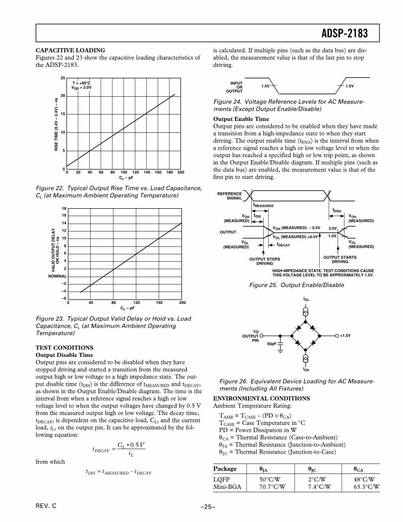
TEST CONDITIONSOutput Disable TimeOutput pins are considered to be disabled when they havestopped driving and started a transition from the measuredoutput high or low voltage to a high impedance state. The out-put disable time (tDIS) is the difference of tMEASURED and tDECAY,as shown in the Output Enable/Disable diagram. The time is theinterval from when a reference signal reaches a high or lowvoltage level to when the output voltages have changed by 0.5 Vfrom the measured output high or low voltage. The decay time,tDECAY, is dependent on the capacitive load, CL, and the currentload, iL, on the output pin. It can be approximated by the fol-lowing equation:
tDECAY = CL • 0.5V
iL
from which
tDIS = tMEASURED – tDECAY
is calculated. If multiple pins (such as the data bus) are dis-abled, the measurement value is that of the last pin to stopdriving.
1.5VINPUT
OROUTPUT
1.5V
Figure 24. Voltage Reference Levels for AC Measure-ments (Except Output Enable/Disable)
Output Enable TimeOutput pins are considered to be enabled when they have madea transition from a high-impedance state to when they startdriving. The output enable time (tENA) is the interval from whena reference signal reaches a high or low voltage level to when theoutput has reached a specified high or low trip point, as shownin the Output Enable/Disable diagram. If multiple pins (such asthe data bus) are enabled, the measurement value is that of thefirst pin to start driving.
2.0V
1.0V
tENA
REFERENCESIGNAL
OUTPUT
tDECAY
VOH(MEASURED)
OUTPUT STOPSDRIVING
OUTPUT STARTSDRIVING
tDIS
tMEASURED
VOL(MEASURED)
VOH (MEASURED) – 0.5V
VOL (MEASURED) +0.5V
HIGH-IMPEDANCE STATE. TEST CONDITIONS CAUSETHIS VOLTAGE LEVEL TO BE APPROXIMATELY 1.5V.
VOH(MEASURED)
VOL(MEASURED)
Figure 25. Output Enable/Disable
TOOUTPUT
PIN50pF
+1.5V
IOH
IOL
Figure 26. Equivalent Device Loading for AC Measure-ments (Including All Fixtures)
ENVIRONMENTAL CONDITIONSAmbient Temperature Rating:
TAMB = TCASE – (PD × θCA)TCASE = Case Temperature in °CPD = Power Dissipation in WθCA = Thermal Resistance (Case-to-Ambient)θ JA = Thermal Resistance (Junction-to-Ambient)θ JC = Thermal Resistance (Junction-to-Case)
Package JA JC CA
LQFP 50°C/W 2°C/W 48°C/WMini-BGA 70.7°C/W 7.4°C/W 63.3°C/W

ADSP-2183
–26– REV. C
128-Lead LQFP Package Pinout
92
93
95
90
91
88
89
87
96
86
94
81
82
83
84
79
80
78
76
77
85
75
73
74
71
72
69
70
67
68
66
65
98
99
101
97
102
100
41 42 43 44 46 47 48 4939 4540 626160 6463595550 51 52 53 54 56 57 58
11
10
16
15
14
13
18
17
20
19
22
21
12
24
23
26
25
28
27
30
29
32
31
5
4
3
2
7
6
9
8
1
34
33
36
35
38
37
120
121
122
123
124
125
126
127
128
119
111
118
117
116
115
114
113
112
110
109
108
107
106
105
104
103
PIN 1IDENTIFIER
TOP VIEW(Not to Scale)
IS GN
D
PF
4
PF
5
PF
6
PF
7
IAD
0
IAD
1
IAD
2
IAD
3
IAD
4
IAD
5
GN
D
VD
D
IAD
6
IAD
7
IAD
8
IAD
9
IAD
10
IAD
11
PW
DA
CK
IAC
K
BG
HV
DD
GN
D
IRQ
L0
IRQ
L1
FL
0
FL
1
FL
2
DT
0
TF
S0
RF
S0
DR
0
SC
LK
0
DT
1/F
0
TF
S1
/IR
Q1
RF
S1/
IRQ
0
GN
D
GND
D23
D22
D21
D20
D19
D18
D17
D16
D15
GND
VDD
GND
D5
GND
D4
D3
D2
D1
D0
VDD
IAL
PF3
PF2
PF1
PF0
WR
RD
IOMS
BMS
DMS
CMS
GND
VDD
PMS
A0
A1
A2
A3
A4
A5
A6
A7
XTAL
CLKIN
GND
CLKOUT
GND
VDD
A8
A9
A10
A11
DR
1/F
I
SC
LK
1
ER
ES
ET
RE
SE
T
EM
SE
E
BM
OD
E
BG
EBG
IAD
12
IAD
13
IAD
14
IAD
15
IRD
IWR
D14
D13
D12
D11
D10
D9
D8
D7
D6
ADSP-2183
A12
A13
IRQE
MMAP
PWD
IRQ2
BR
EBR
EINT
ELIN
ELOUT
ECLK

ADSP-2183
–27–REV. C
LQFP Pin Configurations
LQFP Pin LQFP Pin LQFP Pin LQFP PinNumber Name Number Name Number Name Number Name
1 IAL 33 A12 65 ECLK 97 D192 PF3 34 A13 66 ELOUT 98 D203 PF2 35 IRQE 67 ELIN 99 D214 PF1 36 MMAP 68 EINT 100 D225 PF0 37 PWD 69 EBR 101 D236 WR 38 IRQ2 70 BR 102 GND7 RD 39 BMODE 71 EBG 103 IWR8 IOMS 40 PWDACK 72 BG 104 IRD9 BMS 41 IACK 73 VDD 105 IAD1510 DMS 42 BGH 74 D0 106 IAD1411 CMS 43 VDD 75 D1 107 IAD1312 GND 44 GND 76 D2 108 IAD1213 VDD 45 IRQL0 77 D3 109 IAD1114 PMS 46 IRQL1 78 D4 110 IAD1015 A0 47 FL0 79 GND 111 IAD916 A1 48 FL1 80 D5 112 IAD817 A2 49 FL2 81 D6 113 IAD718 A3 50 DT0 82 D7 114 IAD619 A4 51 TFS0 83 D8 115 VDD20 A5 52 RFS0 84 D9 116 GND21 A6 53 DR0 85 D10 117 IAD522 A7 54 SCLK0 86 D11 118 IAD423 XTAL 55 DT1/F0 87 D12 119 IAD324 CLKIN 56 TFS1/IRQ1 88 D13 120 IAD225 GND 57 RFS1/IRQ0 89 D14 121 IAD126 CLKOUT 58 GND 90 GND 122 IAD027 GND 59 DR1/FI 91 VDD 123 PF728 VDD 60 SCLK1 92 GND 124 PF629 A8 61 ERESET 93 D15 125 PF530 A9 62 RESET 94 D16 126 PF431 A10 63 EMS 95 D17 127 GND32 A11 64 EE 96 D18 128 IS

ADSP-2183
–28– REV. C
144-Lead Mini-BGA Package Pinout(Bottom View)
12 11 10 9 8 7 6 5 4 3 2 1
A
B
C
D
E
F
G
H
J
K
L
M
GND GND IWR IS
IRDD21 D23 IAD15 IAD11 VDD GND IAD1 PF5 GND PF3 PF1
WR RDD17 D20 D22 IAD13 IAD8 VDD IAD0 PF4 PF2 PF0
IOMS DMSGND D15 D18 D19 D16 IAD9 IAD5 PF7 GND GND
CMS BMSD14 GND VDD GND GND IAD7 IAD3 A0 VDD VDD
PMSD10 D11 D13 D12 IAD12 D8 IAD4 A3 A4 A1 A2
IRQL0GND D2 GND D0 D3 DT1 VDD GND GND GND CLKIN
IRQL1VDD D1 BG RFS1 SCLK0 VDD VDD A10 VDD CLKOUTVDD
EBG BR EBR ERESET SCLK1 TFS1 TFS0 FL2 PWDACK A11 A12 A9
EINT RESET IACK IRQEELOUT ELIN GND DR0 FL0 GND MMAP A13
EMS BGH IRQ2 PWDECLK EE DR1 GND RFS0 FL1 GND BMODE
IAD14 IAD10 IAD6 GND IAD2 PF6 GND IAL
D6 D5 D9 D4 D7 DT0 A7 A8 A6 GND A5 XTAL

ADSP-2183
–29–REV. C
Mini-BGA Pin Configurations
Ball # Name Ball # Name Ball # Name Ball # Name
A01 IAL D01 GND G01 XTAL K01 A9A02 IS D02 DMS G02 A5 K02 A12A03 GND D03 GND G03 GND K03 A11A04 PF6 D04 IOMS G04 A6 K04 PWDACKA05 IAD2 D05 PF7 G05 A8 K05 FL2A06 GND D06 IAD5 G06 A7 K06 TFS0A07 IAD6 D07 IAD9 G07 DT0 K07 TFS1A08 IAD10 D08 D16 G08 D7 K08 SCLK1A09 IAD14 D09 D19 G09 D4 K09 ERESETA10 IWR D10 D18 G10 D9 K10 EBRA11 GND D11 D15 G11 D5 K11 BRA12 GND D12 GND G12 D6 K12 EBGB01 PF1 E01 VDD H01 CLKIN L01 A13B02 PF3 E02 VDD H02 GND L02 MMAPB03 GND E03 A0 H03 GND L03 IRQEB04 PF5 E04 BMS H04 GND L04 IACKB05 IAD1 E05 IAD3 H05 VDD L05 GNDB06 GND E06 CMS H06 IRQL0 L06 FL0B07 VDD E07 IAD7 H07 DT1 L07 DR0B08 IAD11 E08 GND H08 D3 L08 GNDB09 IAD15 E09 GND H09 D0 L09 RESETB10 IRD E10 VDD H10 GND L10 ELINB11 D23 E11 GND H11 D2 L11 ELOUTB12 D21 E12 D14 H12 GND L12 EINTC01 RD F01 A2 J01 CLKOUT M01 PWDC02 PF0 F02 A1 J02 VDD M02 IRQ2C03 WR F03 A4 J03 A10 M03 BMODEC04 PF2 F04 A3 J04 VDD M04 BGHC05 PF4 F05 PMS J05 VDD M05 GNDC06 IAD0 F06 IAD4 J06 IRQL1 M06 FL1C07 VDD F07 D8 J07 SCLK0 M07 RFS0C08 IAD8 F08 IAD12 J08 RFS1 M08 GNDC09 IAD13 F09 D12 J09 BG M09 DR1C10 D22 F10 D13 J10 D1 M10 EMSC11 D20 F11 D11 J11 VDD M11 EEC12 D17 F12 D10 J12 VDD M12 ECLK

ADSP-2183
–30– REV. C
OUTLINE DIMENSIONSDimensions given in mm and (inches).
128-Lead Metric Plastic Thin Quad Flatpack (LQFP)(ST-128)
TOP VIEW(PINS DOWN)
0.27 (0.011)0.22 (0.009)0.17 (0.007)
14.10 (0.555)14.00 (0.551)13.90 (0.547)
22.2
0 (0
.874
)22
.00
(0.8
66)
21.8
0 (0
.858
)
1
3839
6564
102128
0.50 (0.020)BSC
LEAD PITCH
103
20.1
0 (0
.792
)20
.00
(0.7
87)
19.9
0 (0
.783
)
16.20 (0.638)16.00 (0.630)15.80 (0.622)
SEATINGPLANE
1.60 (0.063)MAX
0.75 (0.030)
0.60 (0.024)0.50 (0.020)
1.45 (0.057)1.40 (0.055)1.35 (0.053)
0.15 (0.006)0.05 (0.002)
0.08 (0.003)MAX LEAD
COPLANARITY
LEAD WIDTH
NOTES:THE ACTUAL POSITION OF EACH LEAD IS WITHIN 0.08(0.0032) FROM ITS IDEAL POSITION WHEN MEASURED IN THELATERAL DIRECTION.CENTER FIGURES ARE TYPICAL UNLESS OTHERWISE NOTED

ADSP-2183
–31–REV. C
ORDERING GUIDE
Ambient InstructionTemperature Rate Package Package
Part Number Range (MHz) Description Option
ADSP-2183KST-115 0°C to +70°C 28.8 128-Lead LQFP ST-128ADSP-2183BST-115 –40°C to +85°C 28.8 128-Lead LQFP ST-128ADSP-2183KST-133 0°C to +70°C 33.3 128-Lead LQFP ST-128ADSP-2183BST-133 –40°C to +85°C 33.3 128-Lead LQFP ST-128ADSP-2183KST-160 0°C to +70°C 40 128-Lead LQFP ST-128ADSP-2183BST-160 –40°C to +85°C 40 128-Lead LQFP ST-128ADSP-2183KST-210 0°C to +70°C 52 128-Lead LQFP ST-128ADSP-2183KCA-210 0°C to +70°C 52 144-Lead Mini-BGA CA-144
OUTLINE DIMENSIONSDimensions given in mm and (inches).
144-Lead Mini-BGA Package Pinout(CA-144)
SEATINGPLANE
0.034 (0.85) MIN
0.010 (0.25) MIN
DETAIL A
0.022 (0.55)0.020 (0.50)0.018 (0.45)
BALL DIAMETER
0.005(0.12)MAX
0.010(0.25)NOM
0.067 (1.70) MAX
DETAIL A
0.031(0.80)BSC
0.346(8.80)BSC
0.031 (0.80) BSC 0.346 (8.80) BSC
ABCDEFGHJKLM
12 11 10 9 8 7 6 5 4 3 2 1
TOP VIEW
0.404 (10.25) 0.394 (10.00) SQ 0.384 (9.75)
0.404 (10.25)0.394 (10.00) SQ0.384 (9.75)
NOTETHE ACTUAL POSITION OF THE BALL POPULATIONIS WITHIN 0.006 (0.150) OF ITS IDEAL POSITIONRELATIVE TO THE PACKAGE EDGES. THE ACTUALPOSITION OF EACH BALL IS WITHIN 0.003 (0.08) OFITS IDEAL POSITION RELATIVE TO THE BALL POPULATION.
C00
184b
–0–7
/00
(rev
. C)
PR
INT
ED
IN U
.S.A
.