ds30 – ds5x - actionarielectrice.ro technologies... · the information in this document replace...
TRANSCRIPT

DS30 – DS5x ( Hardware rev. 1.20 Firmware rev. 1.09 )
Programmable stepper motor drives with integrated Modbus-RTU field bus
User’s Manual

The information in this document replace any other material previously published. LAM Technologies reserves the right to change technical specification and price to any product here at any time and without further notice. This manual contains reserved and proprietary information. All rights are reserved. It may not be copied, disclosed or used for any purposes not expressly authorized by LAM Technologies. LAM Technologies warrants the products herein against defects in materials and workmanship for a period of 12 months. This warranty does not apply to defects resulting from an improper use, inadequate installation or maintenance. This warranty also does not apply in case the products are received modified or integrated with other parts and/or products not expressly authorized or provided for by LAM Technologies. This warranty also does not apply in case the product’s label has been removed or modified. Any assistance request must be addressed to the product’s purchase source. In case of direct purchase from LAM Technologies a returned material authorization number (RMA) must be obtained from [email protected] clearly specifying the product code, the serial number, the problem found and the assistance required. The RMA will have to be clearly stated on each shipping documents otherwise the parcel could be rejected. The customer shall be responsible for the packaging and shipping of the defective product to LAM Technologies and the shipment must be made charges prepaid. The product inspected, repaired or substituted will be available to be collected at LAM Technologies’. During and within the warranty period, LAM Technologies can, on its judgment, repair or substitute the product. The cost of material and labor will not be charged within the warranty period. The above warranty also does not apply to the software. LAM Technologies shall not be liable for any direct or indirect damages such as, but not limited to, costs of removal and installation, lost profits, coming from the use or the impossibility to use the software. This manual is intended for skilled technical staff. In case the arguments, the terms and the concepts should not be clear you can contact [email protected]. It is forbidden to use the products herein described without being sure to have understood characteristics, installation and use procedures. Even though products described have been designed with extreme care, they are not intended or authorized for use as components in applications intended to support or sustain life and in application in which the failure of the product could create a situation where injury or death may occur to people or animals. LAM Technologies shall not be liable for any direct or indirect damages coming from the use of its products. The information in this manual have been carefully checked and are believed to be accurate, however any suggestion to improve it will be highly appreciated. LAM Technologies is a registered trade mark. Contacts:
• General information: [email protected] • Technical support: [email protected] • Sales information: [email protected]

DS30 – DS5x
1 NOTES, TERMS AND WARNINGS ..................................................................................................................... 7
2 RISKS AND PRECAUTIONS ............................................................................................................................... 9
3 INTRODUCTION ............................................................................................................................................ 11
3.1 PRODUCT DESCRIPTION ............................................................................................................................................. 11 3.1.1 Available models ....................................................................................................................................... 12 3.1.2 Main Features ........................................................................................................................................... 13
3.2 ACCESSORIES .......................................................................................................................................................... 14
4 INSTALLATION .............................................................................................................................................. 15
4.1 INSPECTION ............................................................................................................................................................ 15 4.2 MECHANICAL INSTALLATION ...................................................................................................................................... 15 4.3 AIR COOLING .......................................................................................................................................................... 18 4.4 WIRING ................................................................................................................................................................. 20
4.4.1 Power Supply: AC models .......................................................................................................................... 22 4.4.2 Power Supply: DC models .......................................................................................................................... 27 4.4.3 Motor ........................................................................................................................................................ 33 4.4.4 Control Signals .......................................................................................................................................... 35
4.4.4.1 Fiedlbus (DS5x series) .......................................................................................................................................35 4.4.4.1.1 DS50 series (RS485 - Modbus RTU) .............................................................................................................35 4.4.4.1.2 DS52 series (RS232 - Modbus RTU) .............................................................................................................37 4.4.4.1.3 DS54 series (USB - Modbus RTU) .................................................................................................................38
4.4.4.2 Digital inputs .....................................................................................................................................................39 4.4.4.3 Digital outputs ..................................................................................................................................................42 4.4.4.4 Analog inputs ....................................................................................................................................................44 4.4.4.5 Analog outputs .................................................................................................................................................45 4.4.4.6 Connection examples (PNP, NPN and Line Driver) ...........................................................................................46
4.4.4.6.1 Inputs ..........................................................................................................................................................46 4.4.4.6.2 Outputs........................................................................................................................................................47
4.4.5 Chassis setting........................................................................................................................................... 48
5 FUNCTIONALITY AND CONFIGURATION ......................................................................................................... 51
5.1 GENERAL DESCRIPTION ............................................................................................................................................. 51 5.2 PHASE CURRENT ...................................................................................................................................................... 52 5.3 AUTOMATIC CURRENT REDUCTION .............................................................................................................................. 54 5.4 CURRENT WAVEFORM MODIFICATION .......................................................................................................................... 56 5.5 ALARMS AND PROTECTIONS CONDITIONING .................................................................................................................. 56 5.6 SIGNAL LEDS .......................................................................................................................................................... 58 5.7 PROTECTIONS ......................................................................................................................................................... 60
5.7.1 General description ................................................................................................................................... 60 5.7.2 Under voltage ........................................................................................................................................... 60 5.7.3 Over voltage .............................................................................................................................................. 62 5.7.4 Over temperature ..................................................................................................................................... 64 5.7.5 Phase-to-phase short circuit ..................................................................................................................... 64 5.7.6 Phase-to-ground short circuit ................................................................................................................... 65 5.7.7 Phase-to-Vp short circuit (Vac) ................................................................................................................. 65 5.7.8 Interrupted phase A, interrupted phase B ................................................................................................. 65
6 PROGRAMMING ........................................................................................................................................... 67
6.1 OVERVIEW ............................................................................................................................................................. 67 6.2 CONTROL HARDWARE SIGNALS ................................................................................................................................... 68 6.3 SYSTEM REGISTERS ................................................................................................................................................... 70
6.3.1 Description of each single register ............................................................................................................ 71 6.3.1.1 RefVel ...............................................................................................................................................................71 6.3.1.2 Velocity .............................................................................................................................................................71 6.3.1.3 TargetPos ..........................................................................................................................................................71 6.3.1.4 Position .............................................................................................................................................................71 6.3.1.5 CPosition ...........................................................................................................................................................72 6.3.1.6 MaxVel ..............................................................................................................................................................72

DS30 – DS5x
6.3.1.7 Acceleration ......................................................................................................................................................72 6.3.1.8 Deceleration .....................................................................................................................................................73 6.3.1.9 ControlMode ....................................................................................................................................................73 6.3.1.10 PhaseCurrent ....................................................................................................................................................73 6.3.1.11 StByCurrent_Time .............................................................................................................................................74 6.3.1.12 StByCurrent_Percentage ..................................................................................................................................74 6.3.1.13 TimerA ..............................................................................................................................................................74 6.3.1.14 CounterA...........................................................................................................................................................74 6.3.1.15 Status ................................................................................................................................................................75 6.3.1.16 ControlFlags ......................................................................................................................................................76 6.3.1.17 Fault ..................................................................................................................................................................76 6.3.1.18 Error ..................................................................................................................................................................77 6.3.1.19 bEnable .............................................................................................................................................................77 6.3.1.20 bInPosition ........................................................................................................................................................77 6.3.1.21 bInStop .............................................................................................................................................................78 6.3.1.22 bEnabled ...........................................................................................................................................................78 6.3.1.23 bFault ................................................................................................................................................................78 6.3.1.24 bUVarLoaded ....................................................................................................................................................78 6.3.1.25 bUVarSaved ......................................................................................................................................................79 6.3.1.26 DigitalInput(0)..(3) ............................................................................................................................................79 6.3.1.27 DigitalInput(4)..(5) ............................................................................................................................................79 6.3.1.28 DigitalInputsA ...................................................................................................................................................80 6.3.1.29 DigitalOutput(0)..(1) .........................................................................................................................................80 6.3.1.30 DigitalOutputsA ................................................................................................................................................80 6.3.1.31 AnalogInput(0)..(1) ...........................................................................................................................................81 6.3.1.32 AnalogOutput(0) ...............................................................................................................................................81
6.4 VARIABLES ............................................................................................................................................................. 81 6.5 CONSTANTS ............................................................................................................................................................ 82 6.6 INSTRUCTION BLOCKS ............................................................................................................................................... 82
6.6.1 Assignment ............................................................................................................................................... 82 6.6.1.1 Unconditional ...................................................................................................................................................82 6.6.1.2 Conditioning .....................................................................................................................................................83
6.6.2 Function .................................................................................................................................................... 83 6.6.2.1 Save Variables in Flash ......................................................................................................................................83 6.6.2.2 Reset User Program ..........................................................................................................................................84
6.6.3 Jump .......................................................................................................................................................... 84 6.6.3.1 Unconditional jump ..........................................................................................................................................84 6.6.3.2 Conditional jump ..............................................................................................................................................85
6.6.4 Wait until .................................................................................................................................................. 86 6.6.5 Delay ......................................................................................................................................................... 87 6.6.6 Return ....................................................................................................................................................... 88 6.6.7 Mathematics ............................................................................................................................................. 89 6.6.8 Logic operations ........................................................................................................................................ 90
6.7 COMMON PROGRAMMING CONSTRUCT ....................................................................................................................... 91 6.7.1 Loop .......................................................................................................................................................... 91 6.7.2 Delay without suspend program execution .............................................................................................. 92 6.7.3 For .. Next cycle ......................................................................................................................................... 93 6.7.4 If …Then…Else ........................................................................................................................................... 94 6.7.5 Hysteresis .................................................................................................................................................. 95 6.7.6 Constraint of a value ................................................................................................................................. 96 6.7.7 CounterA extension on 32bits ................................................................................................................... 97
7 FIELDBUS ...................................................................................................................................................... 98
7.1 GENERAL DESCRIPTION ............................................................................................................................................. 98 7.2 MODBUS-RTU COMMUNICATION PROTOCOL ............................................................................................................... 98
7.2.1 Data structure (frame) ............................................................................................................................ 100 7.2.2 Data processing (frame) ......................................................................................................................... 100 7.2.3 Checksum computation (CRC) ................................................................................................................. 101 7.2.4 Data organization ................................................................................................................................... 102
7.2.4.1 bit....................................................................................................................................................................102 7.2.4.2 byte .................................................................................................................................................................102 7.2.4.3 word ...............................................................................................................................................................103

DS30 – DS5x
7.2.4.4 3byte ...............................................................................................................................................................103 7.2.4.5 dword .............................................................................................................................................................105
7.2.5 Supported functions ................................................................................................................................ 106 7.2.5.1 0x03, Reading of registers and variables (Read Holding Registers) ................................................................106 7.2.5.2 0x10, Writing of registers and variables (Write Multiple Registers) ...............................................................108 7.2.5.3 0x16, Changing of the bits of a register (Mask Write Registers) .....................................................................109
7.3 MAP OF THE REGISTERS AND USER’S VARIABLE ............................................................................................................ 111 7.3.1 RegTableVer ............................................................................................................................................ 112 7.3.2 ProductCode ............................................................................................................................................ 112 7.3.3 FirmwareVer ........................................................................................................................................... 112 7.3.4 HardwareRev .......................................................................................................................................... 113 7.3.5 SpecialVersion ......................................................................................................................................... 113 7.3.6 SerialNumber .......................................................................................................................................... 113
8 TECHNICAL DATA ........................................................................................................................................ 115


DS30 – DS5x Notes, Terms and Warnings
7
1 Notes, Terms and Warnings In this manual some symbols, whose meaning is listed below, are used to underline particular arguments. There is a dangerous condition which must be accurately evaluated and avoided. The not-respect of indications marked with this symbol can cause serious damages and injury to people, animals and things. The subject is very wide and could require a deeper examination with the technical support. The non-observation of what described could damage the products. Features and functionalities which cannot be easily found in other products. A shortcut to reach a target is shown. A change or repairing intervention which can be made directly by the user. An aspect connected to the temperature or longevity of the product.
!

Notes, Terms and Warnings DS30 – DS5x
8
The terms listed below are also used:
Product The microstepping drive described herein.
User Who selects and/or installs and/or uses the product.
Application The machine, the equipment, the device, etc. on which the product is applied.

DS30 – DS5x Risks and Precautions
9
2 Risks and Precautions
A T T E N T I O N Following are listed the most important warnings to be fully comprehended and applied by the user who, in case of non-complete comprehension or impossibility to apply them correctly, must not use the product at all.
The DS30 – DS5x drives are components. It is the user’s responsibility as the installer to be sure the product complies with the rules and regulations in force. The user must also be trained in the installation of the electronic equipment to fully comprehend the features, the calibration parameters and the indications contents of this guide. The user must provide for the application of all the local safety laws and regulations in force in the Country and/or application in which the product is used.
The user must provide that the product is inaccessible while powered on. The user must also consider that, because of the capacitors inside the drive, it is necessary to wait at least for 30 seconds after the power off before acceding to the drive. According to the external capacitors eventually mounted on the power supply circuit, it is possible the user shall have to wait for a longer time.
While working the product generates heat which can raise the temperature of some parts (as the heat sink, for example) up to values that can cause burns. Such a conditions remains for a long time even after the product has been powered off. The user must provide for the appropriate protections and signals, must train the operator, the technical support and risk maintenance staff, and then must indicate it in the service manual of the finished product.
The high performance drive is able to generate rapid accelerations with high motor torque. Never touch any mechanical part while the drive is powered on. The user must prearrange the application in order this condition is always granted.
!
!
!
!

Risks and Precautions DS30 – DS5x
10
The power supply of the product must be isolated from the electrical net. The user must always place a protective fuse in series to the power supply circuit.
The control signals are isolated from the power supply during normal working; anyway, during the designing of the application, the eventuality that in case of breakdown these lines could reach the same potential as the power supply, must be considered to meet safety requirements.
The product could be permanently damaged by corrosive substances (such as gas, salts, etc.), liquids or conductive dusts. Even a long and constant exposure to strong vibrations could cause the damage.
During some damage conditions the drive could emit sparks and fire. The cabinet and the nearby components must be chosen to tolerate this eventuality and to avoid propagation of flames to the application.
The products cannot be used in life support applications or where the failure of the products could cause death or injury to people, animals or things, or economic losses. The user not able to assure this condition must not use the products herein described.
Do not dismantle the product, do not try and repair it and do not modify it without being expressly authorized by LAM Technologies.
If the product is used in any manner that does not comply with the instructions given in this manual, then the product could be permanently damaged. For example, the product could be permanently damaged if power supplied with voltage superior to the allowed one, if supply polarity is inverted, if the motor is connected or disconnected while the drive is operating, and so on.
!
!
!
!
!
!
!

DS30 – DS5x Introduction
11
3 Introduction
3.1 Product description The DS30 – DS5x series drives integrate a built-in flexible programmable motion controller able to perform accurate motor control both in speed and in position. The programming is quick and simple and it is made putting in sequence the various functional blocks available in the UDP Commander development software tool, such as assignment blocks, conditional jump blocks, etc. Particularly powerful are the mathematical blocks able to execute additions, subtractions, multiplications and divisions and which allow to realize even complex applications. The connection with the external devices is through 4 inputs and 2 digital outputs each one optocoupled, independently PNP or NPN or line driver usable. Two +/-10V analog inputs and one 0-10Vdc analog output complete the available interface signals. Suitable for the bi-polar mode driving of two phase stepper motors at 4, 6 or 8 wires), the DS30 – DS5x series drives feature an accurate current control which assures a correct and smoothness movement of the motor. The use of last generation power components, together with the development of an innovative current control technology, has made possible to reach high level of efficiency, to be compact sized and to reduce drive heating. The high technology present in the product has also allowed to overcome the previous full step or fractioned limited step solutions, offering at the same price a product able to drive in microstepping mode with an high step frequency. The DS30 – DS5x drives series is equipped with a special port called DUP, designed for the programming, the debug and diagnostics of the drive. Through this special device it is possible to download into the drive the application program, to visualize the content of registers, I/O signals, etc. The bundled drive software simply and quickly guides the user in all the programming phases and assists him during the diagnostics and application debug. Before starting to operate on the product be sure to have the latest software version. The use of last generation components and technologies, together with the computerized test made on each single unit, gives to the product high reliability and economic competitiveness.

Introduction DS30 – DS5x
12
3.1.1 Available models The DS30 – DS5x family drives are available in a complete range of models diversified according to the power supply voltage and the phase current delivered to the motor. Some of them are also available in the AC supply version, identified by the letter A at the end of the code (for example DSxx44A). All the models share the same functional features:
Model
AC power supply voltage
(Vac)
DC power supply voltage (Vdc)
Effective phase current
(Arms)
Peak phase current (Apk)
Min Max Min Max Min Max Min Max DS3041 --- --- 18 50 0.3 1.4 0.42 2.0 DS3041A 16 36 --- --- 0.3 1.4 0.42 2.0 DS3044 --- --- 20 50 1 4 1.4 5.6 DS3044A 18 36 --- --- 1 4 1.4 5.6 DS3048 --- --- 20 50 3 8 4.2 11.3 DS3048A 18 36 --- --- 3 8 4.2 11.3 DS3073 --- --- 24 90 0.8 3 1.1 4.2 DS3073A 20 65 --- --- 0.8 3 1.1 4.2 DS3076 --- --- 24 90 2 6 2.8 8.5 DS3076A 20 65 --- --- 2 6 2.8 8.5 DS3078 --- --- 24 90 4 10 5.6 14.1 DS3078A 20 65 --- --- 4 10 5.6 14.1 DS3084 --- --- 45 160 2 4 2.8 5.6 DS3084A 35 115 --- --- 2 4 2.8 5.6 DS3087 --- --- 45 160 4 8.5 5.6 12.0 DS3087A 35 115 --- --- 4 8.5 5.6 12.0 DS3098 --- --- 45 240 4 10 5.6 14.1 DS5x41 --- --- 18 50 0.3 1.4 0.42 2.0 DS5x41A 16 36 --- --- 0.3 1.4 0.42 2.0 DS5x44 --- --- 20 50 1 4 1.4 5.6 DS5x44A 18 36 --- --- 1 4 1.4 5.6 DS5x48 --- --- 20 50 3 8 4,2 11,3 DS5x48A 18 36 --- --- 3 8 4,2 11,3 DS5x73 --- --- 24 90 0,8 3 1,1 4,2 DS5x73A 20 65 --- --- 0,8 3 1,1 4,2 DS5x76 --- --- 24 90 2 6 2,8 8,5 DS5x76A 20 65 --- --- 2 6 2,8 8,5 DS5x78 --- --- 24 90 4 10 5,6 14,1 DS5x78A 20 65 --- --- 4 10 5,6 14,1 DS5x84 --- --- 45 160 2 4 2,8 5,6 DS5x84A 35 115 --- --- 2 4 2,8 5,6 DS5x87 --- --- 45 160 4 8,5 5,6 12,0 DS5x87A 35 115 --- --- 4 8,5 5,6 12,0 DS5x98 45 240 45 240 4 10 5.6 14.1

DS30 – DS5x Introduction
13
3.1.2 Main Features
Simple programming at blocks Mathematical functions at 32bit Speed or position control Independent acceleration and deceleration ramps Absolute or relative positioning Resolution up to 3000rpm at 1/128 step/rev Quote from -2,147,483,638 to +2,147,483,647 Four digital inputs and two +/-10V analog inputs Two digital outputs and one 0-10V analog output Optocoupled and differential I/O, independently NPN or PNP usable Analog inputs at 11bit Digital inputs from 3Vdc up to 28Vdc with current regulator Line driving supported Protective diode for inductive loads on each digital output Automatic current reduction settable from 0% up to 100% with increments of 10% Wide range of power supply Single power supply voltage for the whole drive Current setting with increments of 0.1Arms Accurate current control Resonance damping High efficiency, low losses and contained heating Colored and numbered removable terminal blocks for easy and fast wiring Complete diagnostics Over/under voltage protections Phase to phase short circuit protection both direct and crossed Phase to ground short circuit protection Positive supply short circuit protection Thermal protection Interrupted phase alarm independent for each phase Univocal indication for each anomaly Malfunctioning status LED indicator Motor qualification LED indicator Power supply LED indicator Digital development PC based simple setting PC based diagnostics Compact size Simple and fast DIN rail mounting Low cost

Introduction DS30 – DS5x
14
3.2 Accessories The UDP30 interface is an essential accessory for the setting and diagnostics of the product. Each drive is sold complete of the removable terminal blocks, anyway in case of loss or breach it is possible to re-order them making reference to one of the following codes.
Code Description
UDP30 Setting and diagnostic interface LSP1004 DIN rail kit consisting of hook and spring LSP4002 Terminal blocks kit consisting of:
1pc. numbered removable terminal block, red color, 2 poles 1pc. numbered removable terminal block, grey color, 5 poles 1pc. numbered removable terminal block, grey color, 10 poles
LSP4004 5pcs. numbered removable terminal block, red color, 2 poles LSP4006 5pcs. numbered removable terminal block, grey color, 5 poles LSP4007 5pcs. numbered removable terminal block, grey color, 6 poles LSP4008 5pcs. numbered removable terminal block, grey color, 10
poles
DS30 – DS5x Installation
15
4 Installation
4.1 Inspection Verify that the drive is not damaged, the package is intact and all accessories are included. Furthermore, control that the drive code corresponds to the ordered one, eventual special and customized version included. In case of problems please address to the product’s vendor.
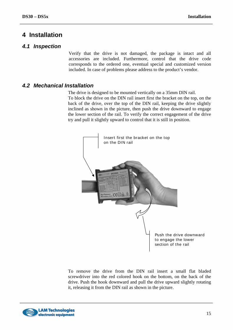
4.2 Mechanical Installation The drive is designed to be mounted vertically on a 35mm DIN rail. To block the drive on the DIN rail insert first the bracket on the top, on the back of the drive, over the top of the DIN rail, keeping the drive slightly inclined as shown in the picture, then push the drive downward to engage the lower section of the rail. To verify the correct engagement of the drive try and pull it slightly upward to control that it is still in position. To remove the drive from the DIN rail insert a small flat bladed screwdriver into the red colored hook on the bottom, on the back of the drive. Push the hook downward and pull the drive upward slightly rotating it, releasing it from the DIN rail as shown in the picture.
Insert first the bracket on the top on the DIN rail
Push the drive downward to engage the lower section of the rail

Installation DS30 – DS5x
16
The heat generated by the drive while operating must be dissipated toward the surrounding air. To help cooling, the drive must be installed vertically in an area with a sufficient air gap of about 50mm above and below the drive itself, with no obstructions (wiring cables are anyway allowed). No space needs to be left on the sides and more drives can be put side by side taking a very compact space. According to the drive calibration and to the running cycle, the space can be also substantially reduced without compromising the correct working of the drive.
Push the screwdriver slightly downward and pull the drive upward, releasing it from the DIN rail
Insert a small flat bladed screwdriver into the red colored hook

DS30 – DS5x Installation
17
DUP
ON EN ST FL
DS30xx
>50mm
>50mm
Drive
Space required for an easy heat cooling
Space required for an easy heat cooling

Installation DS30 – DS5x
18
4.3 Air cooling The product you have purchased has an exceptional efficiency that often allows the use even in the absence of forced ventilation. Whereas the drives is used with high calibration current or at high power supply voltage, whereas the working cycle is very heavy or the ambient temperature is high, it is possible to apply to forced ventilation to maintain the drive temperature whiting the functioning range values. The fan can be positioned over or under the drive. A lateral position is not recommended. Thanks to the compact size of the drive, one only and economic fan of 120mm x 120mm can supply air circulation sufficient for 6 drives simultaneously (models of 18mm wide).
DUP
ON EN ST FL
DS30xx
DUP
ON EN ST FL
DS30xx
DUP
ON EN ST FL
DS30xx
DUP
ON EN ST FL
DS30xx
DUP
ON EN ST FL
DS30xx
DUP
ON EN ST FL
DS30xx
105mm
Fan 120x120mm Air flow
direction

DS30 – DS5x Installation
19
In case of a reduced fan size, it must be set in a rear position and at about 30mm high from the drive. A nearer or more distant position could reduce its effectiveness. It is important to avoid the drive is covered with powder, dust or other. The buildup of such substances inside the drive could cause the malfunctioning or the breaking of the drive. Filters and necessary solutions must be got ready to avoid these damages to occur.
Not recommended position
Correct position
Air flow direction
30mm

Installation DS30 – DS5x
20
4.4 Wiring The use of numbered and colored movable terminal blocks makes easier the wiring of the drive. All the terminal blocks have 5mm pitch to allow an easy wiring of signal and power cables. All the terminal blocks do not contain iron and are supplied with mobile truck. The clamping screw is slotted head, sized for screwdriver of 3x0.6mm.
Terminal n. 1 Connector CN1
Terminal n. 1 Connector CN2
Terminal n. 1 Connector CN3
Terminal n. 1 Connector CN4

DS30 – DS5x Installation
21
We recommend to apply a tightening torque of about 0.8Nm. All terminals can tighten correctly cables with section between 0.1mm2 and 2.5mm2 (24…14 AWG). We recommend to skin off the cable for 7/8mm as shown in the figure below.
7/8mm
Apply a tightening torque of about 0.8Nm

Installation DS30 – DS5x
22
4.4.1 Power Supply: AC models
The AC supply drives are identified by the letter A placed at the end of the code (ex. DS3044A). They integrate a rectifier bridge and the filter condensers necessary to rectify and filter the AC power supply voltage. Therefore, this series of drives does not need an external power supply and can be directly connected to the output of a transformer with adequate voltage. These products can also be supplied in DC, however take present that the rectifier bridge inside does not allow to recover the energy produced by the motor during the deceleration. When supplying in DC a drive provided for the AC input, make reference to the parameters of the corresponding DC version (for example for the DS3076A refer to the DS3076) considering that the rectifier bridge inside has a total drop of about 3Vdc. This means that, if for example a drive provided for AC input is supplied with 35Vdc voltage, this will act, for the purpose of the applied voltage, as the corresponding supplied at about 32Vdc. The following table resumes the working and breaking effective voltage values considering a sinusoidal waveform.
Symbol Description Value Unit
Min Typ Max
Vac
Nominal AC supply voltage
DSxx41A 16 28 36
Vac
DSxx44A DSxx48A 18 32 36 DSxx73A DSxx76A DSxx78A
20 55 65
DSxx84A DSxx87A 35 110 115
Vacbrk
AC supply voltage causing the permanent damage
DSxx41A DSxx44A DSxx48A
42
DSxx73A DSxx76A DSxx78A
75
DSxx84A DSxx87A 142
Vach
Over voltage protection intervention threshold
DSxx41A DSxx41A 36.5 39 DSxx44A DSxx48A 40 42 DSxx73A DSxx76A DSxx78A
69 73
DSxx84A DSxx87A 120 126
Vacl
Under voltage protection intervention threshold
DSxx41A DSxx41A 12.5 14.5 DSxx44A DSxx48A 14 15.6 DSxx73A DSxx76A DSxx78A
16 18.6
DSxx84A DSxx87A 31 33.6 The power supply is connected by the grey colored two poles connector.

DS30 – DS5x Installation
23
The overcoming of the Vacbrk voltage limit damages permanently the drive. Do not install the drive before the wiring is complete.
For the connection with the transformer it is necessary to use a conductor with section adequate to the drive’s calibration (for safety’s it is better to use the max current supplied by the drive). The following table resumes the cable sections suggested for each drive:
Model Cable section (mm2)
DSxx41A 1 DSxx44A DSxx48A 2.5 DSxx73A 1 DSxx76A 1.5 DSxx78A 2.5 DSxx84A 1.5 DSxx87A 2.5
The power supply cable can be installed together with the ones connecting the drive to the motor. It is recommended not to place the power supply cable nearby the signal ones. While choosing the transformer secondary voltage it is important to take into account the maximum net fluctuation expected in the worst operative conditions, the maximum vacuum voltage and the minimum full load voltage and to ensure that the maximum and minimum values, result of the combination of these components, are within the maximum and minimum voltage values specified for the chosen drive model.
CN1 – Signal set-up (AC models) Contact n. Description
1 Vac, AC power supply voltage input 2 Vac, AC power supply voltage input
Terminal n. 2
Terminal n. 1
Vac
CN1

Installation DS30 – DS5x
24
The power that the transformer must handle is given by the one absorbed by the load (depending from the torque required to the motor as well as from the rotation speed), and by the motor and drive efficiency. The power lost on the drive for each model is indicated in the following table.
Model Min Typ Max Unit DSxx41A 7 W DSxx44A 12 W DSxx48A 21 W DSxx73A 10 W DSxx76A 20 W DSxx78A 24 W DSxx84A 20 W DSxx87A 36 W
The following is an example of base connection. The above scheme includes a three-phase transformer (note the distribution of the drives on the three phases). If necessary it is also possible to use a mono-phase transformer. Also note that the wiring must be star-like, where the earth connections of the various components ends in one only point electrically connected to the metal chassis and the earth of the plant.
PE
Protection and Command
L1 L2 L3 PE
+ Dr. 1- + Dr. 2 - . . . . + Dr. n -
Three-phase transformer with shield between primary and secondary
Filter
T1
Main Supply
Fuses
Fn

DS30 – DS5x Installation
25
Do not connect the transformer secondary to earth otherwise there is a risk of permanent damage to the drive due to the short circuit created between the transformer secondary and the ground of the drive (terminal 5 of connector CN2). As shown in the scheme, it is necessary to put in series to the transformer primary winding a filter able to stop the emissions coming from the drive and/or present on the main supply. Furthermore, the filter must be able to support the maximum power required by the drive plus the transformers losses. The reduction level the filter must guarantee can vary a lot according to the laws applied to the field to which the application and/or installation belongs. The producers of filters SHAFFNER and CORCOM can represent a good reference to find the right filter. It is obligatory to provide on each phase of the transformer primary winding a fuse able to intervene in case of short circuit or malfuctioning. It is also obligatory to use a fuse on each drives’ power supply conductor. The following table relates the suggested value for some components according to the number of drives present in the application. The calculation considers also an oscillation of the main supply voltage included within +10/-20%.

Installation DS30 – DS5x
26
Model
Fuses Fn
(A rit.)
Number of drives
Secondary T1 (Vac)
Power
T1 (VA)
DSxx41A
2
1
32
50
2 100 3 150
4..5 250 6..8 350
DSxx44A
6.3
1
32
125
2 250 3 375
4..5 600 6..8 900
DSxx48A
12.5
1
32
250
2 500 3 750
4..5 1100 6..8 1800
DSxx73A
4
1
55
150
2 300 3 450
4..5 700 6..8 1000
DSxx76A
8
1
55
300
2 600 3 900
4..5 1400 6..8 2100
DSxx78A
16
1
55
400
2 800 3 1200
4..5 1800 6..8 2800
DSxx84A
6.3
1
110
350
2 700 3 1050
4..5 1600 6..8 2500
DSxx87A
12.5
1
110
700
2 1400 3 2000
4..5 2500 6..8 5000
The working voltage of the T1 transformer primary winding must be chosen according to the main supply voltage available during the installation of the application. The transformer must have a shield between primary and secondary windings which must be connected to earth with a short and not inductive connection. The secondary winding voltage is

DS30 – DS5x Installation
27
meant without the load, with the primary winding supplied at the nominal voltage. In the configurations with more than a drive, if the drives are not all calibrated to the maximum current and/or if the working cycle is not simultaneous, the power of the transformer can be considerably reduced. In some cases this can also be made when the motors’ speed is limited. The set composed by the filter and the transformer must be used only to supply voltage to the drives. It is advised against deriving other supplies from any of these parts. On the contrary, it is suggested to get auxiliary supplies using directly the main supply upstream of the filter.
4.4.2 Power Supply: DC models The DC supply drives need a Vp voltage as specified in the table below. In the highest absorption conditions the power supply must grant a ripple voltage inferior to Vprp.
Symbol Description Value Unit Min Typ Max
Vp
Nominal DC supply voltage
DSxx41 18 45 50
Vdc DSxx44 DSxx48 20 45 50 DSxx73 DSxx76 DSxx78 24 80 90 DSxx84 DSxx87 45 140 160 DSxx98 45 200 240
Vprp
Allowed ripple voltage
DSxx41 DSxx44 DSxx48
8
Vpp DSxx73 DSxx76 DSxx78 15 DSxx84 DSxx87 25 DSxx98 30
Vpbrk
Voltage causing permanent damage
DSxx41 DSxx44 DSxx48
-0.5 58
Vdc DSxx73 DSxx76 DSxx78 -0.5 105 DSxx84 DSxx87 -0.5 200 DSxx98 -0.5 260
Vph
Over voltage protection intervention threshold
DSxx41 50.2 51.5
Vdc DSxx44 DSxx48 54 56 DSxx73 DSxx76 DSxx78 96 102 DSxx84 DSxx87 170 180 DSxx98 242 255
Vpl
Under voltage protection intervention threshold
DSxx41 16 17.8
Vdc DSxx44 DSxx48 18 19.5 DSxx73 DSxx76 DSxx78 21 23.5 DSxx84 DSxx87DSxx98 41 44

Installation DS30 – DS5x
28
The power supply is connected by the red colored 2 poles connector. The positive terminal must be connected to the terminal 1, while the negative terminal to the terminal 2. Reverse polarity connection damages permanently the drive, just as the overcoming of the Vpbrk voltage limit. Do not install the drive before the wiring is complete. Never connect the drive with the power supply turned on.
If the distance between the drive and the power supply is more than 3m, it is necessary to place near the drive (less than 10cm) an electrolytic capacitor whose characteristics are listed below:
Model C2 Voltage (Vdc)
C2 Capacity
(μF) DSxx41 63 470 DSxx44 63 470 DSxx48 63 1000 DSxx73 100 220 DSxx76 100 470 DSxx78 100 1000 DSxx84 200 470 DSxx87 200 1000 DSxx98 250 1000
To connect together the power supply, the drive and the eventual local capacitor, it is necessary to use a conductor with section adequate to the drive’s current calibration (anyway, for safety’s reason, it is better to use the maximum current supplied by the drive). The following table resumes the cable section suggested for each drive:
CN1 - Signals set-up (DC models) Contact n. Description
1 +Vp, positive DC supply voltage 2 -Vp (GND), negative DC supply voltage
Terminal n. 2
Terminal n. 1
+ -
CN1

DS30 – DS5x Installation
29
Model Cable section
(mm2) DSxx41 1 DSxx44 DSxx48 2.5 DSxx73 1 DSxx76 1.5 DSxx78 2.5 DSxx84 1.5 DSxx87 2.5 DSxx98 2.5
The power supply cable can be installed together with the ones connecting the drive to the motor. We recommend not to place the power supply cable nearby the signal ones. There are two types of power supplies commonly used, regulated and unregulated. The regulated power supply maintains a stable output voltage, immune to the net and load fluctuations, which allows to supply the drive even with voltage values near to the allowed maximum ones, with an immediate benefit in terms of torque supplied by the motor at high speed. The disadvantage of the regulated power supplies is their cost. An unregulated power supply is cheaper, but it requires the consideration of safety’s tolerance during its sizing so that, in presence of net and load fluctuations, voltage remains however within the acceptable working values. A detailed description about the sizing of the power supply is outside of this manual. The user who decides to construct its own power supply must be technically qualified to size it, to assure its correct working and to fulfill each safety requirements. To determine the power supply output voltage it must be considered the maximum net fluctuation expected on worse operating conditions, the maximum vacuum voltage and the minimum voltage at full load, and to assure that the values result of these components combination are within the range of the maximum and minimum voltage values specified for the chosen drive model. The power that the power supply must deliver is given by the one absorbed by the load (depending from the torque required to the motor as well as from the rotation speed), and by the motor and drive efficiency.

Installation DS30 – DS5x
30
The power lost on the drive for each model is indicated in the following table.
Model Min Typ Max Unit DSxx41 5 W DSxx44 8 W DSxx48 15 W DSxx73 8 W DSxx76 15 W DSxx78 15 W DSxx84 15 W DSxx87 20 W DSxx98 30 W
Because of the many variables in play it is clear the impossibility to prior indicate an only one kind of dimensioning valid for each application. Just for example, not to be considered exhaustive and correct for the application, see the following electric scheme of an unregulated power supply with a brief indication of the components value. Also note that the wiring must be star-like, where the earth connection of the various components ends in one only point electrically connected to the metal chassis and the earth of the plant. Also the wiring towards the drives must be star-like, with the center of the star on C1 capacitor poles. As shown in the scheme, it is necessary to put in series to the transformer primary winding a filter able to stop the emissions coming from the drive and/or present on the main supply. Furthermore, the filter must be able to support the maximum power required by the drive plus the transformers losses.
+ C1
Protection and Command
L1 L2 L3 PE
+ Dr. 1- + Dr. 2 - . . . . + Dr. n -
Three-phase transformer with shield between primary and secondary
Filter
T1
Rectifier Main Supply
D1
Fuses
Fn

DS30 – DS5x Installation
31
It is obligatory to provide on each phase of the transformer primary winding a fuse able to intervene in case of short circuit at the supply output or a malfunctioning of its parts. It is also obligatory to use a fuse on each drives’ power supply conductor. The reduction level the filter must guarantee can vary a lot according to the laws applied to the field to which the application and/or installation belongs. The producers of filters SHAFFNER and CORCOM can represent a good reference to find the right filter. The following table relates the characteristic values of the main components in the transformer. The calculation considers also an oscillation of the main supply voltage included within +10/-20%. You can also ask to your own vendor to evaluate if the following values are usable for your application.
Model
Fuses Fn
(A rit.)
Number of drives
Secondary T1 (Vac)
Power T1 (VA)
Current D1 (Arms)
Voltage C1 (Vdc)
Capacity C1 (μF)
DSxx41
2
1
32
50 25A
63
1000
2 100 25A 2200 3 150 25A 3300
4..5 250 25A 4700 6..8 350 25A 5600
DSxx44
6.3
1
32
125 25A
63
3300
2 250 25A 4700 3 375 25A 5600
4..5 600 25A 8200 6..8 900 35A 10000
DSxx48
12.5
1
32
250 25A
63
4700
2 500 25A 6800 3 750 25A 8200
4..5 1100 35A 10000 6..8 1800 50A 15000
DSxx73
4
1
55
150 25A
100
1800
2 300 25A 2200 3 450 25A 3300
4..5 700 25A 4700 6..8 1000 35A 5600
DSxx76
8
1
55
300 25A
100
2200
2 600 25A 3300 3 900 25A 3900
4..5 1400 35A 4700 6..8 2100 50A 6800

Installation DS30 – DS5x
32
DSxx78
16
1
55
400 25A
100
3300
2 800 25A 4700 3 1200 25A 5600
4..5 1800 35A 8200 6..8 2800 50A 10000
DSxx84
6.3
1
110
350 25A
200
1000
2 700 25A 1500 3 1050 25A 1800
4..5 1600 25A 2200 6..8 2500 35A 3300
DSxx87
12.5
1
110
700 25A
200
1500
2 1400 25A 2200 3 2000 25A 3300
4..5 2500 35A 4700 6..8 5000 50A 6800
DSxx98
16
1
140
1000 25A
250
1800
2 2000 25A 2200 3 3000 35A 3300
4..5 4500 50A 4700 6..8 7000 50A 6800
The values suggested for the capacitor C1 can also be obtained placing more capacitors in parallel amongst them. Eventual approximations must be made in excess. The user can add in parallel to the C1 capacitor a resistor, opportunely dimensioned, to discharge the capacitor more quickly. The working voltage of the T1 transformer primary winding must be chosen according to the main supply voltage available during the installation of the application. The transformer must have a shield between primary and secondary windings which must be connected to earth with a short and not inductive connection. The secondary winding voltage is meant without the load, with the primary winding supplied at the nominal voltage. The rectifier, besides supporting the maximum current required by the drive, must be able to tolerate the current supplied during the C1 capacitor charge. Such current, as being essentially limited only by the internal resistor of the transformer secondary winding, usually very low, and by the wiring, can also be of elevated entity, even if of short length (it exhausts when the capacitor is charged). Furthermore, the rectifier needs an heat sink able to maintain the temperature within the range defined by the manufacturer (usually 70°C). The working voltage of the D1 rectifier must be then chosen according to the T1 transformer secondary winding voltage multiplied at least by 2. In the configurations with more than a drive, if the drives are not all calibrated to the maximum current and/or if the working cycle is not simultaneous, the power of the transformer can be considerably reduced. In some cases this can also be made when the motors’ speed is limited.

DS30 – DS5x Installation
33
The diagram and the components values refer to a three-phase power supply. Dimensioning in a different way the components it is possible to realize a mono-phase power supply, which is not recommended when the required power is greater than 500W. The set composed by the filter, the transformer and the power supply must be used only to supply voltage to the drives. It is advised against deriving other supplies from any of these parts. On the contrary, it is suggested to get auxiliary supplies using directly the main supply upstream of the filter.
4.4.3 Motor The connection between the drive and the motor must be made using shielded cable and connecting the screen to the drive’s SHIELD terminal. The cable shield on the motor side must be connected to the motor body only if this one is electrically insulated from the structure where it is fastened. In case the motor is electrically earth connected (for example through a mechanical fastener) the motor side shield must not be connected. Only if problems connected to electromagnetic emissions occur it is possible to try and connect the shield also from the motor side. Because of the possible ground loops which could start, it is advised to execute this wiring only when strictly necessary. The drive regulates the current in the motor phases through the supply voltage modulation in chopper technique. The use of a good quality shielded cable and a correct wiring are essential to better reduce the electromagnetic emissions.
Shield wiring. It must be as much short as possible
Terminal n. 5
Terminal n. 1
CN2

Installation DS30 – DS5x
34
CN2 – Signals set-up Contact n. Description
1 FA-, negate output phase A 2 FA+, positive output phase A 3 FB+, positive output phase B 4 FB-, negate output phase B 5 SHIELD (internally connected with GND)
Inverting the FA+ phase with the FA- phase, or the FB+ phase with the FB- phase, the motor rotation direction is inverted (making both inversions the rotation does not change). The cable section can be dimensioned according to the drive current calibration, anyway it is suggested to choose a cable suitable for the maximum current deliverable from the chosen drive. It is also advised to connect the motor to the drive with a cable with a length inferior to 10m. For cables with a greater length, the cable size must be increased to counterbalance the voltage drop. The following table indicates the cable section suggested for each drive according to the cable length:
Model
Cable section (mm2) Cable length
<= 10m Cable length
> 10m DSxx41 0.5 1 DSxx44 1 1.5 DSxx48 1.5 2 DSxx73 1 1.5 DSxx76 1.5 2 DSxx78 2.5 3 DSxx84 1 1.5 DSxx87 1.5 2 DSxx98 2.5 3
The cable connecting the drive to the motor can be installed together with the power supply cable, but it must be kept separate from the signal ones. If difficulties are met to pass compatibility tests, it is possible to place in series to each phase an inductor with a value included between 10uH and 100uH and with current adequate to the set phase current. The inductor must be placed directly at the drive output.

DS30 – DS5x Installation
35
4.4.4 Control Signals The cable used for the control signals wiring must be a shielded-type.
4.4.4.1 Fiedlbus (DS5x series) The information contained in the following chapters apply only to the drives provided with fieldbus (DS50, DS52 and DS54 series). When the drive is supplied only through the UDP30, the RS485 or the RS232 fieldbus communication ports are not working.
4.4.4.1.1 DS50 series (RS485 - Modbus RTU) The DS50 series is equipped with a RS485 hardware interface, optoisolated from the power stage, and with a Modbus-RTU communication protocol. The connection to the bus is through a 9 pin female D-sub connector as required by the Modbus specifications. In the following representation is shown the signals arrangement on the 9 pin connector.
CN5 - Signals disposition Contact n. Description
1 signals common, it is the reference (0V) of the D0 and D1 signals
2 +5V, voltage referred to the 0V with max current of 10mA 3 not connected 4 not connected 5 D0, data line also called A/A’ or TxRx- 6 not connected 7 not connected 8 not connected 9 D1, data line also called B/B’ or TxRx+
For the connection it is suggested the use of a twisted pair cable.
1
6 9
5 CN5

Installation DS30 – DS5x
36
The connections 1 and 2 can be used to connect the RS485 polarization resistors if needed. Keep in mind that the max source current from the pin 2 is 10mA. The value suggested for the polarization resistors is between 1Kohm and 4K7ohm. If the length of the bus is high (usually more than 10m) it is sometimes necessary to insert the bus termination resistors. The suggested value for the termination resistors is between 120ohm and 330ohm. These resistors must be connected bewteen D0 and D1, to the extremes of the net. In the following picure both termination and polarization resistors can be seen.
Termination resistors 120ohm
Polarization resistors 1Kohm
D0 D1
pin5pin9pin1pin2
CN5
pin9pin5 CN5
pin5 CN5 pin9
PLC, PC, etc.

DS30 – DS5x Installation
37
4.4.4.1.2 DS52 series (RS232 - Modbus RTU) The DS52 series is equipped with a RS232 hardware interface, optoisolated from the power stage, and with a Modbus-RTU communication protocol. The connection to the bus is through a 9 pin female D-sub connector as required by the Modbus specifications. In the following representation is shown the signals disposition on the 9 pin connector.
CN5 - Signals disposition Contact n. Description
1 not connected 2 TXD, data transmitted by the drive 3 RXD, data received by the drive 4 not connected 5 signals common, it is the reference (0V) of the TXD and RXD
signals 6 not connected 7 not connected 8 not connected 9 not connected
For the connection to the master it is suggested the use of a shielded cable with a length not superior to 20m.
1
6 9
5 CN5

Installation DS30 – DS5x
38
4.4.4.1.3 DS54 series (USB - Modbus RTU) The DS54 series is equipped with an USB Full-Speed-type hardware interface, optoisolated from the power stage, and with a Modbus-RTU communication protocol. The USB interface is particularly suitable to control the drive through a PC. The bundled drive software allows to emulate a standard system serial port. This solution helps to write the communication program with the drive, which will be able to make use of all the provided standard functions to communicate through a system serial port. The drives currently supplied are for operating systems such as Windows 98, 98SE, Me, 2K, XP, Vista and Windows 7 (32 or 64 bit). The connection is through a standard female USB-B connector. In the following illustration is shown the signals disposition on the USB-B connector.
CN5 - Signals disposition Contact n. Description
1 Vbus, positive power supply coming from the PC 2 D-, negate data line 3 D+, data line 4 Ground, 0V reference for the signals and for Vbus
For the connection to the PC it is suggested to use a good quality shielded cable with a length not superior to 5m.
1
4 3
2 CN5

DS30 – DS5x Installation
39
4.4.4.2 Digital inputs The drive is provided with a total of 4 digital inputs referring to the CN3 10-poles connector (two poles are reserved to a digital output). The cable used for the wiring must be shielded-type. The shielding of the connecting cable must be connected only to the side of the numerical control device (PC, PLC or other), while on the side of the drive it must remain unconnected, as shown in the figure below.
CN3 - Signals Contact n. Description
1 DI0+ DigitalInput(0), positive 0 digital input 2 DI0- DigitalInput(0), negative 0 digital input 3 DI1+ DigitalInput(1), positive 1 digital input 4 DI1- DigitalInput(1), negative 1 digital input 5 DI2+ DigitalInput(2), positive 2 digital input 6 DI2- DigitalInput(2), negative 2 digital input 7 DI3+ DigitalInput(3), positive 3 digital input 8 DI3- DigitalInput(3), negative 3 digital input 9 DO0+ DigitalOutput(0), positive 0 digital output 10 DO0- DigitalOutput(0), negative 0 digital output
The section of the cable does not have much importance as the circulating currents are meager (in the order of few mA), therefore choose the section according to the wiring functionality. The control signal cable must not be placed together with the power supply or the motor cables. If it happens there is the possibility that the high slew rate voltage and the high rate current could be coupled with the logic level signal and corrupt it.
Terminal n. 1
Terminal n. 10
Shield to be left unconnected
CN3

Installation DS30 – DS5x
40
The digital inputs of the DS30 – DS5x drives can be independently connected in NPN or PNP logic or in line driving mode. Each input lays both the connections making possible mixed settings. All inputs are optocoupled amongst them, towards the motor and towards the power supply. The DS30 – DS5x drives have on each input a particular current limitation circuit which grants a constant absorption to the varying of the applied voltage. This device allows a wide input power supply range (from 3Vdc up to 28Vdc) without requiring excessive current to the control equipment or external limit resistor. A good number of drives nowadays on the market, of the same category, uses to place in series to the input a simple current limitation resistor which reduces the input working voltage setting and causes, moreover, high current values when the input voltage is high. The DS30 – DS5x drives, on the contrary, maintain an almost constant absorption on the whole working range, as shown in the diagram below.
+ -
Input signal
Drive
Current regulator. 6mA for the whole power supply range
1K5ohm for DI0 and DI1 1Kohm for DI2 and DI3
mA 24 18 12 6
3 12 24 28 Vdc
DS30 – DS5x drives: the current remains constant to the varying of the input voltage
Input with a simple 330ohm limitation resistor. The current rises over 80mA with 28Vdc

DS30 – DS5x Installation
41
Each single input can be used on line driving mode independently from the others. The following table resumes the electric characteristics of the control signals.
The overcoming of the Vdibrk voltage limit damages permanently the drive. Sometimes the Vdibrk voltage limit can be accidentally overcome because of the currents driven by the inductive loads present in the application and out of the recycle diode in anti-parallel. If the installation includes electro valves, contactor (remote control switch), electromagnetic brakes, etc. it is advised to place on each one of them a recycle diode, or to adopt a similar solution, to avoid the extra voltage produced when the inductive load switched off. If the same power supply is used to provide the power and the signal supply, for example a 24Vdc device, carefully verify that the energy produced by the motor during the braking does not increase the voltage at the ends of the power supply over the Vdibrk limit supported by the input.
Symbol Description Value Unit Min Typ Max
Vdi Active input voltage 3 28 Vdc Vdioff Inactive input voltage -30 1 Vdc Vdibrk Digital inputs breakdown voltage -30 +30 Vdc
Idi Current absorbed by the digital inputs (24Vdc) 4 6 8 mA

Installation DS30 – DS5x
42
4.4.4.3 Digital outputs The drive is provided with a total of two digital outputs. The DO0 output is available on the CN3 connector while the DO1 one on the CN4 connector, as shown in the representation below. The cable used for the wiring must be shielded-type. The shielding of the connecting cable must be connected only to the side of the numerical control device (PC, PLC or other), while on the side of the drive it must remain unconnected, as shown in the figure below.
CN3 - Signals Contact n. Description
1 DI0+ DigitalInput(0), positive 0 digital input 2 DI0- DigitalInput(0), negative 0 digital input 3 DI1+ DigitalInput(1), positive 1 digital input 4 DI1- DigitalInput(1), negative 1 digital input 5 DI2+ DigitalInput(2), positive 2 digital input 6 DI2- DigitalInput(2), negative 2 digital input 7 DI3+ DigitalInput(3), positive 3 digital input 8 DI3- DigitalInput(3), negative 3 digital input 9 DO0+ DigitalOutput(0), positive 0 digital ouput
10 DO0- DigitalOutput(0), negative 0 digital ouput
Terminal n. 1
Terminal n. 10
Shield to be left unconnected
CN3
Terminal n. 1
Terminal n. 6
Shield to be left unconnected
CN4
DO0
DO1

DS30 – DS5x Installation
43
CN4 - Signals Contact n. Description
1 GND, analog signals ground (internally connected with power round) 2 AI0, 0 analog input 3 AI0, 1 analog input 4 AO0, 0 analog output 5 DO1+ DigitalOutput(1), positive 1 digital output 6 DO1- DigitalOutput(1), negative 1 digital output
The outputs have a zener diode placed in parallel which allows to connect the output with medium entity loads (for example signal relays) without having to use an external recirculating diode. The following table resumes the electrical characteristics of the digital outputs.
Symbol Description Value UnitMin Typ Max
Vdo Digital outputs operating voltage 1 30 Vdc Vdobrk Digital outputs breakdown
voltage -0.5 37 Vdc
Vdoz Zener diode voltage placed in parallel to each output
37 39 42 Vdc
Ido Digital outputs available current 60 mA Idobrk Digital outputs breakdown
current 120 mA
Pwdo Digital outputs dissipable power 400 mW The outputs are protected against brief short circuits. An extended short circuit, or the overcome of the Idobrk current, can permanently damage the output.
Drive+ -
Output signal
39V Zener diode

Installation DS30 – DS5x
44
4.4.4.4 Analog inputs The DS30 – DS5x series drives are provided with two analog inputs able to measure voltages inside the range of +/- 10V. The breakdown voltage superior to 28Vdc allows to use the analog inputs as digital inputs as well. The connection to the analog inputs must be made through a shielded cable, having care to connect the shield only to the drive side as shown in the following representation.
CN4 – Signals Contact n. Description
1 GND, analog signals ground (internally connected with power ground)
2 AI0, 0 analog input 3 AI0, 1 analog input 4 AO0, 0 analog output 5 DO1+ DigitalOutput(1), positive 1 digital output 6 DO1- DigitalOutput(1), negative 1 digital output
The following table resumes the electrical characteristics of the analog inputs and of the A/D converter inside the drive.
When the drive is supplied only through the UDP30 setting interface the analog inputs are not usable.
Symbol Description Value Unit Min Typ Max
Vai Analog inputs operating voltage -10 +10 Vdc Vaibrk Analog input breakdown voltage -45 +45 Vdc
Rai Analog inputs impedance 47 KΩ ADrai A/D converter resolution 11 bit ADst A/D converter conversion time 10 msec
ADsoff A/D converter start offset 1 2 %fs ADdoff A/D converter offset drift 0.3 0.5 %fs ADline A/D converter linearity error 1 2 %fs
Shield to be connected only to the drive side
CN4
Terminal n. 6
Terminal n. 1

DS30 – DS5x Installation
45
4.4.4.5 Analog outputs On complation of the I/O signals set, the DS30 – DS5x series drives are also provided with an analog output able to supply a voltage between 0 e 10V. The connection to the analog output must be made through a shielded cable, having care to connect the shield only to the drive side as shown in the following figure.
CN4 - Signals Contact n. Description
1 GND, analog signals ground (internally connected with power round)
2 AI0, 0 analog input 3 AI0, 1 analog input 4 AO0, 0 analog output 5 DO1+ DigitalOutput(1), positive 1 digital output 6 DO1- DigitalOutput(1), negative 1 digital output
The following table resumes the electrical characteristics of the analog output and the D/A converter inside the drive.
When the drive is supplied only through the UDP30 setting interface the analog output voltage is undetermined.
Symbol Description Value Unit Min Typ Max
Vao Analog outputs operating voltage 0 +10 Vdc Iao Analog outputs operating current 10 mA Iasc Analog outputs short circuit current 20 mA Rao Analog outputs output impedance 1 Ω
DArai D/A converter resolution 10 bit DAud D/A converter update 10 msec
DAsoff D/A converter start offset 0.3 1 %fs DAdoff D/A coverter offset drift 0.1 0.3 %fs DAline D/A coverter linearity error 0.3 1.5 %fs
Shield to be connected only to the drive side
CN4
Terminal n. 6
Terminal n. 1

Installation DS30 – DS5x
46
4.4.4.6 Connection examples (PNP, NPN and Line Driver) Below are some examples of valid connection to PLC equipped with PNP and NPN I/O type.
4.4.4.6.1 Inputs
+
Controller (PLC, CNC, ecc.) with PNP output
OUTn
+V
0V
+V (3..28Vdc) 0V
Controller (PLC, CNC, ecc.) with NPN output
OUTn
+V
0V
+V (3..28Vdc) 0V +
Controller (PLC, CNC, ecc.) with Line Driver output
OUTn +
+V
0V
+V (3..28Vdc) 0V
OUTn -
(+/-3..28Vdc)
+

DS30 – DS5x Installation
47
4.4.4.6.2 Outputs
Controller (PLC, CNC, ecc.) with PNP output
INn
+V
0V
+V (3..28Vdc) 0V
Controller (PLC, CNC, ecc.) with NPNoutput
INn
+V
0V
+V (3..28Vdc) 0V
+
+

Installation DS30 – DS5x
48
4.4.5 Chassis setting In order to contain the electromagnetic emissions and to better shield the drive, it is essential to give particular attention to the setting of the chassis. The drive must be placed inside a metal case, preferably iron made, capable to successfully shield the electromagnetic emissions. The case must be electrically placed to ground as better described further below.
Filter The filter must be correctly placed in series to the main supply. The ideal position is on the chassis edge in order to have a short wiring coming out from the main supply. If, on the contrary, the main supply cables run inside the chassis, they can be invested by electromagnetic interferences making ineffective or much reducing the filter efficiency. The filter output earth must be connected to the metallic body of the chassis. It is important the connection is of short length and made with a large section and low inductance conductor. The point of connection between ground coming from the filter and the chassis constitutes the star center to which all other components earth must be connected. Moreover, the filter metallic body must be electrically placed in contact with the case.
Transformer The transformer must be placed close to the filter and must have a shield between the primary and the secondary windings. The shield must be ground connected in the star center obtained inside the case. Furthermore, the transformer metallic body must be electrically connected to the case.
Power Supply It is best to install the power supply near the transformer. The power supply earth (usually the negate pole of the filter capacitor) must be connected to ground in the star center obtained inside the case.
Drive The drive position must be chosen in order the motor cables can immediately come out from the case without running long distances inside the case itself.
Numerical Control The numerical control device, PLC or other, which generates the driving signals of the drive must be as far as possible from the drives and from the power supply group. Moreover, the signals wiring must be remain distant from the power supply and motor cables. When the distance from the numerical control device and the drive and/or the power supply is reduced, there must be one or more shielding walls, electrically connected to the case. The following figure shows a possible setting of the chassis.

DS30 – DS5x Installation
49
Safety must never be compromised. Safety is always of first priority.
Main supply filter Transformer
Power supply
Earth connection star center
Supply cables
Motor connecting cables
CNC, PLC, PC, etc.
Drives control signals
Drives
Power supply, data bus, etc. Case
Shield
Shield
Main supply. Towards protection and command devices.
!

DS30 – DS5x Functionality and Configuration
51
5 Functionality and Configuration
5.1 General description The configuration of the drive working parameter is made setting the content of the system registers (for a more complete description see chapter 6.3 System registers). This can be made through the setting or, only for the DS5x drives, through the fieldbus. The drive is equipped with a DUP port which allows to program the drive, to modify the configuration parameters, to read the status and the production information and, at the end, to update the firmware inside the drive. This latest feature deserves particular attention as it allows to maintain the product updated with the last implemented functionalities. To facilitate the drive setting it has been created a software, called UDP Commander, designed for Windows platform, particularly immediate and easy to use. The software makes use of the UDP30 interface to communicate with the DUP port of the drive. The UDP30 interface is connected to the PC by the USB port. To grant high noise immunity and to protect the equipment integrity, the connection between the PC and the drive must be of insulated-type. The UDP30 interface makes use of the power supply on the USB port to feed the drive digital section, making possible the setting and the reading of information therein contained even without the power supply. For a more detailed description of the features and installation of the UDP30 and of the UDP Commander software, see the dedicated user’s manuals.

Functionality and Configuration DS30 – DS5x
52
5.2 Phase current
It is necessary to pay close attention to the phase current setting as a wrong value can damage permanently the motor. The phase current must be set in order to correspond to the stepper motor’s plate current declared by the manufacturer. In the following table are detailed the minimum and maximum current values which can be set according to the various models of drive.
Model Current value (Arms) Min Max
DSxx41(A) 0.3 1.4 DSxx44(A) 1 4 DSxx48(A) 3 8 DSxx73(A) 0.8 3 DSxx76(A) 2 6 DSxx78(A) 4 10 DSxx84(A) 2 4 DSxx87(A) 4 8.5 DSxx98 4 10
It is important to note that the values listed above are expressed as effective current and not as peak current. Some manufacturers indicate the Ipk peak current (or Imax maximum current). To obtain the effective current value it is sufficient to divide the peak current by 1.41 (this calculation is not applicable in case of full step or not sinusoid currents given to the motor). The above explains why a 4Arms drive (4A effective current) is equivalent to a drive with peak current (or maximum current) equal to 5.6Apk (4 x 1.41). Do consider this while comparing the features of the DS30 – DS5x drives with other producers’ devices. The following figures show the phase current supplied by the DS3048 drive calibrated to 5Arms (right figure) and the current of a competitor’s drive calibrated to 5Apeak (left figure).

DS30 – DS5x Functionality and Configuration
53
It appears evident how the DS30 – DS5x drives (which characterize the current to the effective Arms value) supply greater current than those drives which characterize the phase current as peak value or maximum value. As above explained, the current calibration must be executed according to the motor characteristics declared by the manufacturer, however in particular cases it is possible to use an higher current value than the declared nominal one. This could be useful to obtain more torque from the motor, but it is important to keep in mind that this method leads to an higher motor heating. If the motor temperature exceeds the maximum allowed values (usually 90°C) the motor could be permanently damaged. Usually, the motor is over supplied only if the working cycle is flat and therefore allows a medium working temperature within the maximum allowed values declared by the manufacturer. Because of the saturation phenomena of the magnetic circuit inside the motor (which vary from model to model), there is not a direct correspondence between torque and phase current when the nominal value is exceeded. In other words, even doubling the current, a double torque is never obtained from a motor. For this reason it is usually superfluous to over supply the motor of more than 30% of the nominal current. If the motor works in a very hot site or without a mechanic device capable to discharge the heat, it is possible it reaches high temperatures even if supplied by the nominal current. In this case it is necessary to introduce a forced ventilation on the motor or, if the torque margins allow it, to reduce the current calibration on the drive. Remember that in this case the benefit obtained in terms of temperature will go at the expense of the torque supplied by the motor. Moreover, consider that when the drive calibration current does not correspond to the motor nominal current, the microstepping movement can lose regularity. In the same way, sometimes it is possible to improve the microstepping movement by slightly modifying the current calibration. The DS30 – DS5x drives allow to optimize the microstepping movement of each motor by changing the waveform of the applied current, as better described further below. Usually a two phase stepping motor disposes of four wires, two per each phase. In this case the drive current calibration must correspond to the motor plate current. If, for example, the motor relates 3A/phase also the drive shall have to be calibrated to 3Arms. The 8-wires stepping motors have instead four phases which can be connected in series or in parallel amongst them, two by two. The current calibration between a connection in series and a connection in parallel is different, such as the motor performances, as specified further below.

Functionality and Configuration DS30 – DS5x
54
The series configuration requires a lower phase current but it also exposes a superior anti-electromotive force and a phase inductance towards the drive (4 times the single phase one) which penalizes the motor torque at high speeds. Therefore, this kind of connection is used in applications where the motor speed is limited or the supply voltage is sufficiently high. When a series configuration is used it is necessary to calibrate the drive to the motor phase current multiplied by the coefficient 0.71, if the manufacturer specifies the current value in unipolar mode, or multiplied by 0.5 if the current is specified in relation to a parallel bipolar connection. If, for example, the motor used has a plate current of 3A in unipolar mode, with the windings connected in series, the drive shall have to be calibrated to a current of 2.1Arms (3 * 0.71). Instead, if the motor to be used has a plate current of 10A, declared for a parallel bipolar use, the drive shall have to be calibrated to a current of 5Arms (10 * 0.5). On the contrary, the parallel configuration requires an higher phase current but it has the advantage to maintain the torque supplied by the motor more constant to the increasing of the speed. It happens thanks to an inferior anti-electromotive force and inductance exposed towards the drive (in respect to a series connection). The parallel connection is therefore preferable when the motor working speed is high or when then supply voltage is low. When a parallel configuration is used it is necessary to calibrate the drive to the motor phase current multiplied by the coefficient 1.41, when the manufacturer specifies the current value in unipolar mode, or multiplied by 2 if the current is specified in relation to a series bipolar connection. If, for example, the motor used has a plate current of 3A/phase in unipolar mode, with the windings connected in parallel, the drive shall have to be calibrated to a current of 4.2Arms (3 * 1.41).
5.3 Automatic current reduction Stepper motor drives work at impressed current, i.e. they always supply the motor at the set nominal current independently from the fact that motor gives torque to the load or not. In other types of motor, as for example in DC or Brushless motors, the drive supplies to the motor the current strictly necessary to maintain the position or the rotation speed required. In these cases the drive obtains the information on the position or speed errors through transducers such as tachogenerator, encoder, resolver, etc. Therefore, such a system disposes of a feedback and it is classified as a reactioned system or at closed loop.

DS30 – DS5x Functionality and Configuration
55
On the contrary, the stepper motors can be used without the help of any transducer, even granting constant speeds and precise and repeatable positioning. This is possible because the stepper motor is a synchronous actuator which follows without shifting the rotating magnetic field generated by the stator windings. Till when the load opposes a resistant torque inferior to the one supplied by the motor, the rotor remains “hooked” to the rotating magnetic field, while when the load exceeds the available torque the rotor loses the synchronism and the position and the speed are not more granted. Therefore, it appears evident that for a correct use of the stepper motor it is of primary importance to take care of the sizing of the application, so that the request for the load torque remains inferior to the torque supplied by the motor (on the whole speed range required). When the stepper motor is firm it is often necessary to grant a maintaining torque capable to keep the load in stable position (a suspended load for example), for this reason the drive supplies current to the motor even when it is motionless. However, in many cases the current necessary to grant the load stability is inferior, even a lot, to the required operating value. This is mainly due to two reasons: when the motor is firm there are no inertial loads (which appear instead during speed changes), furthermore the torque / speed curve of the motor reaches its utmost just in proximity of zero speed (motionless motor). In order to limit the motor and drive heating there is a function able to automatically reduce the supplied current after a defined time (settable) from the stop of the motor. The DS30 – DS5x drives allow to define accurately both the current reduction percentage and the timing from the motor stop to the reduction intervention. The regulation dynamics is extraordinarily wide and allows to change the current between 0% and 100% of the nominal current. The reduction intervention time can be set in few milliseconds up to 10 seconds. Setting a value equal to 0% the current is completely set off when the motor is firm, while setting 100% the current is always maintained at the nominal value. The current reduction percentage must be set considering the real torque required by the application when the motor is firm, while the second parameter (the time) must be set according to the time that the load takes to stable after the stop of the motor or to the application working cycle. Observe that removing the current reduction with motor at rest (that is to say setting the 100% value) the motor and the drive heat more. It is therefore suggested to make this calibration only if the application requires an high static torque to the motor. The following figure shows the relation between the motor cycle and the automatic current reduction.
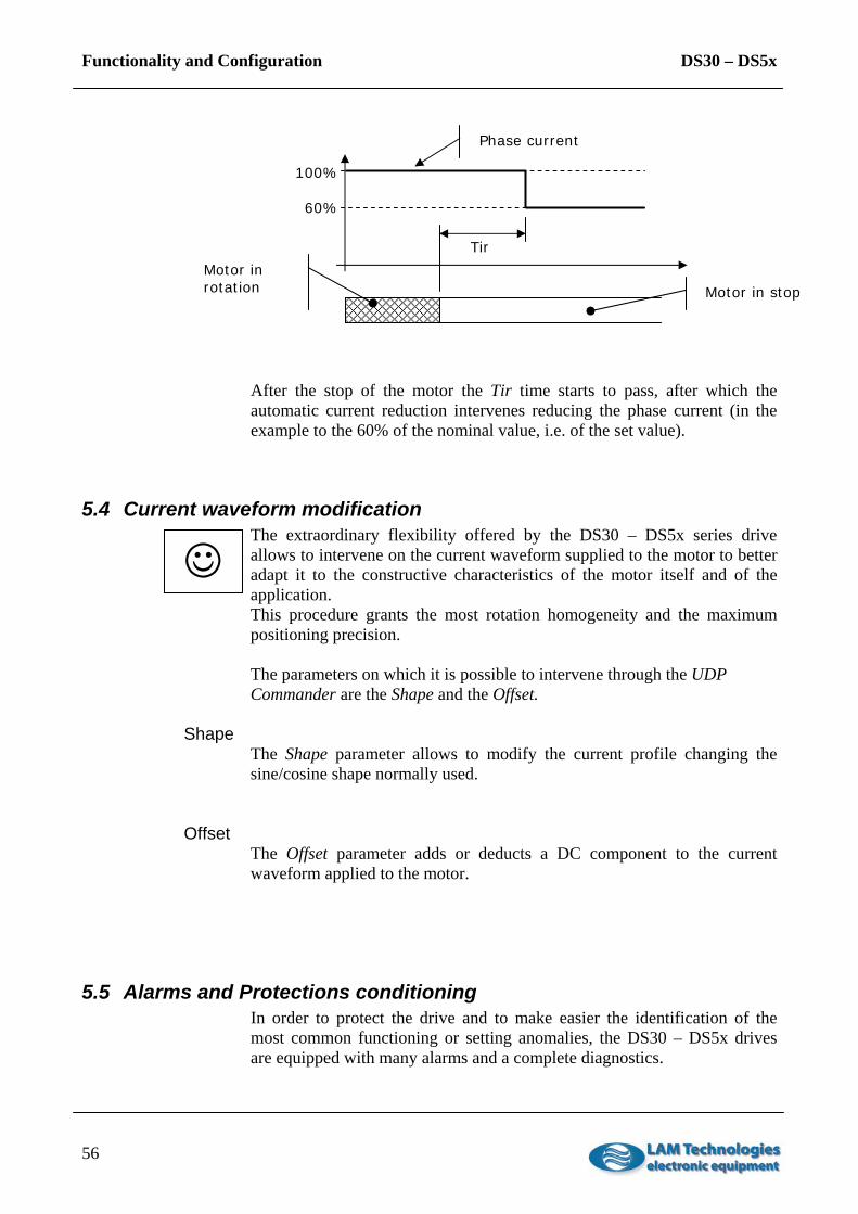
Functionality and Configuration DS30 – DS5x
56
After the stop of the motor the Tir time starts to pass, after which the automatic current reduction intervenes reducing the phase current (in the example to the 60% of the nominal value, i.e. of the set value).
5.4 Current waveform modification The extraordinary flexibility offered by the DS30 – DS5x series drive allows to intervene on the current waveform supplied to the motor to better adapt it to the constructive characteristics of the motor itself and of the application. This procedure grants the most rotation homogeneity and the maximum positioning precision. The parameters on which it is possible to intervene through the UDP Commander are the Shape and the Offset.
Shape The Shape parameter allows to modify the current profile changing the sine/cosine shape normally used.
Offset The Offset parameter adds or deducts a DC component to the current waveform applied to the motor.
5.5 Alarms and Protections conditioning In order to protect the drive and to make easier the identification of the most common functioning or setting anomalies, the DS30 – DS5x drives are equipped with many alarms and a complete diagnostics.
100%
60%
Tir
Phase current
Motor in stopMotor in rotation
DS30 – DS5x Functionality and Configuration
57
Furthermore, the extraordinary flexibility offered by the product allows to singularly configure the operative mode of each alarm choosing among Automatic, Permanent, Enable or Disable. The configuration is made without the necessity to intervene on the drive’s hardware, without jumper, dip-switch, etc.
Automatic The drive constantly examines the alarm condition and when this disappears it provides autonomously to remove the signal and to turn back to the operative status.
Permanent Each alarm condition remains in the drive’s memory. To remove the signal the drive must be switched off and then switched on again.
Enable The alarm condition signal remains till the drive is not disabled through the boolean ENABLE input.
Disable The alarms are disabled and ignored by the drive. For security reasons some protections cannot be put in this status. In the following table are resumed the various possible settings for each single alarm.
For a complete description of protections and alarms see chapter 5.7 Protections.
Alarm type / protection Possible setting Automatic Permanent Enable Disable
Under voltage Yes Yes Yes No Over voltage Yes Yes Yes No Over temperature Yes Yes Yes No Phase-to-phase short circuit Yes Yes Yes No Phase-to-ground short circuit (GND)
Yes Yes Yes No
Phase-Vp short circuit Yes Yes Yes No Interrupted Phase A Yes Yes Yes Yes Interrupted Phase B Yes Yes Yes Yes

Functionality and Configuration DS30 – DS5x
58
5.6 Signal LEDs The drive has three signal LEDs: the green one called On, the yellow LED called Enable / Run and the red one called Fault.
On The LED called On lights up when the drive is supplied with a voltage sufficient to allow a correct functioning of the control electronics. When the LED is on, the drive is able to elaborate the information but it is not necessarily in the working status (because, for examples, the supply voltage is beyond the working limits or the temperature is excessive).
Enable / Run This LED gives contemporaneously various information about the status of the drive. When the motor is enabled the LED is fixed lighted up, when the motor is disabled the LED is off. When the motor is rotating the LED status is inverted for a little while. In other words, when the motor is enabled and rotating this LED is mainly lighted up with short power-offs.
Fault
This LED lights up each time there is at least an alarm signaling. When the LED is lighted up, the drive is not operative and the motor is without supply (observe that also in this condition the yellow LED continues its own activity as described in the previous chapter). In presence of an alarm the red LED lights up and starts a sequence of flashing related to the kind of problem found. The following table shows the association between the number of flashes and the error found.
Relation between the yellow LED and the status of the motor Rotation Enable Yellow LED status
No No On Off
No Yes On Off
Yes No On Off
Yes Yes On Off

DS30 – DS5x Functionality and Configuration
59
If more than a problem occurs contemporaneously the lighting flashes sequences associated to each one of them are cyclically executed. If, for example, the over temperature condition occurs together with the over voltage one, the LED will flash twice and then three times alternatively till when the malfunction signaling will be removed. The drive features grant at least a visualization cycle for each activated alarm. For this reason it is not possible to remove an alarm before the first visualization cycle is finished. Observe that each error signals can be removed in different ways according to how the drive’s configuration has been made (for a close examination see chapter 5.5 Alarms and Protections conditioning). For a detailed description on the various alarms and protections see chapter 5.7 Protections. When in the drive the Loader (an always resident small software necessary for the firmware update) is active, the Fault LED remains always on. To restore the normal functioning it is sufficient to load a compatible firmware in the drive.
Codification of errors signaled by red LED Number of
flashes Problem description
1 Under voltage, the supply voltage is inferior to Vpl value 2 Over voltage, the supply voltage is superior to Vph value 3 Over temperature, the heat sink temperature is superior to Tchh 4 Phase-to-phase short circuit, one or two phases are in short circuit 5 Phase-to-ground short circuit (GND), phase in short circuit with ground 6 Phase-Vp short circuit, one phase is in short circuit with power supply 7 Interrupted phase A, connection between drive and motor is missing 8 Interrupted phase B, connection between drive and motor is missing

Functionality and Configuration DS30 – DS5x
60
5.7 Protections
5.7.1 General description The drive is equipped with efficient protections which protect its integrity whenever one of the most common problems occurs. Furthermore, some controls have been implemented which can detect positioning errors even before the motor starts to move. In spite of the care and attention used in the development and manufacturing of the drive, an installation or an use not in compliance with the indications present in this manual, or out of stated maximum limits, can damage the drive permanently. Through the configuration it is possible to define the drive behavior at the occurring of the various alarm conditions. For example, it is possible to choose and make permanent an alarm or to set the drive so that it is automatically re-enabled as soon the alarm condition is ceased. For a detailed description about the various configuration options see chapter 5.5 Alarms and Protections conditioning. When there is at least an alarm signal the drive is not active and the motor is not supplied, consequently the torque is null.
5.7.2 Under voltage The under voltage alarm intervenes when the drive supply voltage is inferior to the Vpl value (Vacl for the AC models). Such value varies according to the drive model as per the following table.
Model Vpl value (Vacl) Unit Min Typ Max
DSxx41 18
Vdc
DSxx44 20 DSxx48 20 DSxx73 24 DSxx76 24 DSxx78 24 DSxx84 45 DSxx87 45 DSxx98 45
DSxx41A 13.5
Vac
DSxx44A 15 DSxx48A 15 DSxx73A 18 DSxx76A 18 DSxx78A 18 DSxx84A 33 DSxx87A 33

DS30 – DS5x Functionality and Configuration
61
The drive constantly verifies the supply voltage value; it is sufficient that it goes beyond the Vpl threshold (Vacl for the AC models) for few instants to generate the under voltage alarm. It does not have to be astonishing the fact that the protection intervenes despite the measured voltage is within the functioning limits, as it is possible that, because of the main supply fluctuations or cables length, the voltage that effectively reaches the drive becomes, in particular moments (for example during the motor acceleration phase), inferior to Vpl value (Vacl for AC models). In order to make a correct measurement it is necessary to act directly on the drive supply terminal blocks, using a band-pass instrument of at least 10KHz (as an oscilloscope, for example) able to memorize the voltage transients minimum values. If the supply voltage is very near to the drive functioning limit and sporadically the under voltage alarm intervenes, it is possible, in some cases, to solve the problem reducing the distance between the power supply and the drive, increasing the cables section or placing an electrolytic capacitor near the drive itself (valid only the DC models).
Drive supply voltage
Vdc Vpl
t Under voltage protection intervention

Functionality and Configuration DS30 – DS5x
62
5.7.3 Over voltage The over voltage protection intervenes when the supply voltage is superior to the Vph value (Vach for the AC models). In these conditions the drive protects the power stage turning it off. Such value varies according to the drive model, as per the following table.
Model Vph value (Vach) Unit Min Typ Max
DSxx41 50
Vdc
DSxx44 55 DSxx48 55 DSxx73 98 DSxx76 98 DSxx78 98 DSxx84 175 DSxx87 175 DSxx98 248
DSxx41A 37
Vac
DSxx44A 40 DSxx48A 40 DSxx73A 71 DSxx76A 71 DSxx78A 71 DSxx84A 124 DSxx87A 124
The drive constantly controls the supply voltage and when it goes beyond the Vph value (Vach for AC models), even also for few instants, the over voltage protection intervenes. It does not have to be astonishing the fact that the protection intervenes despite the measured voltage is within drive functioning limits. In fact it is possible that, in some occasions (sudden motor decelerations, sudden voltage changes, etc.) the voltage which supplies the drive goes beyond the Vph value (Vach for AC models) causing the protection intervention. In order to make a correct measurement of the effective drive supply voltage it is necessary to act directly on the supply terminal blocks of the drive itself, using a band-pass instrument of at least 10KHz and able to capture the voltage transients peaks.

DS30 – DS5x Functionality and Configuration
63
If the supply voltage is very near to the drive functioning limit and the over voltage alarm sporadically intervenes, it is possible in some cases to solve the problem reducing the distance between the power supply and the drive, increasing the cables section or placing an electrolytic capacitor near the drive (valid only for DC models). ATTENTION, if the supply voltage increases a lot beyond the maximum functioning value, and in particular it goes beyond the Vpbrk breakdown voltage (Vacbrk for AC models), the drive will be irreversibly damaged. When the over voltage protection intervenes because of the energy returned from the motor during the deceleration phase, which causes a bus voltage rise beyond the Vph value (Vach for AC models), it is possible to avoid such condition using a braking resistor calibrated to intervene before the bus voltage reaches the Vph value (Vach for AC models). The power supplies of the DP1xx2 series integrate this functionality and represent a valid solution to solve this problem.
Over voltage protection intervention
Drive supply voltage Vdc Vph
t

Functionality and Configuration DS30 – DS5x
64
5.7.4 Over temperature The over temperature protection intervenes when the drive power stage temperature goes beyond the Tchh value. In this condition the drive stops working. This intervention ends when the temperature falls below Tchl value. When this occurs the alarm signal is removed or not according to the drive configuration (see chapter 5.5 Alarms and Protections conditioning).
Symbol Description Value Unit Min Typ Max
Tchh Intervention threshold of thermal protection 85 90 95 °C Tchl Restoration threshold of thermal protection 60 65 70 °C
5.7.5 Phase-to-phase short circuit In case of a motor wirings short circuit, on the same phase or on different phases (cross phase short circuit), the drive stops working and activates the phase-to-phase short circuit protection. This kind of protection requires a careful survey to find the cause of the short circuit. Consider that the short circuit can be, apart in the wiring, also inside the motor. According to the drive configuration (see chapter 5.5 Alarms and Protections conditioning) the protection can be removed through a turning off and on cycle or disabling temporarily the drive through the ENABLE signal.
Temperature Vdc Tchh Tchl
t
Intervention of thermal protection

DS30 – DS5x Functionality and Configuration
65
5.7.6 Phase-to-ground short circuit The protection starts whenever one of the connections towards the motor creates a short circuit with the drive ground connection (GND). In these conditions the drive protects itself switching off the supply to the motor and putting itself in an inactive status. This intervention of this protection requires a careful survey to find the cause of the short circuit. Consider that the short circuit can be, apart in the wiring, also inside the motor. According to the drive configuration (see chapter 5.5 Alarms and Protections conditioning) the protection can be removed through a turning off and on cycle or disabling temporarily the drive through the ENABLE signal.
5.7.7 Phase-to-Vp short circuit (Vac) Whenever one of the phase connections (motor connections) cause a short circuit with the supply voltage positive (+Vp or Vac for the AC models) the phase-to-Vp short circuit protection starts. When this condition occurs the drive protects itself switching off the supply to the motor and putting itself in an inactive status. According to the drive configuration (see chapter 5.5 Alarms and Protections conditioning) the protection can be removed through a turning off and on cycle or disabling temporarily the drive through the ENABLE signal.
5.7.8 Interrupted phase A, interrupted phase B If the connection between the drive and the motor is interrupted, even if of only a single phase, or an inner motor winding is damaged (interrupting itself), the drive activates the interrupted phase alarm. For a more accurate diagnostics the signal is distinguished for the phase A and phase B. Take present that the drive executes the interrupted phase control only with the drive enabled and with the motor at rest or with rotation speed inferior to 15rpm.

DS30 – DS5x Programming
67
6 Programming
6.1 Overview The DS30 – DS5x series drives allow to execute a program developed by the user driving the motor both in position and/or in speed mode. The programming is made putting in sequence more instruction blocks. An instruction block performs a specific function, as for example the variable assignment, a conditional jump, etc. To each instruction block can be given a reference label to be used as jump destination. At the beginning the drive executes in sequence the functional blocks, starting from the first one (block 001). The jump instruction blocks (jump or call) change the sequential program execution order. All the drive parameters and functions are controlled by the value present in a series of variables called system registers. The instruction blocks can read all the registers while only some of them can be written. For example the TargetPos register, which represents the motor final position, can be both read and written; while the bInPosition status boolean register, which indicates when the motor is in position, can be only read. Besides the system registers, the user can create one’s program variables defining their name and their size. Variables can be created 1-byte, 2-bytes, 3-bytes or 4-bytes long. The last types of available data are the constants or numbers. The constants can take any value included between -2,147,483,648 and 2,147,483,647. The firmware inside the drive is multitasking. The application program and the motion control algorithm are executed in two different tasks, this means that the eventual stop of the application program does not strictly cause a stop to the motor and vice versa. The application program is never suspended awaiting for the end of a movement; if the application has to wait for an event to continue, it is necessary to expressly insert a conditional jump or a wait until block. The entire application development takes place inside the UDP Commander software which assists the programmer from the writing of the application program, to its compiling, to the download of the compiled program into the drive until its test and debug. The drive connection is made through the DUP port. This connection allows to download the application program into the drive, to control its execution, to read the registers, the user variables, the I/O status, etc. Through the same port it is then possible to update the firmware inside the drive. This last feature deserves particular attention as it allows to maintain the product always updated.

Programming DS30 – DS5x
68
To connect the DUP port of the drive to the PC, it is necessary a little and cost-effective interface called UDP30. The UDP30 interface is connected to the PC through the USB port. To grant high noise immunity and to safeguard the equipment integrity, the connection between the PC and the drive must be of insulated-type. In addition, the UDP30 interface is able to supply the drive digital section, making possible the programming and the reading of the information therein contained even without the power supply. For a more detailed description on the features of the UDP30 interface please see the dedicate user’s manual.
6.2 Control hardware signals Through the control hardware signals the application program interacts with the external equipment.
The application program reads and/or changes the hardware signals through some specialized system registers. The I/O is updated in real time, therefore, writing 1 in the register associated to a digital output, the output itself is immediately activated. In the following tables are detailed the main characteristics of each signal and the associated system register.
Digital inputs
Number Voltage range
System register
Possible values
0 3..28Vdc DigitalInput(0) 0..1 1 3..28Vdc DigitalInput(1) 0..1 2 3..28Vdc DigitalInput(2) 0..1 3 3..28Vdc DigitalInput(3) 0..1
A digital input is defined active when it is supplied. When the input is in the active status, the corresponding system register assumes value 1. When the input is not active the register value is 0.
Digital outputs Number Voltage
range System register
Allowed values
0 1..30Vdc DigitalOutput(0) 0..1 1 1..30Vdc DigitalOutput(1) 0..1

DS30 – DS5x Programming
69
A digital output is active when it allows the current to flow. To activate an output the corresponding registers must be set to value 1. Setting a value equal to 0 the output is inactive. The drive is equipped with two analog bipolar inputs converted with resolution 10bit plus sign.
Analog inputs Number Voltage
range Input
impedanceSystem register
Possible values
0 -10..+10Vdc 47K AnalogInput(0) -1024..+1023 1 -10..+10Vdc 47K AnalogInput(1) -1024..+1023
The analog inputs have been designed to work also as digital inputs, in the need it is therefore possible to connect digital sources to the analog inputs. The voltage threshold used to discriminate the logic 1 from the logic 0 is freely adjustable from 1V to 10V through the configuration of the drive (see the UDP Commander user’s manual).
Analog inputs used as digital inputs Number Voltage
range Active input
treshold System register
Possible values
4 -28..28Vdc 1.5V DigitalInput(4) 0..1 5 -28..28Vdc 1.5V DigitalInput(5) 0..1
The analog output can also be used to supply little loads (as for example potenziometers, sensors, etc.) provided that the absorption is inferior to the current delivered by the output itself.
Analog outputs Number Voltage
range Output current
System register
Possible values
0 0..10Vdc 10mA AnalogOutput(0) 0..1023

Programming DS30 – DS5x
70
6.3 System registers The drive functionalities are controlled through the system registers. Some of them can be only read (R), others can be both read and written (RW). When trying to assign to a register a value out of the allowed range, the register is automatically clamped to the nearest maximum or minimum value. If trying to assign the value -35 to a register with range 0..100, then the register will assume the value 0; similarly trying to assign to the same register the value 122 the register will be set at a maximum value of 100.
The following table resumes the available registers.
Name Description Input /
Size Default Possible /
Allowed values Unit
RefVel Speed reference RW, 2bytes 0 -32768..+32767 0.25rpm Velocity Instantaneous speed R, 2bytes 0 -32768..+32767 0.25rpm TargetPos Target position RW, 4bytes 0 -2147483648…
+2147483647 1/128 step
Position Motor instantanous position RW, 4bytes 0 -2147483648… +2147483647
1/128 step
CPosition Seizing of the motor instantaneous position
RW, 4bytes 0 -2147483648… +2147483647
1/128 step
MaxVel Maximum rotation speed RW, 2bytes 2000 0..12000 0.25rpm Acceleration Allowed maximum acceleration RW, 2bytes 1000 1..30000 1rpm/s Deceleration Allowed maximum deceleration RW, 2bytes 1000 1..30000 1rpm/s ControlMode Movement control mode RW, 1byte 1 0..1 PhaseCurrent Motor phase current RW, 1byte I min Imin .. Imax 0.1Arms StByCurrent_Time Delay before current reduction RW, 1byte 5 1..100 100ms StByCurrent_Percentage Current reduction percentage RW, 1byte 50 0..100 % TimerA Timer RW, 2bytes 0 0..32767 1ms CounterA Counter RW, 2bytes 0 0..32767 Status Drive status R, 1byte -128..+127 ControlFlags It contains various control bits RW, 1byte 0 -128..+127 Fault Drive faults R, 1byte -128..+127 Error Drive errors R, 1byte -128..+127 bEnable Drive enabling RW, bool 0 0..1 bInPosition In position motor flag R, bool 0 0..1 bEnabled Drive enabling status R, bool 0 0..1 bInStop In stop motor flag R, bool 0 0..1 bUVarSaved Variables stored in flash R, bool 0 0..1 bUVarLoaded Variables loaded from flash R, bool 0 0..1 DigitalInput(0) 0 digital input image R, bool 0..1 DigitalInput(1) 1 digital input image R, bool 0..1 DigitalInput(2) 2 digital input image R, bool 0..1 DigitalInput(3) 3 digital input image R, bool 0..1 DigitalInput(4) 4 digital input image R, bool 0..1 DigitalInput(5) 5 digital input image R, bool 0..1 DigitalInputsA Digital inputs image R, 1byte -128..+127 DigitalOutput(0) 0 digital output image RW, bool 0 0..1 DigitalOutput(1) 1 digital output image RW, bool 0 0..1 DigitalOutputsA Digital outputs image R, 1byte -128..+127 AnalogInput(0) 0 analog input image R, 2bytes -1024..+1023 9.77mV AnalogInput(1) 1 analog input image R, 2bytes -1024..+1023 9.77mV AnalogOutput(0) 0 analog output image RW, 2bytes 0 0..1023 9.77mV
The DS30 – DS5x series contains an advanced motor control algorithm able to recalculate in real time the motor movement. This allows to change in any time the value of the movement control registers, without waiting for the motor to stop.

DS30 – DS5x Programming
71
6.3.1 Description of each single register The following is a detailed description of the various registers.
6.3.1.1 RefVel It is the speed reference used in the speed control mode (see ControlMode register description). When the drive works in position control mode, the content of the RefVel register is ignored. With the register set at 0 the motor stops, while at values different from 0 the motor rotates at a speed proportional to the absolute value of the register itself. The sign, positive or negative, of the value written in the RefVel register determines the rotation direction. In other words setting the RefVel register at the value -800 or +800, it is obtained an identical rotation speed, but in two different directions. The motor movement variations always occur according to the acceleration, deceleration and maximum speed values present in the Acceleration, Deceleration e MaxVel registers respectively. The RefVel register is accessible both in reading and in writing mode and can assume values between -32768 and +32767. Each unit corresponds to 0.25rpm, consequently setting for example the value 1000 in the MaxVel register, it is commanded a speed rotation of 250rpm.
6.3.1.2 Velocity It is useful to know the instantaneous speed of the motor. The value is constantly updated, wheather the drive works in position or in speed control mode. The Velocity is accessible on in reading. Each unit corresponds to 0.25rpm, consequently if the motor is rotating at a speed of 700rpm the Velocity register will contain the 2800 value.
6.3.1.3 TargetPos It represents the destination position of the motor, expressed in in 1/128 of full step, when the position control mode is selected (see ControlMode register description). When the drive works in speed control mode, the value of the TargetPos register is ignored. To command a positioning it is sufficient to write the destination quote value in the register. The motor will reach the target quote according to the values of acceleration, deceleration and maximum speed present in the Acceleration, Deceleration and MaxVel registers respectively. The TargetPos registers is accessible both in reading and in writing mode and can assume any value between -2,147,483,648 and +2,147,483,647.
6.3.1.4 Position Through this register it is possible to know the real time motor position expressed in 1/128 of step. The value is constantly updated whether the drive works in position or in speed control mode.

Programming DS30 – DS5x
72
The Position register, besides in reading, it is also accessible in writing and this allows to force the motor quote to any value. A typical case is the zero procedure where there is the need to put to 0 the motor quote, usually when the home sensor is activate. The Position register is accessible both in reading and in writing mode and can be set or assume values between -2,147,483,648 and +2,147,483,647.
6.3.1.5 CPosition In this register it can be stored the instantaneous position of the motor (Position register), espressed in 1/128 of step, when a predetermined digitial input is activate. The save operation of the motor position (also called capture) is very fast and it ends in a time inferior to 100us. Between one save and the following one there must be at least 2ms, otherwise the second save could not happen. The uses of the CPosition register are many and go from the products orientation, to the labelling, to the cutting “on the fly”, etc. The digital input which activates the storage is defined in the ControlFlags register (see further below). The CPosition register is accessibile both in reading and in writing and can be set or assume values bewten -2.147.483.648 and +2.147.483.647.
6.3.1.6 MaxVel The MaxVel register is useful to set the maximum speed limit at which the motor can rotate. The maximum speed value is an absolute value and it is applied for the movements executed by the motor in both directions. The speed constrainment occurs when the drive works both in position and in speed control mode. If the MaxVel register is dynamically modified with the motor in movement, the motor speed adjustment always occurs according to the acceleration and deceleration values present in the Acceleration and Deceleration registers respectively. The MaxVel register is accessible both in reading and in writing mode and it can assume values between 0 and +12000. Each unit corresponds to 0.25rpm, consequently setting for example the value 2000 in the MaxVel register the maximum speed is set at 500rpm.
6.3.1.7 Acceleration The motor acceleration is controlled by the Acceleration register and by the configuration of the drive (see the UDP Commander user’s manual) which allows to apply a multiplication factor equal to 4. It is possible to assign to the register values included between 1 and 30000 and it is allowed to change the value also with the motor in movement. The Acceleration register is accessible both in reading and in writing mode. Each unit corresponds to 1rpm/s, if in the configuration it is set a multiplication factor equal to 1, or 4rpm/s if it is set a multiplication factor equal to 4. For example, assigning the value 10000 to the Acceleration

DS30 – DS5x Programming
73
register it is set an acceleration equal to 10000rpm/s, with a multiplication factor x1, or 40000rpm/s with multiplication factor x4.
6.3.1.8 Deceleration The motor deceleration is controlled by the Deceleration register and by the configuration of the drive (see the UDP Commander user’s manual), which allows to apply a multiplication factor equal to 4. It is possible to assign to the register values included between 1 and 30000 and it is allowed to change the value also with the motor in movement. The Deceleration register is accessible both in reading and in writing mode. Each unit corresponds to 1rpm/s, if in the configuration it is set a multiplication factor equal to 1, or 4rpm/s if it is set a multiplication factor equal to 4. For example, assigning the value 4000 to the Deceleration register it is set a deceleration equal to 4000rpm/s, with a multiplication factor x1, or 16000rpm/s with multiplication factor x4.
6.3.1.9 ControlMode The ControlMode register allows to define the motor control mode. When the register value is 1 the drive works in speed control mode, while when the value is 0 the drive operates a position control. The register is accessible both in reading and in writing mode and it can be dynamically changed also during the movement. The following table resumes the possible values.
Value Description
0 Position control 1 Speed control
6.3.1.10 PhaseCurrent The contents of this register defines the effective current (Arms) supplied to the motor during the rotation. Each unit corresponds to 100mArms, therefore setting for example 35 in the PhaseCurrent register, the current supplied to the motor will be equal to 3.5Arms. The value of the register can be dynamically changed by the application program and this makes possible to adapt the motor torque to the various working phases reducing the current when the motor nominal torque is not necessary, or boosting the motor current if a greater torque is required for short times. The PhaseCurrent register is accessible both in reading and in writing mode. The minimum and maximum limit of the values writeable in the register is not fixed, but it varies according to the model of the drive. In the following table are listed the limits according to the model of the drive:

Programming DS30 – DS5x
74
6.3.1.11 StByCurrent_Time The StByCurrent_Time register allows to change the time expected, after the motor stop, before reducing the phase current. Each unit produces a delay of 100ms, therefore setting for example the register to the value 15, the motor phase current will be reduced after 1.5 seconds from stop. The StByCurrent_Time register is accessible both in reading and in writing mode and it can assume the values included between 1 and 100.
6.3.1.12 StByCurrent_Percentage It allows to define the phase current reduction percentage set through the PhaseCurrent register, passed the time from the motor stop defined in the StByCurrent_Time register. The StByCurrent_Percentage register is accessible both in reading and in writing mode and it can assume values included between 0 and 100.
6.3.1.13 TimerA The TimerA register has a particular characteristic. The value it contains is automatically decreased by the drive of one unit each msec until the 0 value is reached; such a value is maintained until the register is not written again. The register is normally used to realize delays or to measure the time between two events. The TimerA register is accessible both in reading and in writing mode and it can assume values included between 0 and 32767.
6.3.1.14 CounterA The 0 digital input ( DigitalInput(0) ) is associated to an hardware counter able to accept pulses up to a maximum frequency of 100KHz. The value of the counter is accessible through the CounterA register. The counter increase occurs during the active/inactive transition of the input, reached the value 32767 the count starts again from 0. To execute counts greater than 32767 it is possible to use the user variables and the programming tools to implement one exemption to the CounterA register. The hardware counter allows to realize many application as for example:
Model Minimum value
Maximum value
DSxx41(A) 3 14 DSxx44(A) 10 40 DSxx48(A) 30 80 DSxx73(A) 8 30 DSxx76(A) 20 60 DSxx78(A) 40 100 DSxx84(A) 20 40 DSxx87(A) 40 85
DSxx98 40 100

DS30 – DS5x Programming
75
• Closed loop systems. Counting the pulses received from an encoder or from a phonic wheel to verify the correct positioning of the motor.
• Execution of a positioning with ramp starting from a fixed frequency impulse train. Associating the counter value to the target position of the motor.
• Speed measurement of a master axis and consequent realization of an electrical axis. Verifying the number of pulses received within an unit of time.
• Electronic can. Using the counter value to assign the target position to the motor.
• Measurement of the wrapped/unwarapped film or tissue. Using an idler wheel moved by the film and connected to an encoder.
• Etc. The CounterA register is accessibile both in reading and in writing mode and can assume values included between 0 and 32767.
6.3.1.15 Status It is a read only register whose bits give various information about the status of the drive. The following table shows the correspondence between the bits and the given information.
Bit Name Description
bit7 bInPosition
It becomes active (value = 1) when the motor reaches the set position, i.e. when the Position register is equal to the TargetPos register
bit6 bInStop It becomes active (value = 1) when the motor is in stop state
bit5 bEnabled It becomes active (value = 1) when the motor is enabled
bit4 bFault It becomes active (value = 1) where there is at least one fault in the drive (Fault register <> 0)
bit3 bUVarLoaded Becomes active (value = 1) when the program variables are successfully loaded from flash memory
bit2 bUVarSaved Becomes active (value = 1) when the program variables are successfully saved to flash memory
bit3…bit0 Not used
Some bits are accessible also as Boolean-type independent registers.

Programming DS30 – DS5x
76
6.3.1.16 ControlFlags It is a register that controls some functions of the drive. The following table shows the correspondence between the various bits and the function performed.
Bit Name Description bit0 bEnable It allows to enable (value = 1) or disable
(value = 0) the motor. bit1 bit2 bit3
They allow to enable and define the digitial input used to store the motor quote (for more details see CPosition register) according to the following correspondence: bit3=0 bit2=0 bit1=0 disabled bit3=0 bit2=0 bit1=1 DI0 bit3=0 bit2=1 bit1=0 DI1 bit3=0 bit2=1 bit1=1 DI2 bit3=1 bit2=0 bit1=0 DI3
bit4..bit7 Not used
Some bits are accessible also as Boolean-type independent registers.
6.3.1.17 Fault It is a read only register which assumes a value different from 0 each time the drive detects a fault condition. The fault cause (or causes) can be easily determined analyzing the status of the various bits composing the register. The correspondence is resumed in the following table:
Bit Name Description bit7 It becomes active (value = 1) if the drive detects a
break phase condition on A phase. bit6 It becomes active (value = 1) if the drive detects a
break phase condition on B phase bit5 It becomes active (value = 1) when the drive detects a
short circuit between a phase and the Vp supply bit4 It becomes active (value = 1) when the drive detects a
short circuit between a phase and the supply negative (GND)
bit3 It becomes active (value = 1) when the drive detects a short circuit among the motor phases
bit2 It becomes active (value = 1) when the heat sink temperature exceeds the maximum allowed value
bit1 It becomes active (value = 1) when the power supply voltage exceeds the maximum allowed value
bit0 It becomes active (value = 1) when the power supply voltage is inferior to the minimum allowed value

DS30 – DS5x Programming
77
6.3.1.18 Error It is a read only register which assumes values different from 0 each time an error occurs inside the drive. In the following table are the possible values assumed by the register and their meaning:
Value Description
0 No error 1 Wrong application program checksum
6.3.1.19 bEnable It is a Boolean-type register useful to enable or disable the motor. When the value described in the register is 1 the motor is enabled, when the value is 0 the motor is disabled. The bEnable register is accessible both in reading and in writing mode. In the following table are resumed the effects produced by the various values assignable to the register:
Value Description 0 Disable the motor 1 Enable the motor
6.3.1.20 bInPosition It is a Boolean-type read only register which becomes active (value equal to 1) when the motor is in position. In other words the bInPosition register is activated when the value of the Position register is equal to the one present in the TargetPos register. This register is often used together with a conditional jump to suspend the application program execution until the motor has reached the position required. The bInPosition register is updated only when the position control mode is active. In the following table is resumed the meaning expressed by the various values:
Value Description 0 Motor not in position 1 Motor in position

Programming DS30 – DS5x
78
6.3.1.21 bInStop It is a Boolean-type read only register which becomes active (value equal to 1) when the motor is in stop. In the following table is resumed the meaning expressed in the various values:
Value Description
0 Motor in rotation 1 Motor in stop
6.3.1.22 bEnabled It is a Boolean-type read only register useful to know if the motor is enabled or not. In fact, the enable status does not depend only on the bEnable register, but also on the status of the drive. If, for example, there are fault conditions, the drive disables the motor independently from the value of the bEnable register. The purpose of the bEnabled register is to give information about the real status of the motor.
Value Description
0 Disabled motor 1 Enabled motor
6.3.1.23 bFault It is a Boolean-type read only register which becomes active (value equal to 1) when there is at least one fault in the drive (Fault register < > 0). In the following table is resumed the meaning expressed in the various values:
Value Description
0 Drive correctly working 1 Drive in fault
6.3.1.24 bUVarLoaded It is a Boolean-type read only register which becomes active (value equal to 1) when the program variables are successfully loaded from flash memory. Program variables are loaded from flash memory each time the program is reset and the flash memory contains a valid save, or whenever the variables are successfully saved to flash memory (see next section for details). The following table resumes the meaning according to the values:

DS30 – DS5x Programming
79
Value Description 0 Variables are initialized to the default
value 0 1 Variables are initialized with the values
read from flash memory
6.3.1.25 bUVarSaved It is a Boolean-type read only register which becomes active (value equal to 1) when the program variables are successfully stored in flash memory. If the save operation fails, the register is set as inactive (value is 0). The saving of the variables can automatically occur at shutdown if the corresponding option is selected in the configuration (see the UDP Commander user’s manual), or manually through the execution of a specific program block (for more information see par. 6.6.2.1 Save Variables in Flash). Note that the flash memory cannot be written for more than 50,000 times, and it is therefore necessary to limit the number of saves to this value. The following table resumes the meaning according to the values:
Value Description
0 Variables save not executed 1 Variables successfully saved to flash
memory
6.3.1.26 DigitalInput(0)..(3) It is a boolean-type read only register which reflects the status of the corresponding digital input. When the register assumes value 1 it means that the input is supplied (active); when the value of the register is 0 the input is disabled (inactive).
Value Description
0 Not supplied input (inactive) 1 Supplied input (active)
6.3.1.27 DigitalInput(4)..(5) It is a Boolean-type read only register which reflects the status of the analog input, when this is used to acquire digital signals. When the register assumes a value equal to 1 it means that to the input it is applied a voltage higher than 1.5V; when the value of the register is equal to 0 the voltage is lower than 1.5V.
Programming DS30 – DS5x
80
The DigitalInput(4) register corresponds to the 0 analog input, while the DigitalInput(5) register to the 1 analog input.
Value Description
0 Not supplied input (inactive) 1 Supplied input (active)
6.3.1.28 DigitalInputsA It is a read only register which includes the status of all the digital inputs (from DigitalInput(0) to DigitalInput(5) ). The correspondence between the bits and the inputs is the following:
Bit Name Description bit7..bit6 Not used
bit5 DigitalInput(5) 1 analog input used as in digital bit4 DigitalInput(4) 0 analog input used as in digital bit3 DigitalInput(3) 3 digital input bit2 DigitalInput(2) 2 digital input bit1 DigitalInput(1) 1 digital input bit0 DigitalInput(0) 0 digital input
When the bit assumes a value equal to 1, it means that the corresponding input is supplied (active); when the value of the register is equal to 0 the corresponding input is not supplied (inactive).
6.3.1.29 DigitalOutput(0)..(1) It is a Boolean-type register accessible both in reading and in writing mode. Setting the register to 1, the corresponding output is activated and it allows the current flow; on the contrary, setting the register to 0 the output is deactivated preventing the current flow.
6.3.1.30 DigitalOutputsA It is a register that includes the status of all the digital outputs ( DigitalOutput(0) and DigitalOutput(1) ). Modifying the status of one bit the corresponding digital output is changed. Setting the bit to 1 the output is activated; on the contrary, setting the bit to 0 the output is deactivated. The DigitalOutputsA register is accessibile both in reading and in writing mode.
Value Description 0 Inactive output 1 Active output

DS30 – DS5x Programming
81
The correspondence between the outputs and the bits of the register is the following:
Bit Name Description bit7..bit2 Not used
bit1 DigitalInput(1) 1 digital output bit0 DigitalInput(0) 0 digital output
6.3.1.31 AnalogInput(0)..(1) It is a read only register which reflects the status of the corresponding analog input. It can assume values included between -1024 and +1023 in correspondence with input voltage from -10V to +10V.
6.3.1.32 AnalogOutput(0) It is the register to be used to set the analog output voltage. It can be assigned to any value included between 0 and 1023. The AnalogOutput(0) register is accessible both in reading and in writing mode.
6.4 Variables Besides the registers, there are available program variables freely configurable by the user both as name and as size. The program variables are an essential resource to ensure the maximum flexibility and to allow to realize complex applications. The use of the variables allows to realize counters, for..next cycles, mathematic computations, etc. The variables are always signed integer-type and can represent both positive and negative integer numbers. The maximum value storable in the variable depends on the size of the variable itself which can be defined as of 1 byte, 2 bytes, 3 bytes or 4 bytes. In the following table are resumed the maximum and minimum values which can be stored in each variable size:
Size Access Allowed values
1 byte RW -128..+127 2 bytes RW -32768..+32767 3 bytes RW -8388608..+8388607 4 bytes RW -2147483648..+2147483647
If it is tried to assign a value greater than the maximum allowed one, the variable is automatically limited to the maximum or minimum allowed value. Through the drive configuration (see the UDP Commander user’s manual) you can set an autosave feature trigger at the drive shutdown able to make the variables retentive.
Programming DS30 – DS5x
82
It is also possible to manually save the variables through the execution of a specific program block (for more information see par. 6.6.2.1 Save Variables in Flash).
6.5 Constants The constants are represented by singed integer numbers. The constants can assume any value included between -2.147.483.648 and +2.147.483.647.
6.6 Instruction blocks The instruction block is the basic unit of the application program. An application program is built putting in sequence more instruction blocks. The UDP Commander software is a convenient graphic interface which assists the user during the writing of the application program. The following is a detailed description of the available instruction blocks:
6.6.1 Assignment The assignment block allows to give a value to a register or to a variable. The assignment can be either unconditional or conditional on the occurrence of a particular condition.
6.6.1.1 Unconditional The unconditional assignment is always performed and is composed of a left operand, that is the destination, and a right operand that is instead the source. Both of them can be registers and program variables, while only the operand on the right can also be a constant (a number) or a read only register. The following are some assignment examples:
Instruction block Description
Assign:
TargetPos = 1500 Position = 0
Assign to the TargetPos register the value 1500 and to the Position register the value 0
Assign:
DigitalOutput(0) = DigitalInput(1)
Put the 0 digital output in the same status of the 1 digital input
Assign:
myVar = Position Assign the value of the Position register to the myVar variable
Each block can contain up to 4 separate assignments. Assignments contained in the same block are processed without interruption and the value of the registers is guaranteed unchangeable throughout the execution of the block.

DS30 – DS5x Programming
83
6.6.1.2 Conditioning The conditioning assignment allows to assign a value to a register or to a variable only if the result of an expression is true. If the result is false the register or variable continue to maintain their value or take a second value declared as alternative (else case).
Instruction block Description
Assign: Position = 12800 if DigitalInput(3) = 1
Assign the value 12800 to the Position register if the digital input 3 is 1 (if the input is active)
Assign: RefVel = 1000 if AnalogInput(0) < 750 else
RefVel = 300
Assign the value 1000 to the RefVel register if the analog input 0 is less than 750 otherwise RefVel = 300
The entire block is processed without interruption and the value of the registers is guaranteed unchangeable throughout the execution of the block.
6.6.2 Function It is an instructions block that launches the execution of a specific function. Follows a detailed description of the available functions:
6.6.2.1 Save Variables in Flash This feature is useful to store the value of program variables in flash memory. The flash memory is able to maintain the stored data even in absence of power, and this allows to make the user variables retentive. Whenever variables are stored in flash memory the previous value is overwritten. Flash memory can be rewritten up to 50,000 times, and it is therefore necessary to respect this limit. The function is performed only when the motor is disabled (bit bEnabled equal to 0), otherwise the instruction block is ignored. When saving is finished, the function checks the integrity of data stored and if the operation is successful, the bUVarSaved bit is set active (value equal to 1). In this case, the variables are initialized with the values read from the flash memory and also the bit bUVarLoaded is set active (value equal to 1). If instead the writing operation fails, the bUVarSaved bit is placed inactive (value equal to 0). The variables in any case maintain their original value.
Instruction block Description
Function: Save Variables in Flash
Save the program variables in the flash memory (if bEnabled = 0)

Programming DS30 – DS5x
84
6.6.2.2 Reset User Program This feature is useful to reset the application program. The execution of this instruction block generates an immediate reset of the registers to their default values and the initialization of program variables to 0, or to the last value stored in flash, if available. In addition, the program execution resumes from the first block, exactly as it happens at drive startup.
Instruction block Description
Function: Reset User Program
Reset the application program.
6.6.3 Jump The jump instructions block allow to change the normal sequential execution flow of the application program. The jumps can be unconditional, which are always executed, or conditioned to the occurring of some particular condition. The jump destination is identified by a label; inside the program there must be one only instruction block with the same label. When the jump is executed, the application program execution changes instantaneously from the jump block to the block with the corresponding destination label. If the jump is a Call (call to a subroutine) it is possible to return to the program execution, from the instruction block successive to the one which has generated the jump, by inserting a Return instruction block. It must be observed that the reference to the return block is overwritten each time a Call jump is executed, therefore the Return instruction is always referred to the last Call executed
6.6.3.1 Unconditional jump An unconditional jump is simply coded by declaring the jump destination label. The following are some examples of unconditional jumps:
Instruction block Description
Jump to jumpHere always:
Jump always to the instruction block identified by the jumpHere label.
Call thisPlace always:
Jump always to the instruction block identified by the thisPlace label. If during the program execution it is met the Return instruction block, the program return to the instruction block successive to this one.

DS30 – DS5x Programming
85
6.6.3.2 Conditional jump The conditional jumps are characterized by two different operands and a comparison one. When the equation result is true the jump is executed, otherwise the drive executes the next instruction block. Both the right operand and the left one can be a register, a variable or a constant. Instead, the comparison operand must be chosen among the ones in the following table:
Operand Description
= The comparison is true when the operand value on the left is equal to the one on the right
<> The comparison is true when the operand value on the left is different from the one on the right
> The comparison is true when the operand value on the left is greater than the one on the right
>= The comparison is true when the operand value on the left is greater or equal to the one on the right
< The comparison is true when the operand value on the left is smaller than the one on the right
<= The comparison is true when the operand value on the left is smaller or equal to the one on the right
The following are some examples of conditional jump:
Instruction block Description
Jump to jumpHere if: Position > 12500
Jump to the instruction block identified by the jumpHere label if the value of the Position register is greater than 12500
Jump to startMovement if:
DigitalInput(0) = 1 Jump to the instruction block identified by the startMovement label if the value of the 0 digital input is 1 (if the input is active)
Call noElapse if:
TimerA <> 0 Jump to the instruction block identified by the noElapse label if the value of the TimerA register is different to 0. If during the program execution it is met the Return instruction block, the program return to the instruction block successive to this one.
Jump to doSomething if:
myVar1 <= myVar2 Jump to the instruction block identified by the doSomething label if the value of the myVar1 variable is smaller or equal to the value contained in the myVar2 variable

Programming DS30 – DS5x
86
6.6.4 Wait until The Wait unitl block has the purpose to suspend the execution of the applicative program until the specified condition becomes true. To define the condition there are two different operands and a comparison one. Both the right operand and the left one can be a register, a variable or a constant. Instead, the comparison operand must be chosen among the ones in the following table:
Operand Description = The comparison is true when the numeric operand
value on the left is equal to the one on the right <> The comparison is true when the numeric operand
value on the left is different to the one on the right > The comparison is true when the numeric operand
value on the left is greater than the one on the right >= The comparison is true when the numeric operand
value on the left is greater or equal to the one on the right
< The comparison is true when the numeric operand value on the left is smaller than the one on the right
<= The comparison is true when the numeri operand value on the left is smaller than the one on the right
The following are some examples of wait until:
Instruction block Description
Wait Until: Position > 51200
Suspend the execution of the application program until the poistion of the motor (Position register) has exceeded the value 51200
Wait Until:
DigitalInput(2) = 1 Suspend the execution of the application program until the 2 digital input becomes active
Wait Until:
bInPosition = 1 Suspend the execution of the application program until the motor has reached the trarget position
Considering that the Wait until block indefinitely suspends the execution of the program, it is suggested to use it only for event that will surely occur, otherwise it could block the application program. If a event time-out is needed, the TimerA must be used with the conditional jump.

DS30 – DS5x Programming
87
6.6.5 Delay It is an instruction block which suspend the execution of the application program for a predetermined time. The time is express in milliseconds and can be set as a numeric constant, a register or a variable. In these last two cases the delay will be equal to the value contained in the register or in the variable. The range can vary from 0 to 32000ms (equal to 32s). Setting greater or smaller values the delay is in any case limited bewteen 0 and 32000ms. The following are some examples of the Delay instruction block:
Instruction block Description
Wait for 1250 ms
Suspend the execution of the application program for 1250 ms (i.e. for 1.25 seconds)
Wait for AnalogInput(0) ms
Suspend the execution of the application program for the milliseconds corresponding to the voltage applied to the 0 analog input
Wait for myVar ms
Suspend the execution of the application program for the number of milliseconds contained in the myVar variable

Programming DS30 – DS5x
88
6.6.6 Return The Return instruction block has the task to turn back the execution of the program to the instruction block subsequent to the last one which executed a Call jump. If the Return instruction block is met in absence of a Call jump, the execution return to the first instruction block of the application program (block 001). It must be observed that the refence to the return block is overwritten each time a Call jump is executed, therefore the Return instruction is always referred to the last Call executed. The Return instruction block can also be used to “force” a return block specifying its label. The following are some examples of the Return instruction block:
Instruction block Description
Return
The execution of the application program returns to the bloch subsequent to the block which has executed the last Call
Set return address to here
Set the block identified by the here label as the instruction block which will be executed immediately after the execution of the Return block

DS30 – DS5x Programming
89
6.6.7 Mathematics
The mathematic instruction block is a powerful instrument which is rarely present in drives belonging to this price range. The block resolves the following equation
(m1 x m2)
result = -------------- + c bd The result operand on the left can be a variable or a register which has the writing access. The m1, m2 and c operands can be indifferently variables, registers or constants. The bd division coefficient can be chosen among the powers of 2 included between 2^0 and 2^30. Thanks to the denominator it is possible to simulate computations with decimal coefficients. If, for example, it was necessary to multiply a value by 1.5, it is possible to obtain an identical result multiplying first by 3 and then dividing by 2 (2^1). Choosing the correct multiplier/divisor combination it is possible to approximate any decimal multiplication or division. The following are some examples of mathematic instruction block:
Instruction block Description
Resolve:
TargetPos = 10 * AnalogInput(0)
The TargetPos register is set to 10 times the value assumed by the 0 analog input
Resolve:
counter = counter + 1
The counter variable is increased by one unit
Resolve: MaxVel = (DigitalInput(2) *
1000) + 500
The MaxVel register assumes value 500 when the 2 digital input is inactive (value = 0) and 1500 when the 2 input is active (value = 1)
Resolve:
myVar = (3 * myVar) / 8
The value contained in the myVar variable is multiplied by a 0.375 (3/8) factor
The mathematic block has an execution time longer than the other functional blocks, therefore when a fast reaction is required (less than 1ms) it is better to execute before the computations, storing the result in a temporary variable.

Programming DS30 – DS5x
90
6.6.8 Logic operations
The logic operation block allows to handle bits of registers or variables. Besides the usual operations in AND, OR and XOR it is possible to execute the SHIFT to right or left. In the shift operation all the outgoing bits are lost while the new bits are put to 0.
result = (op1 fnc1 op2) fnc2 op3
The result operand on the left can be a variable or register which has the writing access. The op1, op2 and op3 operand can be indifferently variables, registers or constants. The fnc1 and fnc2 logic functions must be chosen among the following ones:
Operand Description AND Execute the AND bit by bit. The result is 1 if both bit
compared are 1, otherwise the result is 0. OR Execute the OR bit by bit. The result is 1 if at least one
of the two bit compated is 1, otherwise the result is 0. XOR Execute the XOR bit by bit. The result is 1 if one of the
two bits compared is 1 and the other 0, otherwise the result is 0 if both bits are equal.
SHIFT_R Execute the shift to right of the operand on the left for the number of bits specified in the operand in the right. At any shift the less significant bit (lsb) is lost and the more significant bit (msb) is put to 0.
SHIFT_L Execute the shift to left of the operand on the left for the number of bits specified in the operand on the right. At any shift the more significant bit (msb) is lost and the less significant bit (lsb) is put to 0.
The following are some example of the logic operations block:
Instruction block Description
Resolve:
DigitalOutputsA = DigitalOutputsA XOR 3
The DigitalOutput(0) and DigitalOutput(1) digital outputs are inverted (if the output was active it becomes inactive and vice versa).
Resolve: myVar = (myVar AND 0xF3)
OR 128
The bit2 and bit3 of the myVar variable are put to 0 and the bit7 is put to 1. It must be observed that the numeric constants can be also written in hexadecimal format.
Resolve:
myVar = DigitalInputsA SHIFT_R 3
The bit2, bit1 and bit0 of the myVar variable are assigned respectively to the DigitalInput(5), DigitalInput(4) e DigitalInput(3) digital inputs.

DS30 – DS5x Programming
91
6.7 Common programming construct During the writing of an application program some recurrent instruction blocks combinations are often met. The following are the examples of the most common ones:
6.7.1 Loop This construct is very frequently used. Each application program has at least an infinite loop cycle: the main loop. The main loop of the program is used to transfer the control from the last instruction block again to the first one for a successive processing. Without a main loop, the application program would end after the execution of the last instruction block.
Instruction block Description startLoop: …:
…
First block of the loop. The startLoop label is used as input reference to the block
…:
…
Instruction blocks inside the loop
Jump to startLoop always:
Unconditional jump which returns the execution of the program to the beginning of the loop

Programming DS30 – DS5x
92
6.7.2 Delay without suspend program execution When there is the need to realize a wait and it is possible to suspend the execution of the program, it is possible to use the Delay block (for more information see par. 6.6.4 Wait until). If on the contrary during the wait the application program must continue to process the instruction blocks (for example to control an error condition or a wait cancellation) it is possible to use the TimerA to realize an untriggered wait.
Instruction block Description
Assign:
TimerA = 80 It is assigned to the TimerA register the time to be waited (80ms)
waitHere: …:
…
First block of the loop executed during the wait
…:
…
Further instruction blocks inside the wait loop
Jump to waitHere if:
TimerA <> 0 Jump to the waitHere label until the value of the TimerA register (automatically decreased) reaches the 0 value

DS30 – DS5x Programming
93
6.7.3 For .. Next cycle The For..Next cycles are useful to execute one or more instruction blocks for a well defined number of times. It is assumed that the forNextCnt variable is already declared with a length equal to 2 bytes. The following example is valid for cycles repeated at least one time.
Instruction block Description
Assign: forNextCnt = 1450
It is assigned to the variable used as counter the number of cycles to be execute (1450)
startFor: …:
…
First for..next cycle block. The startFor label is used as block reference
…:
…
Instruction blocks inside the for..next cycle
Resolve: forNextCnt = forNextCnt - 1
The forNextCnt variable is decreased by one unit
Jump to startFor if:
forNextCnt <> 0 Jump to the instruction block identified by the startFor label (for..next cycle start) if the value of the forNextCnt variable is different from 0
…:
…
First block executed after the for..next cycle is completed (forNextCnt variable = 0)

Programming DS30 – DS5x
94
6.7.4 If …Then…Else Whenever it is necessary to perform an operation conditioned to the occurring of determined conditions, it is used the If..Then construct; if it is then necessary to execute a second operation, in the case the required condition is not satisfied, it is used the Else structure.
Instruction block Description
Jump to hereIfTrue if:
Position > 18000
Jump to the instruction block identified by the hereIfTrue label if the value of the Position register is greater than 18000
…:
…
First executed block if the condition is false. This represents the first block of the Else case
…:
…
Instruction blocks of the Else case
Jump to nextOperation always:
Unconditional jump which terminates the blocks of the Else case and transfers the execution of the program to the first following block to the If…Then…Else construct
hereIfTrue: …:
…
First block executed if the condition is true. This represents the first block of the Then case
…:
…
Instruction blocks of the Then case
nextOperation: …:
…
First block subsequent to the If…Then…Else construct executed independently from the test result

DS30 – DS5x Programming
95
6.7.5 Hysteresis When analog values are used it is often necessary to condition the signal with an hysteresis to avoid that continuous little signal fluctuations (often due to electric noise) produce on the application undesired effects. To better comprehend this problem, it can be taken as an example the use of an analog input to command the motor position. Because of the electrical noise the A/D converted value oscillates of some units around the medium value; if the converted number is used directly as destination position, the motor will continuously move around the medium position. This may cause mechanical stress and noises and the not intervention of the current reduction function (which occurs only if the motor is in stop). To avoid this behavior it is sufficient to insert a simple algorithm which realizes an hysteresis on the analog input signal. The following example realizes an hysteresis of +/-3 units in respect to the value read by the analog input. It is assumed that the myVar, hystHigh and hystLow variables are already declared with a length equal to 2 bytes.
Instruction block Description readAgain: Assign:
myVar = AnalogInput(0)
Assign the real time value of the 0 analog input to the myVar program variable
Jump to outOfHyst if:
myVar > hystHigh
If the myVar variable is greater than the hysteresis higher limit (hystHigh variable) it is updated the hysteresis limits and carried out the required operations
Jump to readAgain if:
myVar >= hystLow
This block is reached only if the myVar variable is smaller or equal to the hysteresis positive limit. Now it is controlled if the myVar variable is smaller than the hysteresis lower limit (hystLow variable), in this case it is updated the hysteresis limits and carried out the required operations. It must be noted that the test is negate to avoid the unconditional jump block that would be necessary to return to the readAgain label
outOfHyst: Resolve:
hystLow = myVar - 3
It is updated the hysteresis negative limit with a value 3 units lower than the myVar variable (that corresponds to the reading of the analog input)
Resolve:
hystHigh = myVar + 3
It is updated the hysteresis positive limit with a value 3 units higher than the myVar variable (that corresponds to the reading of the analog input)
…:
…
Other operations to execute…

Programming DS30 – DS5x
96
6.7.6 Constraint of a value The shown algorithm is used to contain a value between a minimum and a maximum one. In the example it is assumed to associate the analog output of the drive to an analog input, with the constraint that the analog output reproduces input variations included only between 1Vdc and 5Vdc. It must be noted that these voltages are equivalent to a numeric value converted by the A/D of 102 and 512 respectively. It is assumed that the myVar variable is already declared with a length equal to 2 bytes.
Instruction block Description
readAgain: Assign:
myVar = AnalogInput(0)
Assign the real time value of the 0 analog input to the myVar program variable
Jump to checkHigh if:
myVar >= 102
If the myVar variable is higher or equal to the allowed minimum one, jump to the instruction block for the maximum limit control
Assign:
myVar = 102
This block is reached if the value of the myVar variable is lower than the allowed minimum one. In this case the minimum value is assigned
Jump to upDateAO always:
Unconditional jump to the analog output update block
checkHigh: Jump to upDateAO if:
myVar <= 512
This block is reached only if the myVar variable is higher or equal to the allowed minimum one. Now it is controlled if the myVar variable is lower than the maximum limit, in this case jump to the analog output update block
Assign:
myVar = 512
This block is reached if the value of the myVar variable is higher than the allowed maximum one. In this case the maximum value is assigned
upDateAO: Assign:
AnalogOutput(0) = myVar
Update the analog output with the value clipped between 102 and 512
Jump to readAgain always:
Unconditional jump that returns the program execution to the readAgain label
DS30 – DS5x Programming
97
6.7.7 CounterA extension on 32bits The CounterA counts the pulses applied to the DI0 input, reached the maximum value of 32767 the counter starts again from 0. In some application it could be necessary to have a wider counting capacity. The following example extends the CounterA register to 32bits to count up to 2147483647 pulses. It is assumed that the savedCounterA, oldCounterA and cntPulse variables, are already declared with a length equal to 2 bytes and the new32CounterA variable with a length of 4 bytes.
Instruction block Description
Assign: savedCounterA = CounterA
Store the value of the counter in the saveCounterA variable as the CounterA register can change during the successive processing (because of the pulses applied to the DI0 input)
Jump to calc if:
savedCounterA >= oldCounterA
If the counter has not executed the rollover (i.e. it has not reached 32767 and started again from 0) jump to the instruction block identified by the calc label
Resolve: cntPulse = (-1 * oldCounterA
) + 32768
This block is reached if the counter has started again from 0 (rollover). Execute the difference between 32768 and the previous value of the counter to calculate how many counts are to arrive to 0
Resolve:
cntPulse = cntPulse + saveCounterA
Add the counts executed after the rollover
Jump to acc always:
Unconditional jump to the block identified by the acc label
calc: Resolve: cntPulse = (-1 * oldCounterA
) + saveCounterA
Execute the difference between the currently value of the counter and the previous value saved to obtain the total number of pulses counted in the previous processing
acc: Resolve:
new32CounterA = new32CounterA + cntPulse
Add to the new32CounterA the pulses counted in the previous processing
Assign:
oldCounterA = savedCounterA
Update the oldCounterA variable for the successive processing

Fieldbus DS30 – DS5x
98
7 Fieldbus The information contained in the following chapters apply only to the drives provided with fieldbus, belonging to the DS5x series. The DS30 products are not supplied with fieldbus.
7.1 General description Through the fieldbus it is possible to access to the drive registers and to the program variables to monitor or control the status of the motor. The ability of the drive to execute an own internal program and to communicate contemporaneously with an external device (PC, PLC, CNC, etc.) offers a great flexibility and infinite applicative possibilities. The machine cycle can, for example, be implemented inside the drive, to obtain execution rapidity, and parametrized by the control master (for example in the times, in the repetition numbers, in the quotes or speeds of the motor, etc.), also with the motor in rotation! A further advantage offered by this kind of approach is to enormously limit the number of messages passing on the bus. Inside a structure with decentralized intelligence it is in fact sufficient to send only once the configuration parameters, to command the start and eventually to interrogate once in a while the drive to know its status. The various I/O of the drive (both analog and digital) allow to locally control the sensors such as end-run, home, load cells, resistors, etc., as well as actuators like electromagnets, proportional valves, etc., furtherly relieving the control master of the working load and improving the real-time reply of the system.
7.2 Modbus-RTU communication protocol The communication protocol implemented in the drives belonging to the DS5x series is the industrial standard Modbus-RTU. The Modbus protocol, born in 1979, soon imposed itself as a standard in the industrial field. Appreciated for its simplicity and efficiency, it is a free protocol which does not require the payment of royalties to be implemented or used. Despite the inferior communication speed in comparison to other protocols (such as Profibus and CAN), it vaunts a great number of installation, constantly increasing, as it represents a simple and economic solution to realize nets and undernets on the machine. It must not be confused the communication protocol with the physical mean used for data conveyance (called also layer). The protocol (in our case the Modbus-RTU) is the “language” used by the devices to “speak” to each other while the communication mean can be different (RS485, optical fibre, current loop, etc.).

DS30 – DS5x Fieldbus
99
For example, it is possible to communicate in Spanish by phone, fax, e-mail, etc. The phone, the fax, etc. are the physical mean (the layer) while the Spanish grammar is the protocol. The DS5x series drives are available in 3 different physical layers as detailed in the following table:
Model Physical Layer Notes DS50xx(A) RS485 It allows to connect more devices to a same
communication bus. Optimum noise immunity. Maximum distance 1000m
DS52xx(A) RS232 Suitable for point-to-point connections. Maximum distance between the devices 20m
DS54xx(A) USB Through the Hub it is possible to connect more drives to a same PC. Maximum distance between the PC (or the Hub) and the drive 5m
The Modbus-RTU protocol strictly provides for a master-slave relation. In the net there is always one only master and one or more slave devices. Each communication is always generated by the master. The slave can send data only further to a command or an inquiry sent by the master. The master device (PC, PLC, etc) identifies the slave with which to communicate through an address which must be univocal inside the net. In other words each slave must have an address different from all the others. The possible addresses vary from 1 to 247. The special address 0 has the function of broadcast address, i.e. it allows to send a command which will be processed contemporaneously by all the devices in the net. The use of the address 0 does not provide any reply by the slaves. The set of data which compose a Modbus-RTU command includes, besides the slave device address, also a function code, a group of data depending on the function invoked and at last a checksum useful to evaluate the integrity of the received data. In the following description the number in hexadecimal notation are anticipated by the suffix “0x”. The value 0x22 for example indicates the hexadecimal number 22 which corresponds to the value 34 in the decimal notation. A detailed description of the Modbus-RTU communication goes beyond the purpose of the this manual. Following are detailed only some basic notions to help and better comprehend the functioning of the product. For an exhaustive description of the Modbus protocol see the official documentation on the site www.modbus.org.

Fieldbus DS30 – DS5x
100
7.2.1 Data structure (frame) The set of data (called frame) which pass from the master control device (PC, PLC or else) towards the slave (the drive for example) and vice versa is always organized in the same way and satisfies the following structure:
Address Function Code Data CRC Address, it is the address of the slave receiver of the command when the data flow is from the master towards the slave, or the address of the slave which transmits when the data flow is from the slave to the master (reply). Function Code, it identifies the function the master wants the slave to execute when the data flow is from the master towards the slave, or the function elaborated by the slave when the data flow is from the slave to the master (reply). Data, specific information about the evoked function, transmitted to the slave or received by the same. CRC, it is the checksum calculated by the sender using all the data of the frame. The receiver then calculates the CRC of the received data and compares it with the CRC received.
7.2.2 Data processing (frame) The slave device processes the data which follow the address only if the address itself corresponds to its own or to the address 0 (broadcast address). In all the other cases the data which follow the address are ignored. Once recognized the address, the slave memorizes all the remaining data until it receives the CRC and then calculates the CRC using the received data and compares it with the received CRC. If the two values are different, the slave ignores the frame and keeps listening again without sending any reply. The master device detects this condition as transmission time-out (lack of reply from the slave). If the CRC is correct the slave tries to execute the command given by the master and if the operation successfully ends the slave sends the appropriate reply to the master (according to the Function Code or no reply if the address was 0, i.e. broadcast address). In the case the slave cannot execute the command given by the master, it sends an error reply called Exception Frame composed as follows:
Address Function Code OR 0x80 Exception Code CRC Address, it is the address of the slave which sends the reply.

DS30 – DS5x Fieldbus
101
Function Code OR 0x80, it is the code of the function which has generated the error with the bit7 (the most significant bit or MSB) set to 1 (it is equivalent to make the OR of the function code with the value 0x80). Exception Code, it is a code which gives an indication about the type of problem detected by the slave. CRC, it is the checksum calculated by the slave. The possible transmitted Exception Codes are the following:
Exception Code Description 0x01 It indicates that it is not possible to execute the required function.
Possible causes are the not implementation of the same function, an attempt to write onto an only writing location, etc.
0x02 It indicates that the location to which there is an attempt to access does not exist.
0x03 It indicates that one or more values are beyond the allowed limits.
7.2.3 Checksum computation (CRC) The checksum computation (CRC) examines the whole frame (with the exception of the CRC which is instead calculated). The CRC has the size of a word (2bytes) and is calculated applying the following algorithm to any byte of the frame.
1. The CRC is initialized to the value 0xFFFF. 2. It is executed the XOR (OR exclusive) of the byte with the low byte
of the CRC, memorizing the result of the CRC. 3. It is executed the shift (rotation) of the CRC of a position (one bit)
towards right and it is set to 0 the bit15 (MSB) of the CRC 4. If the bit0 (LSB) before the shift was 0 it return to the point 3,
while if the bit0 (LSB) before the shift was at 1 it is executed the XOR of the CRC with the value 0xA001.
5. The points 3 and 4 must be repeated 8 times for each byte (8 shifts). 6. It is repeated from point 2 until all the frame bytes are processed. 7. The CRC value is the checksum.
It must be considered that the checksum is transmitted in reverse order in respect to the other words. The first byte transmitted is the less significant one and the second byte transmitted is the most significant byte. Inside the frame the CRC is therefore disposed as follows:
CRC Lo
CRC Hi

Fieldbus DS30 – DS5x
102
7.2.4 Data organization Inside the drive there are 5 different types of data with different dimensions; bit, byte, word (2 bytes), 3byte, and dword (double word i.e. 4 bytes). Any register or program variable, read or written through the Modubus-RTU protocol must been formatted inside one or more words. Following are detailed the rules with which the data in the various dimensions are or must be formatted and interpreted:
7.2.4.1 bit The binary-type data corresponds to the bit0 of the word. The other bits, from bit1 to bit15, remain unused and have value 0. Es. 1 bit=0
Word 0 bit15 bit0
0 0 0 0 0 0 0 0 0 0 0 0 0 0 0 0 Es. 2 bit=1
Word 0 bit15 bit0
0 0 0 0 0 0 0 0 0 0 0 0 0 0 0 1
7.2.4.2 byte The byte-type data are present in the lowest 8 bits of the word (from bit7 to bit0), the higher 8 bits (from bit15 to bit8) are instead set to 1 or 0 following the rule of the extension of the sign; if the byte value is >= 0 the bits are set to 0, if instead it is < 0 the are all set to 1. Es. 1 byte = 58 (0x3A)
Word 0 bit15 bit0
0 0 0 0 0 0 0 0 0 0 1 1 1 0 1 0
Bit value
Bit value

DS30 – DS5x Fieldbus
103
Sign extension Byte value (58) Es. 2 byte = -61 (0xC3)
Word 0 bit15 bit0
1 1 1 1 1 1 1 1 1 1 0 0 0 0 1 1
Sign extension Byte value (-61)
7.2.4.3 word The word-type data are represented in native mode, without any particular format. Es. 1 word = 12384 (0x3060)
Word 0 bit15 bit0
0 0 1 1 0 0 0 0 0 1 1 0 0 0 0 0
Word value (0x3060) Es. 2 byte = -3172 (0xF39C)
Word 0 bit15 bit0
1 1 1 1 0 0 1 1 1 0 0 1 1 1 0 0
Word value (0xF39C)
7.2.4.4 3byte The 3bytes data are represented using two words. The first word, the one with minor address, contains in the lowest 8 bits (from bit7 to bit0) the most significant byte of the data while the superior 8 bits (from bit15 to bit8) are set to 1 or 0 following the rule of the extension of the sign; if the byte value is >= 0 the bits are set to 0, if instead it is < 0 they are all set to

Fieldbus DS30 – DS5x
104
1. The second word, with address + 1, contains the two remaining bytes of the data. Es. 1 3byte = 1526317 (0x174A2D)
Word 0 bit15 bit0
0 0 0 0 0 0 0 0 0 0 0 1 0 1 1 1
Sign extension The most significant byte (0x17)
Word 1
bit15 bit0 0 1 0 0 1 0 1 0 0 0 1 0 1 1 0 1
Rmaining 2 bytes (0x4A2D)
Es. 2 3byte = -1270301 (0xEC9DE3)
Word 0 bit15 bit0
1 1 1 1 1 1 1 1 1 1 1 0 1 1 0 0
Sign extension The most significant byte (0xEC)
Word 1
bit15 bit0 1 0 0 1 1 1 0 1 1 1 1 0 0 0 1 1
Remaining 2 bytes (0x9DE3)

DS30 – DS5x Fieldbus
105
7.2.4.5 dword The dword-type data are represented using two words. The first word, the one with the minor ID (address), contains the two most significant bytes of the dword while the second word with address + 1, contains the two remaining bytes of the dword. Es. 1 word = 898271058 (0x358A8752)
Word 0 bit15 bit0
0 0 1 1 0 1 0 1 1 0 0 0 1 0 1 0
Value of the most signigicant bytes (0x358A)
Word 1
bit15 bit0 1 0 0 0 0 1 1 1 0 1 0 1 0 0 1 0
Value of the two most significant bytes (0x8752) Es. 2 word = -1026521534 (0xC2D08642)
Word 0 bit15 bit0
1 1 0 0 0 0 1 0 1 1 0 1 0 0 0 0
Value of the two most significant bytes (0xC2D0)
Word 1 bit15 bit0
1 0 0 0 0 1 1 0 0 1 0 0 0 0 1 0
Value of the two most significant bytes (0x8642)

Fieldbus DS30 – DS5x
106
7.2.5 Supported functions The manipulation of each register or program variable is executed using only three standard functions of the Modbus protocol. The function with code 0x03 is useful to read the registers or the variables and allows to contemporaneously read up to 2 words at the time. The function 0x10 instead is useful to write both registers and variables and allows to write up to 2 words at the time. Finally, the function with code 0x16 allows to change only some bits of a register or a variable leaving the remaining bits unchanged.
7.2.5.1 0x03, Reading of registers and variables (Read Holding Registers) The command is useful to read the registers or the program variables. Through the parameter Word Number it is possible to choose if reading one only word or two words contemporaneously. This last mode is useful to read registers or variables with a dimension of 3 or 4 bytes. The following table shows the composition of the frame transmitted to the drive and the relative reply in case of command successfully concluded.
Function 0x03, Read Holding Registers Request (Master Slave)
TransmittedFrame structure
Address Function Code
Word ID Word Number
CRC
Dimension (byte) 1 1 2 2 2 Possible values 1..247 0x03 0..655351 1 or 2 0..65535
Reply (Slave Master)Received
Frame structureAddress Function
Code Byte
Counter Word0 Value
[Word1 Value]
CRC
Dimension (byte) 1 1 1 2 2 2 Possible values 1..247 0x03 2 or 4 0..65535 0..65535 0..65535
Address, it is the address of the slave receiver of the command when the data flow is from the master towards the slave or the address of the slave which transmits when the data flow is from the slave to the master (reply). Function code, it is the identification of the function for the reading of registers and program variables (0x03). Word ID, it is the ID (also called address) of the first word to which to access.
1 Only some addresses correspond to valid registers and variables (see further on). The access to non-existent registers or variables produces an error reply message from the drive.

DS30 – DS5x Fieldbus
107
Word number, it is the quantity of words on which to operate. At most it is possible to operate on 2 words at the time. Byte counter, it contains the number of bytes which will follow excepted the CRC. Its value is the double of the Word Number parameter. Word0 value, it is the value of the first read word corresponding to the Word ID. Word1 Value, it is the value of the second read word relative to the Word ID + 1. The parameter is indicated between square brackets because it is present only when the command is sent with Word Number = 2. Differently the Word1 Value is not received. CRC, it is the checksum calculated by the sender using all the frame data. The receiver calculates the CRC of the received data and compares it with the CRC received.
Ex. 1, reading of the register 41226 (Acceleration) from the drive with address 1
Function 0x03, Read Holding Registers Request (Master Slave)
Transmitted frame structure
Address Function Code
Word ID Word Number
CRC
Transmitted values 0x01 0x03 0xA109 0x0001 0x77F4 Replay (Slave Master)
Received frame structure
Address Function Code
Byte Counter
Word0 Value
[Word1 Value]
CRC
Received values 0x01 0x03 0x02 0x03E82 0xB8FA
2 The value changes according to the real content of the register

Fieldbus DS30 – DS5x
108
7.2.5.2 0x10, Writing of registers and variables (Write Multiple Registers) The command is useful to write the records or the program variables. Through the Word Number parameter it is possible to choose to write one only word or two words contemporaneously. This last mode is useful to write registers or variables with a size of 3 or 4 bytes. The following table shows the composition of the frame transmitted to the drive and of the relative reply in case of command successfully concluded.
Function 0x10, Write Multiple Registers Request (Master Slave)
Transmitted frame structure
Address Function Code
Word ID Word Number
Byte Counter
Word0 Value
[Word1 Value]
CRC
Dimension (byte) 1 1 2 2 1 2 2 2 Possible values 1..247 0x10 0..65535 1 o 2 2 o 4 0..65535 0..65535 0..65535
Reply (Slave Master) Received frame
structure Address Function
Code Word ID Word Number CRC
Dimension (byte) 1 1 2 2 2 Possible values 1..247 0x10 0..65535 1 or 2 0..65535
Address, it is the address of the slave receiver of the command when the data flow is from the master to the slave or the address of the slave which transmits when the data flow is from the slave to the master (reply). Function code, it is the identification of the function for the writing of registers and program variables (0x10). Word ID, it is the ID (also called address) of the first word to which to access. Word number, it is the quantity of words on which to operate. At most it is possible to operate on 2 words at the time. Byte Counter, it contains the number of bytes which will follow excepted the CRC. Its value is the double of the Word Number parameter. Word0 Value, it is the value of the first written word corresponding to the Word ID. Word1 Value, it is the value of the second written word corresponding to the Word ID + 1. The parameter is indicated between square brackets because it is present only when the command is sent with Word Number = 2. Differently the Word1 Value is not transmitted. CRC, it is the checksum calculated by the transmitter using all the frame data. The receiver calculates the CRC of the received data and compares it with the CRC received.

DS30 – DS5x Fieldbus
109
Ex.1, writing of a dword value in the register 41730 (TargetPos) of the drive with address 1
Function 0x10, Write Multiple Registers Request (Master Slave)
Transmitted frame structure
Address Function Code
Word ID Word Number
Byte Counter
Word0 Value
Word1 Value
CRC
Possible values 1 0x10 0xA301 0x0002 0x04 0x0003 0xE800 0X6094 Reply (Slave Master)
Received frame structure
Address Function Code
Word ID Word Number CRC
Possible values 1 0x10 0Xa301 0x0002 0x324C
7.2.5.3 0x16, Changing of the bits of a register (Mask Write Registers) The command is useful to change only some bits of a register or of a program variable, leaving the status of the remaining bits unchanged. The following table shows the composition of the frame transmitted to the drive and the relative reply in case of command successfully concluded.
Function 0x16, Mask Write Registers Request (Master Slave)
Transmitted frame structure
Address Function Code
Word ID AND Mask
OR Mask CRC
Dimension (byte) 1 1 2 2 2 2 Possible values 1..247 0x16 0..65535 0..65535 0..65535 0..65535
Reply (Slave Master) Received frame
structureAddress Function
Code Word ID AND
Mask OR Mask CRC
Dimension (byte) 1 1 2 2 2 2 Possible values 1..247 0x16 0..65535 0..65535 0..65535 0..65535
Address, it is the address of the slave receiver of the command when the data flow is from the master to the slave or the address of the slave which transmits when the data flow is from the slave to the master (reply). Function code, it is the identification of the function for the changing of registers and program variables (0x16). Word ID, it is the ID (also called address) of the word on which to operate. AND Mask, it is the mask of bit put in AND with the register or the program variable indicated by Word ID. OR Mask, it is the mask of bit put in OR with the register or the program variable indicated by Word ID.

Fieldbus DS30 – DS5x
110
Ex. 1, setting to 0 of the bit0 and setting to 1 of the bit 1 of the register 41473 (DigitalOutputsA) of the drive with address 1
Function 0x16, Mask Write Registers
Request (Master Slave) Transmitted
frame structureAddress Function
Code Word ID AND
Mask OR Mask CRC
Possible values 1 0x16 0xA201 0xFFFE 0x0002 0x02A1 Risposta (Slave Master)
Received frame structure
Address Function Code
Word ID AND Mask
OR Mask CRC
Possible values 1 0x16 0xA201 0xFFFE 0x0002 0x02A1

DS30 – DS5x Fieldbus
111
7.3 Map of the registers and user’s variable
The following table shows the position of the registers inside the addressing space. For the program variables it is indicated only the address of start and end of the whole space available as the ID of each single variable depends on how the same variable is declared and positioned. The ID of each single variable is shown in the Id. column in the chart Variables of the UDP Commander software.
Map of the registers corresponding to RegTableVer=1
ID 3 (address) Access (byte)
Register Description Dec Hex 40193 0x9D01 R (2) RegTableVer Version of the registers table 40194 0x9D02 R (2) ProductCode Code of the product 40195 0x9D03 R (2) FirmwareVer Revision of the firmware 40196 0x9D04 R (2) HardwareRev Revision of the hardware 40197 0x9D05 R (2) SpecialVersion Special version 40198 0x9D06 R (4) SerialNumber Serial number of the product 40199 0x9D07 40961 0xA001 RW(..) … Program variables … 40993 0xA021 RW(..) … Program variables 41217 0xA101 R (1) Fault Faults present in the drive 41218 0xA102 R (1) Error Errors present in the drive 41219 0xA103 R (1) Status Status of the drive 41220 0xA104 RW (1) PhaseCurrent Phase current of the motor 41221 0xA105 RW (1) ControlMode Mode of movement control 41222 0xA106 RW (1) StByCurrent_Time Time before the current reduction 41223 0xA107 RW (1) StByCurrent_Percentage Percentage of current reduction 41224 0xA108 RW (2) MaxVel Maximum rotation speed 41225 0xA109 RW (2) --- Do not use it 41226 0xA10A RW (2) Acceleration Maximum acceleration allowed 41227 0xA10B RW (2) Deceleration Maximum deceleration allowed 41228 0xA10C RW (4) Position Instant position assumed by the motor 41229 0xA10D 41230 0xA10E RW (2) TimerA Timer with base 1ms 41231 0xA10F RW (1) ControlFlags It contains various control bits 41232 0xA110 RW (2) CounterA Hardware counter associated to DI0 41233 0xA111 RW (4) CPosition Capture of the instant position assumed by
the motor 41234 0xA112 41235 0xA113 R (2) Velocity Instant speed of the motor 41473 0xA201 R (1) DigitalInputsA Image of the digital inputs 41474 0xA202 RW (1) DigitalOutputsA Image of the digital outputs 41475 0xA203 R (2) AnalogInput(0) Image of 0 analog input 41476 0xA204 R (2) AnalogInput(1) Image of 1 analog input 41477 0xA205 RW (2) AnalogOutput(0) Image of 0 analog output 41729 0xA301 RW (2) RefVel Speed reference 41730 0xA302 RW (4) TargetPos Position of destination 41731 0xA303
3 It must considered that according to the Modbus specification the registers are allocated starting from 1 while the address effectively transmitted on the bus has base 0. Consequently, if for example it is wanted to access to the register DigitalOutputsA it is necessary to compose the frame using the address 0xA201

Fieldbus DS30 – DS5x
112
Many registers detailed in the table have been already described in chapter 6.3 System registers, therefore following are reported only the details of the new registers.
7.3.1 RegTableVer It helps to know the registers map version. Future evolutions of the product could bring to a different organization of the registers and it is important that the master device is able to ascertain that the version of the registers table in use is compatible with its own implementation.
7.3.2 ProductCode It allows to know the type of product connected with. This information is useful to validate the net or to automatically adapt oneself to a specific configuration of the machine. In the following table is reported the correspondence between the code and the product:
Code Product Dec Hex
1281 0x0501 DS5x41(A) 1280 0x0500 DS5x44(A) 1282 0x0502 DS5x48(A) 1284 0x0504 DS5x73(A) 1286 0x0506 DS5x76(A) 1288 0x0508 DS5x78(A) 1290 0x050A DS5x84(A) 1292 0x050C DS5x87(A) 1294 0x050E DS5x98
7.3.3 FirmwareVer It is a 2 bytes register useful to trace the origin of the firmware version present in the drive. The version is represented by two number pairs divided by a decimal dot. The number pair before the decimal dot is given by the most significant byte of the register represented in hexadecimal notation, while the pair after the dot is the less significant byte, always in hexadecimal notation. If for example the value of the FirmwareVer register is 533 (in hexadecimal 0x0215) it means that the software version present in the drive is 2.15.

DS30 – DS5x Fieldbus
113
7.3.4 HardwareRev It is a 2 bytes register useful to know the hardware version of the drive. The revision number is represented by two number pairs divided by a decimal dot. The number pair before the decimal dot is given by the most significant byte, represented in hexadecimal notation, of the register while the number pair after the decimal dot is given by the less significant byte, always represented in hexadecimal notation. If for example the value of the register is 259 (in hexadecimal 0x0103) the hardware revision of the product is 1.03.
7.3.5 SpecialVersion It is a 2 bytes register which assumes a value different from 0 when the hardware of the product has been personalized and consequently differs from the standard one. The special version code is composed by a 4 figures number. The first two figures are given by the most significant byte of the resister represented in hexadecimal notation, while the second two figures are the less significant byte of the register, always represented in hexadecimal notation. If for example the value of the register is 802 (in hexadecimal 0x0322) this means that the product is the special version code 322.
7.3.6 SerialNumber
It helps to know the serial number of the product. It is a 4 bytes register whose decimal value represents directly the SN of the drive. If for example the value of the register is 7136335 (in hexadecimal notation 0x006CE44F) it means that the serial number of the product is 07136335 (the serial number is always composed by 8 figures).


DS30 – DS5x Technical data
115
8 Technical data The following are the electric, physical and mechanical details of each single drive.
DS3041A DS5x41A Symbol Description Value Unit
Min Typ Max Vac Power supply AC voltage 16 36 Vac If Phase current (effective current) 0.3 1.4 Arms
Vacbrk Permanent breakdown voltage 42 Vac Vach Over voltage protection intervention 36.5 39 Vac Vacl Under voltage protection intervention 12.5 14.5 Vac Tchh Thermal protection intervention threshold 82 86 94 °C Tchl Thermal protection restoration threshold 60 62 66 °C Plss Power lost on the drive 7 W Ml Motor inductance seen by the drive 0.8 50 mH Vdi Digital input voltage range 3 28 Vdc
Vdibrk Digital input breakdown voltage -30 +30 Vdc Idi Digital input supply current 4 6 8 mA Vdo Digital output voltage range 1 30 Vdc
Vdobrk Digital output breakdown voltage -0.5 37 Vdc Vdoz Output zener diode voltage 37 39 42 Vdc Ido Digital output current range 60 mA
Idobrk Digital output breakdown current 120 mA Pwdo Digital output dissipable power 300 mW Vai Analog input voltage range -10 +10 Vdc
Vaibrk Analog input breakdown voltage -45 +45 Vdc Rai Analog input impedance 47 KΩ
ADrai A/D converter resolution 11 bit ADst A/D converter conversion time 10 msec
ADsoff A/D converter start offset 1 2 %fs ADdoff A/D converter offset drift 0.3 0.5 %fs ADline
A/D converter linearity error 1 2 %fs
Vao Analog output voltage range 0 +10 Vdc Iao Analog output current range 10 mA Iasc Analog output short circuit current 20 mA Rao Analog output impedance 1 Ω
DArai D/A converter resolution 10 bit DAud D/A converter update 10 msec
DAsoff D/A converter start offset 0.3 1 %fs DAdoff D/A converter offset drift 0.1 0.3 %fs DAline D/A converter linearity error 0.3 1.5 %fs
Prt Protections / Diagnostics / Alarms Over/Under voltage, Short circuit Overheating, Break phase
Mechanical specifications FDh Height 100.4 mm FDl Depth 119.0 mm FDw Width 22.5 mm
FDnw Weight 185 g Rated range of use
FCa Altitude 2000 m Idr If current degrading every 1000m beyond the FCa altitude
value 5 %
FCt Temperature 0 50 ºC FCh Humidity (no condensing) 5 90 %
Conditions of storage and transport SCa Altitude 4000 m SCt Temperature -20 70 ºC SCh Humidity (no condensing) 5 95 %

Technical data DS30 – DS5x
116
DS3041 DS5x41
Symbol Description Value Unit Min Typ Max
Vp Power supply DC voltage 18 50 Vdc If Phase current (effective current) 0.3 1.4 Arms
Vprp Allowed ripple (100Hz) 8 Vpp Vpbrk Permanent breakdown voltage -0.5 56 Vdc Vph Over voltage protection intervention 50.2 51.5 Vdc Vpl Under voltage protection intervention 16.0 17.8 Vdc
Tchh Thermal protection intervention threshold 82 86 94 °C Tchl Thermal protection restoration threshold 60 62 66 °C Plss Power lost on the drive 5 W Ml Motor inductance seen by the drive 0.8 50 mH Vdi Digital input voltage range 3 28 Vdc
Vdibrk Digital input breakdown voltage -30 +30 Vdc Idi Digital input supply current 4 6 8 mA Vdo Digital output voltage range 1 30 Vdc
Vdobrk Digital output breakdown voltage -0.5 37 Vdc Vdoz Output zener diode voltage 37 39 42 Vdc Ido Digital output current range 60 mA
Idobrk Digital output breakdown current 120 mA Pwdo Digital output dissipable power 300 mW Vai Analog input voltage range -10 +10 Vdc
Vaibrk Analog input breakdown voltage -45 +45 Vdc Rai Analog input impedance 47 KΩ
ADrai A/D converter resolution 11 bit ADst A/D converter conversion time 10 msec
ADsoff A/D converter start offset 1 2 %fs ADdoff A/D converter offset drift 0.3 0.5 %fs ADline A/D converter linearity error 1 2 %fs
Vao Analog output voltage range 0 +10 Vdc Iao Analog output current range 10 mA Iasc Analog output short circuit current 20 mA Rao Analog output impedance 1 Ω
DArai D/A converter resolution 10 bit DAud D/A converter update 10 msec
DAsoff D/A converter start offset 0.3 1 %fs DAdoff D/A converter offset drift 0.1 0.3 %fs DAline D/A converter linearity error 0.3 1.5 %fs
Prt Protections / Diagnostics / Alarms Over/Under voltage, Short circuit Overheating, Break phase
Mechanical specifications FDh Height 100.4 mm FDl Depth 119.0 mm FDw Width 17.5 (22.5 for DS5x) mm
FDnw Weight 185 g Rated range of use
FCa Altitude 2000 m Idr If current degrading every 1000m beyond the FCa altitude
value 5 %
FCt Temperature 0 50 ºC FCh Humidity (no condensing) 5 90 %
Conditions of storage and transport SCa Altitude 4000 m SCt Temperature -20 70 ºC SCh Humidity (no condensing) 5 95 %

DS30 – DS5x Technical data
117
DS3044A DS5x44A
Symbol Description Value Unit Min Typ Max
Vac Power supply AC voltage 18 36 Vac If Phase current (effective current) 1 4 Arms
Vacbrk Permanent breakdown voltage 42 Vac Vach Over voltage protection intervention 36.5 39 Vac Vacl Under voltage protection intervention 12.5 14.5 Vac Tchh Thermal protection intervention threshold 85 90 95 °C Tchl Thermal protection restorartion threshold 60 65 70 °C Plss Power lost on the drive 12 W Ml Motor inductance seen by the drive 0.8 50 mH Vdi Digital input voltage range 3 28 Vdc
Vdibrk Digital input breakdown voltage -30 +30 Vdc Idi Digital input supply current 4 6 8 mA Vdo Digital output voltage range 1 30 Vdc
Vdobrk Digital output breakdown voltage -0.5 37 Vdc Vdoz Output zener diode voltage 37 39 42 Vdc Ido Digital output current range 50 mA
Idobrk Digital output breakdown current 120 mA Pwdo Digital output dissipable power 300 mW Vai Analog input voltage range -10 +10 Vdc
Vaibrk Analog input breakdown voltage -45 +45 Vdc Rai Analog input impedance 47 KΩ
ADrai A/D converter resolution 11 bit ADst A/D converter conversion time 10 msec
ADsoff A/D converter start offset 1 2 %fs ADdoff A/D converter offset drift 0.3 0.5 %fs ADline A/D converter linearity error 1 2 %fs
Vao Analog output voltage range 0 +10 Vdc Iao Analog output current range 10 mA Iasc Analog output short circuit current 20 mA Rao Analog output impedance 1 Ω
DArai D/A converter resolution 10 bit DAud D/A converter update 10 msec
DAsoff D/A converter start offset 0.3 1 %fs DAdoff D/A converter offset drift 0.1 0.3 %fs DAline D/A converter linearity error 0.3 1.5 %fs
Prt Protections / Diagnostics /Alarms Over/Under voltage, Short circuit Overheating, Break phase
Mechanical specifications FDh Height 100.4 mm FDl Depth 119.0 mm FDw Width 35 mm
FDnw Weight 215 g Rated range of use
FCa Altitude 2000 m Idr If current degrading every 1000m beyond the FCa altitude
value 5 %
FCt Temperature 0 50 ºC FCh Humidity (no condensing) 5 90 %
Conditions of storage and transport SCa Altitude 4000 m SCt Temperature -20 70 ºC SCh Humidity (no condensing) 5 95 %

Technical data DS30 – DS5x
118
DS3044 DS5x44
Symbol Description Value Unit Min Typ Max
Vp Power supply DC voltage 20 50 Vdc If Phase current (effective current) 1 4 Arms
Vprp Allowed ripple (100Hz) 8 Vpp Vpbrk Permanent breakdown voltage -0.5 60 Vdc Vph Over voltage protection intervention 56.0 57.5 Vdc Vpl Under voltage protection intervention 18.5 19.7 Vdc
Tchh Thermal protection intervention threshold 85 90 95 °C Tchl Thermal protection restoration threshold 60 65 70 °C Plss Power lost on the drive 8 W Ml Motor inductance seen by the drive 0.8 50 mH Vdi Digital input voltage range 3 28 Vdc
Vdibrk Digital input breakdown voltage -30 +30 Vdc Idi Digital input supply current 4 6 8 mA Vdo Digital output voltage range 1 30 Vdc
Vdobrk Digital output breakdown voltage -0.5 37 Vdc Vdoz Output zener diode voltage 37 39 42 Vdc Ido Digital output current range 50 mA
Idobrk Digital output breakdown current 120 mA Pwdo Digital output dissipable power 300 mW Vai Analog input voltage range -10 +10 Vdc
Vaibrk Analog input breakdown voltage -45 +45 Vdc Rai Analog input impedance 47 KΩ
ADrai A/D converter resolution 11 bit ADst A/D converter conversion time 10 msec
ADsoff A/D converter start offset 1 2 %fs ADdoff A/D converter offset drift 0.3 0.5 %fs ADline A/D converter linearity error 1 2 %fs
Vao Analog output voltage range 0 +10 Vdc Iao Analog output current range 10 mA Iasc Analog output short circuit current 20 mA Rao Analog output impedance 1 Ω
DArai D/A converter resolution 10 bit DAud D/A converter update 10 msec
DAsoff D/A converter start offset 0.3 1 %fs DAdoff D/A converter offset drift 0.1 0.3 %fs DAline D/A converter linearity error 0.3 1.5 %fs
Prt Protections / Diagnostics / Alarms Over/Under voltage, Short circuit Overheating, Break phase
Mechanical specifications FDh Height 100.4 mm FDl Depth 119.0 mm FDw Width 17.5 (22.5 for DS5x) mm
FDnw Weight 185 g Rated range of use
FCa Altitude 2000 m Idr If current degrading every 1000m beyond the FCa altitude
value 5 %
FCt Temperature 0 50 ºC FCh Humidity (no condensing) 5 90 %
Conditions of storage and transport SCa Altitude 4000 m SCt Temperature -20 70 ºC SCh Humidity (no condensing) 5 95 %

DS30 – DS5x Technical data
119
DS3048A DS5x48A
Symbol Description Value Unit Min Typ Max
Vac Power supply AC voltage 18 36 Vac If Phase current (effective current) 3 8 Arms
Vacbrk Permanent breakdown voltage 42 Vac Vach Over voltage protection intervention 40 42 Vac Vacl Under voltage protection intervention 14 15.6 Vac Tchh Thermal protection intervention threshold 85 90 95 °C Tchl Thermal protection restoration threshold 60 65 70 °C Plss Power lost on the drive 21 W Ml Motor inductance seen by the drive 0.5 30 mH Vdi Digital input voltage range 3 28 Vdc
Vdibrk Digital input breakdown voltage -30 +30 Vdc Idi Digital input supply current 4 6 8 mA Vdo Digital output voltage range 1 30 Vdc
Vdobrk Digital output breakdown voltage -0.5 37 Vdc Vdoz Output zener diode voltage 37 39 42 Vdc Ido Digital output current range 60 mA
Idobrk Digital output breakdown current 120 mA Pwdo Digital output dissipable power 300 mW Vai Analog input voltage range -10 +10 Vdc
Vaibrk Analog input breakdown voltage -45 +45 Vdc Rai Analog input impedance 47 KΩ
ADrai A/D converter resolution 11 bit ADst A/D converter conversion time 10 msec
ADsoff A/D converter start offset 1 2 %fs ADdoff A/D converter offset drift 0.3 0.5 %fs ADline A/D converter linearity error 1 2 %fs
Vao Analog output voltage range 0 +10 Vdc Iao Analog output current range 10 mA Iasc Analog output short circuit current 20 mA Rao Analog output impedance 1 Ω
DArai D/A converter resolution 10 bit DAud D/A converter update 10 msec
DAsoff D/A converter start offset 0.3 1 %fs DAdoff D/A converter offset drift 0.1 0.3 %fs DAline D/A converter linearity error 0.3 1.5 %fs
Prt Protections / Diagnostics / Alarms Over/Under voltage, Short circuit Overheating, Break phase
Mechanical specifications FDh Height 100.4 mm FDl Depth 119.0 mm FDw Width 35 mm
FDnw Weight 350 g Rated range of use
FCa Altitude 2000 m Idr If current degrading every 1000m beyond the FCa altitude
value 5 %
FCt Temperature 0 50 ºC FCh Humidity (no condensing) 5 90 %
Conditions of storage and transport SCa Altitude 4000 m SCt Temperature -20 70 ºC SCh Humidity (no condensing) 5 95 %

Technical data DS30 – DS5x
120
DS3048 DS5x48
Symbol Description Value Unit Min Typ Max
Vp Power supply DC voltage 20 50 Vdc If Phase current (effective current) 3 8 Arms
Vprp Allowed ripple (100Hz) 8 Vpp Vpbrk Permanent breakdown voltage -0.5 60 Vdc Vph Over voltage protection intervention 56.0 57.5 Vdc Vpl Under voltage protection intervention 18.5 19.7 Vdc
Tchh Thermal protection intervention threshold 85 90 95 °C Tchl Thermal protection intervention threshold 60 65 70 °C Plss Power lost on the drive 15 W Ml Motor inductance seen by the drive 0.5 30 mH Vdi Digital input voltage range 3 28 Vdc
Vdibrk Digital input breakdown voltage -30 +30 Vdc Idi Digital input supply current 4 6 8 mA Vdo Digital output voltage range 1 30 Vdc
Vdobrk Digital output breakdown voltage -0.5 37 Vdc Vdoz Output zener diode voltage 37 39 42 Vdc Ido Digital output current range 60 mA
Idobrk Digital output breakdown current 120 mA Pwdo Digital output dissipable power 300 mW Vai Analog input voltage range -10 +10 Vdc
Vaibrk Analog input breakdown voltage -45 +45 Vdc Rai Analog input impedance 47 KΩ
ADrai A/D converter resolution 11 bit ADst A/D converter conversion time 10 msec
ADsoff A/D converter start offset 1 2 %fs ADdoff A/D converter offset drift 0.3 0.5 %fs ADline A/D converter linearity error 1 2 %fs
Vao Analog input voltage range 0 +10 Vdc Iao Analog output current range 10 mA Iasc Analog output short circuit current 20 mA Rao Analog output impedance 1 Ω
DArai D/A converter resolution 10 bit DAud D/A converter update 10 msec
DAsoff D/A converter start offset 0.3 1 %fs DAdoff D/A converter offset drift 0.1 0.3 %fs DAline D/A converter linearity error 0.3 1.5 %fs
Prt Protections / Diagnostics / Alarms Over/Under voltage, Short circuit Overheating, Break phase
Mechanical specifications FDh Height 100.4 mm FDl Depth 119.0 mm FDw Width 35 mm
FDnw Weight 295 g Rated range of use
FCa Altitude 2000 m Idr If current degrading every 1000m beyond the FCa altitude
value 5 %
FCt Temperature 0 50 ºC FCh Humidity (no condensing) 5 90 %
Conditions of storage and transport SCa Altitude 4000 m SCt Temperature -20 70 ºC SCh Humidity (no condensing) 5 95 %

DS30 – DS5x Technical data
121
DS3073A DS5x73A
Symbol Description Value Unit Min Typ Max
Vac Power supply AC voltage 20 65 Vac If Phase current (effective current) 0.8 3 Arms
Vacbrk Permanent breakdown voltage 75 Vac Vach Over voltage protection intervention 69 73 Vac Vacl Under voltage protection intervention 16 18.6 Vac Tchh Thermal protection intervention threshold 85 90 95 °C Tchl Thermal protection restoration threshold 60 65 70 °C Plss Power lost on the drive 10 W Ml Motor inductance seen by the drive 0.8 50 mH Vdi Digital input voltage range 3 28 Vdc
Vdibrk Digital input breakdown voltage -30 +30 Vdc Idi Digital input supply current 4 6 8 mA Vdo Digital output voltage range 1 30 Vdc
Vdobrk Digital output breakdown voltage -0.5 37 Vdc Vdoz Output zener diode voltage 37 39 42 Vdc Ido Digital output current range 60 mA
Idobrk Digital output breakdown current 120 mA Pwdo Digital output dissipable power 300 mW Vai Analog input voltage range -10 +10 Vdc
Vaibrk Analog input breakdown voltage -45 +45 Vdc Rai Analog input impedance 47 KΩ
ADrai A/D converter resolution 11 bit ADst A/D converter conversion time 10 msec
ADsoff A/D converter start offset 1 2 %fs ADdoff A/D converter offset drift 0.3 0.5 %fs ADline A/D converter linearity error 1 2 %fs
Vao Analog output voltage range 0 +10 Vdc Iao Analog output current range 10 mA Iasc Analog output short circuit current 20 mA Rao Analog output impedance 1 Ω
DArai D/A converter resolution 10 bit DAud D/A converter update 10 msec
DAsoff D/A converter start offset 0.3 1 %fs DAdoff D/A converter offset drift 0.1 0.3 %fs DAline D/A converter linearity error 0.3 1.5 %fs
Prt Protections / Diagnostics / Alarms Over/Under voltage, Short circuit Overheating, Break phase
Mechanical specifications FDh Height 100.4 mm FDl Depth 119.0 mm FDw Width 35 mm
FDnw Weight 215 g Rated range of use
FCa Altitude 2000 m Idr If current degrading every 1000m beyond the FCa altitude
value 5 %
FCt Temperature 0 50 ºC FCh Humidity (no condensing) 5 90 %
Conditions of storage and transport SCa Altitude 4000 m SCt Temperature -20 70 ºC SCh Humidity (no condensing) 5 95 %

Technical data DS30 – DS5x
122
DS3073 DS5x73
Symbol Description Value Unit Min Typ Max
Vp Power supply DC voltage 24 90 Vdc If Phase current (effective current) 0.8 3 Arms
Vprp Allowed ripple (100Hz) 15 Vpp Vpbrk Permanent breakdown voltage -0.5 105 Vdc Vph Over voltage protection intervention 95 98 Vdc Vpl Under voltage protection intervention 22.5 23.5 Vdc
Tchh Thermal protection intervention threshold 85 90 95 °C Tchl Thermal protection restoration threshold 60 65 70 °C Plss Power lost on the drive 8 W Ml Motor inductance seen by the drive 0.8 50 mH Vdi Digital input voltage range 3 28 Vdc
Vdibrk Digital input breakdown voltage -30 +30 Vdc Idi Digital input supply current 4 6 8 mA Vdo Digital output voltage range 1 30 Vdc
Vdobrk Digital output breakdown voltage -0.5 37 Vdc Vdoz Output zener diode voltage 37 39 42 Vdc Ido Digital output current range 60 mA
Idobrk Digital output breakdown current 120 mA Pwdo Digital output dissipable power 300 mW Vai Analog input voltage range -10 +10 Vdc
Vaibrk Analog input breakdown voltage -45 +45 Vdc Rai Analog input impedance 47 KΩ
ADrai A/D converter resolution 11 bit ADst A/D converter conversion time 10 msec
ADsoff A/D converter start offset 1 2 %fs ADdoff A/D converter offset drift 0.3 0.5 %fs ADline A/D converter linearity error 1 2 %fs
Vao Analog output voltage range 0 +10 Vdc Iao Analog output current range 10 mA Iasc Analog output short circuit current 20 mA Rao Analog output impedance 1 Ω
DArai D/A converter resolution 10 bit DAud D/A converter update 10 msec
DAsoff D/A converter start offset 0.3 1 %fs DAdoff D/A converter offset drift 0.1 0.3 %fs DAline D/A converter linearity error 0.3 1.5 %fs
Prt Protections / Diagnostics / Alarms Over/Under voltage, Short circuit Overheating, Break phase
Mechanical specifications FDh Height 100.4 mm FDl Depth 119.0 mm FDw Width 17.5 (22.5 for DS5x) mm
FDnw Weight 185 g Rated range of use
FCa Altitude 2000 m Idr If current degrading every 1000m beyond the FCa altitude
value 5 %
FCt Temperature 0 50 ºC FCh Humidity (no condensing) 5 90 %
Conditions of storage and transport SCa Altitude 4000 m SCt Temperature -20 70 ºC SCh Humidity (no condensing) 5 95 %

DS30 – DS5x Technical data
123
DS3076A DS5x76A
Symbol Description Value Unit Min Typ Max
Vac Power supply AC voltage 20 65 Vac If Phase current (effective current) 2 6 Arms
Vacbrk Permanent breakdown voltage 75 Vac Vach Over voltage protection intervention 69 73 Vac Vacl Under voltage protection intervention 16 18.6 Vac Tchh Thermal protection intervention threshold 85 90 95 °C Tchl Thermal protection restoration threshold 60 65 70 °C Plss Power lost on the drive 20 W Ml Motor inductance seen by the drive 0.6 40 mH Vdi Digital input voltage range 3 28 Vdc
Vdibrk Digital input breakdown voltage -30 +30 Vdc Idi Digital input supply current 4 6 8 mA Vdo Digital output voltage range 1 30 Vdc
Vdobrk Digital output breakdown voltage -0.5 37 Vdc Vdoz Output zener diode voltage 37 39 42 Vdc Ido Digital output current range 50 mA
Idobrk Digital output breakdown current 120 mA Pwdo Digital output dissipable power 300 mW Vai Analog input voltage range -10 +10 Vdc
Vaibrk Analog input breakdown voltage -45 +45 Vdc Rai Analog input impedance 47 KΩ
ADrai A/D converter resolution 11 bit ADst A/D converter conversion time 10 msec
ADsoff A/D converter start offset 1 2 %fs ADdoff A/D converter offset drift 0.3 0.5 %fs ADline A/D converter linearity error 1 2 %fs
Vao Analog output voltage range 0 +10 Vdc Iao Analog output current range 10 mA Iasc Analog output short circuit current 20 mA Rao Analog output impedance 1 Ω
DArai D/A converter resolution 10 bit DAud D/A converter update 10 msec
DAsoff D/A converter start offset 0.3 1 %fs DAdoff D/A converter offset drift 0.1 0.3 %fs DAline D/A converter linearity error 0.3 1.5 %fs
Prt Protections / Diagnostics / Alarms Over/Under voltage, Short circuit Overheating, Break phase
Mechanical specifications FDh Height 100.4 mm FDl Depth 119.0 mm FDw Width 35 mm
FDnw Weight 350 g Rated range of use
FCa Altitude 2000 m Idr If current degrading every 1000m beyond the FCa altitude
value 5 %
FCt Temperature 0 50 ºC FCh Humidity (no condensing) 5 90 %
Conditions of storage and transport SCa Altitude 4000 m SCt Temperature -20 70 ºC SCh Humidity (no condensing) 5 95 %

Technical data DS30 – DS5x
124
DS3076 DS5x76
Symbol Description Value Unit Min Typ Max
Vp Power supply DC voltage 24 90 Vdc If Phase current (effective current) 2 6 Arms
Vprp Allowed ripple (100Hz) 15 Vpp Vpbrk Permanent breakdown voltage -0.5 105 Vdc Vph Over voltage protection intervention 95 98 Vdc Vpl Under voltage protection intervention 22.5 23.5 Vdc
Tchh Thermal protection intervention threshold 85 90 95 °C Tchl Thermal protection restoration threshold 60 65 70 °C Plss Power lost on the drive 15 W Ml Motor inductance seen by the drive 0.6 40 mH Vdi Digital input voltage range 3 28 Vdc
Vdibrk Digital input breakdown voltage -30 +30 Vdc Idi Digital input supply current 4 6 8 mA Vdo Digital output voltage range 1 30 Vdc
Vdobrk Digital output breakdown voltage -0.5 37 Vdc Vdoz Output zener diode voltage 37 39 42 Vdc Ido Digital output current range 50 mA
Idobrk Digital output breakdown current 120 mA Pwdo Digital output dissipable power 300 mW Vai Analog input voltage range -10 +10 Vdc
Vaibrk Analog input breakdown voltage -45 +45 Vdc Rai Analog input impedance 47 KΩ
ADrai A/D converter resolution 11 bit ADst A/D converter conversion time 10 msec
ADsoff A/D converter start offset 1 2 %fs ADdoff A/D converter offset drift 0.3 0.5 %fs ADline A/D converter linearity error 1 2 %fs
Vao Analog output voltage range 0 +10 Vdc Iao Analog output current range 10 mA Iasc Analog output short circuit current 20 mA Rao Analog output impedance 1 Ω
DArai D/A converter resolution 10 bit DAud D/A converter update 10 msec
DAsoff D/A converter start offset 0.3 1 %fs DAdoff D/A converter offset drift 0.1 0.3 %fs DAline D/A converter linearity error 0.3 1.5 %fs
Prt Protections / Diagnostics / Alarms Over/Under voltage, Short circuit Overheating, Break phase
Mechanical specifications FDh Height 100.4 mm FDl Depth 119.0 mm FDw Width 35 mm
FDnw Weight 295 gr Rated range of use
FCa Altitude 2000 m Idr If current degrading every 1000m beyond the FCa altitude
value 5 %
FCt Temperature 0 50 ºC FCh Humidity (no condensing) 5 90 %
Conditions of storage and transport SCa Altitude 4000 m SCt Temperature -20 70 ºC SCh Humidity (no condensing) 5 95 %

DS30 – DS5x Technical data
125
DS3078A DS5x78A
Symbol Description Value Unit Min Typ Max
Vac Power supply AC voltage 20 65 Vac If Phase current (effective current) 4 10 Arms
Vacbrk Permanent breakdown voltage 75 Vac Vach Over voltage protection intervention 69 73 Vac Vacl Under voltage protection intervention 16 18.6 Vac Tchh Thermal protection intervention threshold 85 90 95 °C Tchl Thermal protection restoration threshold 60 65 70 °C Plss Power lost on the drive 24 W Ml Motor inductance seen by the drive 0.5 30 mH Vdi Digital input voltage range 3 28 Vdc
Vdibrk Digital input breakdown voltage -30 +30 Vdc Idi Digital input supply current 4 6 8 mA Vdo Digital output voltage range 1 30 Vdc
Vdobrk Digital output breakdown voltage -0.5 37 Vdc Vdoz Output zener diode voltage 37 39 42 Vdc Ido Digital output current range 60 mA
Idobrk Digital output breakdown current 120 mA Pwdo Digital output dissipable power 300 mW Vai Analog input voltage range -10 +10 Vdc
Vaibrk Analog input breakdown voltage -45 +45 Vdc Rai Analog input impedance 47 KΩ
ADrai A/D converter resolution 11 bit ADst A/D converter conversion time 10 msec
ADsoff A/D converter start offset 1 2 %fs ADdoff A/D converter offset drift 0.3 0.5 %fs ADline A/D converter linearity error 1 2 %fs
Vao Analog output voltage range 0 +10 Vdc Iao Analog output current range 10 mA Iasc Analog output short circuit current 20 mA Rao Analog output impedance 1 Ω
DArai D/A converter resolution 10 bit DAud D/A converter update 10 msec
DAsoff D/A converter start offset 0.3 1 %fs DAdoff D/A converter offset drift 0.1 0,3 %fs DAline D/A converter linearity error 0.3 1.5 %fs
Prt Protections / Diagnostics / Alarms Over/Under voltage, Short circuit Overheating, Break phase
Caratteristiche fisiche FDh Height 100.4 mm FDl Depth 119.0 mm FDw Width 35 mm
FDnw Weight 350 gr Rated range of use
FCa Altitude 2000 m Idr If current degrading every 1000m beyond the FCa altitude
value 5 %
FCt Temperature 0 50 ºC FCh Humidity (no condensing) 5 90 %
Conditions of storage and transport SCa Altitude 4000 m SCt Temperature -20 70 ºC SCh Humidity (no condensing) 5 95 %

Technical data DS30 – DS5x
126
DS3078 DS5x78
Simbolo Descrizione Valore Unità Min Tipico Max
Vp Power supply DC voltage 24 90 Vdc If Phase current (effective current) 4 10 Arms
Vprp Allowed ripple (100Hz) 15 Vpp Vpbrk Permanent breakdown voltage -0.5 105 Vdc Vph Over voltage protection intervention 95 98 Vdc Vpl Under voltage protection intervention 22.5 23.5 Vdc
Tchh Thermal protection intervention threshold 85 90 95 °C Tchl Thermal protection restoration threshold 60 65 70 °C Plss Power lost on the drive 15 W Ml Motor inductance seen by the drive 0.5 30 mH Vdi Digital input voltage range 3 28 Vdc
Vdibrk Digital input breakdown voltage -30 +30 Vdc Idi Digital input supply current 4 6 8 mA Vdo Digital output voltage range 1 30 Vdc
Vdobrk Digital output breakdown voltage -0.5 37 Vdc Vdoz Output zener diode voltage 37 39 42 Vdc Ido Digital output current range 60 mA
Idobrk Digital output breakdown current 120 mA Pwdo Digital output dissipable power 300 mW Vai Analog input voltage range -10 +10 Vdc
Vaibrk Analog input breakdown voltage -45 +45 Vdc Rai Analog input impedance 47 KΩ
ADrai A/D converter resolution 11 bit ADst A/D converter conversion time 10 msec
ADsoff A/D converter start offset 1 2 %fs ADdoff A/D converter offset drift 0.3 0.5 %fs ADline A/D converter linearity error 1 2 %fs
Vao Analog output voltage range 0 +10 Vdc Iao Analog output current range 10 mA Iasc Analog output short circuit current 20 mA Rao Analog output impedance 1 Ω
DArai D/A converter resolution 10 bit DAud D/A converter update 10 msec
DAsoff D/A converter start offset 0.3 1 %fs DAdoff D/A converter offset drift 0.1 0.3 %fs DAline D/A converter linearity error 0.3 1.5 %fs
Prt Protections / Diagnostics / Alarms Over/Under voltage, Short circuit Overheating, Break phase
Mechanical specifications FDh Height 100.4 mm FDl Depth 119.0 mm FDw Width 35 mm
FDnw Weight 295 g Rated range of use
FCa Altitude 2000 m Idr If current degrading every 1000m beyond the FCa altitude
value 5 %
FCt Temperature 0 50 ºC FCh Humidity (no condensing) 5 90 %
Conditions of storage and transport SCa Altitude 4000 m SCt Temperature -20 70 ºC SCh Humidity (no condensing) 5 95 %

DS30 – DS5x Technical data
127
DS3084A DS5x84A
Symbol Description Value Unit Min Typ Max
Vac Power supply AC voltage 35 115 Vac If Phase current (effective current) 2 4 Arms
Vacbrk Permanent breakdown voltage 142 Vac Vach Over voltage protection intervention 120 126 Vac Vacl Under voltage protection intervention 31 33.6 Vac Tchh Thermal protection intervention threshold 85 90 95 °C Tchl Thermal protection restoration threshold 60 65 70 °C Plss Power lost on the drive 20 W Ml Motor inductance seen by the drive 1 50 mH Vdi Digital input voltage range 3 28 Vdc
Vdibrk Digital input breakdown voltage -30 +30 Vdc Idi Digital input supply current 4 6 8 mA Vdo Digital output voltage range 1 30 Vdc
Vdobrk Digital output breakdown voltage -0.5 37 Vdc Vdoz Output zener diode voltage 37 39 42 Vdc Ido Digital output current range 60 mA
Idobrk Digital output breakdown current 120 mA Pwdo Digital output dissipable power 300 mW Vai Analog input voltage range -10 +10 Vdc
Vaibrk Analog input breakdown voltage -45 +45 Vdc Rai Analog input impedance 47 KΩ
ADrai A/D converter resolution 11 bit ADst A/D converter conversion time 10 msec
ADsoff A/D converter start offset 1 2 %fs ADdoff A/D converter offset drift 0.3 0.5 %fs ADline A/D converter linearity error 1 2 %fs
Vao Analog output voltage range 0 +10 Vdc Iao Analog output current range 10 mA Iasc Analog output short circuit current 20 mA Rao Analog output impedance 1 Ω
DArai D/A converter resolution 10 bit DAud D/A converter update 10 msec
DAsoff D/A converter start offset 0.3 1 %fs DAdoff D/A converter offset drift 0.1 0.3 %fs DAline D/A converter linearity error 0.3 1.5 %fs
Prt Protections / Diagnostics / Alarms Over/Under voltage, Short circuit Overheating, Break phase
Mechanical specifications FDh Height 100.4 mm FDl Depth 119.0 mm FDw Width 35 mm
FDnw Weight 350 g Rated range of use
FCa Altitude 2000 m Idr If current degrading every 1000m beyond the FCa altitude
value 5 %
FCt Temperature 0 50 ºC FCh Humidity (no condensing) 5 90 %
Conditions of storage and transport SCa Altitude 4000 m SCt Temperature -20 70 ºC SCh Humidity (no condensing) 5 95 %

Technical data DS30 – DS5x
128
DS3084 DS5x84
Symbol Description Value Unit Min Typ Max
Vp Power supply DC voltage 45 160 Vdc If Phase current (effective current) 2 4 Arms
Vprp Allowed ripple (100Hz) 25 Vpp Vpbrk Permanent breakdown voltage -0.5 210 Vdc Vph Over voltage protection intervention 177 181 Vdc Vpl Under voltage protection intervention 26 27 Vdc
Tchh Thermal protection intervention threshold 85 90 95 °C Tchl Thermal protection restoration threshold 60 65 70 °C Plss Power lost on the drive 15 W Ml Motor inductance seen by the drive 1 50 mH Vdi Digital input voltage range 3 28 Vdc
Vdibrk Digital input breakdown voltage -30 +30 Vdc Idi Digital input supply current 4 6 8 mA Vdo Digital output voltage range 1 30 Vdc
Vdobrk Digital output breakdown voltage -0.5 37 Vdc Vdoz Output zener diode voltage 37 39 42 Vdc Ido Digital output current range 60 mA
Idobrk Digital output breakdown current 120 mA Pwdo Digital output dissipable power 300 mW Vai Analog input voltage range -10 +10 Vdc
Vaibrk Analog input breakdown voltage -45 +45 Vdc Rai Analog input impedance 47 KΩ
ADrai A/D converter resolution 11 bit ADst A/D converter conversion time 10 msec
ADsoff A/D converter start offset 1 2 %fs ADdoff A/D converter offset drift 0.3 0.5 %fs ADline A/D converter linearity error 1 2 %fs
Vao Analog output voltage range 0 +10 Vdc Iao Analog output current range 10 mA Iasc Analog output short circuit current 20 mA Rao Analog output impedance 1 Ω
DArai D/A converter resolution 10 bit DAud D/A converter update 10 msec
DAsoff D/A converter start offset 0.3 1 %fs DAdoff D/A converter offset drift 0.1 0.3 %fs DAline D/A converter linearity error 0.3 1.5 %fs
Prt Protections / Diagnostics / Alarms Over/Under voltage, Short circuit Overheating, Break phase
Mechanical specifications FDh Height 100.4 mm FDl Depth 119.0 mm FDw Width 35 mm
FDnw Weight 295 g Rated range of use
FCa Altitude 2000 m Idr If current degrading every 1000m beyond the FCa altitude
value 5 %
FCt Temperature 0 50 ºC FCh Humidity (no condensing) 5 90 %
Conditions of storage and transport SCa Altitude 4000 m SCt Temperature -20 70 ºC SCh Humidity (no condensing) 5 95 %

DS30 – DS5x Technical data
129
DS3087A DS5x87A
Symbol Description Value Unit Min Typ Max
Vac Power supply AC voltage 35 115 Vac If Phase current (effective current) 4 8.5 Arms
Vacbrk Permanent breakdown voltage 142 Vac Vach Over voltage protection intervention 120 126 Vac Vacl Under voltage protection intervention 31 33.6 Vac Tchh Thermal protection intervention threshold 85 90 95 °C Tchl Thermal protection restoration threshold 60 65 70 °C Plss Power lost on the drive 36 W Ml Motor inductance seen by the drive 0.6 35 mH Vdi Digital input voltage range 3 28 Vdc
Vdibrk Digital input breakdown voltage -30 +30 Vdc Idi Digital input supply current 4 6 8 mA Vdo Digital output voltage range 1 30 Vdc
Vdobrk Digital output breakdown voltage -0.5 37 Vdc Vdoz Output zener diode voltage 37 39 42 Vdc Ido Digital output current range 60 mA
Idobrk Digital output breakdown current 120 mA Pwdo Digital output dissipable power 300 mW Vai Analog input voltage range -10 +10 Vdc
Vaibrk Analog input breakdown voltage -45 +45 Vdc Rai Analog input impedance 47 KΩ
ADrai A/D converter resolution 11 bit ADst A/D converter conversion time 10 msec
ADsoff A/D converter start offset 1 2 %fs ADdoff A/D converter offset drift 0.3 0.5 %fs ADline A/D converter linearity error 1 2 %fs
Vao Analog output voltage range 0 +10 Vdc Iao Analog output current range 10 mA Iasc Analog output short circuit current 20 mA Rao Analog output impedance 1 Ω
DArai D/A converter resolution 10 bit DAud D/A converter update 10 msec
DAsoff D/A converter start offset 0.3 1 %fs DAdoff D/A converter offset drift 0.1 0.3 %fs DAline D/A converter linearity error 0.3 1.5 %fs
Prt Protections / Diagnostics / Alarms Over/Under voltage, Short circuit Overheating, Break phase
Mechanical specifications FDh Height 100.4 mm FDl Depth 119.0 mm FDw Width 35 mm
FDnw Weight 350 g Rated range of use
FCa Altitude 2000 m Idr If current degrading every 1000m beyond the FCa altitude
value 5 %
FCt Temperature 0 50 ºC FCh Humidity (no condensing) 5 90 %
Conditions of storage and transport SCa Altitude 4000 m SCt Temperature -20 70 ºC SCh Humidity (no condensing) 5 95 %

Technical data DS30 – DS5x
130
DS3087 DS5x87
Symbol Description Value Unit Min Typ Max
Vp Power supply DC voltage 45 160 Vdc If Phase current (effective current) 4 8.5 Arms
Vprp Allowed ripple (100Hz) 25 Vpp Vpbrk Permanent breakdown voltage -0.5 210 Vdc Vph Over voltage protection intervention 177 181 Vdc Vpl Under voltage protection intervention 26 27 Vdc
Tchh Thermal protection intervention threshold 85 90 95 °C Tchl Thermal protection restoration threshold 60 65 70 °C Plss Power lost on the drive 20 W Ml Motor inductance seen by the drive 0.6 35 mH Vdi Digital input voltage range 3 28 Vdc
Vdibrk Digital input breakdown voltage -30 +30 Vdc Idi Digital input supply current 4 6 8 mA Vdo Digital output voltage range 1 30 Vdc
Vdobrk Digital output breakdown voltage -0.5 37 Vdc Vdoz Output zener diode voltage 37 39 42 Vdc Ido Digital output current range 60 mA
Idobrk Digital output breakdown current 120 mA Pwdo Digital output dissipable power 300 mW Vai Analog input voltage range -10 +10 Vdc
Vaibrk Analog input breakdown voltage -45 +45 Vdc Rai Analog input impedance 47 KΩ
ADrai A/D converter resolution 11 bit ADst A/D converter conversion time 10 msec
ADsoff A/D converter start offset 1 2 %fs ADdoff A/D converter offset drift 0.3 0.5 %fs ADline A/D converter linearity error 1 2 %fs
Vao Analog output voltage range 0 +10 Vdc Iao Analog output current range 10 mA Iasc Analog output short circuit current 20 mA Rao Analog output impedance 1 Ω
DArai D/A converter resolution 10 bit DAud D/A converter update 10 msec
DAsoff D/A converter start offset 0.3 1 %fs DAdoff D/A converter offset drift 0.1 0.3 %fs DAline D/A converter linearity error 0.3 1.5 %fs
Prt Protections / Diagnostics / Alarms Over/Under voltage, Short circuit Overheating, Break phase
Mechanical specifications FDh Height 100.4 mm FDl Depth 119.0 mm FDw Width 35 mm
FDnw Weight 295 g Rated range of use
FCa Altitude 2000 m Idr If current degrading every 1000m beyond the FCa altitude
value 5 %
FCt Temperature 0 50 ºC FCh Humidity (no condensing) 5 90 %
Conditions of storage and transport SCa Altitude 4000 m SCt Temperature -20 70 ºC SCh Humidity (no condensing) 5 95 %

DS30 – DS5x Technical data
131
DS3098 DS5x98
Symbol Description Value Unit Min Typic Max
Vp Power supply DC voltage 45 240 Vdc If Phase current (effective current) 4 10 Arms
Vprp Allowed ripple (100Hz) 30 Vpp Vpbrk Permanent breakdown voltage -0.5 265 Vdc Vph Over voltage protection intervention 242 255 Vdc Vpl Under voltage protection intervention 35 37 Vdc
Tchh Thermal protection intervention threshold 85 90 95 °C Tchl Thermal protection restoration threshold 60 65 70 °C Plss Power lost on the drive 30 W Ml Motor inductance seen by the drive 0.6 30 mH Vdi Digital input voltage range 3 28 Vdc
Vdibrk Digital input breakdown voltage -30 +30 Vdc Idi Digital input supply current 4 6 8 mA Vdo Digital output voltage range 1 30 Vdc
Vdobrk Digital output breakdown voltage -0.5 37 Vdc Vdoz Output zener diode voltage 37 39 42 Vdc Ido Digital output current range 60 mA
Idobrk Digital output breakdown current 120 mA Pwdo Digital output dissipable power 300 mW Vai Analog input voltage range -10 +10 Vdc
Vaibrk Analog input breakdown voltage -45 +45 Vdc Rai Analog input impedance 47 KΩ
ADrai A/D converter resolution 11 bit ADst A/D converter conversion time 10 msec
ADsoff A/D converter start offset 1 2 %fs ADdoff A/D converter offset drift 0.3 0.5 %fs ADline A/D converter linearity error 1 2 %fs
Vao Analog output voltage range 0 +10 Vdc Iao Analog output current range 10 mA Iasc Analog output short circuit current 20 mA Rao Analog output impedance 1 Ω
DArai D/A converter resolution 10 bit DAud D/A converter update 10 msec
DAsoff D/A converter start offset 0.3 1 %fs DAdoff D/A converter offset drift 0.1 0.3 %fs DAline D/A converter linearity error 0.3 1.5 %fs
Prt Protections / Diagnostics / Alarms Over/Under voltage, Short circuit Overheating, Break phase
Mechanical specifications FDh Height 100.4 mm FDl Depth 119.0 mm FDw Width 35 mm
FDnw Weight 295 g Rated range of use
FCa Altitude 2000 m Idr If current degrading every 1000m beyond the FCa altitude
value 5 %
FCt Temperature 0 50 ºC FCh Humidity (no condensing) 5 90 %
Conditions of storage and transport SCa Altitude 4000 m SCt Temperature -20 70 ºC SCh Humidity (no condensing) 5 95 %

Technical data DS30 – DS5x
132
Dimensions expressed in millimeters. Drawing not to scale.
119.0
100.4
17.5
DS3041 DS3044 DS3073
22.5
DS3041A DS5x41 DS5x41A DS5x44 DS5x73
35.0
DS3044A DS3073A DS3048 DS3048A DS3076 DS3076A DS3078 DS3078A DS3084 DS3084A DS3087 DS3087A DS3098 DS5x44A DS5x73A DS5x48 DS5x48A DS5x76 DS5x76A DS5x78 DS5x78A DS5x84 DS5x84A DS5x87 DS5x87A DS5x98


rev. 1.30
LAM Technologies Viale Ludovico Ariosto, 492/D
50019 Sesto Fiorentino Firenze - ITALY
Ph. +39 055 4207746 Fax +39 055 4207651
www.lamtechnologies.com
General information [email protected]
Technical support [email protected] Sales information [email protected]