ds vl812(b2) 103 - vrije universiteit brussel · vl812 usb 3.0 hub controller (b2) - 1 - data sheet...
TRANSCRIPT

VL812 USB 3.0 Hub Controller (B2)
- 1 -
Data Sheet
VL812 (B2)
USB 3.0 Hub Controller
December 31, 2013
Revision 1.03
VIA Labs, Inc.VIA Labs, Inc.VIA Labs, Inc.VIA Labs, Inc.
www.via-labs.com
7F, 529-1, Zhongzheng Rd., Xindian District, New Taipei City 231 Taiwan
Tel: (886-2) 2218-1838
Fax: (886-2) 2218-8924
Email: [email protected]

VL812 USB 3.0 Hub Controller (B2)
- 2 -
Revision History
Rev Date Initial Note
0.85 4/17/2012 TS First External Release
0.95 11/29/2012 TS Added Ordering Information for Gold Wire
1.00 2/6/2013 TS Revised for B2 Silicon Revision. Removed 3 Power Domain
Implementation. Updated USB-IF Hub Certification and
Windows 8 Support
1.01 3/14/13 TS Updated 5V Switching Regulator Spec
1.02 10/7/2013 TS Updated IC Reflow Profile Chart
1.03 12/31/2013 TS Fixed Incorrect Pin Descriptions for #50, 51, 52, 53
VL812 USB 3.0 Hub Controller (B2)
- 3 -
Contents
Revision History ....................................................................................................................... 2 Contents ................................................................................................................................. 3 List of Figures .......................................................................................................................... 3 Product Features ...................................................................................................................... 4 VL812 System Overview ........................................................................................................... 5
Pinout ..................................................................................................................................... 7 Pin List ................................................................................................................................... 8 Pin Descriptions ....................................................................................................................... 9
Signal Type Definition ................................................................................................... 9 USB 3.0 Interface ......................................................................................................... 9 USB 2.0 Interface ....................................................................................................... 10 Analog Command Block .............................................................................................. 10
Side Band signal and Miscellaneous ............................................................................ 11 Test Pin ...................................................................................................................... 11 Power and Ground ...................................................................................................... 10
Electrical Specification ............................................................................................................ 12 Timing Requirements for SPI Flash ........................................................................................... 13 General Reflow Profile Guidelines. ............................................................................................ 15 Package Mechanical Specifications ............................................................................................ 16
Package Top Side Marking & Ordering Information ..................................................................... 17
List of Figures
Figure 1 – VL812 Block Diagram ................................................................................................ 5
Figure 2 – VL812 Pin Diagram ................................................................................................... 7 Figure 3 – Illustration of SPI Flash Interface Timing – (1)............................................................ 14 Figure 4 – Illustration of SPI Flash Interface Timing – (2)............................................................ 14 Figure 5 – Reflow ................................................................................................................... 15 Figure 6 – Mechanical Specification – QFN 76L 9x9x0.85 mm Package .......................................... 16 Figure 7 –Package Top Side Marking ......................................................................................... 17

VL812 USB 3.0 Hub Controller (B2)
- 4 -
Product Features
VL812
Super-Speed USB Hub Controller
USB 3.0 Compliant
– Compliant to Universal Serial Bus 3.0 Specification Rev 1.0, including Hub errata
– Compliant to Universal Serial Bus Specification Revision 2.0
– Supports simultaneous Super-speed(SS), high-speed (HS), full-speed (FS) traffic, and low-speed (LS) traffic
– Four down-stream ports, one up-stream port
– In-house USB PHY employs advanced CMOS process for low power consumption
– Supports USB Low-Power States such as Ux states, Selective Suspend, LPM Integrated Voltage Regulators
– Able to generate all required chip-power from 5V input
– 5V to 1.2V Switching DC-DC Regulator
– 5V to 3.3V LDO Regulator
– External Power Support
– 3.3V, 1.2V External Input
Simplified Sideband Signal Support
– Supports gang mode over current detection on down-stream ports
– Supports individual mode for power enable and over current detection on 1 port for battery charging function
– Supports Dual LED status indicators with automatic or manual control via GPIO per
down-stream port (Typically Green & Amber)
Comprehensive USB Battery Charging Support
– Supports USB Battery Charging Specification v1.2 (SDP, CDP, DCP)
– Adds Support for Vendor Specific Charging Modes eg. Apple, RIM, etc.
– Supports YD/T 1591-2009
– Supports “Sleep Charging” (DCP + Apple Mode)
– Support charging on 1 down-stream port, depending on configuration
Physical
– QFN 76L green package (9x9x0.85 mm) Certification
– Earned USB 2.0 USB-IF certification
– Earned USB 3.0 USB-IF certification TID# 330000022
– Passed Windows 8 WHCK Testing
Applications
– Standalone USB hub
– Desktop front panel hub/Integrated Monitor/TV hub
– Notebook/Ultrabook Docking Station / Port Replicator
– USB hub compound device with keyboard, mouse, display, etc.
Platform and Operating System Support
– General support across all major OS and platforms that offer USB such as PC, MAC, Linux, etc.
– FW Update over USB
– USB hub function is dependent upon the USB Host Controller
– No proprietary driver needed, even for Battery Charging Function
Misc
– Optimized for Low Power consumption
– PLL embedded with external 25MHz crystal
– Support external SPI flash for firmware upgrade

VL812 USB 3.0 Hub Controller (B2)
- 5 -
VL812 System Overview
VIA Lab’s VL812 is an advanced 4-port USB 3.0 Hub controller featuring fully-integrated voltage regulators, low power consumption, and comprehensive USB Charging support. The integrated 5V DC-DC switching regulator enables VL812 to be powered directly from 5V USB VBus, reducing BOM cost while
offering high power efficiency. The custom in-house USB PHY supports USB power management and gives VL812 excellent signal integrity characteristics and improved backwards compatibility. VL812 also features a flexible firmware architecture, providing a framework for custom functions in addition to in-field updates. VL812 based hub devices work under Windows, Mac OS X, and various Linux kernels without additional drivers. Since USB 3.0 hubs do not require additional drivers, VL811+ is also compatible with non-x86
devices and platforms that support USB hub functions such as smart phones, tablets, and set-top boxes. It is well suited for all USB hub applications such as stand alone USB hubs, Notebook/Ultrabook docking stations/port-replicators, desktop PC front panel, motherboard on-board hub, and USB hub compound devices. With well-planned pinout and a high level of integration, VL812 based devices enjoy easy layout and simplified BOM. Sideband signal pins are available for showing power enable, over current, GPIO, and
LED status control. The SPI interface supports external EEPROM/Flash ROM which can be updated over USB. VL812 is available in QFN 76L green package (9x9x0.85 mm) to fit small form-factor designs.
Figure 1 – VL812 Block Diagram

VL812 USB 3.0 Hub Controller (B2)
- 6 -
Rapid Charging over USB in Detail
3 Concepts of Rapid Charging over USB:
� Rapid Charging over USB enables charging of devices at rates in excess of baseline USB
standards. The current limit of USB 2.0 is 500mA for configured devices, and the current limit of
USB 3.0 is 900mA for configured devices. Depending on the device, Rapid Charging
implementations typically feature current limits between 1000mA to 2000mA.
� It is the Host/Hub’s responsibility to advertise Rapid Charging capabilities, and it is the
Device’s responsibility to recognize and determine the Rapid Charging capabilities of the
Host/Hub port it is connected to. Since Rapid Charging over USB allows charging at rates in
excess of USB spec, this detection mechanism is necessary to ensure safe and reliable operation,
and can prevent situations where a device requests more current than what a host/hub port can
supply. Also, this implies that Rapid Charging will only occur when both Host/Hub and Device
supports it.
� The rate at which a device charges is dependant upon the device. This means that the
device must determine the host/hub port’s capabilities to determine which charging mode to use.
Also, the rate at which a device charges can vary depending on the status of the device. For
example, some devices only charge at their maximum rate when the battery is nearly depleted.
When the battery is nearly full, they may switch to a trickle-charge mode. The Host/Hub
rapid-charging port has no control over this behavior.
Supported USB Charging Modes
SDP – Standard Downstream Port This is a typical USB 2.0 or USB 3.0 port and does not explicitly support Rapid USB Charging. SDP is constrained to the current limits as defined in the USB 2.0 or USB 3.0 spec which are 500mA and 900mA respectively. While the actual current limit is enforced by the polyfuse or power-switch providing current-limiting functionality for the downstream port, most USB devices will not draw more than 500mA or 900mA under USB 2.0 or USB 3.0 modes.
CDP – Charging Downstream Port CDP is defined in the USB Battery Charging Specification 1.2 and enables devices that are able to correctly recognize CDP to simultaneously function as a USB device while drawing up to 1.5A for Rapid Charging when connected to the downstream port of a USB Host or Hub that advertises CDP capability. DCP – Dedicated Charging Port DCP is defined in the USB Battery Charging Specification 1.2 and has been in use on an unofficial basis
prior to the official USB Battery Charging Specification. DCP is a dedicated charging mode, so when a device is charging under DCP, regular USB operations such as data transfer to the device are not supported. Special Modes Various vendors such as Apple, RIM, Motorola, etc may employ different detection mechanisms
compared to other USB devices and thus, may enter Rapid Charging under the previously mentioned
charging modes. VL811+ supports an auto detection mechanism that provides charging for the majority of devices.

VL812 USB 3.0 Hub Controller (B2)
- 7 -
Pinout
Figure 2 – VL812 Pin Diagram

VL812 USB 3.0 Hub Controller (B2)
- 8 -
Pin List
Table 1 – VL812+ Pin List
Pin Pin Name Pin Pin Name
1 SSREXT 39 LX
2 VCCA33SSM 40 DC12FB
3 SSTX3+ 41 VSUS33
4 SSTX3- 42 USBHPE2B#
5 VCCA12SSRX3 43 USBHPE1#
6 SSRX3+ 44 USBHOC2#
7 SSRX3- 45 USBHOC1#
8 VCCA33SS34 46 COREPWRDN#
9 USBHP3+ 47 EXTPWRON
10 USBHP3- 48 VDD
11 SSTX4+ 49 VSUS33
12 SSTX4- 50 USBHGRN4
13 VCCA12SSRX4 51 USBHGRN3
14 SSRX4+ 52 USBHGRN2
15 SSRX4- 53 USBHGRN1
16 USBHP4+ 54 RESET#
17 USBHP4- 55 SMCLK
18 DC33FB 56 SMDAT
19 VCC5I 57 TESTEN
20 VCC12I 58 VDD
21 DC10FB 59 SSTX1+
22 SSTX0- 60 SSTX1-
23 SSTX0+ 61 VCCA12SSRX1
24 VCCA12SSRX0 62 SSRX1+
25 SSRX0- 63 SSRX1-
26 SSRX0+ 64 USBHP1+
27 VCCA33SS0 65 USBHP1-
28 USBDP+ 66 SSTX2+
29 USBDP- 67 SSTX2-
30 VDD 68 VCCA12SSRX2
31 VBUSDET 69 SSRX2+
32 USBHMBR4 70 SSRX2-
33 USBHMBR3 71 VCCA33SS12
34 USBHMBR2 72 USBHP2+
35 USBHMBR1 73 USBHP2-
36 VSUS33 74 VCCA12SSM
37 DC12FB 75 SSXI
38 VCC5I 76 SSXO

VL812 USB 3.0 Hub Controller (B2)
- 9 -
Pin Descriptions
Signal Type Definition
Name Type Signal Description
Input I A logic input-only signal
Output O A logic output only signal
Input/Output I/O A logic bi-directional signal
Power PWR A power pin
Ground GND A ground pin
USB 3.0 Interface
Pin Name Pin # I/O Signal Description
SSTX0+ 23 USB 3.0 UP Port Differential Transmit Data +
SSTX0- 22 USB 3.0 UP Port Differential Transmit Data -
SSRX0+ 26 USB 3.0 UP Port Differential Receive Data +
SSRX0- 25 USB 3.0 UP Port Differential Receive Data -
VCCA12SSRX0 24 PWR Analog 1.2V
SSTX1+ 59 USB 3.0 DP1 Port Differential Transmit Data +
SSTX1- 60 USB 3.0 DP1 Port Differential Transmit Data -
SSRX1+ 62 USB 3.0 DP1 Port Differential Receive Data +
SSRX1- 63 USB 3.0 DP1 Port Differential Receive Data -
VCCA12SSRX1 61 PWR Analog 1.2V
SSTX2+ 66 USB 3.0 DP2 Port Differential Transmit Data +
SSTX2- 67 USB 3.0 DP2 Port Differential Transmit Data -
SSRX2+ 69 USB 3.0 DP2 Port Differential Receive Data +
SSRX2- 70 USB 3.0 DP2 Port Differential Receive Data -
VCCA12SSRX2 68 PWR Analog 1.2V
VCCA33SS12 71 PWR Analog 3.3V
SSTX3+ 3 USB 3.0 DP3 Port Differential Transmit Data +
SSTX3- 4 USB 3.0 DP3 Port Differential Transmit Data -
SSRX3+ 6 USB 3.0 DP3 Port Differential Receive Data +
SSRX3- 7 USB 3.0 DP3 Port Differential Receive Data -
VCCA12SSRX3 5 PWR Analog 1.2V
VCCA33SS34 8 PWR Analog 3.3V
SSTX4+ 11 USB 3.0 DP4 Port Differential Transmit Data +
SSTX4- 12 USB 3.0 DP4 Port Differential Transmit Data -
SSRX4+ 14 USB 3.0 DP4 Port Differential Receive Data +
SSRX4- 15 USB 3.0 DP4 Port Differential Receive Data -
VCCA12SSRX4 13 PWR Analog 1.2V
VCCA33SSM 2 PWR USB 3.0 Master Block Analog 3.3V

VL812 USB 3.0 Hub Controller (B2)
- 10 -
USB 2.0 Interface
Pin Name Pin # I/O Signal Description
USBDP+ 28 USB 2.0 UP Bus Data Plus (D+)
USBDP- 29 USB 2.0 UP Bus Data Minus (D–)
VCCA33SS0 27 PWR Analog 3.3V
USBHP1+ 64 USB 2.0 DP1 Bus Data Plus (D+)
USBHP1- 65 USB 2.0 DP1 Bus Data Minus (D–)
USBHP2+ 72 USB 2.0 DP2 Bus Data Plus (D+)
USBHP2- 73 USB 2.0 DP2 Bus Data Minus (D–)
USBHP3+ 9 USB 2.0 DP3 Bus Data Plus (D+)
USBHP3- 10 USB 2.0 DP3 Bus Data Minus (D–)
USBHP4+ 16 USB 2.0 DP4 Bus Data Plus (D+)
USBHP4- 17 USB 2.0 DP4 Bus Data Minus (D–)
Analog Command Block
Pin Name Pin # I/O Signal Description
SSXI 75 25M crystal input
SSXO 76 25M crystal output
VCCA12SSM 74 PWR Analog 1.2V
SSREXT 1 Connect to reference resistor for Super speed mode
Power and Ground
Pin Name Pin # I/O Signal Description
GND EPAD GND Ground VDD 30,48,58 PWR 1.2V Core power
VSUS33 36,41,49 PWR 3.3V suspend power
VCC5I 19 PWR 5V Input for 5-3.3V Regulator
DC33FB 18 PWR 5-3.3V LDO Regulator Output
VCC12I 20 GND Ground
DC10FB 21 FLOAT NC (Float)
VCC5I 38 PWR 5V Input for integrated 5-1.2V Regulator DC12FB 37, 40 PWR 5-1.2V DC-DC Switching Regulator Output
LX 39 PWR LX for 5-1.2V DC-DC Switching Regulator

VL812 USB 3.0 Hub Controller (B2)
- 11 -
Side Band signal and Miscellaneous
Pin Name Pin # I/O Signal Description
USBHMBR1 35 O DP1 Amber (Over Current) LED Indicator and SPISO share pin. For LED, output high when active and
external 100Kohm pull low required.
USBHMBR2 34 O DP2 Amber (Over Current) LED Indicator and SPISI share pin. For LED, output high when active and external 100Kohm pull low required.
USBHMBR3 33 O DP3 Amber (Over Crrrent) LED Indicator / SPISCLK share pin. For LED, output high when active and external 100Kohm pull low required.
USBHMBR4 32 O DP4 Amber (Over Current) LED Indicator / SPICS# share pin. For LED, output high when active and
external 100Kohm pull low required.
USBHGRN1 53 O DP1 Green (Port Connect) LED Indicator. Output high when active and external 100Kohm pull low required.
USBHGRN2 52 O DP2 Green (Port Connect) LED Indicator. Output high when active and external 100Kohm pull low required.
USBHGRN3 51 O DP3 Green (Port Connect) LED Indicator. Output high when active and external 100Kohm pull low required.
USBHGRN4 50 O DP4 Green (Port Connect) LED Indicator. Output high when active and external 100Kohm pull low required.
USBHPE1# 43 O Power Enable for Gangmode Ports Low: Port Power On. High: Port Power Off.
USBHPE2B# 42 O Power Enable for USB Charging Port Low: Port Power On. High: Port Power Off.
USBHOC1# 45 I DP1 Over Current Detect Low: Port Over Current High: Port Power Normal
USBHOC2# 44 I DP2 Over Current Detect Low: Port Over Current High: Port Power Normal
EXTPWRON 47 I Upstream Port VBUS Detection for Upstream port plug-in
COREPWRDN# 46 O Core power down (Reserved for controlling external core power switch)
VBUSDET 31 I 5V USB VBus Presence Detect
RESET# 54 I System Reset Low: Reset High: Normal Operation
Test Pin
Pin Name Pin # I/O Signal Description
TESTEN 57 I Test Mode Enable
Do not connect for normal operation. Internal pull down. Low: Normal mode. High: Test mode.
SMCLK 55 I SMBus clock for debug only. It is not a standard SMBus interface. Open Drain
SMDAT 56 I/O SMBus data for debug only. It is not a standard SMBus interface. Open Drain

VL812 USB 3.0 Hub Controller (B2)
- 12 -
Electrical Specification
Absolute Maximum Rating
Symbol Parameter Min Max Unit Note
TSTG Storage Temperature -55 125 °C —
V50 5V Power Supply Voltage
-0.5 5.5 V —
V33 3.3V Power Supply Voltage
-0.5 3.63 V —
V12 1.2V Input Voltage -0.5 1.26 V —
VIN Input voltage at I/O pins -0.5 (≦ 3.63) and
(≦ V33+0.3)
V —
VESD Electrostatic Discharge -2000 2000 V Human
Body Model θjc Thermal resistance
between junction and case
� For 4-layer PCB: 9.1 � For 2-layer PCB: 11.3
°C/W
2L & 4L PCB definitions
follow JESD51-7
θja Thermal resistance between junction and ambient
� For 4-layer PCB: 21.8 � For 2-layer PCB: 56.8
°C/W
PD Power dissipation — 1.0 W
Note: Stress above conditions may cause permanent damage to the device. Functional operation of this device should be restricted to the conditions described. Note: About thermal factors, Ta is the concerned ambient temperature, and θca = θja - θjc TJ = θja * PD + Ta
Tc = θca * PD + Ta
Operating Conditions
Symbol Parameter Min Max Unit Note
TA Ambient Temperature 0 70 °C —
Tj Junction Temperature 0 125 °C —
V50 5V Power Supply
Voltage 4.75 5.25 V —
V33 3.3V Power Supply Voltage
3.0 3.6 V —
V12 1.2V Input Voltage 1.14 1.25 V 1.2V
Nominal
VIL Input Low Voltage — 0.8 V —
VIH Input High Voltage 2.0 — V —
VOL Output Low Voltage — 0.4 V IOL=4mA
VOH Output High Voltage 2.4 — V IOH=4mA
IIL Input Leakage Current — +/-10 µA 0<Vi<V33
IOZ Tristate Leakage Current — +/-20 µA 0<Vo<V33
VL812 USB 3.0 Hub Controller (B2)
- 13 -
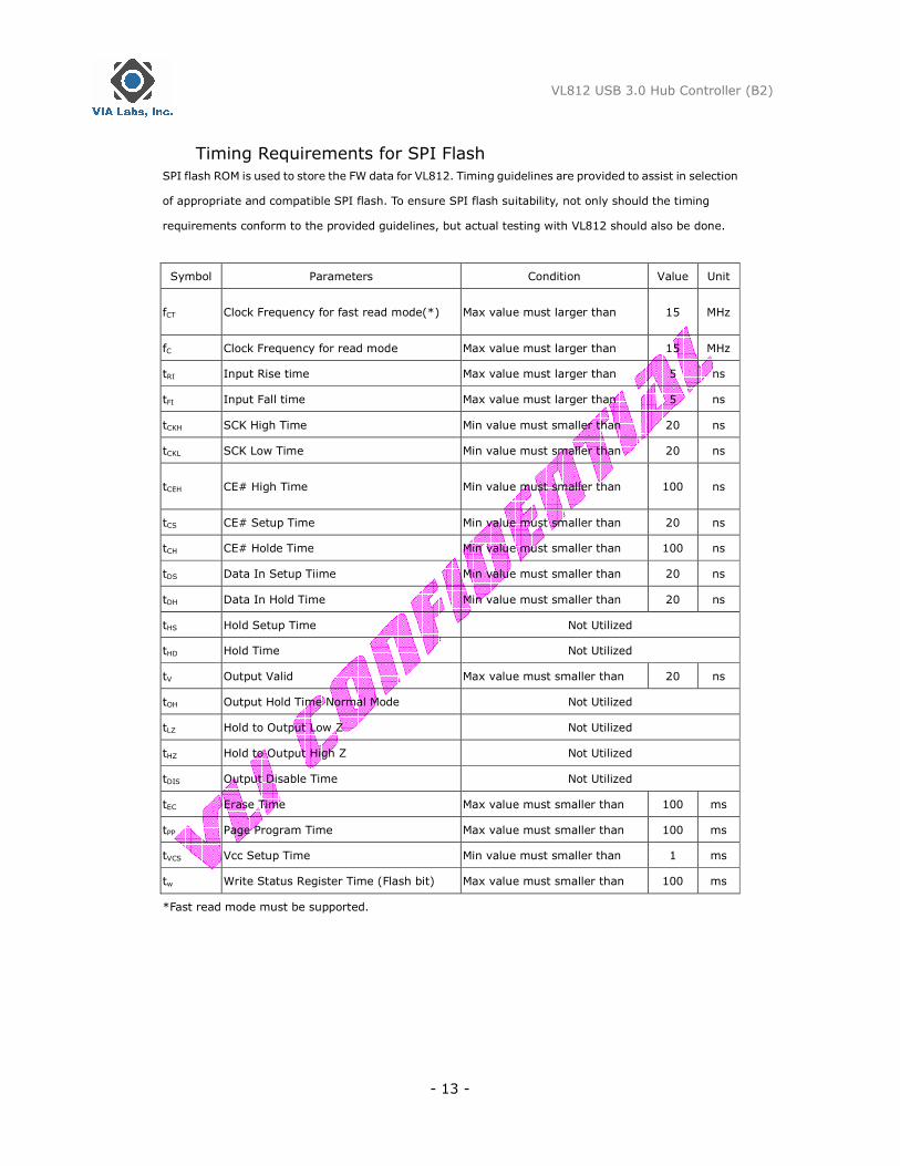
Timing Requirements for SPI Flash
SPI flash ROM is used to store the FW data for VL812. Timing guidelines are provided to assist in selection
of appropriate and compatible SPI flash. To ensure SPI flash suitability, not only should the timing
requirements conform to the provided guidelines, but actual testing with VL812 should also be done.
Symbol Parameters Condition Value Unit
fCT Clock Frequency for fast read mode(*) Max value must larger than 15 MHz
fC Clock Frequency for read mode Max value must larger than 15 MHz
tRI Input Rise time Max value must larger than 5 ns
tFI Input Fall time Max value must larger than 5 ns
tCKH SCK High Time Min value must smaller than 20 ns
tCKL SCK Low Time Min value must smaller than 20 ns
tCEH CE# High Time Min value must smaller than 100 ns
tCS CE# Setup Time Min value must smaller than 20 ns
tCH CE# Holde Time Min value must smaller than 100 ns
tDS Data In Setup Tiime Min value must smaller than 20 ns
tDH Data In Hold Time Min value must smaller than 20 ns
tHS Hold Setup Time Not Utilized
tHD Hold Time Not Utilized
tV Output Valid Max value must smaller than 20 ns
tOH Output Hold Time Normal Mode Not Utilized
tLZ Hold to Output Low Z Not Utilized
tHZ Hold to Output High Z Not Utilized
tDIS Output Disable Time Not Utilized
tEC Erase Time Max value must smaller than 100 ms
tPP Page Program Time Max value must smaller than 100 ms
tVCS Vcc Setup Time Min value must smaller than 1 ms
tw Write Status Register Time (Flash bit) Max value must smaller than 100 ms
*Fast read mode must be supported.
VL812 USB 3.0 Hub Controller (B2)
- 14 -
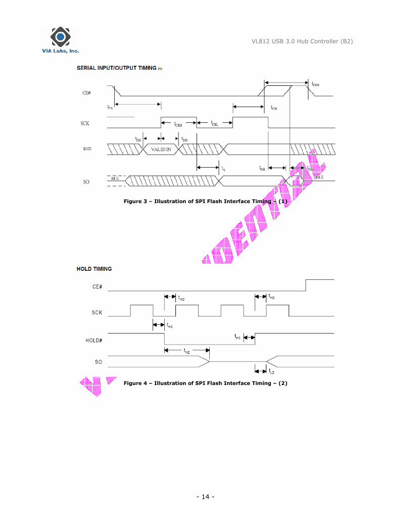
Figure 3 – Illustration of SPI Flash Interface Timing – (1)
Figure 4 – Illustration of SPI Flash Interface Timing – (2)
VL812 USB 3.0 Hub Controller (B2)
- 15 -
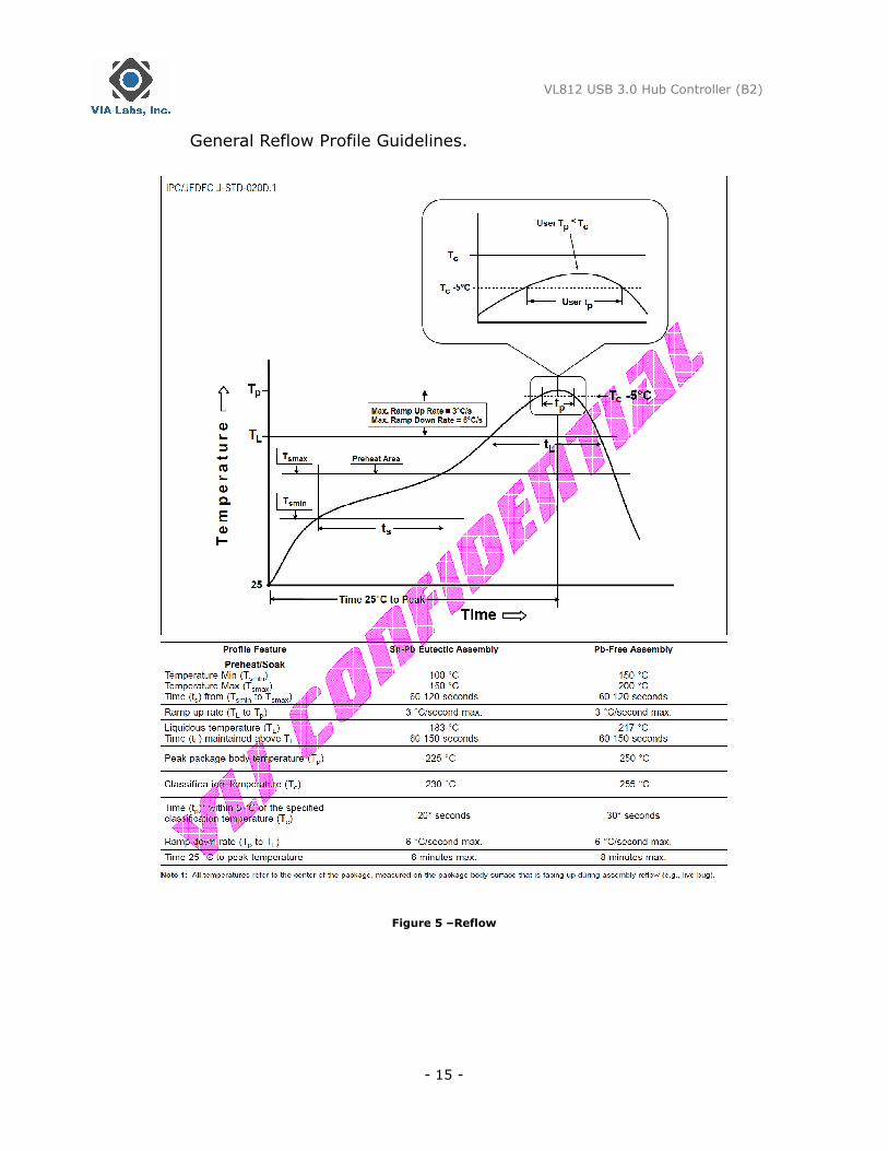
General Reflow Profile Guidelines.
Figure 5 –Reflow
VL812 USB 3.0 Hub Controller (B2)
- 16 -
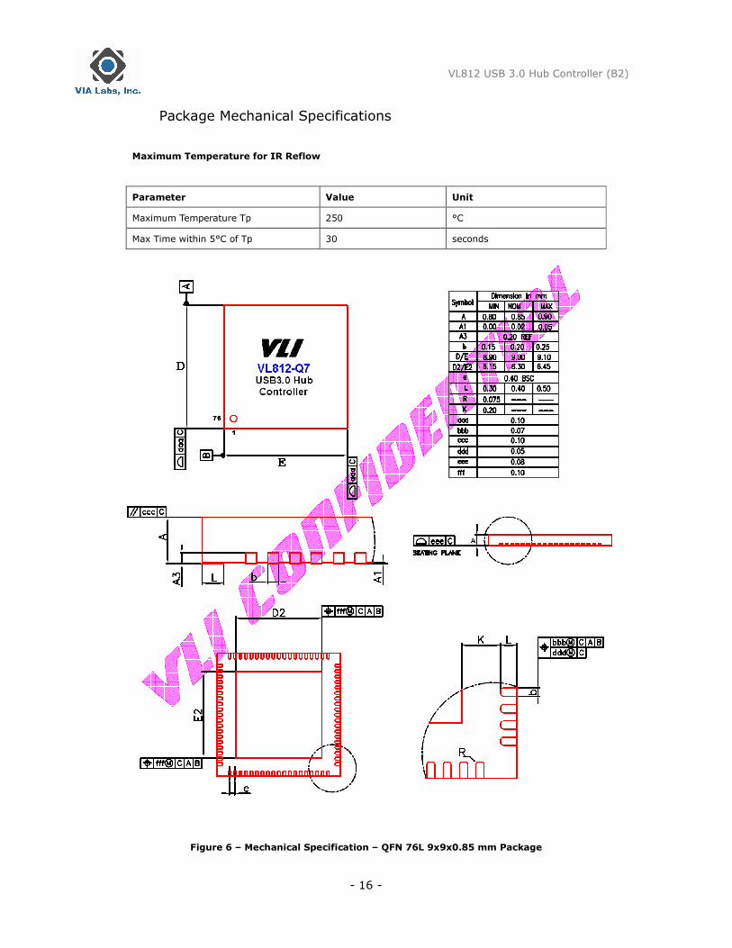
Package Mechanical Specifications
Maximum Temperature for IR Reflow
Parameter Value Unit
Maximum Temperature Tp 250 °C
Max Time within 5°C of Tp 30 seconds
Figure 6 – Mechanical Specification – QFN 76L 9x9x0.85 mm Package
VL812 USB 3.0 Hub Controller (B2)
- 17 -
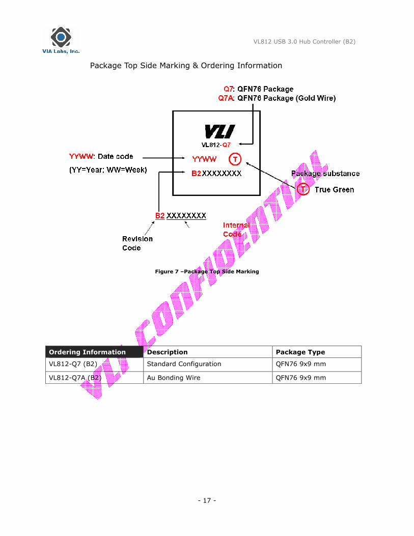
Package Top Side Marking & Ordering Information
Figure 7 –Package Top Side Marking
Ordering Information Description Package Type
VL812-Q7 (B2) Standard Configuration QFN76 9x9 mm
VL812-Q7A (B2) Au Bonding Wire QFN76 9x9 mm

VL812 USB 3.0 Hub Controller (B2)
- 18 -
VIA Labs, Inc.
www.via-labs.com
7F, 529-1, Zhongzheng Rd.,
Xindian District, New Taipei City 231 Taiwan
Tel: (886-2) 2218-1838
Fax: (886-2) 2218-8924
Email: [email protected]
Copyright © 2013 VIA Labs, Inc. All Rights Reserved. No part of this document may be reproduced, transmitted, transcribed, stored in a retrieval system, or translated into any language, in any form or by any means, electronic, mechanical, magnetic, optical, chemical, manual or otherwise without the prior written permission of VIA Labs, Inc. The material in this document is for information only and is subject to change without notice. VIA Labs, Inc. reserves the
right to make changes in the product design without reservation and without notice to its users. All trademarks are the properties of their respective owners. No license is granted, implied or otherwise, under any patent or patent rights of VIA Labs, Inc. VIA Labs, Inc. makes no warranties, implied or otherwise, in regard to this document and to the products described in this document. The information provided by this document is believed to be accurate and
reliable as of the publication date of this document. However, VIA Labs, Inc. assumes no responsibility for any errors in this document. Furthermore, VIA Labs, Inc. assumes no responsibility for the use or misuse of the information in this document and for any patent infringements that may arise from the use of this document. The information and product specifications within this document are subject to change at any time, without notice and without obligation to notify any person of such change.