dr.ntu.edu.sg · 85 the amount of overlap extrinsic parasitic capacitances will be larger when...
TRANSCRIPT

DESIGN OF A SCALABLE RF MODEL FOR DEEP
SUB-MICRON MOSFETS
TONG AH FATT
SCHOOL OF ELECTRICAL & ELECTRONIC ENGINEERING
A thesis submitted to the Nanyang Technological University
in fulfillment of the requirement for the degree of
Doctor of Philosophy
2010
ATTENTION: The Singapore Copyright Act applies to the use of this document. Nanyang Technological University Library

ii
ABSTRACT
In order to achieve first pass design success and optimized RF circuit
design, the process design kit (PDK) provided by the foundry must be equipped
with accurate and scalable RF models for circuit simulation and optimization
process. However, existing RF MOSFET models provided by most foundries are
usually in discrete sizes. This poses many design problems for the integrated
circuit (IC) designers because certain transistors’ geometry sizes are not available
in the PDK. Design optimization is not possible without scalable RFCMOS models
and the circuit performance cannot be optimized for a particular technology node
used for circuit fabrication. Furthermore, discrete RFCMOS models will limit the
design flexibility and increase the difficulty in designing RF circuit blocks to meet
more stringent design specifications as the operating frequency increases.
Currently in the industry, the RF MOSFET model that was developed is mainly in
BSIM3v3 and BSIM4 models. In BSIM3v3, the RF model is developed by macro
modeling approach whereby sub-circuit components are added to the core
transistor model. In BSIM4, the RF model for the parasitic components were
developed and included into the source code of the core model. Therefore,
theoretically, there is no need for the addition of the sub-circuit components as in
BSIM3v3 RF model. Although these two RF models are able to simulate the
transistor’s S-parameters, the sub-circuit components used are of discrete values.
Thus, scalable RF modeling is still not achieved. Therefore, there is a need to study
how to develop a scalable and physical RF MOSFET model.
Most of the RF models are developed based on the macro modeling
approach. Using this approach, sub-circuit components are added to the transistor’s
ATTENTION: The Singapore Copyright Act applies to the use of this document. Nanyang Technological University Library

iii
core model to model the RF parasitic components that will only appear at higher
frequency range. The extraction of these sub-circuit components are performed
with measured S-parameters but their extracted values can differ when different
extraction techniques are used. The various extraction techniques usually differ
from the DC biasing used for the RF extraction, different proposed equivalent
circuits and the extraction approach in obtaining these component values. By
studying the extracted parasitic component values with respect to the device’s
geometry, scalable geometry equations can be formulated to model the parasitic
components in the RF macro model. By simulating the RF model with scalable
geometry equations, the measured and simulated DC and S-parameters for a wide
range of device sizes can be compared and verified.
This thesis develops a systematic approach for the RF characterization,
modeling and simulation of deep sub-micron RF MOSFETs. In general, there are
four topics in this research work. Firstly, the geometry layout of the RF MOSFET
is studied and an experiment is designed to compare the change in the geometry
layout effect on the transistor’s figure of merits (FOMs). In the geometry variation,
the unit width of the transistor is varied but the total width is kept constant. Hence,
by comparing the various FOMs, the optimized unit width of the transistor can be
found for a particular technology. In this experiment, the FOM used for the
comparison are the unity short-circuit current gain frequency (fT), maximum
unilateral power gain frequency (fMAX), high frequency (HF) noise and flicker noise
performance.
Secondly, a new RF components extraction technique is presented. This
extraction technique utilizes both Z- and Y-parameters analysis on the proposed
small-signal equivalent circuit. The analytical equations are derived for all the RF
ATTENTION: The Singapore Copyright Act applies to the use of this document. Nanyang Technological University Library

iv
components and linear regression technique is used in the extraction. Excellent
agreement has been obtained between the simulated and measured results up to 20
GHz.
Thirdly, the formation of the parasitic components that exist in the RF
MOSFET structure at high frequency operations is presented. The parasitic
components are extracted from the transistor’s S-parameter measurement and its
geometry dependence is studied with respect to its layout structure. Physical
geometry equations are proposed to represent these parasitic components and by
implementing them into the RF model, a scalable RFCMOS model that is valid up
to 49.85 GHz is demonstrated. A new verification technique is proposed to verify
the quality of the developed scalable RFCMOS model.
Lastly, the HF noise modeling of RF MOSFET for a 90 nm technology
node is presented. A brief discussion on the noise measurement theory is presented
to illustrate the limitation of the noise measurement system. The extracted noise
sources were studied for their geometry and biasing dependences and by
implementing additional noise sources into the small-signal RFCMOS model,
accurate HF noise simulation for the transistor can be achieved. Verilog-A is used
for the coding of additional noise sources into the RFCMOS model and the added
noise source will compensate the under-estimation of the channel thermal noise
from the BSIM3v3 core model. Simulated noise circles and the measured noise
figures are plotted as other source impedances to show that all the noise parameters
are simulated accurately. The biasing and geometry dependences of the measured
and simulated noise parameters are presented to demonstrate the scalability of the
developed HF noise model.
ATTENTION: The Singapore Copyright Act applies to the use of this document. Nanyang Technological University Library

v
ACKNOWLEDGMENTS
I wish to thank my supervisor, Prof. Yeo Kiat Seng, for his constructive
advices and many fruitful discussions that we had during my research work.
Without his kind assistance, support and feedback, this research work will not be
completed. I also wish to thank Mr Lim Wei Meng for his support in taping out the
test-chip and performing the device measurement during this research and the
numerous discussions that we had has enhanced the quality of this research. I also
wish to thank Mr Sia Choon Beng from Cascade Microtech for his guidance in
device modeling and characterization when I was working in Advanced RFIC Pte.
Ltd.. I am also grateful to Mrs Jia Lin for her guidance in the device
characterization in the beginning years of my research study.
I wish to thank Takeshita, Abe and many other engineers from Sony Japan
for their valuable discussions in device modeling that helped to improve my
modeling technique.
I wish to thank the technical staffs in IC Design II Lab, Mr. Richard Tsoi,
Miss Guee Geok Lian and Mrs. Leong Min Lin, for the help they have given me
all these years.
Last but not least, I would like to thank my parents and my wife for their
support and encouragement in my research study.
ATTENTION: The Singapore Copyright Act applies to the use of this document. Nanyang Technological University Library

vi
TABLE OF CONTENTS
ABSTRACT .............................................................................................................ii
ACKNOWLEDGMENTS ....................................................................................... v
TABLE OF CONTENTS ........................................................................................ vi
LIST OF FIGURES ................................................................................................. x
LIST OF TABLES ................................................................................................ xvi
Chapter 1 INTRODUCTION ................................................................................ 1
1.1 Introduction................................................................................................... 1
1.2 Importance of RF Modeling and Existing Method ....................................... 4
1.3 Review of RF MOSFET Core Model ........................................................... 5
1.3.1 BSIM3v3 model ..................................................................................... 5
1.3.2 BSIM4 model ......................................................................................... 8
1.4 Objectives ..................................................................................................... 9
1.5 Major Contributions ................................................................................... 11
1.6 Thesis Organization .................................................................................... 12
Chapter 2 BASIC CONCEPTS FOR RF MODELING ...................................... 15
2.1 Introduction................................................................................................. 15
2.2 Z, Y, H and S-Parameters ........................................................................... 15
2.3 Smith Chart and Polar Plot ......................................................................... 20
2.3.1 Smith chart for Sxx ................................................................................ 20
2.3.2 Polar plot for Sxy ................................................................................... 21
2.4 Unity Short-Circuited Current Gain and Unilateral Power Gain Frequency
……... ................................................................................................................. 22
2.4.1 Unity short-circuited current gain frequency (fT) ................................. 22
2.4.2 Unilateral power gain frequency (fMAX) ................................................ 23
2.5 Types of Noise in Transistor....................................................................... 24
2.5.1 Thermal noise ....................................................................................... 24
2.5.2 Shot noise ............................................................................................. 24
2.5.3 Generation and recombination noise .................................................... 25
2.5.4 Flicker noise ......................................................................................... 25
2.5.5 Noise parameters and linear two-port noise theory .............................. 26
2.6 Summary ..................................................................................................... 28
Chapter 3 DEVICE CHARACTERIZATION .................................................... 30
ATTENTION: The Singapore Copyright Act applies to the use of this document. Nanyang Technological University Library
vii
3.1 Introduction................................................................................................. 30
3.2 DC Measurement ........................................................................................ 30
3.3 RF Measurement ......................................................................................... 31
3.3.1 S-parameter measurement system ........................................................ 32
3.3.2 Network analyzer calibration ............................................................... 34
3.3.3 Probe configuration and device layout ................................................. 36
3.3.4 De-embedding methods........................................................................ 38
3.3.4.1 OPEN de-embedding ..................................................................... 38
3.3.4.2 OPEN-SHORT de-embedding ....................................................... 39
3.3.5 De-embedding technique used and results ........................................... 41
3.4 Flicker Noise Measurement and Test Structure.......................................... 43
3.4.1 Flicker noise measurement system ....................................................... 44
3.4.2 Test structure ........................................................................................ 46
3.4.3 Measurement results ............................................................................. 46
3.5 High Frequency Noise Measurement and Test Structure ........................... 48
3.5.1 High frequency noise measurement system ......................................... 50
3.5.2 Test structure ........................................................................................ 52
3.5.3 System calibration and verification ...................................................... 52
3.5.4 High frequency noise de-embedding method ....................................... 55
3.6 Summary ..................................................................................................... 58
Chapter 4 CMOS RF MODELING .................................................................... 60
4.1 Introduction................................................................................................. 60
4.2 RF Parasitic in MOSFET ............................................................................ 60
4.2.1 Gate resistance modeling ..................................................................... 61
4.2.1.1 Poly-silicon gate electrode resistance (RG,poly) ............................... 61
4.2.1.2 Channel reflected gate resistance (RG,NQS) ..................................... 62
4.2.2 Source and drain resistances modeling ................................................ 62
4.2.3 Substrate resistances modeling ............................................................. 64
4.2.4 Parasitic capacitances modeling ........................................................... 65
4.3 BSIM3 – RF Model .................................................................................... 66
4.4 BSIM4 – RF Model .................................................................................... 69
4.4.1 Gate resistance model ........................................................................... 69
4.4.2 Substrate resistance Model ................................................................... 72
4.5 Summary ..................................................................................................... 73
ATTENTION: The Singapore Copyright Act applies to the use of this document. Nanyang Technological University Library

viii
Chapter 5 RFCMOS UNIT WIDTH OPTIMIZATION TECHNIQUE ............. 75
5.1 Introduction................................................................................................. 75
5.2 Design Experiment and Test Structure Layout ........................................... 77
5.3 Unit Width Optimization on fT and fMAX ..................................................... 78
5.3.1 fT definition and extraction ................................................................... 78
5.3.2 fMAX definition and extraction ............................................................... 80
5.3.3 Experimental results and discussion .................................................... 81
5.4 Unit Width Optimization on High Frequency Noise .................................. 87
5.4.1 HF noise definition and theory ............................................................. 87
5.4.2 Experimental results and discussion .................................................... 89
5.5 Proposal of New Figure of Merit for HF Noise .......................................... 91
5.6 Unit Width Optimization on Flicker Noise ................................................ 95
5.6.1 Experimental results and discussion .................................................... 96
5.7 Circuit Application Discussion ................................................................... 98
5.7.1 Transistor selection for LNA design .................................................... 98
5.7.2 Transistor selection for VCO design .................................................... 99
5.7.3 Transistor selection for Mixer design ................................................... 99
5.8 Summary ................................................................................................... 100
Chapter 6 SIMPLE AND ACCURATE EXTRACTION METHODOLOGY
FOR RF MOSFET VALID UP TO 20 GHZ ....................................................... 101
6.1 Introduction............................................................................................... 101
6.2 Measurement Setup .................................................................................. 103
6.3 Model ........................................................................................................ 103
6.3.1 Extraction of terminal resistances Rg, Rd and Rs ................................ 105
6.3.2 Extraction of intrinsic parasitic components ...................................... 106
6.4 Extraction and Simulation Results............................................................ 108
6.5 Summary ................................................................................................... 118
Chapter 7 SCALABLE RFCMOS TRANSISTOR MODELING AND ITS
VERIFICATION TECHNIQUE FOR RF CIRCUIT DESIGN .......................... 119
7.1 Introduction............................................................................................... 119
7.2 Scalable RF MOSFET Modeling.............................................................. 122
7.2.1 Gate resistance modeling ................................................................... 124
7.2.2 Source and drain resistance modeling ................................................ 127
7.2.3 Gate to substrate capacitance and resistance modeling ...................... 129
ATTENTION: The Singapore Copyright Act applies to the use of this document. Nanyang Technological University Library

ix
7.2.4 Gate to source and gate to drain capacitance modeling ..................... 133
7.2.5 Drain to source capacitance modeling ............................................... 136
7.2.6 Substrate resistances modeling ........................................................... 137
7.3 S-parameters Modeling Results ................................................................ 139
7.4 Proposed Scalable Model Verification Technique ................................... 146
7.5 RF Noise Modeling Results ...................................................................... 149
7.5.1 Noise source implementation ............................................................. 150
7.5.2 Measured and simulated noise parameters ......................................... 152
7.6 Summary ................................................................................................... 154
Chapter 8 A SCALABLE RFCMOS NOISE MODEL .................................... 156
8.1 Introduction............................................................................................... 156
8.2 HF Noise Measurement and Parasitic De-embedding .............................. 157
8.2.1 Test setup and parasitic de-embedding .............................................. 157
8.2.2 ATN NP5 measurement theory .......................................................... 160
8.3 Noise Source Extraction ........................................................................... 164
8.4 High Frequency Noise Modeling.............................................................. 170
8.4.1 Noise source implementation ............................................................. 171
8.4.2 Measured and simulated noise parameters ......................................... 173
8.5 Summary ................................................................................................... 185
Chapter 9 CONCLUSIONS AND RECOMMENDATIONS ........................... 187
9.1 Conclusions .............................................................................................. 187
9.2 Recommendations..................................................................................... 190
References ............................................................................................................ 192
Author’s Publications ........................................................................................... 207
Appendix A .......................................................................................................... 208
Verilog-A Codes for Current Control Current Source ..................................... 208
ATTENTION: The Singapore Copyright Act applies to the use of this document. Nanyang Technological University Library

x
LIST OF FIGURES
Fig. 1.1 Comparison of the input admittance for BSIM3v3 model with and
without gate resistance .............................................................................................. 7
Fig. 1.2 Comparison of the output admittance for BSIM3v3 model with and
without substrate resistance ...................................................................................... 8
Fig. 2.1 Z-parameter representation for two-port network ................................... 15
Fig. 2.2 Y-parameter representation for two-port network ................................... 16
Fig. 2.3 H-parameter representation for two-port network ................................... 17
Fig. 2.4 S-parameter representation for two-port network ................................... 19
Fig. 2.5 Relationship between Sxx and the complex impedance of a two-port ..... 20
Fig. 2.6 Polar plot for S12 and S21 ......................................................................... 21
Fig. 2.7 Noisy two-port network representation ................................................... 27
Fig. 3.1 S-parameter measurement system ........................................................... 32
Fig. 3.2 Known specific calibration terminations ................................................. 35
Fig. 3.3 RF GSG probes used in measurement ..................................................... 36
Fig. 3.4 RF transistor layout design ...................................................................... 37
Fig. 3.5 OPEN structure layout and its equivalent circuit .................................... 38
Fig. 3.6 SHORT structure layout and its equivalent circuit .................................. 39
Fig. 3.7 Comparison of the S-parameters before and after de-embedding of the
OPEN and SHORT structure .................................................................................. 43
Fig. 3.8 Flicker noise measurement system .......................................................... 44
Fig. 3.9 (a) DC and (b) RF transistor test structures ............................................. 46
Fig. 3.10 Measured (symbol) and simulated (solid line) DC results .................... 47
Fig. 3.11 Measured (red) and simulated (green) noise current spectral density ... 47
Fig. 3.12 ATN NP5B noise parameter and S-parameter device characterization
system ..................................................................................................................... 50
Fig. 3.13 Thru line S-parameter and noise verification ........................................ 55
Fig. 4.1 Distributed effects of the gate electrode and channel .............................. 61
ATTENTION: The Singapore Copyright Act applies to the use of this document. Nanyang Technological University Library

xi
Fig. 4.2 Source and drain parasitic resistances network ....................................... 63
Fig. 4.3 Different substrate configuration (a) 5-resistor, (b) 4-resistor, (c) 3-
resistor, (d) 2-resistor and (e) 1-resistor network .................................................... 64
Fig. 4.4 Parasitic capacitances in MOSFET ......................................................... 66
Fig. 4.5 RF BSIM3v3 macro model ...................................................................... 67
Fig. 4.6 BSIM4 RF model ..................................................................................... 69
Fig. 4.7 Geometrical details for the gate terminal in BSIM4 (a) NGCON =1 (b)
NGCON = 2............................................................................................................. 71
Fig. 4.8 Different gate resistance configuration with respect to RGATEMOD ... 72
Fig. 4.9 Five-substrate resistances network in BSIM4 ......................................... 73
Fig. 5.1 Designed test structure layout for a 15-finger thin gate NMOS transistor
................................................................................................................................. 78
Fig. 5.2 Measured H21 (dB) versus Frequency for an NMOS transistor with 10
fingers and Wf of 12 µm .......................................................................................... 79
Fig. 5.3 Measured GU (dB) versus Frequency for an NMOS transistor with 10
fingers and Wf of 12 µm .......................................................................................... 81
Fig. 5.4 Extracted fT and fMAX versus unit width for total width of (a) 48 µm, (b)
120 µm and (c) 240 µm........................................................................................... 83
Fig. 5.5 Extracted (a) maximum gm and Cg, (b) Rg and Cgd versus unit width for
total width of 48, 120 and 240 µm .......................................................................... 84
Fig. 5.6 Extracted NFmin (dB) versus Frequency with unit width of 4, 8, 12 and 24
µm for total width of (a) 48 µm, (b) 120 µm, (c) 240 µm ...................................... 91
Fig. 5.7 Measured and calculated Fmin·Rn (Ω) versus Frequency with unit width of
4, 8, 12 and 24 µm for total width of (a) 48 µm, (b) 120 µm, (c) 240 µm ............. 94
Fig. 5.8 Measured Flicker Noise Sid (A2/Hz) versus Frequency with unit width of
4, 8, 12 and 24 µm for total width of (a) 48 µm, (b) 120 µm and (c) 240 µm ........ 98
Fig. 6.1 New small-signal RF equivalent circuit ................................................ 103
Fig. 6.2 Simplified small-signal equivalent circuit at Vgs = 1.8 V and Vds = 0 V 105
Fig. 6.3 Simplified small-signal equivalent circuit at Vgs = Vds = 1.2 V (saturation
region) ................................................................................................................... 107
Fig. 6.4 Extraction of the transconductance gm and output conductance gds at Vgs =
Vds = 1.2 V ............................................................................................................. 109
ATTENTION: The Singapore Copyright Act applies to the use of this document. Nanyang Technological University Library
xii
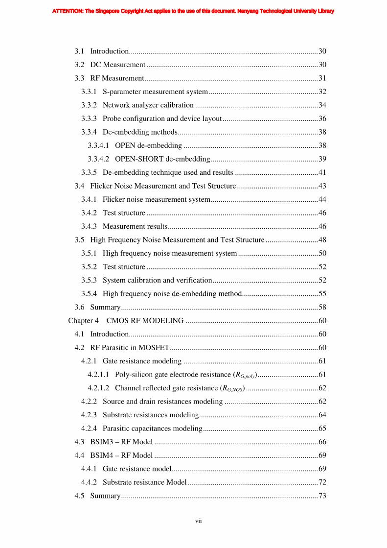
Fig. 6.5 Extraction of Rsubd at Vgs = Vds = 1.2 V from the plot of ω2/real (Ysub)
versus ω2 ............................................................................................................... 109
Fig. 6.6 Extraction of Rg, Rd and Rs at Vgs=1.8 V and Vds=0 V ........................... 110
Fig. 6.7 Frequency plot for Cgs, Cgd, Cdg, Cjd and Csd extracted at Vgs = Vds = 1.2 V
............................................................................................................................... 110
Fig. 6.8 Simulated and measured Y-parameters data for a 5-finger NMOS
transistor with length 0.18 µm and width 8 µm at Vgs = Vds = 1.2 V ..................... 114
Fig. 6.9 Simulated and measured results for 10*Log10(mag(H21)2) versus
Frequency in log scale for a 5-finger NMOS transistor with length 0.18 µm and
width 8 µm at Vgs = Vds =1.2 V .............................................................................. 115
Fig. 6.10 Gate bias dependence on the extracted (a) Capacitances and (b) Rsubd of
a 5-finger NMOS transistor with length 0.25 µm and width 8 µm biased at Vds =
1.2 V ...................................................................................................................... 116
Fig. 6.11 Drain bias dependence on the extracted (a) Capacitances and (b) Rsubd of
a 5-finger NMOS transistor with length 0.25 µm and width 8 µm biased at Vgs =
1.2 V ...................................................................................................................... 117
Fig. 7.1 RF equivalent sub-circuit model ............................................................ 122
Fig. 7.2 Simplified RF NMOS layout ................................................................. 123
Fig. 7.3 Simplified polysilicon gate structure and its distributed parasitic
resistances ............................................................................................................. 124
Fig. 7.4 Extracted and calculated Rgate versus (a) Nf and (b) Wf ......................... 127
Fig. 7.5 Source and drain metal structure ........................................................... 128
Fig. 7.6 Extracted and calculated (a) Rs and (b) Rd versus Nf ............................. 129
Fig. 7.7 Gate to substrate capacitance and resistance structure .......................... 130
Fig. 7.8 Extracted and calculated (a) Csubg and (b) Rsubg versus Nf ..................... 132
Fig. 7.9 Gate to source and gate to drain capacitance structure .......................... 134
Fig. 7.10 Extracted and calculated (a) Cgs_ext and (b) Cgd_ext versus Nf ............... 135
Fig. 7.11 Drain to source capacitance structure .................................................. 136
Fig. 7.12 Extracted and calculated Cds versus Nf ................................................ 136
Fig. 7.13 Substrate resistances network .............................................................. 137
Fig. 7.14 Extracted and calculated (a) Rsub1 and (b) Rsub2 and Rsub3 versus Nf .... 139
ATTENTION: The Singapore Copyright Act applies to the use of this document. Nanyang Technological University Library

xiii
Fig. 7.15 Measured and simulated results for NMOS transistor with Nf of 8, Wf of
1 µm and Lg of 70 nm ........................................................................................... 140
Fig. 7.16 Measured and simulated results for NMOS transistor with Nf of 24, Wf
of 1 µm and Lg of 70 nm ....................................................................................... 141
Fig. 7.17 Measured and simulated results for NMOS transistor with Nf of 64, Wf
of 1 µm and Lg of 70 nm ....................................................................................... 142
Fig. 7.18 Measured and simulated results for NMOS transistor with Nf of 24, Wf
of 2.5 µm and Lg of 70 nm .................................................................................... 143
Fig. 7.19 Measured and simulated results for NMOS transistor with Nf of 24, Wf
of 5 µm and Lg of 70 nm ....................................................................................... 144
Fig. 7.20 Model Accuracy for NMOSFETs with different Nf and Wf of 1, 2.5 and
5 µm at Vgs = 0.95 V and Vds = 0.8 V .................................................................... 147
Fig. 7.21 Model Continuity for Gm and Y21 for NMOSFETs with different Nf and
Wf of 1, 2.5 and 5 µm at Vgs = 0.95 V and Vds = 0.8 V .......................................... 148
Fig. 7.22 RF equivalent circuit model with added enhanced noise current 2
dei and
induced gate noise current 2
gi ............................................................................... 151
Fig. 7.23 Equivalent noise circuit (a) 2
dei and (b) 2
gi that generate additional noise
current [99] ............................................................................................................ 151
Fig. 7.24 Measured (symbol) and simulated (solid line) noise parameters versus
frequency for transistor with Nf of 32, Wf of 5 µm and Lg of 70 nm (Extracted Vds=
1.2 V @ Vgs= 0.55, 0.95 and 1.2 V) ...................................................................... 153
Fig. 7.25 Simulated noise circles and measured noise figures at different source
impedance states for transistor with Nf of 32, Wf of 5 µm and Lg of 70 nm
(Extracted at Vds= 1.2 V, Vgs= 0.55 V and frequency = 5 GHz) ........................... 154
Fig. 8.1 Noise parameters (a) NFmin and rn and (b) real(Γopt) and imag(Γopt) before
(solid line) and after (symbols) de-embedding of the pads and interconnects
parasitic for transistor with Nf of 32, Wf of 5 µm and Lg of 70 nm at Vgs = 0.95 V
and Vds = 1.2 V ...................................................................................................... 158
Fig. 8.2 Simplified RF NMOS layout ................................................................. 159
Fig. 8.3 Noise parameters (a) NFmin and rn and (b) real(Γopt) and imag(Γopt) before
(solid line) and after (symbols) de-embedding for transistor with Nf of 32, Wf of 1
µm and Lg of 70 nm at Vgs = 0.95 V and Vds = 1.2 V ............................................ 162
Fig. 8.4 DC characteristics (a) gm versus Vgs and (b) Ids versus Vds with measured
(symbols) and simulated (solid line) data for transistor with Nf of 32, Wf of 1 µm
and Lg of 70 nm ..................................................................................................... 164
ATTENTION: The Singapore Copyright Act applies to the use of this document. Nanyang Technological University Library
xiv
Fig. 8.5 Proposed RFCMOS model with extrinsic parasitic resistance noise,
intrinsic induced gate noise ( 2
gi ) and channel thermal noise ( 2
di ) ........................ 164
Fig. 8.6 Extracted noise sources (a) 2
di , (b) 2
gi and (c) *
dgii versus frequency for
transistors with Nf of 4, 16, 32 and 64 at fixed Wf of 5 µm and Lg of 70 nm
(Extracted at Vgs= 0.55 V and Vds= 1.2 V) ............................................................ 167
Fig. 8.7 Extracted noise sources (a) 2
di , (b) 2
gi and (c) *
dgii versus Wf for transistors
with Nf of 4, 16, 32 and 64 at fixed Lg of 70 nm (Extracted at Vgs= 0.55 V, Vds= 1.2
V and frequency = 5 GHz) .................................................................................... 168
Fig. 8.8 Extracted noise sources (a) 2
di , (b) 2
gi and (c) *
dgii versus Vgs for transistors
with Nf of 4, 16, 32 and 64 at fixed Wf of 5 µm and Lg of 70 nm (Extracted at Vds=
1.2 V and frequency = 5 GHz) .............................................................................. 169
Fig. 8.9 RF equivalent circuit model with added enhanced noise current 2
dei and
induced gate noise current 2
gi ............................................................................... 171
Fig. 8.10 Equivalent noise circuit (a) 2
dei and (b) 2
gi that generate additional noise
current [99] ............................................................................................................ 172
Fig. 8.11 Measured (symbol) and simulated (solid and dash line) noise parameters
versus frequency for transistor with Nf of 32, Wf of 5 µm and Lg of 70 nm
(Extracted at Vgs= 1.2 V and Vds= 1.2 V) .............................................................. 175
Fig. 8.12 Measured (symbol) and simulated (solid line) noise parameters versus
frequency for transistor with Nf of 32, Wf of 5 µm and Lg of 70 nm (Extracted Vds=
0.5 V @ Vgs= 0.55, 0.95 and 1.2 V) ...................................................................... 176
Fig. 8.13 Measured (symbol) and simulated (solid line) noise parameters versus
frequency for transistor with Nf of 32, Wf of 5 µm and Lg of 70 nm (Extracted Vds=
1.2 V @ Vgs= 0.55, 0.95 and 1.2 V) ...................................................................... 177
Fig. 8.14 Simulated noise circles and measured noise figures at different source
impedance states for transistor with Nf of 32, Wf of 5 µm and Lg of 70 nm (a) Vds=
1.2 V, Vgs= 0.55 V and (b) Vds= Vgs= 1.2 V (Extracted at frequency = 5 GHz)... 178
Fig. 8.15 Simulated noise circles and measured noise figures at different source
impedance states for transistor (a) Nf = 4, Wf = 1 µm, (b) Nf = 64, Wf = 1 µm, (c) Nf
= 4, Wf = 2.5 µm, (d) Nf = 64, Wf = 2.5 µm, (e) Nf = 4, Wf = 5 µm and (f) Nf = 64,
Wf = 5 µm at fixed Lg of 70 nm (Extracted at Vgs = Vds = 1.2 V and frequency = 5
GHz) ...................................................................................................................... 182
Fig. 8.16 Measured (symbol) and simulated (dash line) noise parameters versus
biasing for transistors with Wf (1, 2.5 and 5 µm) at fixed Nf of 32 (Extracted at Vds=
1.2 V and frequency = 5 GHz) .............................................................................. 184
ATTENTION: The Singapore Copyright Act applies to the use of this document. Nanyang Technological University Library

xv
Fig. 8.17 Measured (symbol) and simulated (dash line) noise parameters versus
transistors’ geometry with Nf (4, 16, 32 and 64) and Wf (1, 2.5 and 5 µm)
(Extracted at Vgs= Vds= 1.2 V and frequency = 5 GHz) ........................................ 185
ATTENTION: The Singapore Copyright Act applies to the use of this document. Nanyang Technological University Library

xvi
LIST OF TABLES
Table 1 RF characteristics of an NMOS with decreasing channel length [4] .......... 2
Table 5.1 Unit width optimization test structures fabricated in 0.18 µm CMOS
technology with a channel length of 0.18 µm ........................................................ 77
Table 6.1 Extracted and optimized parameter values for a 5-finger NMOS
transistor with L = 0.18 µm and W = 8 µm at Vgs = Vds = 1.2 V .......................... 112
ATTENTION: The Singapore Copyright Act applies to the use of this document. Nanyang Technological University Library

1
Chapter 1
INTRODUCTION
1.1 Introduction
The radio frequency (RF) wireless technology has changed the way people
communicate and transfer of information. The various technologies like the 3G
cellular phones, global positioning system (GPS) and Bluetooth have advanced
greatly and allow people to be connected at almost anywhere anytime in the world.
In the past, wireless products like the cellular phone were very bulky and their
operating power consumption was high. In order for cellular phone to be mobile,
we need to reduce the size of the product and also improve its power efficiency so
that the product can operate for a longer period of time. To achieve the size
reduction and power efficiency, RF integrated circuit (IC) technology was
developed.
Basically, RF IC is made up of high-speed transistors and passive
components like the resistors, capacitors and inductors. The main parameters
determining the performance of a RF IC are the operating frequency range, gain,
noise, linearity and the power efficiency. Presently, the majority of the RF IC’s are
typically implemented using GaAs or silicon bipolar technology [1], [2]. This is
because GaAs and bipolar transistors have high unity cut-off frequency. As for the
Complementary-Metal-Oxide-Semiconductor (CMOS) technology, its transistors
are inferior as compared to GaAs and bipolar counterparts in terms of the
microwave properties. But as the channel length of the Metal-oxide-
Semiconductor Field Effect Transistor (MOSFET) scales down, both the unity
ATTENTION: The Singapore Copyright Act applies to the use of this document. Nanyang Technological University Library

2
current gain frequency (fT) and unilateral power gain frequency (fMAX) will increase
while the minimum noise figure (NFmin) will reduce. From Table 1, the fT and fMAX
for a 0.18 µm technology is about 50 GHz and the NFmin is about 0.35 dB at 2 GHz
operation frequency. This shows that CMOS technology is becoming a viable
technology choice for RF integrated components for the wireless communication
market [3].
Table 1 RF characteristics of an NMOS with decreasing channel length [4]
Gate Length, L (nm) 250 180 140 120 100
fT (GHz) 33 49 70 84 112
fMAX (GHz) 41 47 51 52 60
NFmin (dB) @ 2 GHz 0.5 0.35 0.23 0.2 0.15
Apart from the above improvements, CMOS technology also offers high
integration density, low cost and the ability to integrate digital, low frequency
analog and RF circuits into a single chip. Furthermore, the low power consumption
of MOSFET makes the technology suitable for portable devices.
The two main differences of the RF MOSFET and the conventional high-
speed transistors are the substrate material and the device structure [5]. For
MOSFET, it is fabricated on a silicon substrate, which is a semi-conducting
material unlike the GaAs, which is a semi-insulating material. The typical
resistivity range for silicon is 0.01 to 10 Ω-cm while the GaAs is about 108 Ω-cm
[5]. The low resistivity of the silicon substrate produces more parasitic in the
MOSFET’s layout and these parasitic can affect the performance of the RF device.
At high operating frequency, the substrate coupling effect for the RF MOSFET
will become dominant when the impedance of the source and drain junction
ATTENTION: The Singapore Copyright Act applies to the use of this document. Nanyang Technological University Library
3
capacitance starts to drop [6-10]. As for the bonding pads that connect the RF
transistors, the parasitic capacitance between the signal pads and ground pads will
increase due to the low resistivity of the silicon substrate [11]. Therefore, the de-
embedding of the parasitic capacitance must be done in order to obtain the intrinsic
RF MOSFET performance. As for the passive components such as the inductor,
the energy dissipation through the silicon substrate significantly reduces the
performance of the on-chip inductor [12-14]. When the operating frequency
increases, the electric field from the interconnect structure will appear in the lossy
silicon substrate, the signal will propagate in dielectric quasi-TEM mode. The
signal propagation will be very complex and the modeling of interconnects will be
difficult [15-17]. As the CMOS technology allows the integration of the digital,
low frequency analog and RF circuits, the signal and noise coupling between these
blocks will be an issue as the substrate is lossy [18-21].
The second difference between the MOSFET and the conventional RF
transistor is the layout structure of the device. The conventional RF transistor like
the bipolar transistors consists of three terminals, the base, the collector and the
emitter. Therefore, it can be treated as a two-port network. As the RF measurement
technique for the two-port network is well established, the S-parameters can be
collected and analysed easily. The MOSFET consists of four terminals: gate, drain,
source and body. Normally, the source and the body terminals are connected to
each other, so that it becomes like a three-terminal device. But as the operating
frequency increases, the AC substrate current will increase and flows through the
distributed RC network in the substrate. This will cause the potential of the
intrinsic substrate node to be different from the source and the extrinsic body
terminal. Therefore to model a four-terminal MOSFET, additional DC
ATTENTION: The Singapore Copyright Act applies to the use of this document. Nanyang Technological University Library
4
measurements must be made to characterize the biasing effect on the body
structure. Since the biasing effect of the body structure can be characterized in the
DC measurement, the source and the body terminals can be shorted together and
measured as a two-port network during the RF measurement so as to extract its
characteristic and the RF parasitic of the device layout.
1.2 Importance of RF Modeling and Existing Method
Presently, circuit simulation is the only way for RF circuit designer to
predict the performance of the designed RF circuit before committing to silicon
fabrication. The accuracy of circuit simulation is mainly dependent on the
availability of accurate device models and interconnect parasitic. Hence, the
number of design cycles and the time to market of the product can be reduced if
accurate device models are provided.
Most of the MOSFET models have been developed for digital and low
frequency analog circuit design [22-23], which focus on the DC characteristics and
the low frequency performance up to several tens of MHz frequency range. But as
the operating frequency increases, the extrinsic parasitic of the transistor will
become more dominant and cannot be ignored anymore. Therefore, the
commercially available digital and low frequency models can no longer be used
for high frequency (HF) simulation. In order to achieve accurate HF simulation,
the RF model must include both the intrinsic and extrinsic parasitic components.
The initial method for RF modeling is by using the table lookup method.
This method has its advantages and disadvantages. In this method, the device
characteristics are measured and then stored or translated into mathematical
functions, which can then reproduce the data with minimum error. Therefore, there
ATTENTION: The Singapore Copyright Act applies to the use of this document. Nanyang Technological University Library

5
is no need for parameter extraction. Furthermore, this method is technology
independent. The procedure to develop such a table can be reuse for any
technology whereas for physical models, modeling equations and parameter
extraction method may have to change for different technologies.
As for the disadvantages, this method requires to measure many different
transistor sizes so as to collect all their device characteristics and organise them in
tabular form. During the circuit design, if the transistor size that the designer
requires for the simulation is not in the lookup table, the lookup table must be
updated by performing HF measurement on the required transistor size. If the
required transistor is not fabricated then there is no way to predict the required
transistor size performance. Therefore, this method requires a lot of measurement
time to develop and it is unable to predict the HF performance of the device if the
device size is not in the table. Furthermore, this method cannot be use to predict
the device characteristics for the next generation technology. Hence, due to the
above problems, macro modeling approach is adopted for the modeling of RF
MOSFET. In the macro modeling approach, parasitic components that simulate the
RF parasitic at higher frequency are added to the core transistor model. By adding
the parasitic components, the generated RF MOSFET model is more complete and
it can simulate the RF characteristics more accurately.
1.3 Review of RF MOSFET Core Model
1.3.1 BSIM3v3 model
BSIM3v3 is a DC scalable MOSFET model. It is considered as a physical
model because most of its parameters have strong correlation to the process and
device structure design. But there are also some parameters that have weak
ATTENTION: The Singapore Copyright Act applies to the use of this document. Nanyang Technological University Library

6
physical meaning and are only introduced for the model fitting purposes. BSIM3v3
has been widely used by the industry and is initially developed for analog and
digital circuit simulation. But for the RF simulation, it lacks of some important
models that are required to predict the RF parasitic and therefore, sub-circuit
components are added to the core model to simulate the RF parasitic effects [9]
using the macro modeling approach.
In the core model, the gate resistance Rg is not included and hence it is
unable to accurately predict the input admittance as shown in the Figure 1.1. It is
important for the RF model to be able to predict the measured input admittance
due to the power matching requirement. As Rg also contributes to the total thermal
noise of the MOSFET, it will directly affect the simulated noise figure of the
transistor. Furthermore, the unilateral power gain frequency fMAX will be shown in
chapter 2, in equation (2-29) to be dependent on Rg. Hence based on the above
simulation issues, it is crucial to study the effect of Rg so that accurate model can
be developed for it.
At DC and low frequency region, Rg is purely the gate electrode resistance.
But as the frequency increases, the gate electrode must be treated as a distributed
transmission line [24] so as to model Rg accurately.
N
wLj
N
Lw
wCj
NZ
spoly
p
in
33
/ ωρ
ω++= , Single contacted gate (1-1)
N
wLj
N
Lw
wCj
NZ
spoly
p
in
1212
/ ωρ
ω++= , Double contacted gate (1-2)
By treating the gate terminal as a distributed transmission line, the gate
impedance can be derived as in (1-1) and (1-2). The variable N is defined as the
number of finger, Cp is the gate capacitance, ρpoly is the gate resistivity, L and w is
the length and width of a single finger, and Ls is the series inductance in the gate
ATTENTION: The Singapore Copyright Act applies to the use of this document. Nanyang Technological University Library

7
terminal. A detailed derivation for (1-1) and (1-2) can be obtained in [24]. Based
on the two equations, it is obvious that the effect of the distributed gate resistance
becomes important especially for wide transistors and by using multi-finger layout,
this distributed effect can be minimised. Another physical effect is the distributed
or non-quasi-static (NQS) effect in the channel [9]. This will be discussed in
greater detail in the following chapters.
Fig. 1.1 Comparison of the input admittance for BSIM3v3 model with and
without gate resistance
Since the substrate coupling effect is not modelled in BSIM3v3, the output
admittance of the transistor is unable to be modelled accurately as the output
admittance is closely related to the substrate coupling at the drain and source
junctions. Figure 1.2 shows the effect of the substrate coupling in predicting of the
0.000
0.001
0.002
0.003
0.004
0.005
0.006
0.007
0.008
0 5 10 15 20 25Frequency (GHz)
Real(
Y1
1)
an
d Im
ag
(Y1
1)
(S)
Imag (Y11)
Real (Y11)
Wf = 8µµµµm
L = 0.18µµµµm Nf = 5 Vds = Vgs = 1.2V
Real (Y11_meas) Real (Y11_with_Rg) Real (Y11_without_Rg)
ATTENTION: The Singapore Copyright Act applies to the use of this document. Nanyang Technological University Library

8
output admittance. Therefore, it is clear that the substrate coupling network must
be added into the RF model to accurately predict the output admittance.
0.000
0.001
0.002
0.003
0.004
0.005
0.006
0.007
0.008
0.009
0 5 10 15 20 25
Frequency (GHz)
Re
al
(Y22)
an
d I
ma
g (
Y22)
(S)
Real (Y22)
Imag (Y22)
Fig. 1.2 Comparison of the output admittance for BSIM3v3 model with and
without substrate resistance
The common approach for RF modeling for BSIM3v3 is by adding sub-
circuit components to model the Rg and Rsub resistances [9] and several others RF
parasitic effect. Several other models with different sub-circuit components are
reported in [25-30].
1.3.2 BSIM4 model
In BSIM4, the Rg effect is now included into its core model. Its resistance
is being separated into the gate electrode resistance and the channel-reflected
resistance. As the operating frequency increases, the gate electrode is being treated
as a distributed resistance so that it can be modelled more accurately. The gate
Wf = 8µµµµm
L = 0.18µµµµm Nf = 5 Vds = Vgs = 1.2V
Imag (Y22_simu_with_Rsub)
Imag (Y22_meas)
Imag (Y22_simu_without_Rsub)
Real (Y22_simu_with_Rsub)
Real (Y22_meas)
Real (Y22_simu_without_Rsub)
ATTENTION: The Singapore Copyright Act applies to the use of this document. Nanyang Technological University Library

9
electrode resistance is derived as in (1-1) and (1-2). The channel-reflected
resistance is not a physical resistance. It is the resistance as “seen” by the gate
signal and is a function of biasing [31]. This channel-reflected gate resistance is
one of the various approaches to account for the NQS effect [31]. Quasi-Static
(QS) is defined as the ability for the charges in the channel to respond immediately
to the biasing and most of the commercially available models are QS models.
When the RF MOSFET is operated at high frequency, the response speed of the
device to the input biasing may not be fast enough and the device will show some
signal delay, this is defined as NQS effect. In BSIM4, different configuration of
the Rg model can be selected with the parameter RGATEMOD.
In BSIM3v3, there is no internal substrate resistance and hence the model
is unable to fit the output admittance of the RF MOSFET. In BSIM4, the substrate
resistances are now being modelled by a five resistors network. The substrate
network can be selected by the parameter RBODYMOD. Note that this substrate
network is not scalable, as they have no geometry dependence parameter in the
model [32].
1.4 Objectives
In RF modeling, although the sub-circuit model approach for BSIM3v3
have been widely used and found to be sufficient, the associated parasitic
extraction technique must still be improved so as to achieve a more robust
extraction method.
In BSIM4, the inclusion of the gate and substrate resistances model has
made BSIM4 another alternative for RF modeling. But as the proposed substrate
network in BSIM4 is not scalable, it is unable to predict the RF characteristics for
ATTENTION: The Singapore Copyright Act applies to the use of this document. Nanyang Technological University Library

10
different geometry sizes [32]. Similarly, for BSIM3v3 model, the sub-circuit
components that are used to model the substrate resistances are also not scalable
with geometry. Therefore, there is a need to improve the model so as to achieve RF
scalability.
The goal of this thesis is to design a scalable RF model for deep sub-
micron MOSFETs. Basically, four main objectives are required to fulfill in this
research. Firstly, the layout of the RF MOSFET is studied and the relationship
between its geometry layout and its corresponding HF parasitic effect is compared
and analyzed. This study will enhance our device layout knowledge so that an
optimized geometry design can be found for a particular RF circuit design.
Secondly, there are many different RF parameter extraction techniques proposed
and published in this research and each technique produces different extracted
values for the RF components. Therefore, there is a need to study the various
published extraction techniques in greater details so as to understand their pro and
cons and the assumptions in their proposed techniques. With the knowledge of the
various extraction techniques, a new and accurate method is investigated for the
extraction of the RF sub-circuit components.
Thirdly, most of the RF models provided by the foundry are for discrete sizes.
So, when circuit designers tune or optimize their circuits, they will be limited by
the number of device sizes available from the process design kit (PDK). Therefore,
this research will study the geometry dependence of the extracted parasitic
components and implementing them into the RF model so that a scalable
RFCMOS model can be demonstrated.
Finally, in order to develop a truly scalable RFCMOS model, it should be
scalable in terms of its DC, S-parameters, flicker noise and HF noise
ATTENTION: The Singapore Copyright Act applies to the use of this document. Nanyang Technological University Library

11
characteristics. In the RFCMOS noise modeling, the flicker noise model provided
in BSIM is well established and is already scalable with geometry and biasing. But
the HF noise model provided in the BSIM models underestimates the device noise
performance. Hence, this research aims to improve the HF noise modeling with
respect to the model’s accuracy and scalability in terms of the device’s geometry
and biasing.
1.5 Major Contributions
In this thesis, four major contributions are accomplished and they are listed as
follows.
1. By studying the measured fT, fMAX, flicker noise and HF noise characteristics of
the RFCMOS transistors for different unit width for a given fixed total width,
the geometry dependence of the parasitic components is studied and optimized
for a particular RF circuit design [33].
2. Proposed an accurate and simple parameter extraction technique for deep sub-
micron MOSFETs. The as-developed RF model demonstrates excellent model
accuracy up to 20 GHz [34].
3. By studying the geometry dependence of the parasitic components, a scalable
RFCMOS model is successfully implemented that is valid up to 49.85 GHz. In
addition, a new verification technique is proposed to verify the quality of the
as-developed scalable RFCMOS model. The verification time of the scalable
model is shortened and the coded scalable model equations are checked for its
reliability to use.
4. High frequency (HF) noise modeling of RF MOSFET for a 90 nm technology
node is demonstrated. The pads and interconnects parasitic are de-embedded to
ATTENTION: The Singapore Copyright Act applies to the use of this document. Nanyang Technological University Library

12
obtain the true device noise performance and noise sources are extracted from
the proposed noise equivalent circuit. By implementing the geometry and
biasing dependence of the noise sources into the RF model, an accurate and
scalable HF noise model is generated [36].
1.6 Thesis Organization
This thesis consists of nine chapters. In chapter 1, the importance of RF
modeling is discussed and a review of the core RF MOSFET model is presented.
Various objectives and major contributions in the course of this research, follow by
the organization of this thesis are also given.
Chapter 2 presents the basic concepts of RF modeling which includes the
linear two-port network theory. The knowledge of the various two-port networks
are essential for de-embedding of pads and interconnects parasitic, the extraction
of the RF sub-circuit components and the fT and fMAX parameters calculation. The
different type of noise that exists in MOS devices is presented and the linear two-
port noise theory and the noise parameters are discussed in this chapter.
Chapter 3 shows the various measurement results performed during the
course of this research. The DC characteristics, S-parameters, flicker noise and the
HF noise parameters are measured during the characterization of RF MOSFET. In
the section of RF measurement, the measurement system and the device layout are
presented and system calibration is performed to remove the errors and parasitic
from the measurement setup to the probe pins plane. By performing Z and Y
parameters calculations, the de-embedding of the pads and interconnects parasitic
can be done so that the true device performance can be obtained. The measurement
system of the flicker noise and HF noise is presented together with its
ATTENTION: The Singapore Copyright Act applies to the use of this document. Nanyang Technological University Library

13
corresponding calibration steps. The noise contribution from the parasitic can be
removed from the measured results to obtain the true noise behaviour.
In order to perform RF modeling, it is essential to know about all the RF
parasitic that will appear at RF frequency range. Hence in chapter 4, all the RF
parasitic that exist in the RF MOSFET will be discussed. The RF model of
BSIM3v3 and BSIM4 will also be presented.
After the RF parasitic are discussed, it is important to understand how these
RF parasitic changes with geometry and their effects on the FOMs for RF
MOSFET. By understanding the relationship between the device geometry and the
RF parasitic, the layout of the device can be optimized such that optimum device
performance can be achieved. In chapter 5, FOMs such as fT, fMAX, flicker noise
and HF noise parameters are optimized with geometry. A new FOM is proposed
for the study of HF noise performance of transistor. A brief discussion on the
transistor geometry requirement for RF circuit design such as low noise amplifier
(LNA), voltage controlled oscillator (VCO) and mixer is given.
In chapter 6, a simple and accurate extraction methodology for RF
MOSFET is proposed and the extraction is shown to be reliable up to 20 GHz.
Based on literature review on the conventional and current extraction techniques, a
new technique is proposed for the RF parasitic extraction. By implementing the
extracted values for a 5 finger NMOS transistor, it is shown that the generated
model is valid up to 20 GHz.
In chapter 7, a scalable RFCMOS transistor modeling and its model
verification technique is demonstrated. The various RF parasitic components used
in the proposed scalable RF model are presented in detail with their formulated
geometry equations. The transistor’s finger and unit width scalability are
ATTENTION: The Singapore Copyright Act applies to the use of this document. Nanyang Technological University Library

14
demonstrated for the DC, S-parameters and fT plots. A new model verification
technique is proposed for scalable RF model whereby the model’s accuracy and
continuity are checked and verified.
Presently, RFCMOS noise modeling is mainly used for discrete transistor
size only. Therefore, in order to enhance the PDK’s features and help circuit
designers to optimize the noise critical circuit blocks, scalable RFCMOS noise
modeling must be developed. In chapter 8, by using the reported techniques,
measured noise parameters are de-embedded from the pads and interconnects
parasitic. And with the proposed noise equivalent circuit, its noise sources can be
extracted from the de-embedded noise parameters. By implementing the noise
sources using Verilog-A into the RF model, the generated scalable RF noise model
can be simulated accurately for a wide range of geometry, biasing and frequency.
Finally in chapter 9, the thesis will conclude all the research work done and
a discussion will be done on the possible future work in this research area.
ATTENTION: The Singapore Copyright Act applies to the use of this document. Nanyang Technological University Library

15
Chapter 2
BASIC CONCEPTS FOR RF MODELING
2.1 Introduction
The linear two-port network theory has been widely studied and used by
many engineers to characterize the electrical behavior of devices. Basically, a
RFCMOS transistor is a four terminal device and it consists of the gate, drain,
source and body terminal. As the body terminal is not connected to ground, its
potential will affect the charges in the channel and caused the threshold voltage of
the transistor to vary. Therefore, in order to eliminate the body biasing effects on
the substrate, the body terminal is usually tied to the source terminal and the
transistor becomes a three terminal device. By grounding the source and body
terminal, the RFCMOS transistor can be treated as a two-port device so that the
two-port network theory can be used to describe the transistor electrical behavior.
The different types of two-port network are presented and used in this thesis.
2.2 Z, Y, H and S-Parameters
Fig. 2.1 Z-parameter representation for two-port network
_ _
+
Z11 Z22 I1
(Port 1) V1 Z12I2
I2
(Port 2) V2 Z21I1
+
ATTENTION: The Singapore Copyright Act applies to the use of this document. Nanyang Technological University Library

16
Fig. 2.1 shows the two-port network for the Z-parameters and their
representations are derived in the following equations.
2121111 IZIZV += (2-1)
2221212 IZIZV += (2-2)
Based on (2-1) and (2-2), all the Z-parameters can be extracted by opening
of port 1 and 2 in Fig. 2.1 and their corresponding equations are derived in (2-3) to
(2-6).
021
111
==
II
VZ (2-3)
012
112
==
II
VZ (2-4)
021
221
==
II
VZ (2-5)
012
222
==
II
VZ (2-6)
Fig. 2.2 Y-parameter representation for two-port network
Fig. 2.2 shows the two-port network for the Y-parameters and their
representations are derived in the following equations.
2121111 VYVYI += (2-7)
2221212 VYVYI += (2-8)
Y22
I1
(Port 1) V1 Y12V2 Y11
I2
(Port 2) V2 Y21V1
ATTENTION: The Singapore Copyright Act applies to the use of this document. Nanyang Technological University Library

17
Based on (2-7) and (2-8), all the Y-parameters can be extracted by shorting
of port 1 and 2 in Fig. 2.2 and their corresponding equations are derived in (2-9) to
(2-12).
021
111
==
VV
IY (2-9)
012
112
==
VV
IY (2-10)
021
221
==
VV
IY (2-11)
012
222
==
VV
IY (2-12)
Fig. 2.3 H-parameter representation for two-port network
Fig. 2.3 shows the two-port network for the H-parameters and their
representations are derived in the following equations.
2121111 VHIHV += (2-13)
2221212 VHIHI += (2-14)
Based on (2-13) and (2-14), all the H-parameters can be extracted by
opening of port 1 and shorting of port 2 in Fig. 2.3 and their corresponding
equations are derived in (2-15) to (2-18).
_
+
H11
H22
I1 (Port 1) V1 H12V2
I2
(Port 2) V2 H21I1
ATTENTION: The Singapore Copyright Act applies to the use of this document. Nanyang Technological University Library
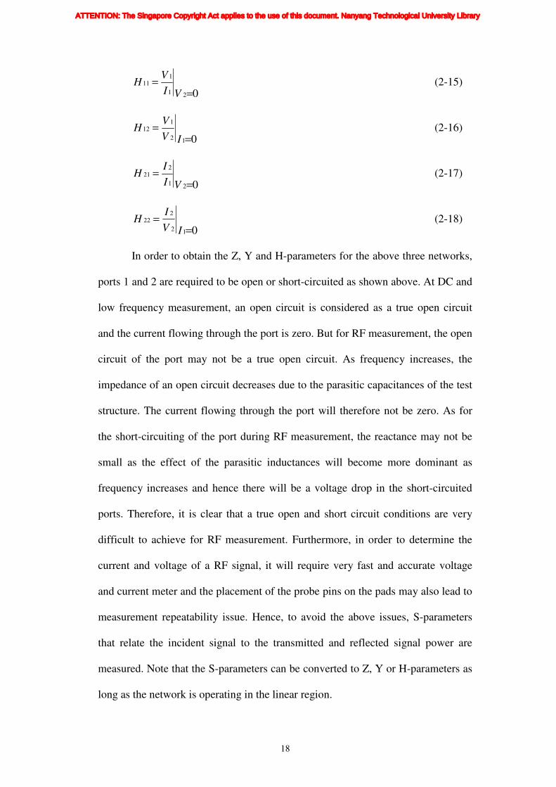
18
021
111
==
VI
VH (2-15)
012
112
==
IV
VH (2-16)
021
221
==
VI
IH (2-17)
012
222
==
IV
IH (2-18)
In order to obtain the Z, Y and H-parameters for the above three networks,
ports 1 and 2 are required to be open or short-circuited as shown above. At DC and
low frequency measurement, an open circuit is considered as a true open circuit
and the current flowing through the port is zero. But for RF measurement, the open
circuit of the port may not be a true open circuit. As frequency increases, the
impedance of an open circuit decreases due to the parasitic capacitances of the test
structure. The current flowing through the port will therefore not be zero. As for
the short-circuiting of the port during RF measurement, the reactance may not be
small as the effect of the parasitic inductances will become more dominant as
frequency increases and hence there will be a voltage drop in the short-circuited
ports. Therefore, it is clear that a true open and short circuit conditions are very
difficult to achieve for RF measurement. Furthermore, in order to determine the
current and voltage of a RF signal, it will require very fast and accurate voltage
and current meter and the placement of the probe pins on the pads may also lead to
measurement repeatability issue. Hence, to avoid the above issues, S-parameters
that relate the incident signal to the transmitted and reflected signal power are
measured. Note that the S-parameters can be converted to Z, Y or H-parameters as
long as the network is operating in the linear region.
ATTENTION: The Singapore Copyright Act applies to the use of this document. Nanyang Technological University Library
19
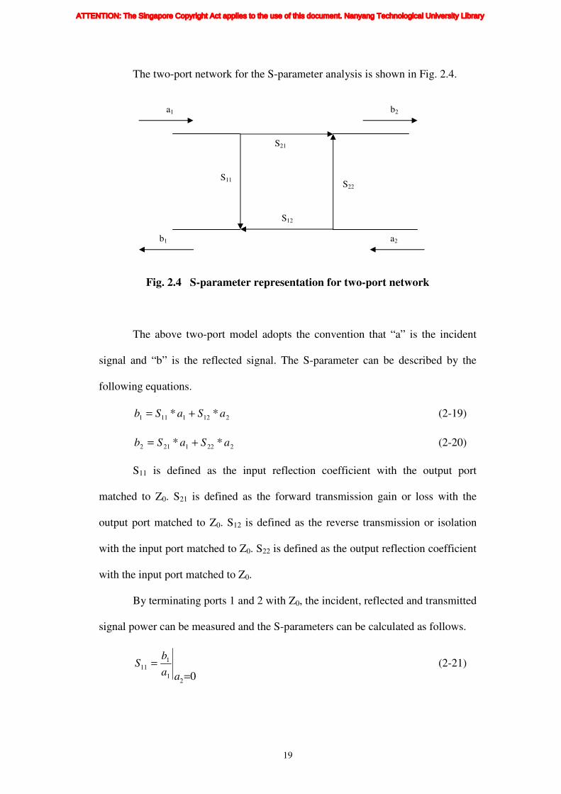
The two-port network for the S-parameter analysis is shown in Fig. 2.4.
Fig. 2.4 S-parameter representation for two-port network
The above two-port model adopts the convention that “a” is the incident
signal and “b” is the reflected signal. The S-parameter can be described by the
following equations.
2121111 ** aSaSb += (2-19)
2221212 ** aSaSb += (2-20)
S11 is defined as the input reflection coefficient with the output port
matched to Z0. S21 is defined as the forward transmission gain or loss with the
output port matched to Z0. S12 is defined as the reverse transmission or isolation
with the input port matched to Z0. S22 is defined as the output reflection coefficient
with the input port matched to Z0.
By terminating ports 1 and 2 with Z0, the incident, reflected and transmitted
signal power can be measured and the S-parameters can be calculated as follows.
02
1
111
==
aa
bS (2-21)
a2 b1
S21
S12
S11 S22
a1 b2
ATTENTION: The Singapore Copyright Act applies to the use of this document. Nanyang Technological University Library

20
01
2
112
==
aa
bS (2-22)
02
1
221
==
aa
bS (2-23)
01
2
222
==
aa
bS (2-24)
2.3 Smith Chart and Polar Plot
2.3.1 Smith chart for Sxx
The smith chart is a transformation of the complex impedance plane R to
the complex reflection coefficient Γ (rho) using the following equation:
50
50
0
0
+
−=
+
−=
R
R
ZR
ZRΓ (2-25)
Z0 is defined as the characteristic impedance of 50 Ω.
Fig. 2.5 Relationship between Sxx and the complex impedance of a two-port
50
4 3
2 1
R
j50
3
-1 1 2
j
4
1
-j
ATTENTION: The Singapore Copyright Act applies to the use of this document. Nanyang Technological University Library
21
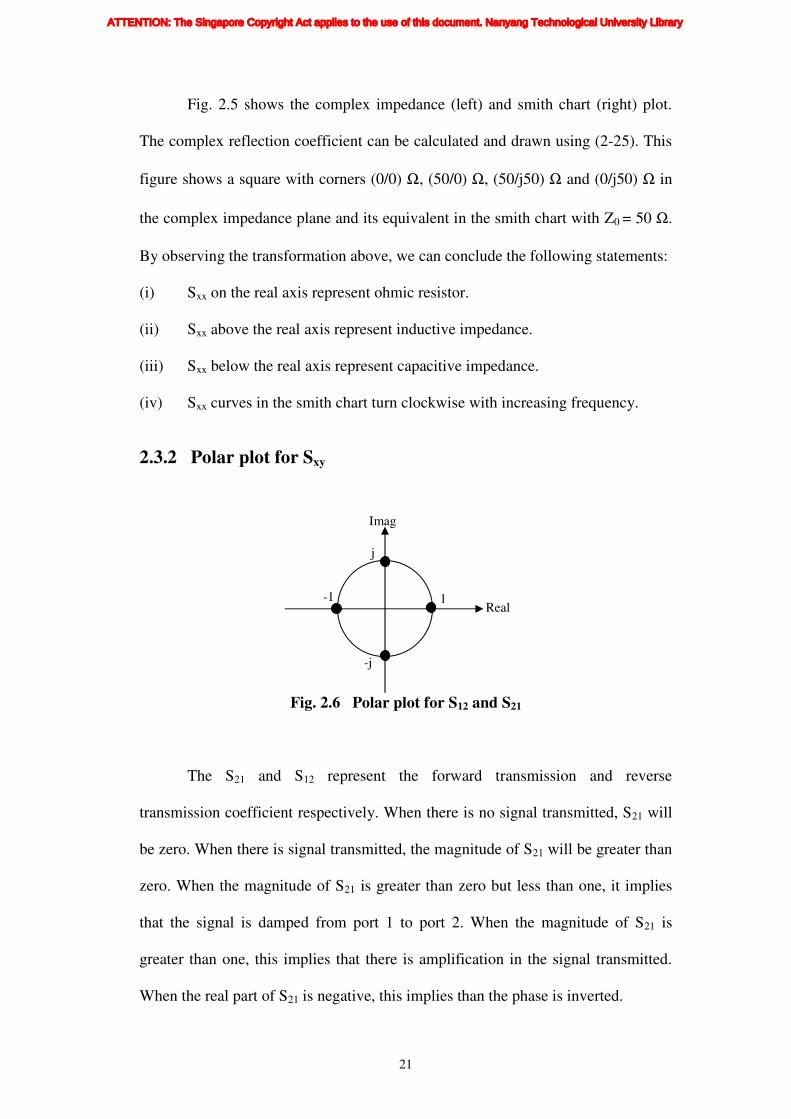
Fig. 2.5 shows the complex impedance (left) and smith chart (right) plot.
The complex reflection coefficient can be calculated and drawn using (2-25). This
figure shows a square with corners (0/0) Ω, (50/0) Ω, (50/j50) Ω and (0/j50) Ω in
the complex impedance plane and its equivalent in the smith chart with Z0 = 50 Ω.
By observing the transformation above, we can conclude the following statements:
(i) Sxx on the real axis represent ohmic resistor.
(ii) Sxx above the real axis represent inductive impedance.
(iii) Sxx below the real axis represent capacitive impedance.
(iv) Sxx curves in the smith chart turn clockwise with increasing frequency.
2.3.2 Polar plot for Sxy
Fig. 2.6 Polar plot for S12 and S21
The S21 and S12 represent the forward transmission and reverse
transmission coefficient respectively. When there is no signal transmitted, S21 will
be zero. When there is signal transmitted, the magnitude of S21 will be greater than
zero. When the magnitude of S21 is greater than zero but less than one, it implies
that the signal is damped from port 1 to port 2. When the magnitude of S21 is
greater than one, this implies that there is amplification in the signal transmitted.
When the real part of S21 is negative, this implies than the phase is inverted.
Imag
Real
j
-j
-1 1
ATTENTION: The Singapore Copyright Act applies to the use of this document. Nanyang Technological University Library

22
Note than the parameter Sxy will turn in the clockwise direction with
increasing frequency.
2.4 Unity Short-Circuited Current Gain and Unilateral
Power Gain Frequency
2.4.1 Unity short-circuited current gain frequency (fT)
fT is defined as the frequency when the short-circuited current gain of the
device drops to unity.
0
2=
=−Vi
igaincurrentcircuitedShort
in
out (2-26)
For a simplified small-signal model for a MOSFET, the short-circuited
current gain is derived as in (2-27).
)( gdgs
m
in
inm
in
out
CCj
g
i
vg
i
i
+==
ω (2-27)
By substituting (2-27) to be equal to one, the parameter fT is derived and
shown in (2-28).
)(**2 gdgs
mT
CC
gf
+=
π (2-28)
From (2-17), it is found that the parameter H21 is actually equivalent to the
short-circuited current gain and by performing a conversion from the de-embedded
S-parameters to H-parameters, the calculated H21 can be used for the extraction of
fT.
Basically, fT can be extracted by either the direct measurement or the
extrapolation method. The direct measurement method is only possible when the
device’s fT is lower than the measurement tool limitation. Hence, by directly
ATTENTION: The Singapore Copyright Act applies to the use of this document. Nanyang Technological University Library
23
measuring the S-parameters and converting it to the H-parameters, the calculated
H21 parameter can be used for the extraction of fT. When the device’s fT is larger
than the measurement tool limitation, the extrapolation method is used for the
extraction. In the extrapolation method, the H21 parameter versus frequency plot is
extrapolated at a frequency point where it observed a -20 dB/decade and the
intercept of the frequency axis is equivalent to fT.
2.4.2 Unilateral power gain frequency (fMAX)
fMAX is defined as the frequency when the unilateral power gain is
equivalent to one and it is given as follows,
GDGTGds
T
MAXCRfRg
ff
π22 += (2-29)
Unilateral power gain can be obtained when the input of the transistor is
conjugate-matched to the input signal source and the load is also conjugate-
matched to the transistor’s output impedance, and an appropriate network is used
to cancel off the effect of feedback from the output to the input. It is given as
shown in (2-30) and (2-31). Note that the parameter k is known as the stability
coefficient.
−⋅
−⋅
=
12
21
12
21
2
12
21 15.0
S
Sreal
S
Sk
S
S
gainpowerUnilateral (2-30)
( )
2112
2
21122211
2
22
2
11
2
1
SS
SSSSSSk
⋅⋅
⋅−++−−= (2-31)
Similarly, fMAX can be extracted by direct or extrapolation method. The
measurement tools limitation will limit which method to use for the fMAX
ATTENTION: The Singapore Copyright Act applies to the use of this document. Nanyang Technological University Library
24
extraction. Note that at low frequency, the unilateral power gain is usually unstable
and hence, fMAX should only be extrapolated at higher frequency region.
2.5 Types of Noise in Transistor
2.5.1 Thermal noise
Thermal noise is also known as Johnson [37] or Nyquist [38] noise and it is
explained by the Brownian motion of thermally agitated charge carriers that
generally move in random direction and generate a randomly varying current or
voltage. The amount of noise is usually characterized in terms of mean square or
root mean square values. The thermal noise is quantified by the available noise
power (PNA) as shown in (2-32), where k is the Boltzmann’s constant (1.38 x 10⁻²³
J/K), T is the absolute temperature in Kelvins and ∆f is the noise bandwidth in
Hertz [39].
fkTPNA ∆= (2-32)
From (2-32), the available noise power of the thermal noise is frequency
independent and it increases with the temperature or the noise bandwidth. Note
that thermal noise is also commonly known as white noise.
2.5.2 Shot noise
Shot noise normally occurs in diode and bipolar transistor. It is generated
when the charge carriers cross potential barriers randomly with a DC current flow.
The total DC current flow and bandwidth affect the noise spectral density of shot
noise as shown in (2-33)
fqIin ∆= 22 (2-33)
ATTENTION: The Singapore Copyright Act applies to the use of this document. Nanyang Technological University Library
25
where 2
ni is the root mean square noise current , q is the electronic charge (1.6 x
10-19
C), I is the DC current value in amperes and ∆f is the noise bandwidth in
Hertz [39].
Note that the shot noise also appears to be frequency independent as with
the thermal noise.
2.5.3 Generation and recombination noise
In the semiconductor structure, there are traps and recombination centers in
the lattice. When the free electrons move randomly in the semiconductor structure,
the continuous trapping and de-trapping process of free electrons generate a
fluctuation in the number of charge carrier per unit time. The fluctuation of the
charge carriers affect the conductance of the semiconductor and in turn generate a
fluctuation of the current flowing through it. The noise generated from this kind of
mechanism is known as the generation and recombination noise.
2.5.4 Flicker noise
Many theories have been presented to explain the flicker noise behavior.
The two main theories are the random fluctuation of the carriers in the channel
[40]-[43] and mobility fluctuation [44], [45]. Based on the carrier fluctuation [42],
[43] and mobility fluctuation [44], [45] theory, the noise voltage power spectral
density can be shown as in (2-34) and (2-35) respectively. Note that K1 in (2-34) is
bias independent while in (2-35), K(VGS) is a bias dependent parameter. Their
corresponding noise current power spectral density can be found using (2-36).
c
gtotalox
vg
fLWC
KS
112
1
⋅= (2-34)
ATTENTION: The Singapore Copyright Act applies to the use of this document. Nanyang Technological University Library
26
fLWC
VKS
gtotalox
GSvg
11)(
⋅= (2-35)
vgmid SgS ⋅= 2 (2-36)
2.5.5 Noise parameters and linear two-port noise theory
Before the noise parameters and noise theory are discussed, it is important
for us to be clear of the definition for some basic noise terms. Noise figure (NF) is
defined as the signal to noise ratio at the input divided by the signal to noise ratio
at the output and it is used as a measure on the noise performance of a transistor or
a whole circuit block. The parameter NF is governed by the famous noise equation
as given in (2-37) and it basically consists of three noise parameters, namely the
minimum noise figure (NFmin), the normalized noise resistance (rn) and the
optimum source reflection coefficient (Γopt). Note that Γs is the input source
reflection coefficient. The parameter NFmin is defined as the minimum noise figure
achievable when Γs is matched to Γopt and rn is defined as the normalized noise
resistance (normalized to 50 Ω) that shows the rate of change of NF with respect to
the mismatched between Γs and Γopt. From (2-37). By knowing the three noise
parameters and the input source reflection coefficient the transistor or system’s NF
can be calculated. Note that Γopt is a complex number and hence it has both the real
and imaginary part. Therefore, the number of noise parameters is sometimes
referred as the four noise parameters.
( ) 22
2
min
11
4
opts
optsnrNFNF
Γ+⋅Γ−
Γ−Γ+= (2-37)
ATTENTION: The Singapore Copyright Act applies to the use of this document. Nanyang Technological University Library

27
In [46], it is shown that a noisy two-port network can be represented using
a noiseless two-port network with two noise current sources as shown in Fig.
2.7(a) and these two noise current sources are usually correlated.
(a)
(b)
Fig. 2.7 Noisy two-port network representation
By utilizing the Y-parameters and the noise current sources i1, i2 and their
correlation term *
21 ii in Fig. 2.7(a), its equivalent two-port network in Fig. 2.7(b)
with a noise voltage and current source can be derived. By converting to the noise
source representation as shown in Fig. 2.7(b), the noise parameters can be easily
derived from a single frequency measurement of the two-port noise factor as a
function of input mismatch [47]. In [46], the method to extract i, u and Ycor in Fig.
2.7(b) was reported as follows.
corun Yuii ⋅+= (2-38)
2*
uYui cor=⋅ (2-39)
u Noiseless
Two-port
Network i
i2
Noiseless
Two-port
Network i1
ATTENTION: The Singapore Copyright Act applies to the use of this document. Nanyang Technological University Library

28
2
21
1i
Yu −= (2-40)
2
21
111 i
Y
Yii −= (2-41)
corcorcor jBG
i
iiYYY +=−=
2
2
*
212111 (2-42)
Based on the above equations, the noise power of u and i can be derived as
follows,
ufRkTY
iu ∆== 4
2
21
2
22 (2-43)
ifGkTY
Yii
Y
Yiii ∆=
−+= 4Re2
*
21
*
11*
21
2
21
112
2
2
1
2 (2-44)
From (2-41) to (2-42), the noise parameters can be calculated as shown in [46].
un RR = (2-45)
2
cor
n
i
opt BR
GG −= (2-46)
coropt BB −= (2-47)
( )optcorn GGRNF +⋅+= 21min (2-48)
Note that Gopt and Bopt are defined as the optimum source conductance and
susceptance respectively.
2.6 Summary
The Y, Z and H parameters were discussed and studied. Due to the various
difficulties to measure the Y, Z and H parameters at RF frequency, S-parameters
are used to characterize the RF devices. The S-parameters can be obtained by
ATTENTION: The Singapore Copyright Act applies to the use of this document. Nanyang Technological University Library

29
supplying a signal at port 1 and monitor the transmitted and reflected signal at port
2 and port 1 respectively. The S-parameters is not unique for RF circuit; it can be
easily converted to Y, Z or H parameters if required. The definition and extraction
methods for fT and fMAX are presented. The different types of noise that exist in the
semiconductor are also given. The definition of the noise parameters and the linear
two-port noise theory are presented and discussed.
ATTENTION: The Singapore Copyright Act applies to the use of this document. Nanyang Technological University Library

30
Chapter 3
DEVICE CHARACTERIZATION
3.1 Introduction
Device characterization is a very important process for RF device
modeling. The inaccuracy of the characterization results will introduce additional
error in the developed models. When performing circuit simulation with these
models, inaccurate simulation results are produced that can cause fabricated
circuits fail to meet their electrical specifications. Therefore, it is very critical to
have the necessary knowledge on how to obtain accurate device characterization
results. The process of device characterization involves the DC, low and high
frequency test measurements, the device layout and the pads and interconnects
structure design. In order to achieve accurate device characterization, measurement
system calibration must be done to remove the parasitic that exist in the
measurement system. By shifting of the measurement reference plane with the
various reported de-embedding techniques, the intrinsic device’s performance can
be extracted.
3.2 DC Measurement
During DC measurement, the parameter analyzer such as the HP4156C and
HP4142 are commonly used to measure the device’s DC curves. The source
monitor unit (SMU) in the parameter analyzer can force voltage or current and
measure the resultant current or voltage at the probe terminal with good resolution
and accuracy. The probing used for the measurement is normally a low leakage
single pin probe that is Kelvin-connected so as to remove the parasitic resistances
ATTENTION: The Singapore Copyright Act applies to the use of this document. Nanyang Technological University Library

31
from the SMU, cables and connectors. Depending on the test structure design,
sometimes RF probes can be used for the DC measurement when the measurement
difference is small as compared to the DC probes. During low current
measurement, high resolution SMU (HRSMU) and longer integration are required
for more accurate measurement. For measurement of large current flow, medium
power SMU (MPSMU) and shorter integration time can be used to reduce the
measurement time without compromising the accuracy of the measurement. For
very large current flow that exceeds the current compliance of the HRSMU and
MPSMU, the high power SMU (HPSMU) can be used for the measurement. The
maximum current compliance for both of the HRSMU and MPSMU is 0.1 A while
the HP-SMU it is 1 A. Note that when measuring large current flow, heating of the
device and the current path will occur that will increase the parasitic resistance in
the current path. Hence, pulse IV measurement system maybe require to prevent
the device and instrument from heating up and change the intrinsic DC
characteristics.
3.3 RF Measurement
As the RF measurement sweep for a range of frequency and biasing points,
the time require for this kind of measurement is usually very much longer than the
DC measurement case. Hence to prevent wasting of the precious measurement
time to measure a “dead” device, its DC curves are measured first to ensure that
the device is working before starting the RF measurement.
ATTENTION: The Singapore Copyright Act applies to the use of this document. Nanyang Technological University Library

32
3.3.1 S-parameter measurement system
Fig. 3.1 S-parameter measurement system
Fig. 3.1 shows the complete system for the S-parameter measurement. The
function of each block is described as follows.
HP8510 network analyzer is used as a control and display unit of the
measurement system. It controls the setting of the AC signal power, attenuation
level and many others setting. It also allows the display to change to any of the
display settings available in the box. During the measurement setup, it is always
very difficult to decide the level of AC signal power to supply to the DUT. There
are two possible scenarios that may occur when the signal power level is set too
low. Firstly the signal source is not ideal; thus it has a certain frequency response.
At higher frequency range, the signal power will start to drop and this will cause
HP8510 Network
Analyzer
HP8341B RF
Synthesizer
S-parameter test set
Probe station
Bias TEE DUT
Bias TEE
HP4156 DC Bias
Port 1 Port 2
HPIB Signal flow
ATTENTION: The Singapore Copyright Act applies to the use of this document. Nanyang Technological University Library

33
calibration issue and inaccurate measurement as the supplied power is not set at the
specified level at higher frequency range. Secondly, the S-parameters when
measured at low signal power setting will be coupled with very high noise and the
measured data will not be “clean”. When the signal power is set too high, non-
linear distortion and gain compression may occur and cause the measured S-
parameters to be inaccurate. Therefore, there are two ways to determine the signal
power level for RF measurement. Firstly, by measuring the S-parameters for a
range of power level setting and when the S-parameters are almost unchanged with
the change in power level setting, that range of power level setting can be used for
the measurement. Secondly, when the DC curves are measured with the signal
source turns on, if the signal power level is set too high, it will affect the measured
Rout versus Vd and Gm vs Vg plots. Therefore, by tuning the power level setting until
the measured DC plots remain unchanged; this power level setting can be used for
the RF S-parameter measurement. Although the attenuation setting can be used to
reduce the signal power level, it is also not an ideal attenuator. Hence, it will
observe a behavior change when frequency increases. Therefore, in order to tackle
the problem with signal power change with frequency, HP8510 provides a power
slope setting whereby the source signal power can be vary when frequency
increases.
The HP8341B RF synthesizer is basically a high frequency signal generator
that provides the signal power to the DUT. By supplying the signal power to the
input and output terminals, the forward and reverse transmission gain or loss and
the input and output impedance can be measured.
ATTENTION: The Singapore Copyright Act applies to the use of this document. Nanyang Technological University Library

34
The S-parameter test set is used to acquire the input and reflected signal
power at the DUT for both ports. It is controlled by HP8510 so that all the four S-
parameters can be measured without having to physically reversing the DUT.
The bias-T is used to couple the AC signal and DC bias to the DUT. It
consists of an inductor and a capacitor in the DC and AC signal path respectively.
The inductor serves like a RF choke that allows only the AC signal to pass through
while the capacitor will block the DC component in its path.
3.3.2 Network analyzer calibration
The purpose of performing network analyzer calibration is to move the
reference plane directly from the network analyzer terminals to the probe pins and
by doing so, all the errors contributed by the measurement system, cables, bias-T
and probe pins can be removed. There are many different calibration techniques
available for the network analyzer. They are the Short-Open-Load-Thru (SOLT),
Thru-Reflection-Line (TRL), Line-Reflection-Match (LRM) and Line-Reflect-
Reflect-Match (LRRM) and the associated error correction calculations. For the
different calibration procedures, the known specific standard terminations have to
be measured. In our measurement, LRRM technique was used as it can provide
high performance calibration with fixed probe separation. In addition, the
calibration process is simple and automated.
ATTENTION: The Singapore Copyright Act applies to the use of this document. Nanyang Technological University Library
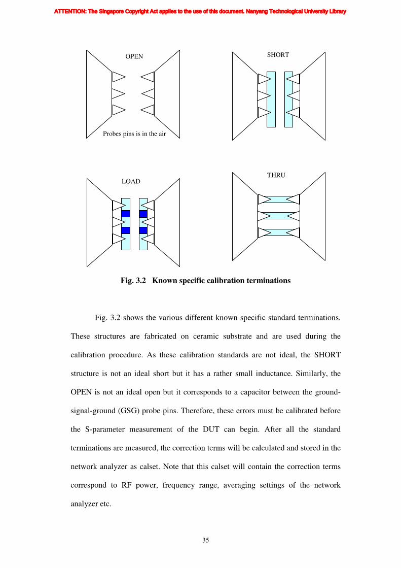
35
Fig. 3.2 Known specific calibration terminations
Fig. 3.2 shows the various different known specific standard terminations.
These structures are fabricated on ceramic substrate and are used during the
calibration procedure. As these calibration standards are not ideal, the SHORT
structure is not an ideal short but it has a rather small inductance. Similarly, the
OPEN is not an ideal open but it corresponds to a capacitor between the ground-
signal-ground (GSG) probe pins. Therefore, these errors must be calibrated before
the S-parameter measurement of the DUT can begin. After all the standard
terminations are measured, the correction terms will be calculated and stored in the
network analyzer as calset. Note that this calset will contain the correction terms
correspond to RF power, frequency range, averaging settings of the network
analyzer etc.
OPEN SHORT
LOAD
Probes pins is in the air
THRU
ATTENTION: The Singapore Copyright Act applies to the use of this document. Nanyang Technological University Library

36
When the S-parameter of the DUT is measured, the data will have to be
corrected inside the network analyzer using the calset and then transfer to the
modeling software and display there.
3.3.3 Probe configuration and device layout
The probe used for the RF measurement is the ground-signal-ground
(GSG) RF probe with pitch size of 100 µm.
Fig. 3.3 RF GSG probes used in measurement
From Fig. 3.3, the three probe tips are in-line and spaced 100 µm apart. The
two outer pins are mainly for grounding while the center pin is the signal pin. Note
that before the calibration process of the network analyzer, the GSG probe must be
checked to ensure that all the probe tips are in-line. Secondly, by tuning the
manipulator, the probe pins must be aligned horizontally so that all the three pins
100 µm
G
G
G
G
S S PORT 1
PORT 2
ATTENTION: The Singapore Copyright Act applies to the use of this document. Nanyang Technological University Library

37
will be in contact with the bond pads at the same time. Thirdly, make sure that all
the three pins can provide a “good” contact on the bond pads before the
measurement begins.
The RF MOSFET used in the measurement is processed by 0.18 µm, 0.25
µm and 90 nm technology. Multi-finger configuration was used for the transistor to
reduce the gate resistance so that lower noise and higher fMAX can be achieved.
Substrate contacts are also implemented to protect the whole transistor so as to
improve the noise performance. Fig. 3.4 shows an example of the RF transistor
layout design.
Fig. 3.4 RF transistor layout design
ATTENTION: The Singapore Copyright Act applies to the use of this document. Nanyang Technological University Library

38
3.3.4 De-embedding methods
During high frequency measurement, the parasitic from the bond pads and
interconnect lines must be de-embedded to obtain the intrinsic DUT
characteristics. The two most widely used methods are the OPEN and OPEN-
SHORT de-embedding technique.
Dummy structures are layout to have only the bond pads and interconnect
lines but without any active implant. These dummy structures are used to de-
embed the parasitic that comes from the bonding pads and interconnect lines.
3.3.4.1 OPEN de-embedding
OPEN de-embedding is the simplest way to de-embed the parasitic and is
often used for frequency range up to 10 GHz. In this method, the impedance of all
the parasitic series resistance and inductance are assumed to be negligible for
frequency less than 10 GHz.
Fig. 3.5 OPEN structure layout and its equivalent circuit
Fig. 3.5 shows the physical layout and its equivalent circuit with the DUT.
The resistance Rp1 and Rp2 represent the ohmic losses due to the silicon substrate.
DUT
Rp1 Rp2
Cp1 Cp2
Cp3
PORT1 PORT2
Layout Equivalent circuit
ATTENTION: The Singapore Copyright Act applies to the use of this document. Nanyang Technological University Library

39
Cp1 and Cp2 represent the coupling capacitance between the signal and ground
pads. Cp3 represents the coupling capacitance between the signal pad at port 1 and
signal pad at port 2. The S-parameters for the OPEN structure are measured and
converted to Y-parameters and manipulated as below:
OPENTOTALDUT YYY −= (3-1)
)( DUTDUT YSS = (3-2)
YTOTAL represents the Y-parameters that include both the DUT and open
parasitic while YOPEN represents the Y-parameters that include only the OPEN
structure. SDUT represents the S-parameters of the DUT only.
3.3.4.2 OPEN-SHORT de-embedding
OPEN-SHORT de-embedding is another de-embedding technique that can
be use if the accuracy of the OPEN de-embedding method is not enough. It is
normally used for frequency range above 10 GHz.
Fig. 3.6 SHORT structure layout and its equivalent circuit
Layout
DUT
Rp1 Rp2
Cp1 Cp2
Cp3
PORT1 PORT2
Equivalent circuit
Rs1 Rs2
Rs3
Ls1
Ls3
Ls2
ATTENTION: The Singapore Copyright Act applies to the use of this document. Nanyang Technological University Library

40
Fig. 3.6 shows the physical layout and its equivalent circuit of the DUT.
The parallel parasitic has the same meaning as in the OPEN structure. The
resistances Rs1, Rs2 and Rs3 represent the ohmic losses of the interconnect lines.
Ls1, Ls2 and Ls3 represent the parasitic inductance of the interconnect lines. The
S-parameters for both the OPEN and SHORT structure are measured and
manipulated as below:
Step 1: De-embed from OPEN structure
OPENTOTALOPENDUT YYY −=/ (3-3)
OPENSHORTOPENSHORT YYY −=/ (3-4)
Step 2: Convert to Z parameters
)( // OPENDUTOPENDUT YZZ = (3-5)
)( // OPENSHORTOPENSHORT YZZ = (3-6)
Step 3: De-embed from SHORT structure
OPENSHORTOPENDUTDUT ZZZ // −= (3-7)
Step 4: Convert to S-parameters
)( DUTDUT ZSS = (3-8)
In steps 1 and 2, the OPEN parasitic are de-embedded for both the
“SHORT” and “DUT + OPEN and SHORT parasitic”.
In step3, the “SHORT without OPEN parasitic” is then de-embedded for
the “DUT without OPEN parasitic”.
Finally in step 4, the “DUT without both OPEN and SHORT parasitic” are
converted back to S-parameters to get the intrinsic transistor performance.
ATTENTION: The Singapore Copyright Act applies to the use of this document. Nanyang Technological University Library
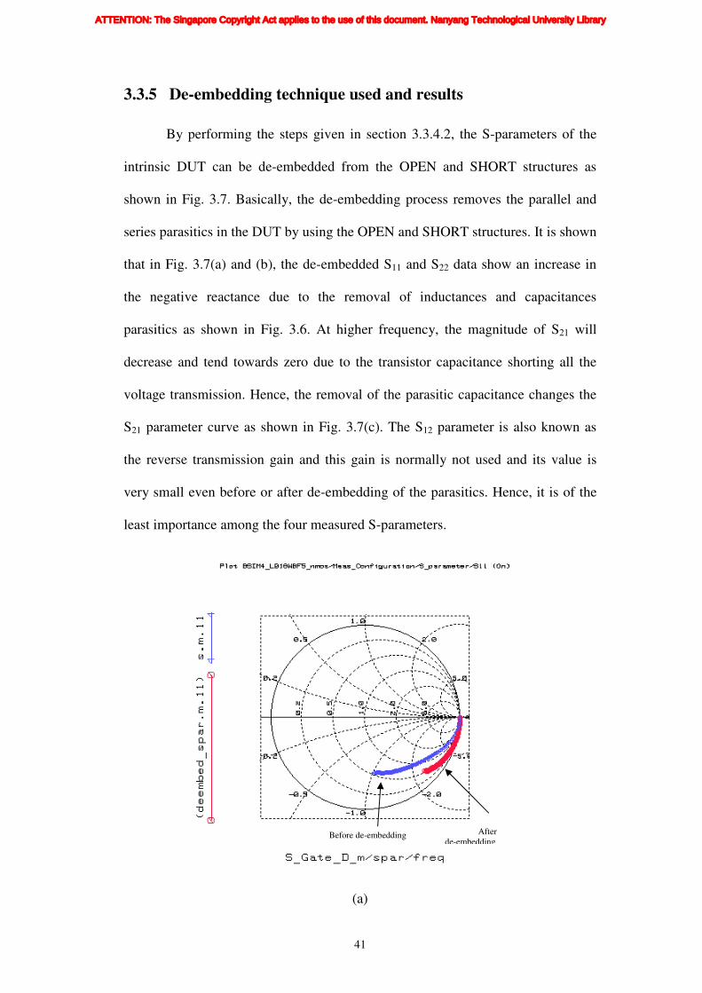
41
3.3.5 De-embedding technique used and results
By performing the steps given in section 3.3.4.2, the S-parameters of the
intrinsic DUT can be de-embedded from the OPEN and SHORT structures as
shown in Fig. 3.7. Basically, the de-embedding process removes the parallel and
series parasitics in the DUT by using the OPEN and SHORT structures. It is shown
that in Fig. 3.7(a) and (b), the de-embedded S11 and S22 data show an increase in
the negative reactance due to the removal of inductances and capacitances
parasitics as shown in Fig. 3.6. At higher frequency, the magnitude of S21 will
decrease and tend towards zero due to the transistor capacitance shorting all the
voltage transmission. Hence, the removal of the parasitic capacitance changes the
S21 parameter curve as shown in Fig. 3.7(c). The S12 parameter is also known as
the reverse transmission gain and this gain is normally not used and its value is
very small even before or after de-embedding of the parasitics. Hence, it is of the
least importance among the four measured S-parameters.
(a)
Before de-embedding After
de-embedding
ATTENTION: The Singapore Copyright Act applies to the use of this document. Nanyang Technological University Library

42
(b)
(c)
Before de-embedding
After de-embedding
Before de-
embedding
After de-
embedding
ATTENTION: The Singapore Copyright Act applies to the use of this document. Nanyang Technological University Library

43
(d)
Fig. 3.7 Comparison of the S-parameters before and after de-embedding of
the OPEN and SHORT structure
3.4 Flicker Noise Measurement and Test Structure
Flicker noise mainly affects the low frequency performance of the
transistor but the impact of flicker noise cannot be neglected in certain RF circuits
such as mixer and oscillator because it can up-convert the low frequency noise to
high frequency that can affect the circuit’s phase noise performance [48]. For
example, the low frequency noise in the current source of a VCO can be up-
converted and appears as phase noise. Poor phase noise will directly affect the
transceiver’s bit error rate (BER) and its adjacent channel rejection performance.
Therefore, it is important to study the flicker noise behavior of the RF transistor.
Furthermore, in order to perform the high frequency noise modeling of the RF
transistor, the parasitic resistances and the flicker noise of the transistor has to be
Before de-embedding
After de-embedding
ATTENTION: The Singapore Copyright Act applies to the use of this document. Nanyang Technological University Library
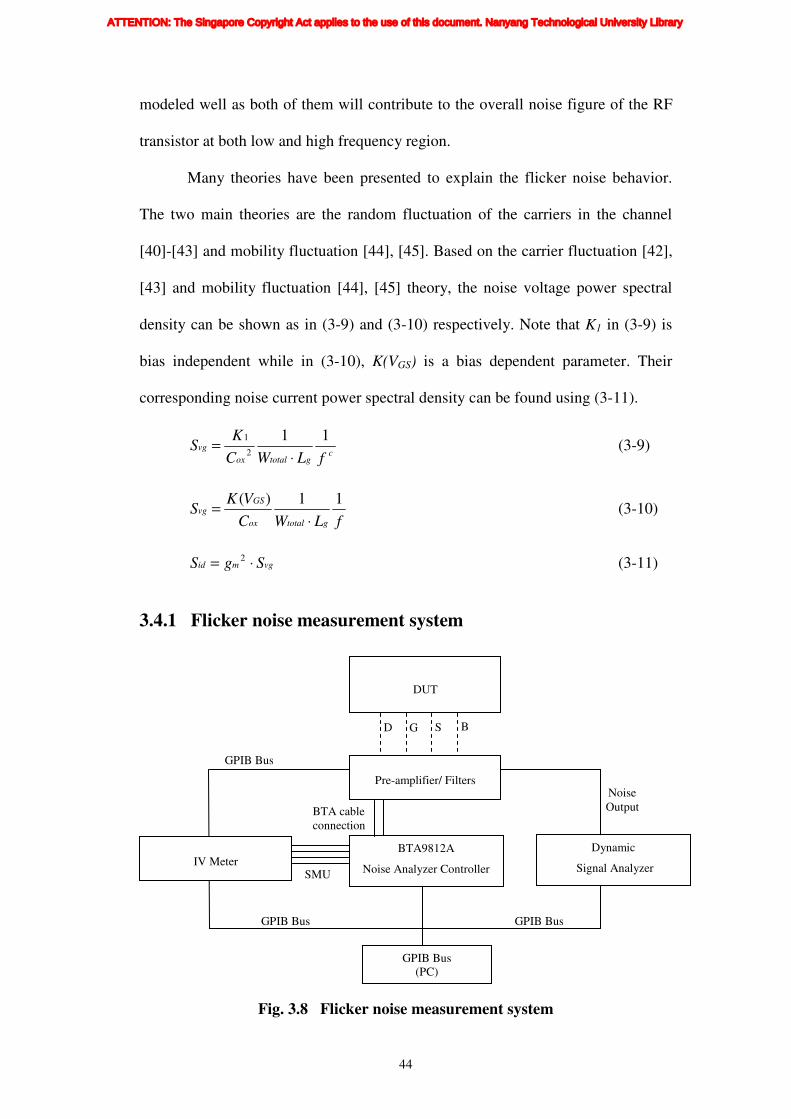
44
modeled well as both of them will contribute to the overall noise figure of the RF
transistor at both low and high frequency region.
Many theories have been presented to explain the flicker noise behavior.
The two main theories are the random fluctuation of the carriers in the channel
[40]-[43] and mobility fluctuation [44], [45]. Based on the carrier fluctuation [42],
[43] and mobility fluctuation [44], [45] theory, the noise voltage power spectral
density can be shown as in (3-9) and (3-10) respectively. Note that K1 in (3-9) is
bias independent while in (3-10), K(VGS) is a bias dependent parameter. Their
corresponding noise current power spectral density can be found using (3-11).
c
gtotalox
vg
fLWC
KS
112
1
⋅= (3-9)
fLWC
VKS
gtotalox
GSvg
11)(
⋅= (3-10)
vgmid SgS ⋅= 2 (3-11)
3.4.1 Flicker noise measurement system
Fig. 3.8 Flicker noise measurement system
DUT
Pre-amplifier/ Filters
BTA9812A
Noise Analyzer Controller
GPIB Bus
(PC)
GPIB Bus
D G S B
BTA cable
connection
IV Meter SMU
Dynamic
Signal Analyzer
Noise
Output
GPIB Bus GPIB Bus
ATTENTION: The Singapore Copyright Act applies to the use of this document. Nanyang Technological University Library

45
Fig. 3.8 shows the flicker noise measurement system. The function of each
block is described as follows.
NoisePro [49] is the window based flicker noise measurement software that
is installed in the PC. By entering all the measurement and extraction settings into
the measurement software, it can send and receive information to the rest of the
measurement instruments via the general purpose interface bus (GPIB) cables.
The software allows both the DC and flicker noise measurement to be performed
on the DUT and it is able to extract and simulate the flicker noise model
parameters to obtain the noise spectral density of the DUT.
IV meter such as the HP4142B or Agilent 4156C parameter analyzer [50]
are used to provide the DC biasing supply required by the DUT with the source
measurement unit (SMU). The SMU is able to source and monitor the voltage or
current flowing through the terminal so that biasing condition of the DUT can be
known during the flicker noise measurement process.
BTA9812A noise analyzer [51] has a detachable pre-amplifier and filter
unit which can be placed closer to the DUT in the measurement chamber. The pre-
amplifier is battery operated for optimal low noise measurement. The biasing
voltage supply from the IV meter will contain noise and they are being filtered off
by the RC filters in the detachable unit. RC filters are used to avoid causing
instability problems of the SMUs. By changing the resistor in each filter, the time
constant of the filter can be changed. Long filter time constant will produce more
accurate noise measurement but the time required for the noise measurement will
be larger due to longer filter response time and settling time required to wait for
the filter’s output to be stabilized. The pre-amplifier contains both the voltage and
ATTENTION: The Singapore Copyright Act applies to the use of this document. Nanyang Technological University Library

46
current noise amplifier. In general DUTs with low output resistance should be
measured with a voltage amplifier, while DUTs with high output resistance should
be measured with a current amplifier.
The dynamic signal analyzer used in this experiment is SR780 [52]. It is
mainly used to measure the amplified noise signal from the DUT and the measured
noise spectral density is then feedback to the PC host that control the whole
measurement system via GPIB connection [53].
3.4.2 Test structure
As the flicker noise measurement is performed at low frequency region,
typically less than 1 MHz, the parasitics from the bond pads, interconnects and test
structure design will not appear and affect the flicker noise measurement. Hence,
the test structure design for the DUT to be measured for flicker noise can used
either the DC or RF transistor test structure as shown in Fig. 3.9.
(a) (b)
Fig. 3.9 (a) DC and (b) RF transistor test structures
3.4.3 Measurement results
The typical flicker noise measurement results comprise of the measured
DC and noise current spectral density. By simulating the model parameters, the
ATTENTION: The Singapore Copyright Act applies to the use of this document. Nanyang Technological University Library

47
simulated DC and flicker noise results can be obtained and compared with the
measured results. The measured and simulated DC and noise current spectral
density characteristics for the DUT are shown in Figs. 3.10 and 3.11.
0.4 0.82 1.24 1.66 2.08 2.5Vgs (V)
1.0e-7
1.0e-6
1.0e-5
1.0e-4
1.0e-3
Id (
A)
Vds(V)=
0.301.002.50
W/L/T=16/.3/27, Vbs=0V,
0.4 0.82 1.24 1.66 2.08 2.5Vgs (V)
1.0e-6
1.0e-5
1.0e-4
1.0e-3
Gm
(m
ho
)
Vds(V)=
0.301.002.50
W/L/T=16/.3/27, Vbs=0V,
0.3 0.74 1.18 1.62 2.06 2.5Vds (V)
1.0e-7
1.0e-6
1.0e-5
1.0e-4
1.0e-3
Id (
A)
Vgs(V)=
0.400.600.801.001.502.002.50
W/L/T=16/.3/27, Vbs=0V,
0.3 0.74 1.18 1.62 2.06 2.5Vds (V)
1.0e-7
1.0e-6
1.0e-5
1.0e-4
1.0e-3
1.0e-2
Gd
(m
ho
)
Vgs(V)=
0.400.600.801.001.502.002.50
W/L/T=16/.3/27, Vbs=0V,
Fig. 3.10 Measured (symbol) and simulated (solid line) DC results
1.0e0 1.0e1 1.0e2 1.0e3 1.0e4 1.0e5Frequency (Hz)
1.0e-19
1.0e-18
1.0e-17
1.0e-16
1.0e-15
1.0e-14
Sid
(A
²/H
z)
int.=4.2e-10slo.=-0.918Ird=6.6e-4Vrd=2.498
Irg=-1.0e-9Vrg=0.80
Gm=3.5e-3Gd=2.4e-4Rb=0.0e+0Rbf=1.0e+2Rd=1.0e+3Rdf=3.0e+2
Amp=In. Vol.
21-17 W/L/T=16/.3/27 Vgs=.8V, Vds=2.5V, Vbs=0V
1.0e0 1.0e1 1.0e2 1.0e3 1.0e4 1.0e5Frequency (Hz)
1.0e-19
1.0e-18
1.0e-17
1.0e-16
1.0e-15
1.0e-14
Sid
(A
²/H
z)
int.=2.4e-10slo.=-0.784Ird=3.9e-3Vrd=2.494
Irg=-9.9e-10Vrg=1.50
Gm=5.0e-3Gd=4.3e-4Rb=0.0e+0Rbf=1.0e+2Rd=1.0e+3Rdf=3.0e+2
Amp=In. Vol.
21-19 W/L/T=16/.3/27 Vgs=1.5V, Vds=2.5V, Vbs=0V
1.0e0 1.0e1 1.0e2 1.0e3 1.0e4 1.0e5Frequency (Hz)
1.0e-19
1.0e-18
1.0e-17
1.0e-16
1.0e-15
1.0e-14
Sid
(A
²/H
z)
int.=6.8e-10slo.=-0.894Ird=1.5e-3Vrd=2.496
Irg=-1.0e-9Vrg=1.00
Gm=4.5e-3Gd=3.4e-4Rb=0.0e+0Rbf=1.0e+2Rd=1.0e+3Rdf=3.0e+2
Amp=In. Vol.
21-18 W/L/T=16/.3/27 Vgs=1V, Vds=2.5V, Vbs=0V
1.0e0 1.0e1 1.0e2 1.0e3 1.0e4 1.0e5Frequency (Hz)
1.0e-19
1.0e-18
1.0e-17
1.0e-16
1.0e-15
1.0e-14
Sid
(A
²/H
z)
int.=2.6e-10slo.=-0.878Ird=6.4e-3Vrd=2.493
Irg=-9.9e-10Vrg=2.00
Gm=5.1e-3Gd=4.7e-4Rb=0.0e+0Rbf=1.0e+2Rd=1.0e+3Rdf=3.0e+2
Amp=In. Vol.
21-20 W/L/T=16/.3/27 Vgs=2V, Vds=2.5V, Vbs=0V
Fig. 3.11 Measured (red) and simulated (green) noise current spectral
density
ATTENTION: The Singapore Copyright Act applies to the use of this document. Nanyang Technological University Library

48
From (3-9) to (3-11), it is clear that the flicker noise model is strongly
dependent on the model DC characteristics. Therefore, it is expected that the
flicker noise model should be scalable as the DC model in terms of the device
geometry and biasing points. Furthermore, since the flicker noise measurement is
done at low frequency region, the layout parasitic should not come into play and
affect the measured results.
3.5 High Frequency Noise Measurement and Test
Structure
From the classical RF noise model from Van Der Ziel [54], [55], the high
frequency noise of a transistor can be described by two correlated current noise
sources, the drain noise current (ind) and the induced gate noise current (ing). The
induced gate noise is caused by the capacitive coupling from the channel noise
current. The mean-square representation for drain current noise and gate noise are
shown in (3-12) and (3-13) respectively. Note that c is the correlation factor
between the drain and gate noise sources.
fgkTi dnd ∆= 02 4 γ (3-12)
fg
CkTi
d
gsng ∆
=
0
222
54
ωδ (3-13)
22
ndng
ndng
ii
iic
⋅
⋅≡
∗
(3-14)
In (3-12), the parameter gd0 is the drain-source conductance at zero VDS and
γ is the noise factor and has a value of unity at zero VDS, while in long channel
devices, it decreases to a value of 2/3 in saturation region. Note that for short
channel devices operating in the saturation region, γ can be considerably higher
ATTENTION: The Singapore Copyright Act applies to the use of this document. Nanyang Technological University Library
49
than the long channel value. In (3-13), the parameter δ is the gate noise coefficient
and it is given a value of 4/3 in [54].
In [56], [57], the approximated expression for minimum noise factor (Fmin)
is derived as shown in (3-15). In the next section, we will relate this expression to
our measured NFmin parameter. Noted that NFmin is the equivalent of Fmin in decibel
(dB).
( )isgm
c
MAX
MAX
RRRgf
f
RPCRPf
fF
++
+⋅
−++≈
2
min
21
21
(3-15)
fkTg
iP
m
nd
∆=
4
2
(3-16)
fg
CkT
iR
m
gs
ng
∆
=
22
2
4ω
(3-17)
⋅
⋅=
∗
22
Im
ndng
ndng
ii
iiC (3-18)
gs
mc
C
gf
⋅⋅=
π2 (3-19)
The P, R and C noise parameters used in (3-15) are related to the drain and
gate noise current sources as shown in (3-16)-(3-19).
ATTENTION: The Singapore Copyright Act applies to the use of this document. Nanyang Technological University Library

50
3.5.1 High frequency noise measurement system
Fig. 3.12 ATN NP5B noise parameter and S-parameter device
characterization system
Fig. 3.12 shows the ATN NP5B system that is used for the HF noise
parameters and S-parameters measurement. The whole system is basically a
combination of two sub-systems, HP8510C vector network analyzer (VNA)
system and HP8970 noise figure measurement system. The NP5 mainframe is used
as a control to switch between the S-parameters and noise measurement system.
The S-parameters measurement system consists of HP8510C VNA,
HP8517B S-parameter test-set and HP83650B synthesizer. Basically, the VNA
controls the test-set and the synthesizer so that the input and output signal power
can be measured to obtain the S-parameters. The detail discussion of the S-
parameter measurement system can be found in Section 3.3.1 of this thesis.
The noise parameters measurement system consists of HP8970B noise
figure meter and HP8971C noise figure test-set. There are two frequency
ATTENTION: The Singapore Copyright Act applies to the use of this document. Nanyang Technological University Library

51
configuration modules that can be selected during the high frequency noise
measurement. The first frequency module range from 0.3 to 6 GHz and the second
is from 2 to 26.5 GHz. The mainframe controls and drives the external connected
mismatch noise source (MNS) and the remote receiver module (RRM) during the
noise measurement. The internal component connection of the MNS consists of an
electronic solid-state multi-state tuner, bias Tee and RF switches that switch
between the VNA and the noise source connected at the input of the MNS module.
In the RRM module, it has a broadband low noise amplifier (LNA) that will lower
the system noise while amplifying the output signal. Consequently, it provides a
low second stage noise figure for the measurement system that improves the noise
measurement accuracy. It also has a bias Tee and RF switches that allows the
output signal to be connected either to the S-parameter test-set or the noise figure
test-set for measurement.
The DC biasing required by the DUT is supplied from HP4142 DC source
and monitor unit (SMU). All the above instruments are controlled by the PC host
which uses the ATN NP5 system software.
The instrument setting used for the S-parameter measurement system is the
same as the discussion in Section 3.3.1. The only difference is the instrument
settings are entered into the NP5 system software whereby it transfers all these
settings to the instruments through GPIB cables. In order to improve the HF noise
characterization accuracy, it performs more noise figure measurements at different
source impedance states. Therefore, the noise measurement time is usually very
much longer than the S-parameter and DC measurement time. Hence, the number
of measurement points and biasing combinations has to be compromised in order
not to over stress the DUT. Furthermore, it is a common practice to measure the
ATTENTION: The Singapore Copyright Act applies to the use of this document. Nanyang Technological University Library

52
DUT DC characteristics first so that to ensure the DUT is operating normally
before the HF noise measurement commences.
3.5.2 Test structure
Unlike in the flicker noise measurement, the HF noise is performed at 0.3
to 26.5 GHz. At such frequency region, the layout parasitic will come into play and
affect the DUT intrinsic characteristics. Hence, the S-parameters and HF noise are
usually measured in the same RF DUT test structure as shown in Fig. 3.9. As the
layout parasitic from the bond pads and interconnects will contribute to the
measured S-parameters and HF noise measurement, the de-embedding process has
to be done for both measurements to obtain the intrinsic behavior of the DUT.
3.5.3 System calibration and verification
In order to perform accurate S-parameters and HF noise measurement in
the ATN NP5 system, the system calibration as directed by its software has to be
performed in sequence as follows.
1. Input SHORT, OPEN and LOAD (SOL) standards calibration
By connecting a THRU structure in place for the DUT, the S22 parameter
measurement of the NP5 system is performed with the SOL standard at the input
of the MNS module. This will help to find the loss of the MNS module.
2. System noise source gamma calibration
By connecting the noise source to the input of the MNS module and turning
it on and off, the same S22 parameter measurement is performed with the THRU
structure; the reflection coefficient of the noise source can be extracted. This
measured result is used to correct the mismatch of the noise diode.
3. System noise source noise figure calibration
ATTENTION: The Singapore Copyright Act applies to the use of this document. Nanyang Technological University Library

53
This calibration determines the system noise figure from the noise diode
contribute back into the system. If any of the noise measurement frequency points
exceed 2 GHz then peaking of the YIG filter is required in this calibration. The
purpose of peaking or fine tuning the YIG filter is to match the pass band response
of the noise figure test-set. However, the peaking of the YIG filter is only required
when the measurement frequency points and range have changed, the noise figure
test-set is turned off or the ambient temperature has varied above ±5 °C since the
last peaking. During the peaking process, it should be observed that the first noise
figure NF1 from the calibration results has to be the lowest.
4. Network analyzer calibration
The network analyzer calibration is actually the S-parameter calibration
and it can utilize any technique supported by the network analyzer or any third
party calibration software. The following techniques such as the Short-Open-Load-
Thru (SOLT), Line-Reflect-Match (LRM), Thru-Reflect-Line (TRL) or Line-
Reflect-Reflect-Match (LRRM) can be used to calibrate the network analyzer.
After the calibration is done, it is advisable to check the calibrated S-parameters
using the known standards from the Impedance Standard Substrate (ISS). By
physically checking the Thru line phase change, the quality of the calibration can
be checked and redo if large phase change is observed when the Thru line is
probed. Note that the reference plane for the S-parameters is the same as the noise
measurement system.
5. Thru line delay calibration
After the network analyzer calibration, the NP5 system will do a Thru line
verification to calculate and display the Thru line delay of 1 pico-second. After this
ATTENTION: The Singapore Copyright Act applies to the use of this document. Nanyang Technological University Library

54
verification, the software system will continue the rest of the noise system
calibration unattended (fully software controlled).
6. RRM calibration
This calibration determines the gamma presented to the DUT at the output
reference plane.
7. MNS calibration
This calibration determines the gamma presented to the DUT at the input
reference plane.
8. Noise parameter calibration
This is the final stage of the noise system calibration. Similar to stages 6
and 7, the calibration runs fully automated. At the end of this calibration stage, the
calibration data is saved and the noise system is ready to perform S-parameter and
HF noise measurements.
Before commencing the HF noise measurement, it is important to verify the
calibration by measuring a known standard or DUT. For example, the Thru line
can be measured for its S-parameters and HF noise. Typically, the loss of a Thru
must be within ±0.1 dB and the NFmin must be within ±0.2 dB. If the above
tolerance is not met, this implies that the S-parameter or the noise calibration is not
done well and require to be redone. Instead of a Thru line, a known passive DUT
such as an attenuator can be measured to verify the system calibration. By
verifying the known standard at the beginning and ending of the measurement
session, the verification results can confirm that the measured noise and S-
parameters are all accurate and reliable. Fig. 3.13 shows an example of a Thru line
measured for its gain and noise parameters at the beginning and ending of the
measurement session and from the measured results, it is clear that the tolerance of
ATTENTION: The Singapore Copyright Act applies to the use of this document. Nanyang Technological University Library

55
the measured Thru line loss and its NFmin values are within specification and this
will assure that all the measured data collected within this measurement session
should be reliable.
Fig. 3.13 Thru line S-parameter and noise verification
3.5.4 High frequency noise de-embedding method
In order to obtain the intrinsic noise performance of a transistor, the pads
and interconnects parasitic that contribute to the overall noise has to be de-
embedded. In this section, the high frequency noise de-embedding method using
the standard OPEN and SHORT structures are presented [58].
Step 1:
Measure the S-parameters of a DUT [SDUT
], OPEN [SOPEN
] and SHORT [SSHORT
]
structure, and convert them to Y-parameters [YDUT
, YOPEN
, YSHORT
] with the below
transformation equation.
±0.1 dB ±0.2 dB
ATTENTION: The Singapore Copyright Act applies to the use of this document. Nanyang Technological University Library

56
[ ]
( )( )( )( )
( )( )[ ]211222110
2112221121
1221122211
11
112
211
SSSSZ
SSSSS
SSSSS
Y−++⋅
+−+−
−++−
= (3-20)
Step 2:
Measure the noise parameters of a DUT [NFminDUT
, YoptOPEN
, RnSHORT
] structure,
and calculate the correlation matrix [CADUT
] with
[ ]( )
−−
−−
=
∗
20
2
12
1
2DUT
opt
DUT
n
DUT
opt
DUT
n
DUT
min
DUT
opt
DUT
n
DUT
minDUT
nDUT
A
YRYRNF
YRNF
RkTC (3-21)
Note that T0 is the standard reference temperature of 290K and the asterisk symbol
denotes the complex conjugate.
Step 3:
Convert the [CADUT
] matrix to its [CYDUT
] with
[ ] [ ][ ][ ]DUTDUT
A
DUTDUT
Y TCTC =†
(3-22)
[ ]
−
−=
0
1
21
11
DUT
DUT
DUT
Y
YT (3-23)
Note that † denotes the Hermitian conjugation of the element.
Step 4:
Calculate the correlation matrix [CYOPEN
] of the OPEN structure with
[ ] [ ]( )OPENOPEN
Y YkTC ℜ= 2 (3-24)
Where k is the Boltzmann constant and T is the absolute temperature.
Step 5:
Subtract the parallel parasitic from [YDUT
] and [YSHORT
]
[ ] [ ] [ ]OPENDUTDUT
I YYY −= (3-25)
[ ] [ ] [ ]OPENSHORTSHORT
I YYY −= (3-26)
ATTENTION: The Singapore Copyright Act applies to the use of this document. Nanyang Technological University Library

57
Step 6:
De-embed [CYDUT
] from the parallel parasitic with
[ ] [ ] [ ]OPEN
Y
DUT
Y
DUT
YI CCC −= (3-27)
Step 7:
Convert the [YIDUT
] and [YISHORT
] to [ZIDUT
] and [ZISHORT
] with
[ ]
−
−
−=
1121
1222
21122211
1
YY
YY
YYYYZ (3-28)
Step 8:
Convert [CYIDUT
] to [CZIDUT
] with
[ ] [ ][ ][ ]DUT
I
DUT
YI
DUT
I
DUT
ZI ZCZC =†
(3-29)
Step 9:
Calculate the correlation matrix [CZISHORT
] of the SHORT structure after de-
embedding the parallel parasitic with
[ ] [ ]( )SHORT
ZI
SHORT
ZI ZkTC ℜ= 2 (3-30)
Note that R() represents the real part of the element.
Step 10:
Subtract the series parasitic from [ZIDUT
] to get the Z-parameters [ZTRANS
] of the
intrinsic transistor with
[ ] [ ] [ ]SHORT
I
DUT
I
TRANSZZZ −= (3-31)
Step 11:
De-embed [CZIDUT
] from the series parasitic to get the correlation matrix with [CZ]
of an intrinsic transistor with
[ ] [ ] [ ]SHORT
ZI
DUT
ZIZ CCC −= (3-32)
Step 12:
ATTENTION: The Singapore Copyright Act applies to the use of this document. Nanyang Technological University Library

58
Convert the [ZTRANS
] of the intrinsic transistor to its chain matrix [ATRANS
] with
[ ]( )
−=
22
2112221111
211
1
Z
ZZZZZ
ZA (3-33)
Step 13:
Transform [CZ] to [CA] with
[ ] [ ][ ][ ]AZAA TCTC =†
(3-34)
[ ]
−
−=
TRANS
TRANS
Aa
aT
21
11
0
1 (3-35)
Step 14:
Calculate the noise parameters of an intrinsic transistor from the noise correlation
matrix in the chain representation [CA] using the following expressions
( ) ( )( )
ℑ−+ℜ+=
2
12221112
0
min
11 AAAA CCCC
kTNF (3-36)
( )( ) ( )( )
A
AAAA
optC
CiCCCY
11
12
2
122211 ℑ+ℑ−= (3-37)
0
11
2kT
CR A
n = (3-38)
Where I() represents the imaginary part of the element and i is the imaginary unit.
3.6 Summary
The various device characterization systems were discussed and presented.
By performing network analyzer calibration, the measurement reference plane can
be moved from the instruments terminals directly to the probe pins. When the
device is measured for its S-parameters, the network analyzer will automatically
remove the contribution from the system and display the measured device
characteristics. In order to obtain the intrinsic device behaviour, the effects from
ATTENTION: The Singapore Copyright Act applies to the use of this document. Nanyang Technological University Library

59
the pads and interconnects has to be removed by using the de-embedding process.
The flicker noise and high frequency noise measurement system are discussed and
presented. The calibration of the high frequency noise system is presented and
verified by measuring the standard THRU structure in the ISS. By performing high
frequency noise de-embedding, the noise contribution from the pads and
interconnect structures can be removed and the intrinsic noise behaviour can be
extracted.
ATTENTION: The Singapore Copyright Act applies to the use of this document. Nanyang Technological University Library

60
Chapter 4
CMOS RF MODELING
4.1 Introduction
In the past, GaAs and bipolar transistors are usually chosen for RF circuits
due to their high unity gain frequency and excellent RF properties. As CMOS
process technology continues to improve, its unity gain frequency has increased to
a level that is comparable to its GaAs and bipolar counterparts. The improved
unity current gain frequency and noise figure of the CMOS transistor coupled with
the lower process cost and higher device integration show that CMOS technology
has great potential in RF applications. In order to build RF circuit using CMOS
devices, accurate and reliable RF CMOS transistor models are required.
In the past, most commercial MOSFET models including the BSIM models
are developed mainly for digital and low frequency analog applications. Through
much effort from the BSIM development team, they have managed to improve the
BSIM model to cater to digital, low frequency and RF modeling requirements. The
recent improvement in BSIM3v3 and BSIM4 RF models demonstrate great
potential in RF transistor modeling.
4.2 RF Parasitic in MOSFET
In the DC and low frequency MOSFET models, the parasitic at the gate
and substrate structures are normally neglected as their effects are usually small in
that frequency range. The source and drain parasitic resistances are also treated as
“virtual” components and are only included to model the voltage drop in the I-V
equation [22]. However, in radio frequency range, the effect of these parasitic can
ATTENTION: The Singapore Copyright Act applies to the use of this document. Nanyang Technological University Library

61
no longer be neglected as they affect quite significantly in the device performance
and must be considered in the equivalent circuit of the device.
4.2.1 Gate resistance modeling
At DC and low frequency range, the gate resistance is seen only as the
poly-silicon sheet resistance. However, at radio frequency range, the effective gate
resistance will change due to the distributed effects observed at the gate terminal
[59]. In order to model the gate resistance accurately at RF, the gate electrode and
the channel must be treated as a distributed structure and their combined resistance
will be the effective gate resistance seen at the gate terminal.
NQSGpolyGG RRR ,, += (4-1)
Fig. 4.1 Distributed effects of the gate electrode and channel
4.2.1.1 Poly-silicon gate electrode resistance (RG,poly)
In [24], the distributed effect of the gate electrode has been studied and the
following equations have been derived to calculate the gate electrode resistance.
N
wLj
N
Lw
wCj
NZ
spoly
p
in
33
/ ωρ
ω++= , Single contacted gate (4-2)
Distributed gate electrode
Source Drain
Gate oxide
Distributed Channel
ATTENTION: The Singapore Copyright Act applies to the use of this document. Nanyang Technological University Library
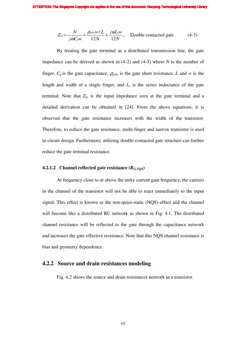
62
N
wLj
N
Lw
wCj
NZ
spoly
p
in
1212
/ ωρ
ω++= , Double contacted gate (4-3)
By treating the gate terminal as a distributed transmission line, the gate
impedance can be derived as shown in (4-2) and (4-3) where N is the number of
finger, Cp is the gate capacitance, ρpoly is the gate sheet resistance, L and w is the
length and width of a single finger, and Ls is the series inductance of the gate
terminal. Note that Zin is the input impedance seen at the gate terminal and a
detailed derivation can be obtained in [24]. From the above equations, it is
observed that the gate resistance increases with the width of the transistor.
Therefore, to reduce the gate resistance, multi-finger and narrow transistor is used
in circuit design. Furthermore, utilizing double-contacted gate structure can further
reduce the gate terminal resistance.
4.2.1.2 Channel reflected gate resistance (RG,NQS)
At frequency close to or above the unity current gain frequency, the carriers
in the channel of the transistor will not be able to react immediately to the input
signal. This effect is known as the non-quasi-static (NQS) effect and the channel
will become like a distributed RC network as shown in Fig. 4.1. The distributed
channel resistance will be reflected to the gate through the capacitance network
and increases the gate effective resistance. Note that this NQS channel resistance is
bias and geometry dependence.
4.2.2 Source and drain resistances modeling
Fig. 4.2 shows the source and drain resistances network in a transistor.
ATTENTION: The Singapore Copyright Act applies to the use of this document. Nanyang Technological University Library

63
Fig. 4.2 Source and drain parasitic resistances network
Basically, the source and drain parasitic consist of via, salicide, contact and
lightly doped drain (LDD) resistances. Normally, the salicide and via resistances
are small when compared to the LDD and contact resistances. Therefore, the LDD
and contact resistances dominant the whole of source and drain parasitic. Since the
LDD resistance is bias dependent, hence the final source and drain resistance will
also experience some biasing effect. But as the channel length continues to scale
down for 0.18 µm technology and below, the LDD doping concentration will
increase with more advance technology. Therefore, the biasing effect on the source
and drain resistance will be diminishing. Assuming that the biasing effect of the
source and drain resistances is negligible, their parasitic resistances can be
represented with (4-4) and (4-5) respectively.
WN
rRR
swSS
*0 += (4-4)
WN
rRR
dwDD
*0 += (4-5)
RS0 and RD0 represent the series resistance components without width
dependence while the rdw and rsw represent the parasitic drain and source
resistances with unit width, respectively.
Gate
Via
resistance
Salicide resistance
Contact resistance
LDD resistance Drain
ATTENTION: The Singapore Copyright Act applies to the use of this document. Nanyang Technological University Library
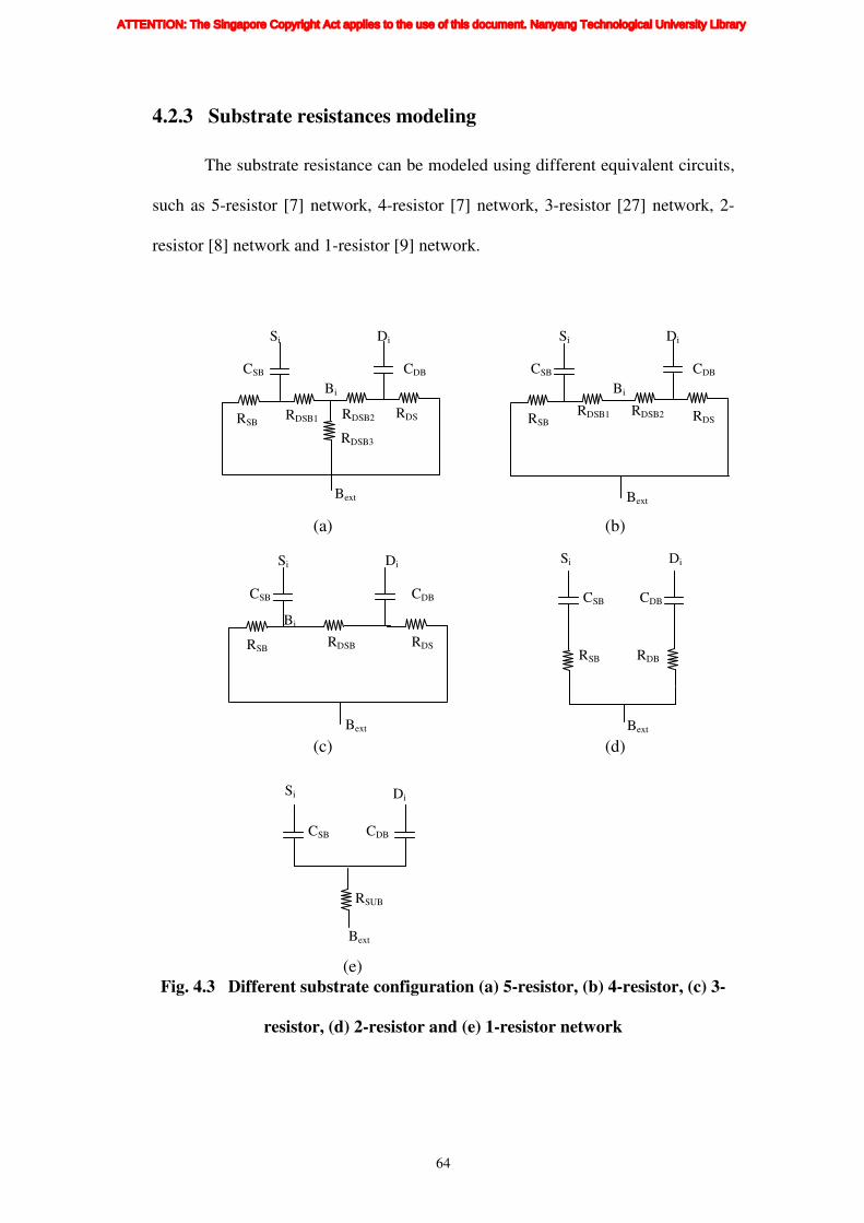
64
4.2.3 Substrate resistances modeling
The substrate resistance can be modeled using different equivalent circuits,
such as 5-resistor [7] network, 4-resistor [7] network, 3-resistor [27] network, 2-
resistor [8] network and 1-resistor [9] network.
(a) (b)
(c) (d)
(e)
Fig. 4.3 Different substrate configuration (a) 5-resistor, (b) 4-resistor, (c) 3-
resistor, (d) 2-resistor and (e) 1-resistor network
Si
Bext
CSB CDB
RSUB
Di
CSB CDB
RSB
Bi
Si Di
RDSB1 RDSB2 RDS
Bext
CSB CDB
RSB
Bi
Si Di
RDSB1 RDSB2 RDS
RDSB3
Bext
CSB CDB
RSB
Bi
Si Di
RDSB RDS
Bext Bext
Si Di
RSB RDB
CSB CDB
ATTENTION: The Singapore Copyright Act applies to the use of this document. Nanyang Technological University Library

65
Fig. 4.3 shows all the five different configuration of the substrate network
reported to characterize the substrate coupling effect at HF region. Due to the
complexity of the parameter extraction and analysis, the 4- and 5-resistor networks
are seldom use in the substrate modeling. The 1- and 2-resistor networks have
fewer components and therefore are easier for parameter extraction but they
become less accurate when operating frequency increases. The 3-resistor network
is a compromise among these networks and can ensure accuracy up to 10 GHz
while maintaining a simple analysis and parameter extraction.
Based on the fact that the depletion region below the gate and surrounding
the source and drain diffusions is dependent on the gate and drain bias condition,
therefore the substrate resistance is also bias dependent [27].
4.2.4 Parasitic capacitances modeling
Fig. 4.4 shows all the parasitic capacitances of a MOSFET and they can be
divided into the following parts:
1) CFO: Outer fringing capacitance between the polysilicon gate and the
source and drain.
2) CFI: Inner fringing capacitance between the polysilicon gate and the source
and drain.
3) CGSO, CGDO and CGBO: Overlap capacitances between the polysilicon gate
and the heavily doped region in the source, drain and bulk. They are
relatively independent of the biasing due to the high doping concentration.
4) CGSL, CGDL: Overlap capacitances between the polysilicon gate and the
lightly doped region in the source and drain. They are dependent on the
biasing due to the lightly doped region in the source and drain.
5) CJS, CJD: Junction capacitances at the source and drain region.
ATTENTION: The Singapore Copyright Act applies to the use of this document. Nanyang Technological University Library

66
6) CSUB: Substrate capacitance.
Fig. 4.4 Parasitic capacitances in MOSFET
Most of the parasitic capacitances are included in the models for digital and
analog application [60]. Although most of the models have already considered the
above parasitic capacitances, additional capacitor can be added as sub-circuit if the
intrinsic capacitance model is not accurate enough to cover for short channel
effects. The substrate capacitance is only considered if the operating frequency is
much higher than 10 GHz.
4.3 BSIM3 – RF Model
To apply the BSIM3v3 model in RF simulation, sub-circuit components
must be added to simulate the parasitic effect [9] as discussed in section 4.2. The
implementation of the BSIM3v3 core model and the sub-circuit components is
known as the macro-modeling approach. As the NQS effect and all the parasitic
Body
Source Drain
Gate
P-sub
n+ n+
CJS CJD
CFO CFO
n- n-
CFI CFI
CGBO
CGSO CGDO
CGSL CGDL
CSUB
ATTENTION: The Singapore Copyright Act applies to the use of this document. Nanyang Technological University Library
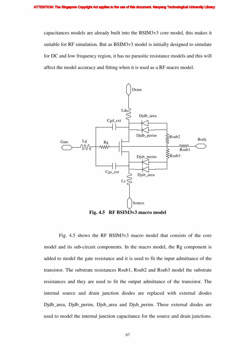
67
capacitances models are already built into the BSIM3v3 core model, this makes it
suitable for RF simulation. But as BSIM3v3 model is initially designed to simulate
for DC and low frequency region, it has no parasitic resistance models and this will
affect the model accuracy and fitting when it is used as a RF macro model.
Fig. 4.5 RF BSIM3v3 macro model
Fig. 4.5 shows the RF BSIM3v3 macro model that consists of the core
model and its sub-circuit components. In the macro model, the Rg component is
added to model the gate resistance and it is used to fit the input admittance of the
transistor. The substrate resistances Rsub1, Rsub2 and Rsub3 model the substrate
resistances and they are used to fit the output admittance of the transistor. The
internal source and drain junction diodes are replaced with external diodes
Djdb_area, Djdb_perim, Djsb_area and Djsb_perim. These external diodes are
used to model the internal junction capacitance for the source and drain junctions.
Rg Lg
Ls
Ld
Cgs_ext
Cgd_ext
Djdb_area
Djsb_area
Djdb_perim
Djsb_perim
Rsub1
Rsub2
Rsub3
Body Gate
Source
Drain
ATTENTION: The Singapore Copyright Act applies to the use of this document. Nanyang Technological University Library
68
The external inductances Lg, Ls and Ld are added to model the terminal
inductance and improve the model fitting if the gate and substrate sub-circuit
components are unable to produce a good fitting model. The Cgs_ext and Cgd_ext
are additional parasitic capacitances that are added if the internal capacitance
model is not adequate to cover short channel effects of the transistor and the
various biasing conditions.
Although the conventional BSIM3v3 macro model can be used to model
RF transistor, its generated RF models are usually valid only for discrete sizes. For
discrete RF models, the number of modeled device sizes is limited and hence
circuit optimization is usually impossible. Furthermore, when a different device
size is needed for the circuit simulation that is not found in the process design kit
(PDK), there is no way to predict the circuit performance using that device size.
Hence, a better modeling approach is required to generate scalable RF models that
can alleviate all the problems of using the conventional approach in transistor
modeling. Furthermore, scalable RF models can be used to build better and
powerful PDK that can shorten the circuit development time and optimize RF
circuit design at the same time. But as the number of device sizes that a scalable
RF model covers is larger, the model verification time will be longer and hence the
conventional way to quantify the accuracy of the developed RF model must be
improved.
ATTENTION: The Singapore Copyright Act applies to the use of this document. Nanyang Technological University Library

69
4.4 BSIM4 – RF Model
Fig. 4.6 BSIM4 RF model
Fig. 4.6 shows the equivalent circuit of a BSIM4 RF model. It includes
both the gate and substrate resistances in its core model so that this model can be
use to run RF simulation.
4.4.1 Gate resistance model
BSIM4 provides several gate resistance configurations so as to provide
greater flexibility in modeling the gate resistance. The selection of the gate
resistance configuration is controlled by the parameter RGATEMOD.
When RGATEMOD = 1, a gate electrode resistance is appended to the
intrinsic transistor gate terminal as shown in the Fig. 4.8. The gate electrode
resistance is given by the following equation:
Gate Rg
Rd
Body
Source
Drain
Rs
Substrate
Resistance
Network
Cjsb
Cjdb
ATTENTION: The Singapore Copyright Act applies to the use of this document. Nanyang Technological University Library

70
( )NFXGLLNGCON
NGCON
WXGWRSHG
R
CJeff
electrodeg
−
+
=3
,
, (4-6)
RSHG represent the gate polysilicon sheet resistance. NGCON is the
number of gate contact for each gate finger; it can be either one if the gate finger is
contacted from only one side or two if the gate finger is contacted at both sides.
XGW is the distance between the gate contact to the channel edge, and XGL is the
difference between the specified L in the MOSFET instance statement and the
physical gate length.
When RGATEMOD = 2, a channel reflected gate resistance Rg,crg is added
to the gate terminal as shown in Fig. 3.8. This Rg,crg is used to model the distributed
RC effect of the channel region and therefore can be described as the first-order
non-quasi-static effect component. Note that this resistance is not a physical
resistance and has no thermal noise. This resistance is given by the following
equation:
+
=
NFCL
W
q
kTXRCRG
V
IXRCRG
R
IVox
eff
effeff
effDS
DS
crgg
.21
1
,'
,
,
µ
(4-7)
Where XRCRG1 and XRCRG2 are used to correct the Rg,crg resistance.
C’ox,IV is the per-area capacitance approximately equal to the C’ox,inv (per unit area
of the oxide capacitance at inversion condition).
The gate resistance configuration for RGATEMOD = 3 is similar to
RGATEMOD = 2 except that the location of the overlap capacitance is different.
ATTENTION: The Singapore Copyright Act applies to the use of this document. Nanyang Technological University Library

71
Fig. 4.7 Geometrical details for the gate terminal in BSIM4 (a) NGCON =1
(b) NGCON = 2
(a)
(b)
L-XGL
Weff.CJ
XGW
G
S D
(a)
XGW
G
S D
(b)
Gate
Cgdo
Drain
Cgso
Source
RGATEMOD = 1
Rg,electrode
Cgso Cgdo
Gate
Source Drain
RGATEMOD = 0
Weff.CJ
ATTENTION: The Singapore Copyright Act applies to the use of this document. Nanyang Technological University Library

72
(c)
(d)
Fig. 4.8 Different gate resistance configuration with respect to RGATEMOD
4.4.2 Substrate resistance model
The substrate resistance network can be activated by the parameter
RBODYMOD. When RBODYMOD = 0, no substrate resistance is generated.
When RBODYMOD = 1, all the five resistances as shown in the Fig. 4.9 are
present simultaneously. A minimum conductance, GBMIN is added in parallel to
all the five resistors. This is to prevent the resistor value from becoming so small
and cause convergence problem to arise.
Gate
Rg,electrode
Cgdo
Drain
Cgso
Source
RGATEMOD = 2
Rg,crg
Gate
Rg,electrode
Cgdo
Drain
Cgso
Source
RGATEMOD = 3
Rg,crg
ATTENTION: The Singapore Copyright Act applies to the use of this document. Nanyang Technological University Library

73
Fig. 4.9 Five-substrate resistances network in BSIM4
The main disadvantage of this substrate network is non-scalability. All the
five-resistors have no geometry dependence and when the transistor size has
changed or the number of finger is changed, all the five resistors value must be
extracted again.
4.5 Summary
All the RF parasitics in a MOSFET are presented and discussed. The RF
models for BSIM3v3 and BSIM4 are also introduced and presented. Although
BSIM3v3 and BSIM4 RF models can be used to model RF transistors, they have
some limitations. Specifically, their generated RF models are usually in discrete
size making circuit optimization is impossible. For those device sizes that are not
modeled or fabricated, the developed discrete RF models cannot be used to predict
the device performance. Some of the model parameters like the substrate network
in BSIM4 have only a fixed value and hence, the developed RF model is not able
to scale for RF simulation. Therefore, there is an urgent need to develop new
scalable RF models for circuit optimization. In parallel with it, new verification
Substrate
RBPB RBDB RBSB
RBPS RBPD
Cjd Cjs
ATTENTION: The Singapore Copyright Act applies to the use of this document. Nanyang Technological University Library

74
techniques must also be developed to improve and shorten the overall scalable
model verification and development time, respectively.
ATTENTION: The Singapore Copyright Act applies to the use of this document. Nanyang Technological University Library

75
Chapter 5
RFCMOS UNIT WIDTH OPTIMIZATION
TECHNIQUE
5.1 Introduction
As CMOS processing technology continues to advance, its radio-frequency
(RF) properties such as unity short-circuit current gain frequency (fT), unilateral
power gain frequency (fMAX) and the noise figure improves [3],[4],[61]-[65]
relentlessly. It has been reported that the fT of a 0.13 µm gate length MOS
transistor can reach 80 GHz region [61]. The down scaling of channel length has
allowed higher integration density and the possibility of integrating digital, analog
and RF circuits into a single chip [66], [67], making CMOS technology a cost
effective solution for fabricating RFIC.
One of the most commonly used components in RF circuit design is the
RFCMOS transistor. In order to optimize the transistor’s RF characteristics, its
layout design methodology has been studied and researched extensively [68]-[72].
Although different foundries, integrated device manufacturers (IDM) and many
fab-less semiconductor companies use various transistor layout designs, typical RF
transistors are designed with multi-fingered and double-contacted gate
configuration. The layout design of the transistor is normally symmetry with
special guard ring added to isolate any interference from other components in the
circuit.
In multi-fingered transistor design, the size of the transistor is mainly
controlled by the finger number (Nf), unit width (Wf) and channel length (Lg) of the
ATTENTION: The Singapore Copyright Act applies to the use of this document. Nanyang Technological University Library

76
transistor. For most RF circuit design, transistors with smallest gate length are
always used due to their fast response and high drain current. Therefore, RF circuit
designer will need to select transistors based on either Nf or Wf. By optimizing per
finger unit width with respect to fT, fMAX, minimum noise figure (NFmin) and flicker
noise, the best Wf of the transistor can be selected to use in a specific circuit
application such as low noise amplifier (LNA), voltage controlled oscillator (VCO)
and mixer. The ability to select and use the optimized layout for the transistor can
ensure that the designed RF circuit produces the best performance at the first
design cycle and this greatly reduces the RF circuit development time. This
methodology when applied to a certain process or technology can help IDM and
foundry select optimal Wf for transistors to optimize circuit performance and also
save large amount of SPICE model development time.
The following figure of merits (FOMs) fT, fMAX, NFmin and flicker noise
spectral density have been commonly used in [65], [68], [73], [74] to characterize
the performance of RFCMOS transistor but these FOMs are normally presented
with respect to the change in technology or channel length. In [69], only the fT
optimization with Wf is shown while in [4] and [72], the fT, fMAX and NFmin
optimization presented were based on large width transistors. Due to transistor’s
parasitic changes with respect to Wf, their effects towards each individual FOM are
different. Hence, it is important to study these four FOMs with respect to Wf on
different transistor sizes so as to obtain an optimized width per finger based on
either one or all the four FOMs.
ATTENTION: The Singapore Copyright Act applies to the use of this document. Nanyang Technological University Library

77
5.2 Design Experiment and Test Structure Layout
In this section, a study on the four FOMs with respect to the transistor’s Wf
is done for small (48 µm), medium (120 µm) and large (240 µm) total width
transistors and a new FOM is proposed for the study of the transistor’s HF noise.
All of the transistor’s fT, fMAX, NFmin and flicker noise spectral density are measured
at the maximum trans-conductance (gm) operating point of the transistor. The test
structures consist of thin gate transistors with different total width of 48, 120 and
240 µm with four different Wf variations of 4, 8, 12 and 24 µm and a channel
length of 0.18 µm. The measured results show that the optimized Wf for fT, fMAX
and NFmin do not coincide at the same point and hence some trade-off is required
when selecting the transistor’s Wf for different circuit applications.
Table 5.1 Unit width optimization test structures fabricated in 0.18 µm
CMOS technology with a channel length of 0.18 µm
An example of the test structure layout is shown in Fig. 5.1. The transistor
is designed with multi-fingered and double-contacted gate configuration with
Total Width
(µm)
Unit Width
(µm)
Total Number
of Finger
48 4 12
48 8 6
48 12 4
48 24
2
120 4 30
120 8 15
120 12 10
120 24 5
240 4 60
240 8 30
240 12 20
240 24 10
ATTENTION: The Singapore Copyright Act applies to the use of this document. Nanyang Technological University Library

78
guard ring included for isolation and interferences from external components when
used in a circuit.
Fig. 5.1 Designed test structure layout for a 15-finger thin gate NMOS
transistor
5.3 Unit Width Optimization on fT and fMAX
5.3.1 fT definition and extraction
fT is defined as the unity current gain frequency at which the short circuit
current gain of the transistor becomes unity and it is shown in (5-1).
g
mTT
C
gf =⋅⋅= πω 2 (5-1)
gdgbgsg CCCC ++= (5-2)
in
out
I
IH =21 (5-3)
ATTENTION: The Singapore Copyright Act applies to the use of this document. Nanyang Technological University Library

79
The short circuit current gain equation (5-3) is used for the extraction of fT.
It can be easily obtained by performing a 2-port conversion into H-parameters
from the measured de-embedded S-parameters of the transistor. In this section, the
extraction of fT is based on the extrapolation of the H21 curves at 10.25 GHz where
it has a slope of -20 dB/decade. The extrapolated line will cross the frequency axis
at 0 dB for H21 and the X-intercept is the estimated fT of the transistor. Note that Cg
is the overall capacitances looking into the gate terminal, which includes the gate-
to-source (Cgs), gate-to-body (Cgb) and gate-to-drain (Cgd) overlap capacitances.
Fig. 5.2 Measured H21 (dB) versus Frequency for an NMOS transistor with
10 fingers and Wf of 12 µµµµm
Fig. 5.2 shows an example of the measured H21 (dB) versus frequency plot
at Vgs=1.05 V and Vds=1.8 V. By extrapolating at 10.25 GHz, the X-interception is
the extracted fT of the transistor.
ATTENTION: The Singapore Copyright Act applies to the use of this document. Nanyang Technological University Library

80
5.3.2 fMAX definition and extraction
fMAX is defined as the frequency at which the ratio of the load power to
input power becomes unity and from [3], it is derived to be as shown in (5-4).
gdg
TMAX
CR
ff
π8≅ (5-4)
−⋅
−⋅
=
12
21
12
21
2
12
2115.0
S
Sreal
S
Sk
S
S
GU (5-5)
( )
2112
221122211
222
211
2
1
SS
SSSSSSk
⋅
⋅−++−−= (5-6)
The extraction of fMAX is done using the unilateral power gain (GU) as
shown in (5-5). This power gain can be obtained when the input of the transistor is
conjugate-matched to the input signal source, the load is also conjugate-matched
with the transistor output impedance, and an appropriate network is used to cancel
the effect of feedback from the output to the input [75]. As frequency increases,
GU decreases and when it reaches unity, the frequency is the maximum transistor
operating frequency. At low frequency region, the measured GU is normally very
unstable and their corresponding slope is not at -20 dB/decade. Hence, the S-
parameters measurement is performed up to maximum equipment capability of 50
GHz and uses the data from the higher frequency region to extrapolate and obtain
the fMAX value.
ATTENTION: The Singapore Copyright Act applies to the use of this document. Nanyang Technological University Library

81
Fig. 5.3 Measured GU (dB) versus Frequency for an NMOS transistor with
10 fingers and Wf of 12 µµµµm
Fig. 5.3 shows an example of the measured GU (dB) versus frequency plot
at Vgs=1.05 V and Vds=1.8 V. By extrapolating at 40.85 GHz, the X-interception is
the extracted fMAX of the transistor.
5.3.3 Experimental results and discussion
After reviewing the methodology of both definition and extraction fT and
fMAX, S-parameters measurement is performed on the designed set of thin gate
NMOS transistors fabricated in a 0.18 µm CMOS technology with channel length
of 0.18 µm and varying Wf of 4, 8, 12 and 24 µm and total width of 48, 120 and
240 µm as shown in Table 5.1. De-embedding of their corresponding OPEN and
SHORT structures are performed to obtain the true transistor RF performance [76].
ATTENTION: The Singapore Copyright Act applies to the use of this document. Nanyang Technological University Library
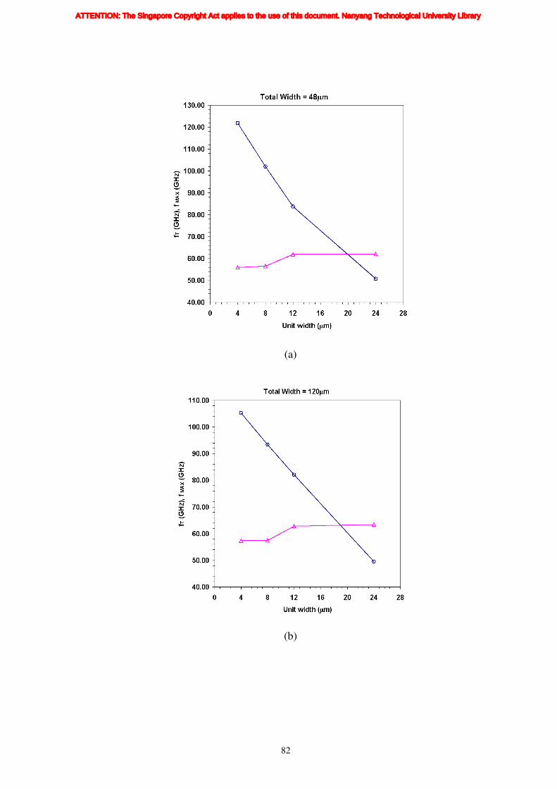
82
(a)
(b)
ATTENTION: The Singapore Copyright Act applies to the use of this document. Nanyang Technological University Library

83
(c)
Fig. 5.4 Extracted fT and fMAX versus unit width for total width of (a) 48 µµµµm,
(b) 120 µµµµm and (c) 240 µµµµm
(a)
fT
fMAX
Dotted Line : gm
Solid Line : Cg
ATTENTION: The Singapore Copyright Act applies to the use of this document. Nanyang Technological University Library

84
(b)
Fig. 5.5 Extracted (a) maximum gm and Cg, (b) Rg and Cgd versus unit width
for total width of 48, 120 and 240 µµµµm
Fig. 5.4 shows the extracted fT and fMAX values for total width of 48, 120
and 240 µm test structures as shown in Table 5.1. The extraction is performed at
maximum gm biasing condition whereby Vgs=1.05 V and Vds=1.8 V. From the
plots, the extracted fT shows similar trend for all the three total width transistors.
Fig. 5.5 (a) and (b) show the extracted maximum gm and Cg values and the Rg and
Cgd values versus unit width for the three total widths transistors.
It is well known that gm and Cg from (5-1) are directly proportional to the
transistor’s width and hence their ratio will result in fT to be independent of the
transistor’s width. But from Fig. 5.4, it shows that the extracted fT changes with the
transistor’s Wf. For smaller Wf of 4 and 8 µm transistors, their extracted fT is
smaller than the transistors with Wf of 12 and 24 µm. Such behavior of fT versus Wf
is due to the parasitic capacitances that exist in the different Wf layout transistor.
For the same total width, smaller Wf transistors will have more fingers and hence
Dotted Line : Rg
Solid Line : Cgd
ATTENTION: The Singapore Copyright Act applies to the use of this document. Nanyang Technological University Library

85
the amount of overlap extrinsic parasitic capacitances will be larger when compare
to large Wf transistors that have smaller finger number. In Fig. 5.5(a), the overall
gate capacitance Cg which includes all the parasitic overlap capacitances increases
with decreasing Wf for all the three total width transistors. This clearly indicates
that transistor with small Wf will have more fingers and cause higher overlap
parasitic capacitances. As for the extracted gm in Fig. 5.5(a), it increases slightly
with decreasing Wf at constant total width. Due to the self-heating effect, the
increasing trend of gm with decreasing Wf is more obvious in large total width
transistor. This is because large total width transistor with small Wf has higher
number of source and drain diffusions as compared to the same total width
transistor with larger Wf. Hence, with more source and drain diffusions, the drain
current is distributed more evenly. This means that less current will flow through
per diffusion. Thus, the heat generated at each diffusion region and its diffusion
resistance change due to temperature will be smaller. Therefore, transistor with
smaller Wf will have higher gm due to less self-heating. Furthermore, it can be
observed that the changes in the extracted gm for a fixed total width is small, so
only the parasitic overlap capacitances in Cg affect the fT versus Wf plot in Fig. 5.4.
The extrinsic overlap parasitic capacitances for Cgs, Cgb and Cgd are shown in Fig.
5.1. Therefore, to optimize Wf based on fT, the width per finger cannot be chosen to
be too small. It is observed from Fig. 5.4 that fT optimization for Wf happens at
about 12 µm for all the three sets of total width transistors. Hence, by increasing
Wf above 12 µm will not improve the fT of the transistor significantly.
From (5-4), it can be deduced that fMAX can be lower or higher than fT based
on the layout of the transistor. In Fig. 5.4, for the three total widths, the extracted
fMAX is observed to be increasing with decreasing Wf. This behavior of fMAX is
ATTENTION: The Singapore Copyright Act applies to the use of this document. Nanyang Technological University Library

86
mainly caused by the change in Rg, fT and Cgd with respect to the change in Wf. For
the same total width with Wf decreasing, the finger number of the transistor
increases and since Rg is proportional to (Wf/Nf), Rg will decrease and cause fMAX to
increase. At the same time, when the finger number increases, the overlap parasitic
capacitances (gate-to-drain, gate-to-source and gate-to-body) will increase and
from (5-1) and (5-2), the transistor’s fT will drop and Cgd (intrinsic and extrinsic
capacitances) will increase and from (5-4), these two parameters will cause fMAX to
decrease. Hence, based on the above analysis, depending on the transistors’ total
width and Wf, certain parasitic effects (Rg and extrinsic overlap capacitances) will
be more dominant than the other, hence influencing the final fMAX trend when Wf
and total width change. Fig. 5.5(b) shows the trend of Rg and Cgd versus unit width
for three total widths. In Fig. 5.4(a) and (b), the trend of fMAX versus Wf is
dominated mainly by the effect from Rg while for Fig. 5.4(c), the extrinsic overlap
parasitic capacitances dominant over Rg causes the trend of fMAX versus Wf to
change. In addition to that, the extracted fMAX value decreases with increasing total
width size for the same Wf; this can be explained by the increase in the overlap
parasitic capacitances in Cg and Cgd as shown in Fig. 5.5(a) and (b) for larger total
width size transistor that has a larger finger number at a fixed Wf. Therefore, based
on Fig. 5.4, it is observed that to optimize the transistor layout using fMAX, the
transistor’s Wf should be chosen to be small.
This study of the Wf effect on fT and fMAX is important and it shows that a
wrong selection of the Wf for transistor layout will cause either fT or fMAX to suffer.
Since the trend of fT and fMAX versus Wf is different, some trade-off is needed when
selecting the best Wf value for transistor to be used in a specific application.
Although both fT and fMAX are commonly used to compare the performance of the
ATTENTION: The Singapore Copyright Act applies to the use of this document. Nanyang Technological University Library

87
transistor but in circuit design such as VCO and transistor gain stages, the power
amplification capability is of more important and hence the fMAX optimization for
the transistor Wf will be very crucial in these applications.
5.4 Unit Width Optimization on High Frequency Noise
The HF noise measurements are performed on-wafer using ATN NP5
Microwave Noise Parameter System. All the three sets of total width transistors are
measured at the maximum gm condition and the frequency range is from 2 to 26.5
GHz. All the measured noise parameters are de-embedded with their
corresponding OPEN structures using the de-embedding feature in the NP5
system. This embedding procedure can be found in [77], whereby the pad and
interconnect parasitic capacitances are de-embedded.
5.4.1 HF noise definition and theory
From the classical RF noise model from Van Der Ziel [54], [55], the high
frequency noise of a transistor can be described by two correlated current noise
sources, the drain noise current (ind) and the induced gate noise current (ing). The
induced gate noise is caused by the capacitive coupling from the channel noise
current. The mean-square representation for drain current noise and gate noise are
shown in (5-7) and (5-8) respectively. Note that c is the correlation factor between
the drain and gate noise sources.
fgkTi dnd ∆= 02 4 γ (5-7)
fg
CkTi
d
gsng ∆
=
0
222
54
ωδ (5-8)
22
ndng
ndng
ii
iic
⋅
⋅≡
∗
(5-9)
ATTENTION: The Singapore Copyright Act applies to the use of this document. Nanyang Technological University Library

88
In (5-7), the parameter gd0 is the drain-source conductance at zero VDS and γ
is the noise factor and has a value of unity at zero VDS and, in long channel devices,
it decreases to a value of 2/3 in saturation region. Note that for short channel
devices operating in saturation region, γ can be considerably higher than the long
channel value. In (5-8), the parameter δ is the gate noise coefficient and it is given
a value of 4/3 in [54].
In [56], [57], the approximated expression for minimum noise factor (Fmin)
is derived as shown in (5-10). In the next section, we will relate this expression to
our measured NFmin. Noted that NFmin is equivalent to Fmin in decibel (dB).
( )isgm
c
MAX
MAX
RRRgf
fRPCRP
f
f
F
++
+⋅−++≈
2
min
2121 (5-10)
fkTg
iP
m
nd
∆=
4
2
(5-11)
fg
CkT
iR
m
gs
ng
∆
=
22
2
4ω
(5-12)
⋅
⋅=
∗
22
Im
ndng
ndng
ii
iiC (5-13)
gs
mc
C
gf
⋅⋅=
π2 (5-14)
The P, R and C noise parameters used in (5-10) are related to the drain and
gate noise current sources as shown in (5-11)-(5-13).
ATTENTION: The Singapore Copyright Act applies to the use of this document. Nanyang Technological University Library
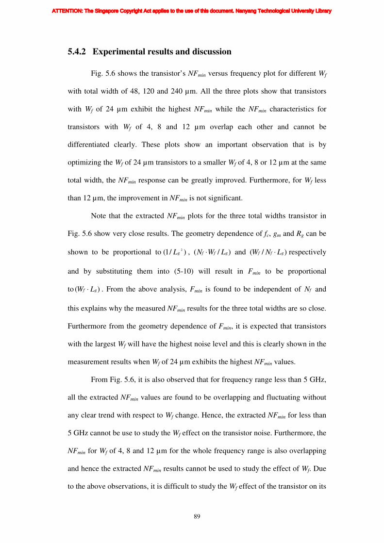
89
5.4.2 Experimental results and discussion
Fig. 5.6 shows the transistor’s NFmin versus frequency plot for different Wf
with total width of 48, 120 and 240 µm. All the three plots show that transistors
with Wf of 24 µm exhibit the highest NFmin while the NFmin characteristics for
transistors with Wf of 4, 8 and 12 µm overlap each other and cannot be
differentiated clearly. These plots show an important observation that is by
optimizing the Wf of 24 µm transistors to a smaller Wf of 4, 8 or 12 µm at the same
total width, the NFmin response can be greatly improved. Furthermore, for Wf less
than 12 µm, the improvement in NFmin is not significant.
Note that the extracted NFmin plots for the three total widths transistor in
Fig. 5.6 show very close results. The geometry dependence of fc, gm and Rg can be
shown to be proportional to )/1( 2gL , )/( gff LWN ⋅ and )/( gff LNW ⋅ respectively
and by substituting them into (5-10) will result in Fmin to be proportional
to )( gf LW ⋅ . From the above analysis, Fmin is found to be independent of fN and
this explains why the measured NFmin results for the three total widths are so close.
Furthermore from the geometry dependence of Fmin, it is expected that transistors
with the largest Wf will have the highest noise level and this is clearly shown in the
measurement results when Wf of 24 µm exhibits the highest NFmin values.
From Fig. 5.6, it is also observed that for frequency range less than 5 GHz,
all the extracted NFmin values are found to be overlapping and fluctuating without
any clear trend with respect to Wf change. Hence, the extracted NFmin for less than
5 GHz cannot be use to study the Wf effect on the transistor noise. Furthermore, the
NFmin for Wf of 4, 8 and 12 µm for the whole frequency range is also overlapping
and hence the extracted NFmin results cannot be used to study the effect of Wf. Due
to the above observations, it is difficult to study the Wf effect of the transistor on its
ATTENTION: The Singapore Copyright Act applies to the use of this document. Nanyang Technological University Library

90
HF noise performance and hence there is a need to propose a new FOM to assist in
this study for the Wf optimization.
(a)
(b)
ATTENTION: The Singapore Copyright Act applies to the use of this document. Nanyang Technological University Library
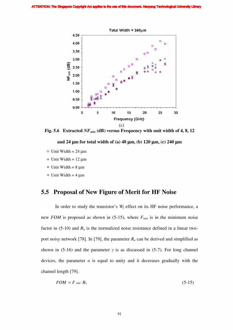
91
(c)
Fig. 5.6 Extracted NFmin (dB) versus Frequency with unit width of 4, 8, 12
and 24 µµµµm for total width of (a) 48 µµµµm, (b) 120 µµµµm, (c) 240 µµµµm
5.5 Proposal of New Figure of Merit for HF Noise
In order to study the transistor’s Wf effect on its HF noise performance, a
new FOM is proposed as shown in (5-15), where Fmin is in the minimum noise
factor in (5-10) and Rn is the normalized noise resistance defined in a linear two-
port noisy network [78]. In [79], the parameter Rn can be derived and simplified as
shown in (5-16) and the parameter γ is as discussed in (5-7). For long channel
devices, the parameter α is equal to unity and it decreases gradually with the
channel length [79].
nRFFOM ⋅= min (5-15)
Unit Width = 24 µm
Unit Width = 12 µm
Unit Width = 8 µm
Unit Width = 4 µm
ATTENTION: The Singapore Copyright Act applies to the use of this document. Nanyang Technological University Library

92
mm
dn
gg
gR
12
0⋅==
α
γγ (5-16)
0d
m
g
g=α (5-17)
By multiplying parameters Fmin and Rn together, the resultant equation is as
shown in (5-18).
4444444444444 34444444444444 21
43421
2
16
1
1
2
3
2
1
term
RRRCCCRg
Kf
term
gFOM
isggsggdg
m
m
+++⋅⋅⋅+
⋅=
π
α
γ
α
γ
(5-18)
RPCRPK 21 −+= (5-19)
By extracting the small signal parameters for all the devices under
comparison and substituting them back into (5-18), the calculated FOM can be
obtained. Fig. 5.7 shows the measured and calculated FOM Fmin·Rn versus
frequency for different Wf transistors at constant total width of 48, 120 and 240
µm. There are three important observations from this FOM versus Wf and total
width change. Firstly, its value is found to be increasing with Wf and decreasing
when the transistor’s total width increases. Note that for the noise figure in Fig.
5.6, only the NFmin trend with Wf is observed, there is no change in the NFmin when
the total width changes. The FOM behavior with respect to the total width and Wf
can be explained by studying the geometry dependences of term1 and term2 in (5-
18). By substituting the geometry dependence of all the parameters into (5-18), it is
clear that term1 and term2 are proportional to )/( ffg WNL ⋅ and )/( 2fg NL
respectively. By adding the proportionality of these two terms, the resultant
ATTENTION: The Singapore Copyright Act applies to the use of this document. Nanyang Technological University Library
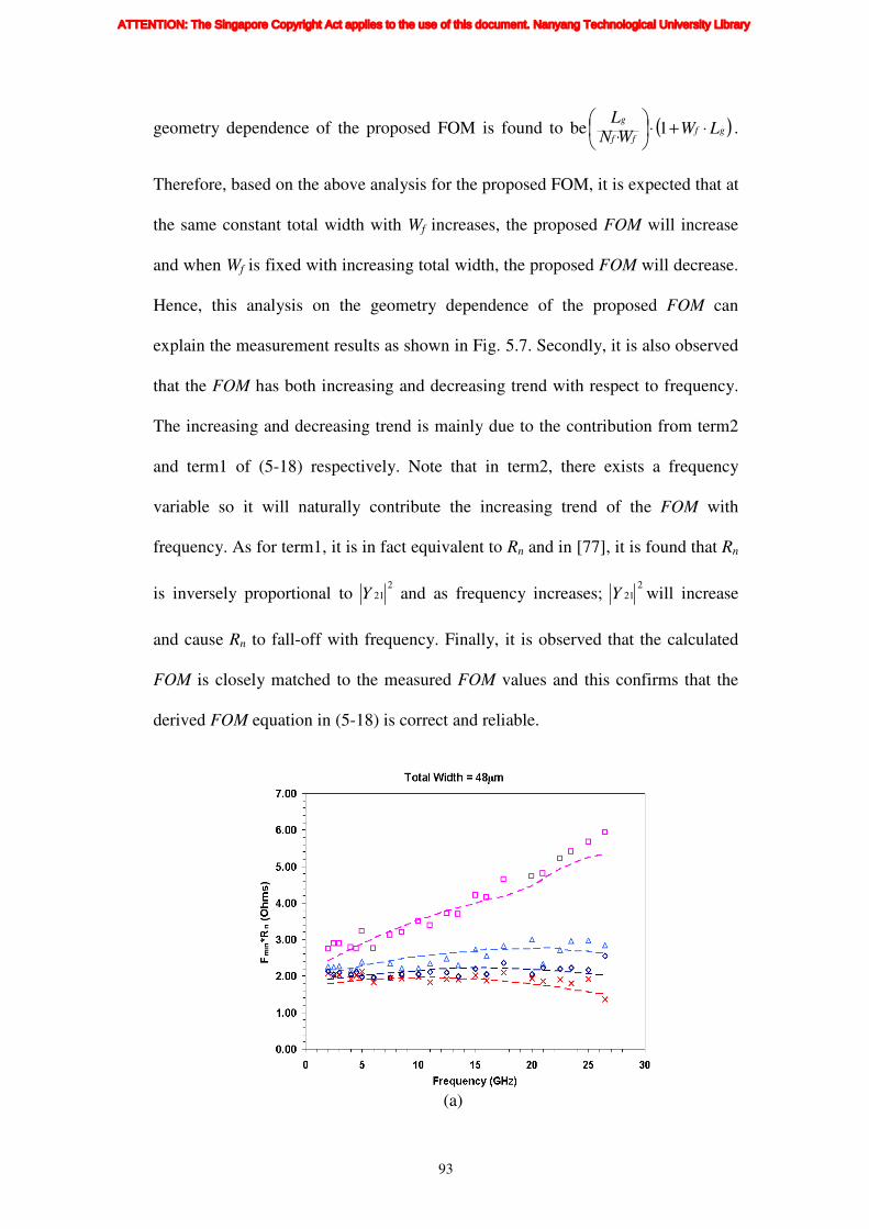
93
geometry dependence of the proposed FOM is found to be ( )gfff
gLW
WNL
⋅+⋅
⋅
1 .
Therefore, based on the above analysis for the proposed FOM, it is expected that at
the same constant total width with Wf increases, the proposed FOM will increase
and when Wf is fixed with increasing total width, the proposed FOM will decrease.
Hence, this analysis on the geometry dependence of the proposed FOM can
explain the measurement results as shown in Fig. 5.7. Secondly, it is also observed
that the FOM has both increasing and decreasing trend with respect to frequency.
The increasing and decreasing trend is mainly due to the contribution from term2
and term1 of (5-18) respectively. Note that in term2, there exists a frequency
variable so it will naturally contribute the increasing trend of the FOM with
frequency. As for term1, it is in fact equivalent to Rn and in [77], it is found that Rn
is inversely proportional to 2
21Y and as frequency increases; 2
21Y will increase
and cause Rn to fall-off with frequency. Finally, it is observed that the calculated
FOM is closely matched to the measured FOM values and this confirms that the
derived FOM equation in (5-18) is correct and reliable.
(a)
ATTENTION: The Singapore Copyright Act applies to the use of this document. Nanyang Technological University Library
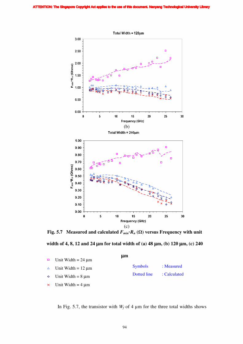
94
(b)
(c)
Fig. 5.7 Measured and calculated Fmin·Rn (Ω) versus Frequency with unit
width of 4, 8, 12 and 24 µµµµm for total width of (a) 48 µµµµm, (b) 120 µµµµm, (c) 240
µµµµm
In Fig. 5.7, the transistor with Wf of 4 µm for the three total widths shows
Symbols : Measured
Dotted line : Calculated
Unit Width = 24 µm
Unit Width = 12 µm
Unit Width = 8 µm
Unit Width = 4 µm
ATTENTION: The Singapore Copyright Act applies to the use of this document. Nanyang Technological University Library

95
the lowest FOM and this implies that it has the lowest noise level when compared
to the noise of the other Wf transistors. Note that such observation is not observable
in Fig. 5.6 as the extracted NFmin for 4, 8 and 12 µm are all overlapping. Therefore,
it is clear that the proposed FOM can help to differentiate the noise level behavior
for different Wf transistor especially for frequency range less than 5 GHz.
Hence, by only considering the HF noise optimization, the transistor’s Wf
should be chosen as 4 µm as they show the lowest noise. Note that the fT of a
transistor with Wf of 4 µm is the lowest while its fMAX is at the highest level. Hence
from Fig. 5.4, if the optimum fT and fMAX performance is required, the Wf should be
chosen at about 12 µm. From Fig. 5.7, the noise for Wf of 12 µm is only slightly
higher and comparable to the 4 µm case. Hence, it can be concluded that for the
optimization of fT, fMAX and HF noise, the optimum Wf to use for a transistor for
this 0.18 µm CMOS technology is at about 12 µm.
5.6 Unit Width Optimization on Flicker Noise
Flicker noise mainly affects the low frequency performance of the
transistor but the impact of flicker noise cannot be neglected in certain RF circuit
such as mixer and VCO because it can up-convert the low frequency noise to high
frequency that can affect the circuit phase noise performance. For example the
phase noise in a VCO will directly affect the adjacent channel rejection and
transmitter signal purity during receiving and transmitting of signals. Furthermore,
it can affect the bit error rate performance of a phased-shift keyed digital
transmission system. Therefore, it is important to study the flicker noise behavior
with respect to the change in Wf of the RF transistor.
Many theories have been presented to explain the flicker noise behavior.
ATTENTION: The Singapore Copyright Act applies to the use of this document. Nanyang Technological University Library

96
The two main theories are the random fluctuation of the carriers in the channel
[40]-[43] and mobility fluctuation [44], [45]. Based on the carrier fluctuation [42],
[43] and mobility fluctuation [44], [45] theories, the noise voltage power spectral
density Svg can be shown as in (5-20) and (5-21) respectively. Note that K1 in (5-
20) is bias independent while in (5-21), K(VGS) is a bias dependent parameter.
Their corresponding noise current power spectral density can be found using (5-
22).
c
gtotalox
vg
fLWC
KS
112
1
⋅= (5-20)
fLWC
VKS
gtotalox
GSvg
11)(
⋅= (5-21)
vgmid SgS ⋅= 2 (5-22)
32
2 1
g
total
gtotalg
totalid
L
W
LWL
WS =
⋅⋅∝ (5-23)
5.6.1 Experimental results and discussion
Fig. 5.8 shows the measured flicker noise versus frequency plot with
varying Wf at fixed total width of 48, 120 and 240 µm. The noise measurement is
done at the maximum gm biasing condition. It is observed that the Wf variation does
not affect the flicker noise performance for the RF transistor for the same total
width condition. Furthermore, the flicker noise current power spectral density Sid is
also found to increase with the total width. In (5-20) or (5-21), it is clear that Svg is
inversely proportional to the total width of the transistor (Wtotal) and while in (5-
22), Sid is directly dependent on the transistor’s gm which is also proportional to
Wtotal. By substituting (5-21) to (5-22), the geometry dependence of Sid can be
ATTENTION: The Singapore Copyright Act applies to the use of this document. Nanyang Technological University Library

97
derived as in (5-23) and it is clearly shown that it is directly dependent on the
transistor’s Wtotal. Therefore, as Wtotal increases, it is expected that Sid to increase
and this is observed in Fig. 5.8. Since the measurement frequency for the flicker
noise is low, the RF parasitic due to the Wf changes will not appear to affect the
transistor’s flicker noise behavior. Therefore, it is expected that Sid shows no
dependency with Wf for the same total width condition.
(a)
(b)
ATTENTION: The Singapore Copyright Act applies to the use of this document. Nanyang Technological University Library

98
(c)
Fig. 5.8 Measured Flicker Noise Sid (A2/Hz) versus Frequency with unit
width of 4, 8, 12 and 24 µµµµm for total width of (a) 48 µµµµm, (b) 120 µµµµm and (c)
240 µµµµm
5.7 Circuit Application Discussion
From the analysis of fT, fMAX, NFmin, the proposed FOM Fmin·Rn and flicker
noise spectral density, the unit width optimization technique can assist designers to
select the optimized layout transistors for a specific circuit application such as
LNA, VCO or mixer that required either low NFmin, high fT or fMAX.
5.7.1 Transistor selection for LNA design
The LNA is usually the first stage of a receiver and it generally requires
low noise figure and high gain transistors in its circuit design. Based on Friss
equation [80], the first stage of the receiver will determine the whole receiver noise
performance; hence the noise in the LNA must be minimized. The transistor size
used for this LNA design is usually large so as to provide enough gain to reduce
the noise in the subsequent stages. The number of fingers for the chosen transistor
ATTENTION: The Singapore Copyright Act applies to the use of this document. Nanyang Technological University Library

99
must be large, hence minimizes its gate resistance. This will cause the amplified
gate noise at the output of the LNA to be small. Therefore, the transistor’s Wf to
use for LNA design should be small so that maximum number of finger can be
achieved for a constant total width transistor. This conclusion coincides with the
analysis that is conducted in section 5.4.
5.7.2 Transistor selection for VCO design
For VCO design, the main considerations are low phase noise and low
power. Since the transistor’s flicker noise will contribute to the output phase noise,
the selected transistor in the VCO design should have low flicker noise spectral
density. From Fig. 5.8, it can be observed that the flicker noise is directly
dependent on the device size and drain current and it is independent of the
transistor’s Wf. Therefore, small total width transistor size with small Wf should be
chosen for the VCO design so that it exhibits low flicker noise spectral density and
high fMAX as presented in Fig. 5.8 and Fig. 5.4 respectively. Furthermore, using
small total width for the transistor also ensure low power consumption for the
VCO.
5.7.3 Transistor selection for Mixer design
The mixer is mainly used in RF transceiver for up and down conversion of
signals. In mixer design, the trade-off for conversion gain, linearity, power
consumption and noise figure have to be studied so as to achieve the design
specifications for the circuit. The noise figure for the mixer is generally large due
to the switching term during the up and down conversion. By designing a mixer
with low noise figure, the gain of the LNA can be low. Hence, from Fig. 5.7,
ATTENTION: The Singapore Copyright Act applies to the use of this document. Nanyang Technological University Library
100
transistor with small Wf can provide the lowest noise level and highest fMAX, which
allows higher operating frequency range for the mixer.
5.8 Summary
In this chapter, the trend of extracted fT and fMAX versus Wf is studied and
from the measurement results, it is clear that for the optimization of both FOMs,
some trade-offs are required. As the measured NFmin for Wf of 4, 8 and 12 µm
cannot reveal their noise behaviors with respect to Wf, a new FOM Fmin·Rn is
proposed. From the calculated Fmin·Rn, it clearly shows that it can be used to
optimize the transistor noise when selecting the best Wf value to be used in low
noise applications. The flicker noise spectral density with varying Wf shows no
optimization can be done for Wf as at such low frequency range, the RF parasitic
will not appear and affect the transistor’s flicker noise. This experiment has shown
that the optimization technique is feasible and can be used to help designers to
select the optimized layout transistors that are optimized specifically for certain
applications such as LNA, VCO and mixer that have low NFmin, high fT or fMAX
requirements. Furthermore, by applying this optimization technique to existing and
future technologies, modeling engineers from foundry and IDM can understand the
RF characteristics of the process and select to model only a small range of
optimized Wf transistors which will shorten the model development time.
ATTENTION: The Singapore Copyright Act applies to the use of this document. Nanyang Technological University Library

101
Chapter 6
SIMPLE AND ACCURATE EXTRACTION
METHODOLOGY FOR RF MOSFET VALID UP
TO 20 GHZ
6.1 Introduction
The fast growth of RF wireless communication market has lead to the
shortening of design cycle time for RF circuits. Therefore, the time required for
developing a RF model and the accuracy of its parameter extraction technique
become very important as the development time will directly impact the time to
market of these RF chips. Hence in this chapter, a simple and accurate parameter
extraction methodology is proposed and demonstrated to be accurate up to 20
GHz.
Up to today, the more commonly used method is by macro modeling
approach. In this approach, sub-circuits are added to the BSIM core model to
model the RF parasitic components of the MOSFET [9], [81]. The sub-circuit
components are usually extracted from the measured S-parameters of the transistor
using Z or Y parameters analysis on the proposed small-signal equivalent circuit
[25], [26], [29], [82].
Presently, there are many different extraction techniques reported [25],
[26], [29], [82] for RF MOSFET modeling. In [82], no substrate resistances are
included in the small-signal equivalent circuit. Thus fitting of the output
admittance will be difficult. The method in [25] requires S-parameter measurement
ATTENTION: The Singapore Copyright Act applies to the use of this document. Nanyang Technological University Library
102
up to about 40 GHz. High frequency measurement of the S-parameter is very
difficult to achieve and it requires very good calibration of equipment and
measurement of de-embedding structures. Furthermore, there is no substrate
network in its equivalent circuit. The approach in [26] is by direct extraction on its
equivalent circuit using Y-parameters analysis in the linear and saturation region.
Its substrate-coupling network is obtained by local optimization to fit the
equivalent substrate admittance. Therefore, no analytical equations are derived for
the substrate-related components. In [29], all the parameters are extracted using a
linear regression approach by performing Y-parameters analysis on the small-
signal equivalent circuit. In this technique, the source and drain resistances are
omitted in the equivalent circuit for simplicity and ease of parameter extraction. As
a result the accuracy of the extracted values for the gate resistance Rg and the
transconductance are compromised. Furthermore, without the source and drain
resistances, the small-signal model gives inaccuracy in noise simulations.
To circumvent the above-mentioned problems from the existing extraction
techniques [25], [26], [29], [82], a new RF parameter extraction technique using
the small-signal equivalent circuit in Fig. 6.1 is presented. It includes three
terminal resistances for the gate, source and drain, a substrate network to
characterize the substrate effect at high frequency and a transcapacitance to ensure
that the small-signal model maintains charge conservation [83]. The RF macro
model for a 0.18 µm 5-finger NMOS transistor is developed using this extraction
technique and good fitting is observed between the measured and simulated results
for frequency up to 20 GHz. The extracted and optimized RF parameter values are
close, which implies that this method is reliable and accurate. The procedure for
the extraction is simple and fast and can be implemented easily for RF MOSFET
ATTENTION: The Singapore Copyright Act applies to the use of this document. Nanyang Technological University Library

103
modeling. The RF macro model includes a BSIM4 model with all its internal
terminal resistances, substrate resistances and capacitance-related parameters
deactivated. The extrinsic components are added to model the parasitic effect at
high frequency during the simulation.
6.2 Measurement Setup
The device under test (DUT) was an NMOS transistor with a channel width
per finger W = 8 µm, a channel length L = 0.18 µm and the number of finger NF =
5. It was fabricated using Chartered Semiconductor Manufacturing Ltd’s 0.18 µm
CMOS Analog/RF technology process. S-parameters were measured using the
HP8510 network analyzer and GSG RF probes for a frequency range from 50 MHz
to 20 GHz. The system calibration was performed first so as to get the cal-set for
the network analyzer and LRRM method was used for the calibration. After the
measurement system was calibrated, the RF transistor and its de-embedding
structures were measured. In this measurement, OPEN and SHORT de-embedding
structures were used to remove the pad and interconnect parasitic.
6.3 Model
Fig. 6.1 New small-signal RF equivalent circuit
gmVgs
Csd
Rg
gds
Cgd
Cgs
Rsubd
D
Cjd
Rd
Rs
dt
dVm
gsC
S
G
gddgm CCC −=
ATTENTION: The Singapore Copyright Act applies to the use of this document. Nanyang Technological University Library

104
Fig. 6.1 shows the proposed new small-signal equivalent circuit. All the
components are physically based and a new approach will be introduced to extract
all the RF parameters. The intrinsic source and substrate are assumed to be shorted
and hence, this model is suitable for transistor that has the source and body
terminal tied together.
The resistance Rg represents the effective lumped gate resistance that
consists of both the electrode resistance and the distributed channel resistance [59].
It has been reported that a simple gate resistance model has been found accurate up
to ½ of fT [31]. The resistances Rs and Rd represent the effective source and drain
resistances that consist of the via, salicide, contact and LDD resistances [84].
The capacitances Cgs and Cgd represent the effective gate-to-source and
gate-to-drain capacitances and consist of both the intrinsic and overlap capacitance
of the transistor. Csd represents the source-to-drain capacitance. Cgd and Cdg
represent the two non-reciprocal capacitances caused by the drain and gate biasing
respectively. Cgd is the capacitance effect on the gate due to the drain while Cdg is
the capacitance effect on the drain due to the gate terminal. Cm represents the
transcapacitance that takes care of the different effects of the gate and the drain on
each other in terms of charging currents [29]. It has also been reported that the
transcapacitance ensures charge conservation [83] in the model and helps to model
the Y12 and Y21 parameter more accurately [29]. The parameters gm and gds
represent the transconductance and the output conductance of the transistor
respectively. The parameters Cjd and Rsubd represent the drain junction capacitance
and the drain-to-substrate resistance respectively. They contribute greatly for the
ATTENTION: The Singapore Copyright Act applies to the use of this document. Nanyang Technological University Library

105
output admittance Y22. Note that Cjd consists of both the junction capacitance and
the intrinsic drain-to-body capacitance.
6.3.1 Extraction of terminal resistances Rg, Rd and Rs
The extraction of the terminal resistances is done by performing Z-
parameter analysis on the equivalent circuit at the linear region of the transistor. It
is proposed that the extraction of the resistances be done at Vgs = 1.8 V and Vds = 0
V. At this biasing condition, the transconductance and transcapacitance are both
close to zero. Since Vds is grounded, there is no drain current and therefore, the
output conductance gds and the capacitance Csd can be neglected. In addition, there
is no voltage drop across Rd and Rs. Therefore, the potential of the intrinsic drain
and source node is the same and Cjd and Rsubd can be removed from the equivalent
circuit. Thus the equivalent circuit can be simplified as shown in Fig. 6.2.
Fig. 6.2 Simplified small-signal equivalent circuit at Vgs = 1.8 V and Vds = 0 V
By applying Z-parameter analysis on the above circuit, the following
equations are obtained.
gs
sg
CjRRZ
ω
111 ++= (6-1)
Rg Rd
S
Cgd
Cgs
D G
Rs
ATTENTION: The Singapore Copyright Act applies to the use of this document. Nanyang Technological University Library
106
gdgs
sd
CjCjRRZ
ωω
1122 +++= (6-2)
gs
s
CjRZZ
ω
12112 +== (6-3)
Note that at this biasing condition the capacitances Cgs and Cgd are equal.
From the above Z-parameter equations, the terminal resistances and the gate-to-
source and gate-to-drain capacitances are extracted using equations (6-4)-(6-7).
( )12ZrealRs = (6-4)
( )1211 ZZrealRg −= (6-5)
( )1222 ZZrealRd −= (6-6)
( )12ZimagCC gdgs == (6-7)
Although parameters Cgs and Cgd can be solved using equation (6-7), they
are not used in the RF model because RF transistors do not operate at this biasing
condition.
6.3.2 Extraction of intrinsic parasitic components
The extracted gate resistance in equation (6-5) is then de-embedded from
the Z-parameters measured at the desired operating biasing condition of the
transistor. It has been reported that poles due to the terminal source and drain
resistances are at a much higher frequency than the typical transit frequency [27].
Therefore, they can be neglected when calculating the Y-parameters of the
equivalent circuit. With the three terminal resistance removed, the equivalent
circuit can be simplified as shown in Fig. 6.3.
ATTENTION: The Singapore Copyright Act applies to the use of this document. Nanyang Technological University Library

107
Fig. 6.3 Simplified small-signal equivalent circuit at Vgs = Vds = 1.2 V
(saturation region)
By performing Y-parameters analysis on the circuit in Fig. 6.3, the
following Y-parameter equations are obtained.
)(11 gdgs CCjY += ω (6-8)
gdCjY ω−=12 (6-9)
dgm CjgY ω−=21 (6-10)
222222
22
22
11 jdsubd
jddsgd
jdsubd
subdjdds
CR
CjCjCj
CR
RCgY
ω
ωωω
ω
ω
++++
++= (6-11)
From the above Y-parameter equations, the rest of the RF parasitic
parameters are obtained using equations (6-12)-(6-16).
( )0
21=
=ω
Yrealgm (6-12)
( )0
22 2 ==
ωYrealgds (6-13)
( )
ω
12YimagCgd −= (6-14)
( ) ( )
ω
1211 YimagYimagCgs
+= (6-15)
gmVgs
Csd gds
Cgd
Cgs
Rsubd
D G
Cjd
dt
dVm
gsC
S
ATTENTION: The Singapore Copyright Act applies to the use of this document. Nanyang Technological University Library

108
( )
ω
21YimagCdg −= (6-16)
For the extraction of the substrate components, Rsubd and Cjd, Ysub is defined
as follows:
222222
22
22
11 jdsubd
jd
jdsubd
subdjd
gdsddssub
CR
Cj
CR
RC
CjCjgYY
ω
ω
ω
ω
ωω
++
+=
−−−=
(6-17)
By plotting ω2/real (Ysub) versus ω2
, the substrate resistance Rsubd can be
obtained from the slope of the plot.
2
22 1
)( jdsubd
subd
sub CRR
Yreal+= ω
ω (6-18)
The drain junction capacitance Cjd is obtained as follows:
2/1
222
)(
−
−= subd
sub
subdjd R
Yreal
RC ω
ω (6-19)
The source-to-drain capacitance Csd is obtained as follows:
( )
222
22
1 jdsubd
jdgdsd
CR
CC
YimagC
ωω +−−= (6-20)
6.4 Extraction and Simulation Results
The extraction of the transconductance gm and output conductance gds at Vgs
= Vds =1.2 V is shown in Fig. 6.4. The parameters gm and gds are obtained from the
Y-intercept as shown in the plot and the extracted values are 19.83 mS and 1.58
mS respectively.
ATTENTION: The Singapore Copyright Act applies to the use of this document. Nanyang Technological University Library
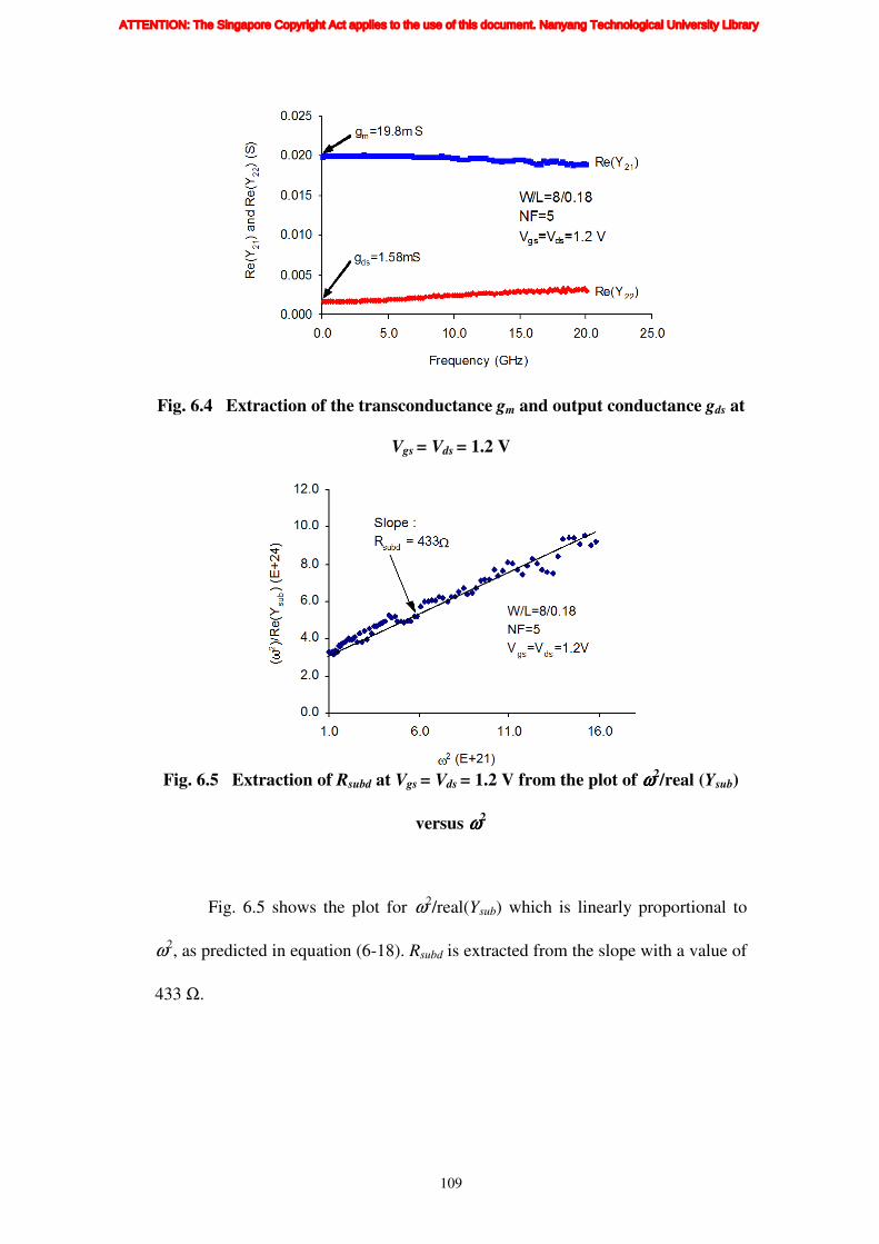
109
Fig. 6.4 Extraction of the transconductance gm and output conductance gds at
Vgs = Vds = 1.2 V
Fig. 6.5 Extraction of Rsubd at Vgs = Vds = 1.2 V from the plot of ωωωω2
/real (Ysub)
versus ωωωω2
Fig. 6.5 shows the plot for ω2/real(Ysub) which is linearly proportional to
ω2, as predicted in equation (6-18). Rsubd is extracted from the slope with a value of
433 Ω.
ATTENTION: The Singapore Copyright Act applies to the use of this document. Nanyang Technological University Library

110
0.0
2.0
4.0
6.0
8.0
10.0
12.0
14.0
16.0
18.0
20.0
3.0 4.0 5.0 6.0 7.0 8.0 9.0 10.0
Frequency (GHz)
Rg, R
d a
nd R
s (
Ohm
s)
Rd
Rs
Rg
W/L=8/0.18
NF=5
Vgs=1.8V
Vds=0V
Rd = 9 .4
Rg = 7 .7
Rs = 9.0
Fig. 6.6 Extraction of Rg, Rd and Rs at Vgs=1.8 V and Vds=0 V
Fig. 6.6 shows the plot for the terminal resistances versus frequency. It is
observed that the terminal resistances are almost frequency independent. From the
plot, the terminal resistances Rg, Rd and Rs are found to be 7.7 Ω, 9.4 Ω and 9.0 Ω
respectively. Note that the extracted source and drain resistance values are about
the same and the small discrepancy of 0.4 Ω could be due to the accuracy of the
measurement tool.
0.0
10.0
20.0
30.0
40.0
50.0
60.0
70.0
80.0
3.0 4.0 5.0 6.0 7.0 8.0 9.0 10.0
Frequency (GHz)
Ca
pa
citan
ce (
fF)
Csd (fF)
Cgs (fF)
Cjd (fF)
Cdg (fF)
Cgd (fF)
W/L=8/0.18
NF=5
Vgs=Vds=1.2V
Fig. 6.7 Frequency plot for Cgs, Cgd, Cdg, Cjd and Csd extracted at Vgs = Vds =
1.2 V
Fig. 6.7 shows the plot for Cgs, Cgd, Cdg, Cjd and Csd extracted at Vds = Vds =
1.2 V. From the plot, these components remain almost constant throughout the
ATTENTION: The Singapore Copyright Act applies to the use of this document. Nanyang Technological University Library

111
frequency range. This implies that the de-embedding of the pad and interconnect
parasitic are done correctly and the extraction routine is robust and reliable. It is
also observed that the Cdg is in fact different from Cgd.
Before simulating for the S-parameters, DC modeling for the transistor
must first be modeled well. This is because the transconductance gm and output
resistance rds at DC condition will affect the S-parameter at low frequency range.
Therefore, if the DC characteristics are not well fitted, it will be very difficult to
achieve good fitting for the S-parameters at low frequency range. Note that the
reciprocal of rds is equivalent to the output conductance gds.
Before the DC I-V curves are fitted with BSIM4 model, the RF parasitic
components must first be extracted and included into the macro model as sub-
circuit components. At DC condition, the current through the gate is very small;
therefore the gate resistance will not affect the I-V curve very much. As for the
source and drain resistances, they must be included into the macro model during
DC modeling of the I-V curves. This is because when the drain current is large, the
potential drop across the source and drain resistances will be large too, therefore
their effective terminal voltages will be reduced. As for all the RF parasitic
capacitors, they will be treated as open-circuit at DC operating condition.
After the DC fitting of the I-V characteristics, transconductance and output
resistance of the 5-finger NMOS transistor, the macro model is then used in the
simulation for its S-parameters. The simulation is done at Vgs = Vds = 1.2 V, which
is the same biasing condition used during the extraction of the RF parasitic
components. Since the extracted component values are obtained mainly by the line
regression method, the values extracted are only estimated. In order to achieve the
ATTENTION: The Singapore Copyright Act applies to the use of this document. Nanyang Technological University Library

112
best fit for the simulated and measured S-parameter data, an optimization for all
the RF component values must be done.
Table 6.1 shows the extracted parameter values and the optimized
parameter values for a 5-finger NMOS transistor with a channel length of 0.18 µm
and a channel width of 8 µm. From Table 6.1, it is observed that the extracted
values are actually quite close to the optimized values. This further shows that the
proposed extraction method is accurate and reliable.
Table 6.1 Extracted and optimized parameter values for a 5-finger NMOS
transistor with L = 0.18 µµµµm and W = 8 µµµµm at Vgs = Vds = 1.2 V
RF
parameters
Extracted
values
Optimized
values
gm, mS 19.83 19.8
gds, mS 1.58 1.53
Cdg, fF 24.3 24.3
Rg, Ω 7.7 8.2
Rd, Ω 9.4 9.4
Rs, Ω 9.0 9.0
Cgs, fF 40 42.77
Cgd, fF 16 16.16
Rsubd, Ω 433 380
Cjd, fF 26.6 28.68
Csd, fF 40 35.93
ATTENTION: The Singapore Copyright Act applies to the use of this document. Nanyang Technological University Library

113
0.00E+00
1.00E-03
2.00E-03
3.00E-03
4.00E-03
5.00E-03
6.00E-03
7.00E-03
0.0 5.0 10.0 15.0 20.0 25.0
Frequency (GHz)
Re(Y
11)
and Im
(Y1
1)
(S)
Im(Y11
)
Re(Y11
)
(a)
-2.50E-03
-2.00E-03
-1.50E-03
-1.00E-03
-5.00E-04
0.00E+00
5.00E-04
0.0 5.0 10.0 15.0 20.0 25.0
Frequency (GHz)
Re(Y
12)
and I
m(Y
12)
(S)
Im(Y12
)
Re(Y12
)
(b)
-1.00E-02
-5.00E-03
0.00E+00
5.00E-03
1.00E-02
1.50E-02
2.00E-02
2.50E-02
0.0 5.0 10.0 15.0 20.0 25.0
Frequency (GHz)
Re(Y
21)
and I
m(Y
21)
(S)
Re(Y21)
Im(Y21)
(c)
ATTENTION: The Singapore Copyright Act applies to the use of this document. Nanyang Technological University Library
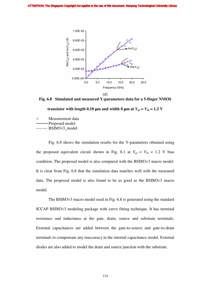
114
0.00E+00
2.00E-03
4.00E-03
6.00E-03
8.00E-03
1.00E-02
0.0 5.0 10.0 15.0 20.0 25.0
Frequency (GHz)
Re(Y
22)
and I
m(Y
22)
(S)
Im(Y22)
Re(Y22)
(d)
Fig. 6.8 Simulated and measured Y-parameters data for a 5-finger NMOS
transistor with length 0.18 µµµµm and width 8 µµµµm at Vgs = Vds = 1.2 V
Measurement data
Proposed model
-------- BSIM3v3_model
Fig. 6.8 shows the simulation results for the Y-parameters obtained using
the proposed equivalent circuit shown in Fig. 6.1 at Vgs = Vds = 1.2 V bias
condition. The proposed model is also compared with the BSIM3v3 macro model.
It is clear from Fig. 6.8 that the simulation data matches well with the measured
data. The proposed model is also found to be as good as the BSIM3v3 macro
model.
The BSIM3v3 macro model used in Fig. 6.8 is generated using the standard
ICCAP BSIM3v3 modeling package with curve fitting technique. It has terminal
resistance and inductance at the gate, drain, source and substrate terminals.
External capacitances are added between the gate-to-source and gate-to-drain
terminals to compensate any inaccuracy in the internal capacitance model. External
diodes are also added to model the drain and source junction with the substrate.
ATTENTION: The Singapore Copyright Act applies to the use of this document. Nanyang Technological University Library

115
0.0
10.0
20.0
30.0
40.0
50.0
60.0
70.0
1.0E+07 1.0E+08 1.0E+09 1.0E+10 1.0E+11
Frequency (Hz)
10*L
OG
10(m
ag(H
21)2
) (d
B)
Fig. 6.9 Simulated and measured results for 10*Log10(mag(H21)2) versus
Frequency in log scale for a 5-finger NMOS transistor with length 0.18 µµµµm
and width 8 µµµµm at Vgs = Vds =1.2 V
Measurement data
Proposed model
Fig. 6.9 shows the simulated and measured results for the magnitude of H21
obtained using the proposed equivalent circuit. The cut-off frequency (fT) can be
extracted from the X-intercept in Fig. 6.9. It is observed that the simulated and the
measured results are in close agreement.
The proposed extraction methodology is also applied to an NMOS
transistor with finger number of 5, channel width per finger of 8 µm and channel
length of 0.25 µm. The gate and drain-bias dependences for the extracted
capacitances and Rsubd are shown in Figs. 6.10 and 6.11 respectively.
ATTENTION: The Singapore Copyright Act applies to the use of this document. Nanyang Technological University Library

116
0
10
20
30
40
50
60
70
0 0.5 1 1.5 2
Vgs (V)
Capacitance (
fF)
Ext_Cgs
Ext_Cdg
Ext_Cgd
Ext_Csd
Ext_Cjd
LinearSaturation
(a)
1.E+02
1.E+03
0 0.5 1 1.5 2
Vgs (V)
Rsub
d (
Ω)
Ext_Rsubd
(b)
Fig. 6.10 Gate bias dependence on the extracted (a) Capacitances and (b)
Rsubd of a 5-finger NMOS transistor with length 0.25 µµµµm and width 8 µµµµm
biased at Vds = 1.2 V
0
10
20
30
40
50
60
70
0 0.5 1 1.5 2
Vds (V)
Ca
pa
cita
nce
(fF
)
SaturationLinear
Ext_Cgs
Ext_Cgd
Ext_Cdg
Ext_CsdExt_Cjd
(a)
ATTENTION: The Singapore Copyright Act applies to the use of this document. Nanyang Technological University Library

117
1.E+02
1.E+03
0 0.5 1 1.5 2
Vds (V)
Rsu
bd (
Ω)
Ext_Rsubd
(b)
Fig. 6.11 Drain bias dependence on the extracted (a) Capacitances and (b)
Rsubd of a 5-finger NMOS transistor with length 0.25 µµµµm and width 8 µµµµm
biased at Vgs = 1.2 V
The capacitances Cgd, Cgs, Cjd and Cdg consist of the intrinsic and overlap
capacitance. The intrinsic capacitance is normally bias dependent while the overlap
capacitance is bias independent. Therefore as seen in Fig. 6.10(a), when Vgs
increases, the channel charges built-up and increases the intrinsic component of the
extracted capacitances. Note that Cgs and Cdg has strong gate-bias dependence
while Cgd only increase slightly with the gate bias. This is because at saturation
condition, Cgd is dominated by the overlap capacitance. Note that Csd is not
affected by the gate bias. From Fig. 6.10(b), it is observed that Rsubd remains
almost constant for Vgs > 0.9 V. Therefore, it is concluded that at strong inversion
region, the extracted parameters are almost constant with gate bias.
From Fig. 6.11(a), it is observed that as Vds increases; there is a small
increase in Cgs. This is because the transistor is approaching the saturation region
and the channel is entering “pinched-off” when Vds reaches Vgs-Vt0. When the
channel is approaching “pinch-off” condition, the channel charge in the source side
ATTENTION: The Singapore Copyright Act applies to the use of this document. Nanyang Technological University Library

118
increases and hence the intrinsic capacitance of Cgs also increases. As for Cgd,
when the channel is approaching “pinch-off” condition, the charge in the intrinsic
drain region decreases causing the intrinsic capacitance Cgd to decrease. The slight
drop in Cjd is due to the increase in the drain junction depletion thickness when Vds
increases. From Figs. 6.11(a) and (b), it is observed that at high Vds bias, the
extracted parameters remain almost constant.
Therefore, from Figs. 6.10 and 6.11, it is concluded that by biasing the
transistor at strong inversion region (Vgs > 0.9 V) and at high Vds bias (Vds > 0.9 V),
the extracted RF parameter values are almost constant and the developed RF
macro model is valid for that range of biasing condition.
6.5 Summary
A novel extraction technique for obtaining the RF parasitic parameters for a
0.18 µm MOSFET is presented. All the RF parameters are extracted analytically
using Z and Y parameter analysis. The technique is simple and straightforward and
can be implemented into a circuit simulation environment very easily. The extracted
and optimized parameter values are in close agreement with the measurement data.
The method is reliable as excellent agreement between the simulated and measured
result is achieved up to 20 GHz. Furthermore, the gate and drain-bias dependences
of the extracted RF parameter values are almost constant for Vgs > 0.9 V and Vds >
0.9 V. Therefore, the RF macro model developed using this technique is valid for
the above range of biasing condition.
ATTENTION: The Singapore Copyright Act applies to the use of this document. Nanyang Technological University Library
119
Chapter 7
SCALABLE RFCMOS TRANSISTOR
MODELING AND ITS VERIFICATION
TECHNIQUE FOR RF CIRCUIT DESIGN
7.1 Introduction
The relentless scaling down of CMOS technologies has greatly improved
the RF performance of MOSFET. It has been reported that for a technology node
of 90 nm, high fT of 209 GHz and fMAX of 248 GHz are achieved [85]. Furthermore,
the scaling down of the transistor has brought about lower NFmin and it is now
comparable to the reported SiGe BJT process [85], [86]. The improved RFCMOS
performance coupled with its lower cost has motivated circuit designers to
integrate digital, mixed-signal and RF transceiver blocks into a single chip [87]-
[91]. However, for these RF chips to operate at higher frequency regions, the
circuit design specifications have to be more stringent and this will require
accurate and scalable RFCMOS model that can be simulated accurately at high
frequency regions. Furthermore, by employing scalable RFCMOS model into the
process design kit (PDK), the circuit design environment is improved and this can
help circuit designers in their circuit optimization to shorten the design cycle and
time to market of these RF chips.
Most of the RF models developed today are based on the macro modeling
approach. In this approach, sub-circuit components are added to the transistor’s
core model to model the RF parasitic of MOSFET structure [9], [81] and the core
ATTENTION: The Singapore Copyright Act applies to the use of this document. Nanyang Technological University Library

120
model used are usually the commercially available models such as BSIM3v3 [92]
and BSIM4 [60]. The sub-circuit components are extracted from the measured S-
parameters of the transistor but the extracted values of these RF components can
be different when different extraction technique is used. All the existing RF
parameter extraction technique is based on the transistor’s small-signal equivalent
circuit analysis. Therefore to characterize a RF MOSFET, all its RF parasitic
elements must be included into the small-signal equivalent circuit. Although it has
been demonstrated that by including the sub-circuit components into the core
model can accurately simulate the transistor’s RF characteristics, such developed
model is normally for discrete transistor sizes. In order to generate a geometry
scalable RFCMOS model, the extracted sub-circuit component values must be
studied for its geometry dependency and by formulating equations to capture their
physical effects at high frequency regions; a physical scalable RFCMOS model
can be generated. Presently, some publications are reported for the scalable RF
MOSFET modeling [93]-[95] but these publications [93], [95] do not show all the
geometry scalable equations of the sub-circuit components. In [94], the formulated
equations for these sub-circuit components were empirical and have no physical
meaning and furthermore, only one device size of fT and fMAX plot are presented.
In this experiment, the geometry dependences of the RF sub-circuit
components are studied and the formulation of these RF components is done based
on their physical effects and the geometry of the layout structure. The scalable
transistor’s RF characteristics with respect to its layout geometry, biasing and
frequency are demonstrated with good accuracy between the measured and
simulated results. Presently, there is no proposed standard technique for
quantifying the quality of a developed scalable RF model. Hence, a new technique
ATTENTION: The Singapore Copyright Act applies to the use of this document. Nanyang Technological University Library
121
is proposed to help modeling engineers to verify and check the developed scalable
RF model for their scalability and accuracy. By utilizing this proposed technique,
the model geometry scalability with respect to the transistor’s unit width (Wf) and
finger number (Nf) are checked to ensure that the formulated geometry equations
are correct. Furthermore, by plotting the proposed accuracy plots, the error
population of the developed model is verified and ensured that they are below the
error’s specification of the developed model. In most RF circuit design, optimal
noise performance is one of the critical specifications that require circuit designers
to fulfill. Hence, it is critical that the developed scalable RF model is able to
predict the noise performance of the transistor accurately. In this chapter, the RF
noise model is developed and simulated to show its accuracy in predicting the
measured noise performance. The scalable RF model was developed for a 90 nm
process with channel length of 70 nm for a frequency range of 50 MHz to 49.85
GHz. The devices under test (DUT) are NMOS transistors with varying Nf of 4, 8,
16, 24, 32, 48 and 64, Wf of 1, 2.5 and 5 µm and at fixed channel length Lg of 70
nm. As RFCMOS technology advances, the requirement for the circuit design’s
operating frequency is getting higher and hence, only short channel length
transistors can achieve the higher operating frequency with the required gain. By
studying the geometry dependence of the RF sub-circuit components for the above
DUTs, the physical geometry equations with fabrication process parameters are
formulated and from the comparison between the extracted and calculated
component values show excellent agreement for all the above combination of Nf
and Wf. Note that the calculated values are computed from the developed scalable
equations formulated for each parasitic component and the extracted values are
ATTENTION: The Singapore Copyright Act applies to the use of this document. Nanyang Technological University Library

122
obtained from the best fitted component values used to minimize the error between
the measured and simulated S-parameters.
7.2 Scalable RF MOSFET Modeling
Fig. 7.1 RF equivalent sub-circuit model
Fig. 7.1 shows the proposed RF equivalent sub-circuit model. All the sub-
circuit components are physically based and can be used for transistor that has the
source and body terminal tied together and grounded.
The resistance Rgate represents the effective lumped gate resistance that
consists of both the electrode resistance and the distributed channel resistance [59].
The resistances Rs and Rd represent the effective source and drain resistance that
consists of the metal line, via and contact resistances.
The capacitance Cgs_ext and Cgd_ext represent the effective gate to source and
gate to drain capacitance and consist of both the overlap and fringing capacitance
ATTENTION: The Singapore Copyright Act applies to the use of this document. Nanyang Technological University Library

123
between the terminals. Cds represents the drain to source fringing capacitance
between the metal lines that connect to the source and drain diffusions. As the
internal junction capacitances of the core model are turned off, the external diodes
Djdb, Djdb_perim, Djsb and Djsb_perim are added as the junction capacitances to connect
the substrate resistance network. Djdb stands for the area intensive diode while the
Djdb_perim stands for the perimeter intensive diode and the definition is the same for
the source to body junction diodes. The parameters Rsub1, Rsub2 and Rsub3 represent
the substrate network resistances. Finally, Csubg and Rsubg are defined as the gate to
substrate capacitance and resistance over the shallow trench isolation (STI) region.
Fig. 7.2 Simplified RF NMOS layout
Fig. 7.2 shows the simplified layout of the RF NMOS transistor. The
transistor has a multi-finger configuration with double contacted gate poly
structure. Dummy gate poly is added to improve the gate structure formation and
metal 1 and 2 are used for the connection of the gate terminal. The source
ATTENTION: The Singapore Copyright Act applies to the use of this document. Nanyang Technological University Library

124
diffusions are connected using the metal 1 layer and shorted to the body terminal
or P-well while the drain diffusions are pulled out using the metal 3 layer.
In order to extract physical sub-circuit components in the macro model, all
the physical layers and their geometries that are used to form the structure of the
transistor must be known. The extraction technique used to extract the sub-circuit
components values is as shown in [34].
7.2.1 Gate resistance modeling
Fig. 7.3 shows the simplified polysilicon gate structure and its distributed
parasitic resistances. At RF frequency region, Rgate is influenced by three physical
effects. The three effects are the distributed gate electrode resistancefWpolygR _, , the
non-quasi-static (NQS) effect in the channel chgR , [59], [96] and the polysilicon
gate extension of the active region extWpolygR _, as shown in (7-1).
Distributed gate electrode
Source Drain
Gate oxide
Distributed Channel
Fig. 7.3 Simplified polysilicon gate structure and its distributed parasitic
resistances
extf WpolygchgWpolyggate RRRR _,,_, ++= (7-1)
ATTENTION: The Singapore Copyright Act applies to the use of this document. Nanyang Technological University Library

125
In [24], the distributed effect of the gate electrode has been studied and the
following equations have been derived to calculate the distributed gate electrode
resistance.
f
gfpoly
WpolygN
LWR
f ⋅=
⋅
3
/_,
ρ, Single contacted gate (7-2)
f
gfpoly
WpolygN
LWR
f ⋅=
⋅
12
/_,
ρ, Double contacted gate (7-3)
In (7-2) and (7-3), the variable Nf is the number of finger, ρpoly is the gate
sheet resistance, and Lg and Wf is the channel length and unit width of a single
finger. The factor of 1/3 and 1/12 are used in (7-2) and (7-3) to account for the
distributed gate resistance effect and the different gate connection configuration at
the ends of the gate structure. As the gate electrode of the DUTs are double
contacted at both ends as shown in Fig. 7.3, the resistance fWpolygR _, in (7-3) is
used in the gate resistance modeling..
The polysilicon gate extension Wext as shown in Fig. 7.3 contribute to the
total gate resistance as shown in (7-4). Note that Wext is divided by 2 in (7-4) as the
polysilicon gate extension regions at both ends are connected in parallel as shown
in Fig. 7.3.
gf
extpoly
WpolygLN
W
Rext ⋅
=
⋅
2_,
ρ (7-4)
At RF frequency region, the channel will behave like a distributed RC
network as shown in Fig. 7.3. The distributed channel resistance will reflect to the
gate through the capacitance network and increases the total gate resistance. Note
that this NQS channel resistance is bias and geometry dependence. However, it is
reported that a simple gate resistance can model the distributed gate resistance
ATTENTION: The Singapore Copyright Act applies to the use of this document. Nanyang Technological University Library
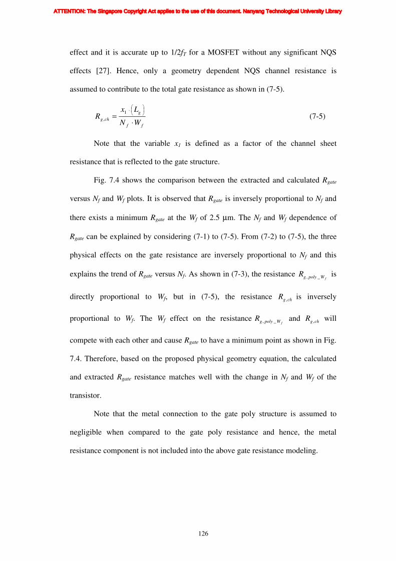
126
effect and it is accurate up to 1/2fT for a MOSFET without any significant NQS
effects [27]. Hence, only a geometry dependent NQS channel resistance is
assumed to contribute to the total gate resistance as shown in (7-5).
ff
g
chgWN
LxR
⋅=
⋅1
, (7-5)
Note that the variable x1 is defined as a factor of the channel sheet
resistance that is reflected to the gate structure.
Fig. 7.4 shows the comparison between the extracted and calculated Rgate
versus Nf and Wf plots. It is observed that Rgate is inversely proportional to Nf and
there exists a minimum Rgate at the Wf of 2.5 µm. The Nf and Wf dependence of
Rgate can be explained by considering (7-1) to (7-5). From (7-2) to (7-5), the three
physical effects on the gate resistance are inversely proportional to Nf and this
explains the trend of Rgate versus Nf. As shown in (7-3), the resistance fWpolygR _, is
directly proportional to Wf, but in (7-5), the resistance chgR , is inversely
proportional to Wf. The Wf effect on the resistancefWpolygR _, and chgR , will
compete with each other and cause Rgate to have a minimum point as shown in Fig.
7.4. Therefore, based on the proposed physical geometry equation, the calculated
and extracted Rgate resistance matches well with the change in Nf and Wf of the
transistor.
Note that the metal connection to the gate poly structure is assumed to
negligible when compared to the gate poly resistance and hence, the metal
resistance component is not included into the above gate resistance modeling.
ATTENTION: The Singapore Copyright Act applies to the use of this document. Nanyang Technological University Library

127
Fig. 7.4 Extracted and calculated Rgate versus (a) Nf and (b) Wf
7.2.2 Source and drain resistance modeling
The resistances Rs and Rd shown in Fig. 7.1 are defined as the effective
resistances that consist of the metal line, via and contact resistances as depicted in
the layout in Fig. 7.5. It is assumed that the source and drain resistances in
BSIM3v3 model only models the active region of the parasitic resistances. Based
on the layout below, the following equations can be derived to represent Rs and Rd.
(a)
(b)
ATTENTION: The Singapore Copyright Act applies to the use of this document. Nanyang Technological University Library

128
Fig. 7.5 Source and drain metal structure
sourcediff
con
conm
sn
n
R
x
l
R,
1
11
+
⋅
=
ρ
(7-6)
draindiff
con
viaviaconm
dn
n
RRR
x
l
R,
21
2
23 )(
+++
⋅
=
ρ
(7-7)
The variables, ρm1 and ρm3, represent the sheet resistances for metal layers 1
and 3; the variables, Rcon, Rvia1 and Rvia2, represent the contact, via1 and via2
resistances; and ncon, ndiff,source and ndiff,drain is the number of contacts, and the source
and drain diffusions in the transistor.
Fig. 7.6 shows the comparison between the extracted and calculated Rs and
Rd versus Nf plots. It is observed that both resistances are inversely proportional to
Nf and there exists a minimum point of resistance value at a Wf of 2.5 µm. From (7-
6) and (7-7), the ndiff,source and ndiff,drain are noted to be proportional to Nf. Hence, Rs
and Rd resistances show the inverse proportionality with Nf. From Fig. 7.5, the
ATTENTION: The Singapore Copyright Act applies to the use of this document. Nanyang Technological University Library

129
variables l1, l2 and ncon are proportional to the Wf of the transistor and when they
are applied to (7-6) and (7-7), the Wf effect on both l1 and l2 will compete with ncon
and caused a minimum resistance level to occur at Wf of 2.5 µm.
Fig. 7.6 Extracted and calculated (a) Rs and (b) Rd versus Nf
7.2.3 Gate to substrate capacitance and resistance modeling
The components Csubg and Rsubg that are shown in Fig. 7.1 are defined as the
gate to substrate capacitance and resistance over the STI region, respectively, and
they are shown in the cross sectional structure in Fig. 7.7. The dotted enclose
region in Fig. 7.7 are the gate area that is on top of the STI region generating the
(a)
(b)
ATTENTION: The Singapore Copyright Act applies to the use of this document. Nanyang Technological University Library

130
parasitic components Csubg and Rsubg and based on the layout geometry, the
following equations are formulated.
2,21,1 MSTIMMSTIMsubg aCaCC ⋅+⋅= (7-8)
The variables, STIMC ,1 and STIMC ,2 , are the parasitic capacitances per unit
area of metals 1 and 2 over the STI region, while the variable 1Ma and 2Ma are the
area of the dotted enclosed region of metals 1 and metal 2 as shown in Fig. 7.7.
f
STIsubstrate
subgN
RR
,= (7-9)
Fig. 7.7 Gate to substrate capacitance and resistance structure
ATTENTION: The Singapore Copyright Act applies to the use of this document. Nanyang Technological University Library
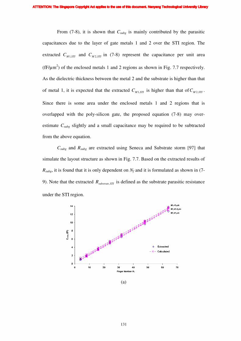
131
From (7-8), it is shown that Csubg is mainly contributed by the parasitic
capacitances due to the layer of gate metals 1 and 2 over the STI region. The
extracted STIMC ,1 and STIMC ,2 in (7-8) represent the capacitance per unit area
(fF/µm2) of the enclosed metals 1 and 2 regions as shown in Fig. 7.7 respectively.
As the dielectric thickness between the metal 2 and the substrate is higher than that
of metal 1, it is expected that the extracted STIMC ,1 is higher than that of STIMC ,2 .
Since there is some area under the enclosed metals 1 and 2 regions that is
overlapped with the poly-silicon gate, the proposed equation (7-8) may over-
estimate Csubg slightly and a small capacitance may be required to be subtracted
from the above equation.
Csubg and Rsubg are extracted using Seneca and Substrate storm [97] that
simulate the layout structure as shown in Fig. 7.7. Based on the extracted results of
Rsubg, it is found that it is only dependent on Nf and it is formulated as shown in (7-
9). Note that the extracted STIsubstrateR , is defined as the substrate parasitic resistance
under the STI region.
(a)
ATTENTION: The Singapore Copyright Act applies to the use of this document. Nanyang Technological University Library

132
(b)
Fig. 7.8 Extracted and calculated (a) Csubg and (b) Rsubg versus Nf
Fig. 7.8 shows the comparison between the extracted and calculated Csubg
and Rsubg versus Nf plots. It is observed that Csubg is proportional to Nf while Rsubg is
inversely proportional to Nf. In (7-8), Csubg is dependent on 1Ma and 2Ma . When Nf
increases, these two areas will increase and cause Csubg to increase.
Based on the layout structure in Fig. 7.7, it is observed the length of lx is
proportional to Nf. By using the simple resistance equation, which is the multiple
of the sheet resistance and the number of squares, it is obvious that the number of
squares in the signal flow path of Rsubg is inversely proportional to the length of lx.
Hence, Rsubg will decrease with increasing Nf.
Note that the metals 1 and 2 regions as shown in Fig. 7.7 should generate a
resistor at the input of the gate poly structure. But it is assumed that the metal
resistances are usually negligible when compared to the gate poly resistance and
hence, it is omitted in the Section 7.2.1 of the gate resistance modeling.
ATTENTION: The Singapore Copyright Act applies to the use of this document. Nanyang Technological University Library

133
7.2.4 Gate to source and gate to drain capacitance modeling
The capacitances Cgs_ext and Cgd_ext in Fig. 7.1 represent the overlap and
fringing capacitances between the gate to source and gate to drain terminals as
shown in Fig. 7.9. Based on the above layout structure, it is obvious that the
amount of overlap capacitance is dependent on the number of source and drain
metal lines that overlaps the gate metal while the fringing capacitances depend on
the separation distance between the source/drain metal lines to gate poly-silicon
structure and the Wf of the transistor. Since the separation distance between the
source/drain metals lines to the gate poly-silicon structure is fixed, therefore the
fringing capacitance is only dependent on transistor’s Wf. Based on the above
analysis, the following equations are formulated.
fffringinggsPolyMsourcediffoverlapgsMMextgs WNCnCC ⋅⋅+⋅= −− _,1,_,12_ (7-10)
Note that overlapgsMMC _,12− is the overlap capacitance (fF) between the gate
(metal 2) and source (metal 1) metal lines and fringinggsPolyMC _,1− is the fringing
capacitance per unit width (fF/µm) between the gate structure (poly-silicon) and
the source (metal 1) metal lines.
fffringinggdPolyMdraindiffoverlapgdMMextgd WNCnCC ⋅⋅+⋅= −− _,1,_,13_ (7-11)
Note that overlapgdMMC _,13− is the overlap capacitance (fF) between the gate
(metal 1) and drain (metal 3) metal lines and fringinggdPolyMC _,1− is the fringing
capacitance per unit width (fF/µm) between the gate structure (poly-silicon) and
the drain (metal 1) metal lines. It is assumed that the fringing capacitances from
the metal 2 and metal 3 lines of the drain metal structure to the poly-silicon gate is
ATTENTION: The Singapore Copyright Act applies to the use of this document. Nanyang Technological University Library

134
small and negligible when compare to the metal 1 to the poly-silicon gate fringing
capacitance.
Fig. 7.9 Gate to source and gate to drain capacitance structure
As the dielectric separation between the metal 3 (drain) and metal 1 (gate)
is larger than the case of metal 2 (gate) and metal 1 (source), it is expected that
overlapgsMMC _,12− to be larger than overlapgdMMC _,13− . Furthermore, the extracted
fringinggsPolyMC _,1− must be close to the extracted fringinggdPolyMC _,1− or slightly smaller.
ATTENTION: The Singapore Copyright Act applies to the use of this document. Nanyang Technological University Library

135
Fig. 7.10 Extracted and calculated (a) Cgs_ext and (b) Cgd_ext versus Nf
Fig. 7.10 shows the comparison between the extracted and calculated Cgs_ext
and Cgd_ext versus Nf plots. It is observed that both capacitances are proportional to
Nf and Wf and the extracted Cgs_ext capacitance is slightly larger than Cgd_ext. In (7-
10) and (7-11), the Nf dependence in both of the capacitances are due to the
variables ndiff,source and ndiff,drain and since ndiff,source has 1 more diffusion than the
ndiff,drain, the extracted Cgs_ext capacitance is expected to be slightly larger than
Cgd_ext. The Wf dependence as shown in Fig. 7.10 is mainly due to the fringing
capacitance effect in (7-10) and (7-11).
(a)
(b)
ATTENTION: The Singapore Copyright Act applies to the use of this document. Nanyang Technological University Library

136
7.2.5 Drain to source capacitance modeling
Cds is defined as the fringing capacitance between the metal lines that
connect the source and drain diffusions. The location of the fringing capacitance is
indicated in the Fig. 7.11. It is based on the cross section view of A-A’ indicated in
Fig. 7.9. Based on the layout structure, it is predicted that the fringing capacitance
is proportional to Nf and Wf of the transistor. Hence, the following equation is
formulated for Cds.
fffringingdsds WNCC ⋅⋅= _ (7-12)
Fig. 7.11 Drain to source capacitance structure
Note that fringingdsC _ is the fringing capacitance per unit width (fF/µm)
between the metal lines of the source and drain metal structure.
Fig. 7.12 Extracted and calculated Cds versus Nf
ATTENTION: The Singapore Copyright Act applies to the use of this document. Nanyang Technological University Library

137
In Fig. 7.12, the comparison between the extracted and calculated Cds
shows that the proposed formulated equation can accurately predict the change in
Nf and Wf. Note that as Nf and Wf increases, the amount of fringing capacitance
between the source and drain metal increases. Hence, it is observed that Cds has an
increasing trend with Nf and Wf as shown in Fig. 7.12.
7.2.6 Substrate resistances modeling
By using the cross section view of A-A’ in Fig. 7.9, the substrate
resistances network is added into the structure to indicate the location of the
parasitic as shown in Fig. 7.13. Cjsb and Cjdb are the junction capacitances that are
replaced by the junction diodes as shown in Fig. 7.1. Rsub2 and Rsub3 represent the
substrate resistances under the channel while Rsub1 connects the intrinsic bulk node
to the body terminal. Based on the layout structure, it is predicted that Rsub2 and
Rsub3 are proportional to ff
g
WN
L
⋅ while Rsub1 is inversely proportional ff WN ⋅ .
Hence, the following equations are formulated for the substrate resistances. Note
that the layout of the body contact structure is a ring that encompasses the active
region of the transistor.
Fig. 7.13 Substrate resistances network
ATTENTION: The Singapore Copyright Act applies to the use of this document. Nanyang Technological University Library

138
( )XJWN
Rff
substrate
sub⋅+⋅
=2
1
ρ (7-13)
( )
⋅
⋅+⋅==
22
,
32
g
ff
sheetsubstrate
subsub
L
XJWNRR
ρ (7-14)
In (7-13) and (7-14), the variable substrateρ is the substrate resistivity (Ω-
µm) and sheetsubstrate,ρ is the substrate sheet resistance (Ω/number of square) under
the active region. The parameter XJ represents the source and drain junction
depth and its value can be found in the BSIM3v3 model parameters. Note that it is
assumed that the distance from the intrinsic bulk node to the source and drain
contact is equivalent to Lg/2 and it is applied to (7-14) as shown above.
It is observed in Fig. 7.14 that the substrate resistances are inversely
proportional to Nf and Wf. This is mainly due to the substrate resistance networks
that are all connected in parallel with Nf fingers and the substrate resistance has a
large Wf path whereby the signal flow through the substrate region. The
comparison between the extracted and calculated substrate resistances shows that
the proposed formulated equations (7-13) and (7-14) can accurately predict the
change in Nf and Wf.
(a)
ATTENTION: The Singapore Copyright Act applies to the use of this document. Nanyang Technological University Library

139
(b)
Fig. 7.14 Extracted and calculated (a) Rsub1 and (b) Rsub2 and Rsub3 versus Nf
7.3 S-parameters Modeling Results
The devices under test (DUT) are thin gate NMOS with fixed Lg of 70 nm,
Wf of 1, 2.5 and 5 µm and Nf of 4, 8, 16, 24, 32, 48, and 64. The S-parameters are
measured using the HP8510 network analyzer with GSG RF probes for a
frequency range from 50 MHz to 49.85 GHz at various bias combinations of the
gate to source Vgs and drain to source Vds potentials. After the system calibration is
performed using LRRM technique, the RF transistor and its de-embedding
structures are measured. In this measurement, the standard OPEN and SHORT de-
embedding structures are used to remove the pad and interconnects parasitic [76].
In order to demonstrate the scalability of the RF model, the measured and
simulated S-parameters and fT plots are presented in this section. Fig. 7.15 to Fig.
7.17 shows the measured (symbol) and simulated (dotted line) results for fixed Wf
of 1 µm with varying Nf of 8, 24 and 64 at the biasing range of Vgs = 0.3, 0.55, 0.95
and 1.2 V and Vds = 0.3, 0.5, 0.8 and 1.2 V. From the comparison between the
measured and simulated results, it is observed that the proposed scalable RF model
can accurately predict the measured results and show the scalability of Nf. The Wf
ATTENTION: The Singapore Copyright Act applies to the use of this document. Nanyang Technological University Library

140
scalability of the proposed scalable RF model is demonstrated with good accuracy
in Fig. 7.16, 7.18 and 7.19 for fixed Nf of 24 with varying Wf of 1, 2.5 and 5 µm.
Fig. 7.15 Measured and simulated results for NMOS transistor with Nf of 8,
Wf of 1 µm and Lg of 70 nm
S22
S11
ATTENTION: The Singapore Copyright Act applies to the use of this document. Nanyang Technological University Library

141
Fig. 7.16 Measured and simulated results for NMOS transistor with Nf of 24,
Wf of 1 µm and Lg of 70 nm
S22
S11
ATTENTION: The Singapore Copyright Act applies to the use of this document. Nanyang Technological University Library
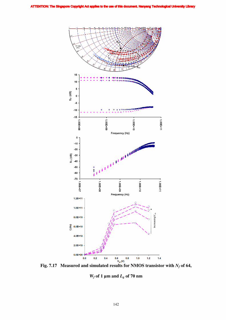
142
Fig. 7.17 Measured and simulated results for NMOS transistor with Nf of 64,
Wf of 1 µm and Lg of 70 nm
S22
S11
ATTENTION: The Singapore Copyright Act applies to the use of this document. Nanyang Technological University Library

143
Fig. 7.18 Measured and simulated results for NMOS transistor with Nf of 24,
Wf of 2.5 µm and Lg of 70 nm
S22
S11
ATTENTION: The Singapore Copyright Act applies to the use of this document. Nanyang Technological University Library

144
Fig. 7.19 Measured and simulated results for NMOS transistor with Nf of 24,
Wf of 5 µm and Lg of 70 nm
S22
S11
ATTENTION: The Singapore Copyright Act applies to the use of this document. Nanyang Technological University Library

145
Hence, as demonstrated in Fig. 7.15 to Fig. 7.19, the proposed scalable RF
model is shown to be geometry and biasing scalable for the S-parameters and fT for
the frequency range from 50 MHz to 49.85 GHz.
Basically, S11 constitutes the gate resistance and capacitance when looking
into the gate terminal. But at low frequency, S11 is dominated by the gate
capacitances and is proportional to Nf and Wf as shown in (7-10) and (7-11). From
Fig. 7.15 to Fig. 7.19, the measured S11 shows a strong capacitance behaviour
which is dependent on the transistor’s Nf and Wf. Similarly looking into port 2, the
S22 parameter consists of the diffusion and channel resistances, the drain junction
parasitics and the drain-to-gate and drain-to-source capacitances. In (7-11) and (7-
12), the drain related capacitances are shown to be directly proportional to Nf and
Wf. As the device size increases, the plotted S22 result will show a higher
capacitance curve and the biasing and geometry effect on the diffusion and channel
resistances will cause the S22 to shift in the resistance axis of the smith chart. Since
S21 is defined as the forward transmission gain, the transistor’s gain will also
increases as Nf or Wf increases and this is observed in the Fig. 7.15 to Fig. 7.19.
Generally, the magnitude of S12 is small but it should still vary with respect to Nf
and Wf and as frequency increases, the impedance of the parasitic capacitances will
drop and this will cause the reverse transmission gain to increase. The parameter fT
is shown to be proportional to gm/Cg in (5-1). Since gm and Cg is proportional to
NfWf/Lg and NfWfLg respectively, it can be derived that fT is proportional to 1/Lg2
and is independent of the transistor’s Nf and Wf. But in Fig. 7.15 to Fig. 7.19, the
measured fT plots shows slight difference as Nf and Wf varies, the differences can
be contributed by the parasitic capacitances from the test structures and also the
self-heating effect for larger size transistors that will affect the measured gm values.
ATTENTION: The Singapore Copyright Act applies to the use of this document. Nanyang Technological University Library

146
7.4 Proposed Scalable Model Verification Technique
In a scalable RFCMOS model, there are many different variables that
determined the scalability of the RF model. The developed model file has to be
scalable for a certain range of geometry, biasing and frequency variables. In the
past, the conventional way to verify the accuracy of a model provided by the
foundry is by monitoring the simulated and measured plots for the DC, S-
parameters and fT. If the conventional method is used for verifying the scalable
RFCMOS model, there will be many plots that are required to be generated and it
will be very tedious to verify the scalable model’s accuracy. Furthermore,
presently there is no published methodology as of how to quantify the developed
model’s accuracy provided by the foundry. Hence, a new technique is proposed
here to verify the scalability and quantify the accuracy of RFCMOS models. This
proposed verification technique is crucial to both the modeling engineers and the
model file end users as it helps them to monitor the quality of the developed model
and at the same time, the model file can be checked for any errors in the coded
geometry equations of the parasitic sub-circuit components. Furthermore by using
this proposed technique, the amount of verification time required to check the
developed model file is reduced and thus reducing the overall model development
time.
In this proposed technique, the model accuracy and continuity plots are
generated to monitor the device geometry, biasing and frequency variables of the
RF model. From these two types of plots, the quality of the developed model and
the coded model file will be inspected and the final verified model file will be error
free and reliable to use.
ATTENTION: The Singapore Copyright Act applies to the use of this document. Nanyang Technological University Library

147
Fig. 7.20 Model Accuracy for NMOSFETs with different Nf and Wf of 1, 2.5
and 5 µm at Vgs = 0.95 V and Vds = 0.8 V
Fig. 7.20 shows the model accuracy plots for NMOS transistors with
different values of Nf, of 4, 8, 16, 24, 32, 48 and 64 and Wf of 1, 2.5 and 5 µm
extracted at Vgs = 0.95 V and Vds = 0.8 V respectively. The calculated absolute
errors between the measured and simulated data for the DC characteristics, S-
parameters and fT at the various frequency points are presented in the model
accuracy plot. The DC characteristics include the extracted drain current, Gm and
Rout while the 2-port S-parameters (S11, S12, S21 and S22) are extracted at the three
frequency points of interest. For the extraction of the transistor’s fT, the
extrapolation method is used at the same frequency points as the S-parameters. If it
is desired to check the higher frequency range, more column of box plot can be
incorporated into the model accuracy plot but more time will be required to collect
these data to generate the accuracy plot for model verification.
ATTENTION: The Singapore Copyright Act applies to the use of this document. Nanyang Technological University Library
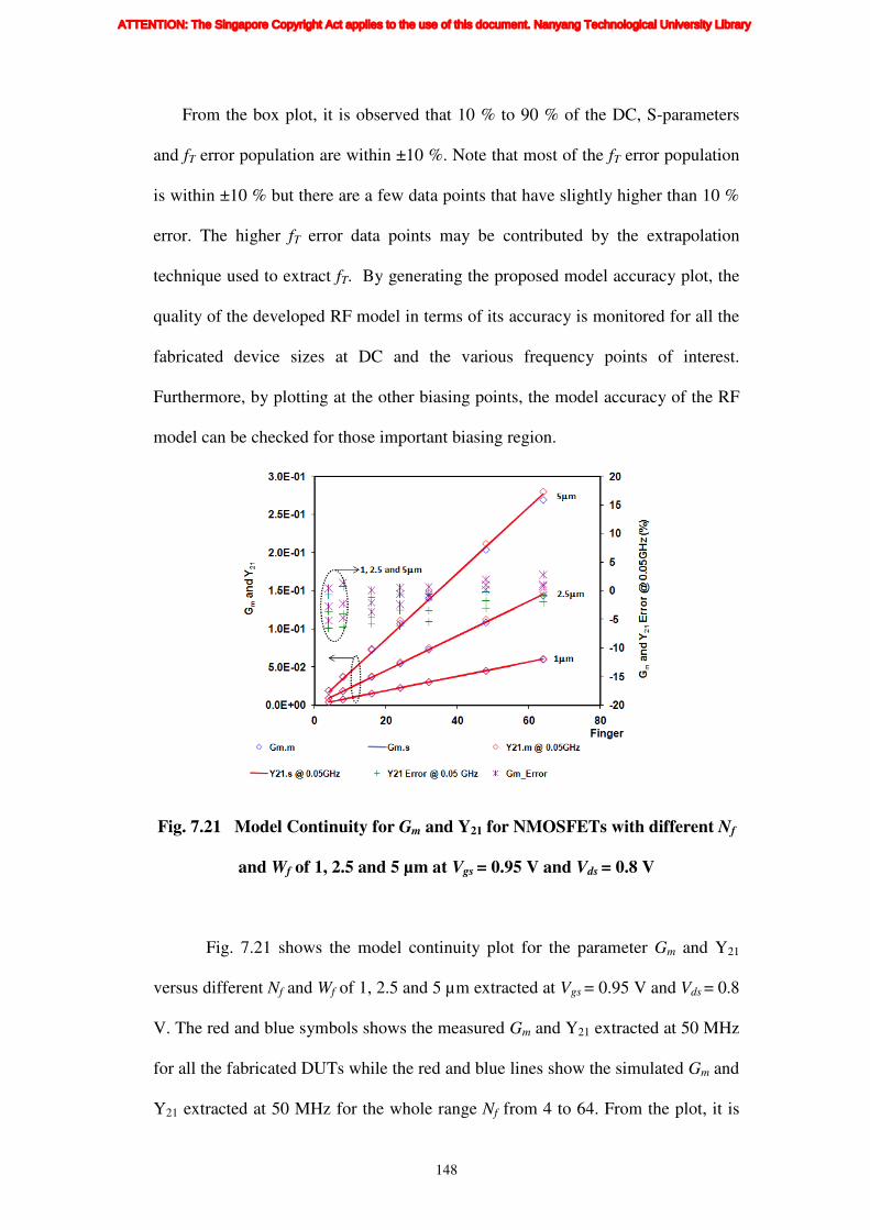
148
From the box plot, it is observed that 10 % to 90 % of the DC, S-parameters
and fT error population are within ±10 %. Note that most of the fT error population
is within ±10 % but there are a few data points that have slightly higher than 10 %
error. The higher fT error data points may be contributed by the extrapolation
technique used to extract fT. By generating the proposed model accuracy plot, the
quality of the developed RF model in terms of its accuracy is monitored for all the
fabricated device sizes at DC and the various frequency points of interest.
Furthermore, by plotting at the other biasing points, the model accuracy of the RF
model can be checked for those important biasing region.
Fig. 7.21 Model Continuity for Gm and Y21 for NMOSFETs with different Nf
and Wf of 1, 2.5 and 5 µm at Vgs = 0.95 V and Vds = 0.8 V
Fig. 7.21 shows the model continuity plot for the parameter Gm and Y21
versus different Nf and Wf of 1, 2.5 and 5 µm extracted at Vgs = 0.95 V and Vds = 0.8
V. The red and blue symbols shows the measured Gm and Y21 extracted at 50 MHz
for all the fabricated DUTs while the red and blue lines show the simulated Gm and
Y21 extracted at 50 MHz for the whole range Nf from 4 to 64. From the plot, it is
ATTENTION: The Singapore Copyright Act applies to the use of this document. Nanyang Technological University Library

149
observed that the simulated Gm (blue line) and Y21 (red line) overlaps each other
and this observation implies that the RF model is continuous from DC to RF
region. Furthermore, the simulated transistor’s gain (red and blue lines) can
accurately predict the measured data (red and blue symbols) as the Nf and Wf
changes and their calculated absolute errors are within the error specification of
±10 %. It is also observed that the simulated Gm and Y21 scale linearly with Nf for
all the three Wf. By plotting the proposed model continuity plot at other biasing
points, the Nf, Wf and biasing effect on the RF model are monitored at both the DC
and low frequency region. In the case when the coded equations of the sub-circuit
components in the model file are incorrect, the model accuracy and continuity
plots will immediately reflect the incorrect effects of the wrong equations and this
will alert the modeling engineer to check the coded model file again.
The proposed model accuracy and continuity plots can also be used as one
of the model acceptance criteria whereby its accuracy and continuity can be
checked before accepting and using the developed RF model file for circuit
simulation.
7.5 RF Noise Modeling Results
The high frequency noise model equations are implemented into the
transistor’s core models and the circuit simulators. When the implemented noise
model equations under-estimate the noise performance of the transistor [98], it is
usually very difficult for the modeling engineers to go directly into the core models
to change the model’s equations. Similar changes will also be required for the
circuit simulators to recognize the change in the noise model equations. Such
modifications to the core model and the circuit simulators can only be done by the
ATTENTION: The Singapore Copyright Act applies to the use of this document. Nanyang Technological University Library

150
software vendors. Hence, in order to compensate the under-estimation of the
compact noise models, it is proposed to add in additional noise sources into the RF
model using the sub-circuit approach [99]. In this research, the noise
implementation is done using a BSIM3v3 compact model.
7.5.1 Noise source implementation
Fig. 7.22 shows the RF equivalent circuit model with added enhanced noise
current 2
dei and induced gate noise current 2
gi . Note that the correlation noise
current *
dgii is not added into the RF model because most circuit simulators are
unable to process the correlation noise sources.
In Fig. 7.23, the component values of Rde, Rind and Cind of the implemented
noise sources are extracted using the derived equations in [99].
Although the equivalent circuit model in Fig. 7.22 is different from the
proposed equivalent circuit model in [99], similar technique to implement the
noise sources can be applied. The additional noise current 2
dei and 2
gi are
implemented with current control current source (CCCS) and their noise current is
determined by the component values of Rde, Cind and Rind at each biasing point. The
current of the CCCS is set to zero so that it will not affect the DC and AC
characteristics of the RF small-signal model. The added CCCS will only contribute
the required noise current that can compensate the under-estimation of the
BSIM3v3 model. By using Verilog-A, the CCCS can be coded with the required
biasing and geometry dependences so that scalable HF noise modeling can be
achieved. By setting up the geometry and biasing variables as shown in the
Verilog-A function in Appendix A, equations can be formed to calculate the
components values of Rde, Cind and Rind at each biasing point and geometry
ATTENTION: The Singapore Copyright Act applies to the use of this document. Nanyang Technological University Library

151
combination. HF noise simulation is then setup to simulate the model file with the
Verilog-A function to obtain the simulated HF noise parameters for comparison
with the measured data.
Fig. 7.22 RF equivalent circuit model with added enhanced noise current
2
dei and induced gate noise current 2
gi
(a) (b)
Fig. 7.23 Equivalent noise circuit (a) 2
dei and (b) 2
gi that generate additional
noise current [99]
ATTENTION: The Singapore Copyright Act applies to the use of this document. Nanyang Technological University Library
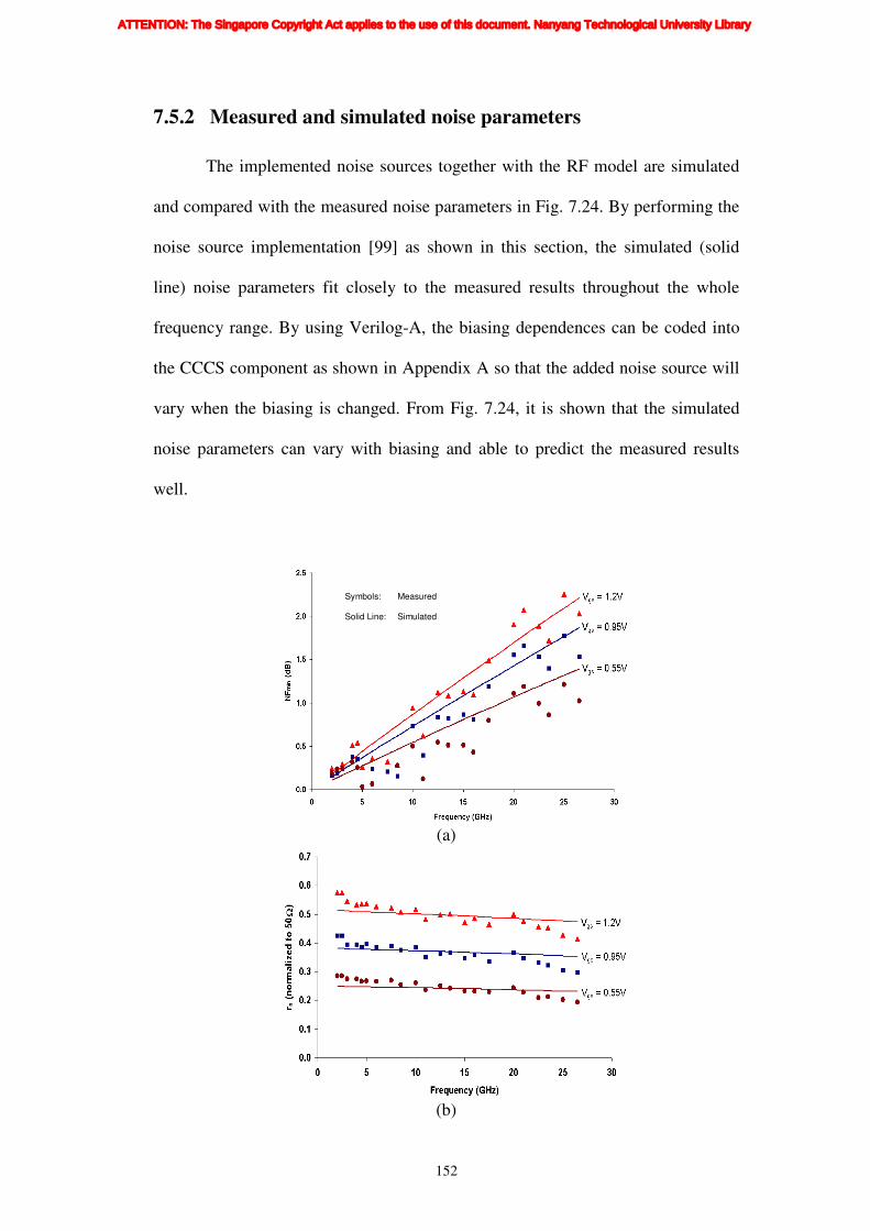
152
7.5.2 Measured and simulated noise parameters
The implemented noise sources together with the RF model are simulated
and compared with the measured noise parameters in Fig. 7.24. By performing the
noise source implementation [99] as shown in this section, the simulated (solid
line) noise parameters fit closely to the measured results throughout the whole
frequency range. By using Verilog-A, the biasing dependences can be coded into
the CCCS component as shown in Appendix A so that the added noise source will
vary when the biasing is changed. From Fig. 7.24, it is shown that the simulated
noise parameters can vary with biasing and able to predict the measured results
well.
(a)
(b)
Symbols: Measured
Solid Line: Simulated
ATTENTION: The Singapore Copyright Act applies to the use of this document. Nanyang Technological University Library

153
(c)
(d)
Fig. 7.24 Measured (symbol) and simulated (solid line) noise parameters
versus frequency for transistor with Nf of 32, Wf of 5 µµµµm and Lg of 70 nm
(Extracted Vds= 1.2 V @ Vgs= 0.55, 0.95 and 1.2 V)
In order to demonstrate the accuracy of the generated HF noise model, the
simulated noise circles (dotted line) and the measured noise figures (symbol) at the
other source impedance states are also plotted in Fig. 7.25. It is observed that the
simulated noise circles can closely predict the measured noise figures at various
source impedance states. Thus, it demonstrates the accuracy of the simulated noise
parameters.
ATTENTION: The Singapore Copyright Act applies to the use of this document. Nanyang Technological University Library

154
0.2
0.5
1.0
2.0
5.0
+j0.2
-j0.2
+j0.5
-j0.5
+j1.0
-j1.0
+j2.0
-j2.0
+j5.0
-j5.0
0.0
1.17
2.31
0.71
1.11
1.14
4.02
5.08
4.97
4.67
2.62
1.18
0.4
1.48
1.72
2.29
4.67
ΓΓΓΓopt
Fig. 7.25 Simulated noise circles and measured noise figures at different
source impedance states for transistor with Nf of 32, Wf of 5 µµµµm and Lg of 70
nm (Extracted at Vds= 1.2 V, Vgs= 0.55 V and frequency = 5 GHz)
7.6 Summary
In this chapter, the physical formation of the sub-circuit parasitic is
discussed with respect to its layout structure. The scaling effect of the device
geometry is accounted for in the proposed scalable equations for each of the
parasitic components. By implementing the proposed scalable equation for the
parasitic components into the conventional sub-circuit RF model, a scalable
RFCMOS sub-circuit model can be generated and shown to be valid up to 49.85
GHz. Although the proposed equation of the parasitic sub-circuit components are
classical, which mainly make use of the material’s sheet resistance and capacitance
5dB 4dB 3dB 2dB 1dB
ATTENTION: The Singapore Copyright Act applies to the use of this document. Nanyang Technological University Library

155
per unit area but in this chapter, it has demonstrated that such simple equations are
sufficient to model the parasitic components when the transistor geometry layout
changes. Furthermore, in most of the reported papers, the parasitic equations are
usually not compiled and discussed in a single publication and the accuracy of the
model is usually demonstrated with one or two device’s sizes. However, in this
chapter, all of the sub-circuit parasitic are discussed and formulated and the
scalable sub-circuit model is simulated with frequency for a range of Nf, Wf and
biasing points. The excellent fitting between the measured and simulated results
shows that the generated scalable RF model is scalable for the range of the
transistor’s Nf, Wf and biasing points.
By using the proposed verification technique, the time required to verify a
scalable RFCMOS model can be reduced greatly and the verification step can also
ensure that the developed model is error free. Therefore, it is more robust and
reliable to use in RF circuit design. It is shown that by implementing the noise
sources using Verilog-A in section 7.5, the biasing and geometry dependence of
the noise parameters can be predicted accurately as presented in Fig.7.24 and Fig.
7.25.
ATTENTION: The Singapore Copyright Act applies to the use of this document. Nanyang Technological University Library
156
Chapter 8
A SCALABLE RFCMOS NOISE MODEL
8.1 Introduction
The geometry scalability of RFCMOS models have allowed circuit
designers to have more flexibility in choosing the device sizes that they need in the
circuit design. However, the model simulation capability for the transistor’s high
frequency (HF) noise performance is still limited by the BSIM core model that
under-estimates the HF noise for short channel devices. In order to obtain accurate
HF noise simulation, noise sources are proposed to be added into the RF model to
compensate the under-estimation from the BSIM core model. By monitoring the
trend of the noise sources and implementing them using Verilog-A, accurate and
scalable HF noise modeling can be achieved. Furthermore, the scalable HF noise
model allows more powerful PDK to be developed so that the optimum device size
based on its DC, S-parameters and noise performances can be selected to use in
critical RF block such as the low noise amplifier (LNA).
Although HF noise modeling has been widely studied and researched, in
most of the published papers, they mainly demonstrated HF noise model fitting at
a fixed device size and a few biasing points [71], [98]-[102]. The objective of this
research is to demonstrate scalable HF noise modeling for RFCMOS transistor for
a wide range of geometry sizes, biasing and frequency points. In this chapter, a
brief review on the measurement theory is presented to study the measurement
setup limitations that may explain the irregular fluctuation of the measured NFmin
versus frequency for small device sizes and low biasing points. By using a Matlab
ATTENTION: The Singapore Copyright Act applies to the use of this document. Nanyang Technological University Library

157
program, the pads and interconnects noise are de-embedded to obtain the true
device noise parameters. The extracted noise sources versus the transistor’s
geometry and biasing points can be plotted and explained by using the classical RF
noise model and this further proves that the extracted noise sources results are
reliable. Finally, by simulating the scalable HF noise model, the measured and
simulated noise parameters are plotted for a range of geometry, biasing and
frequency points. In addition to demonstrate the accuracy of the developed noise
model, the measured noise figures at other source impedance states are plotted
together with the simulated noise circles in the smith chart.
8.2 HF Noise Measurement and Parasitic De-embedding
8.2.1 Test setup and parasitic de-embedding
The measurement system ATN NP5 is used for HF noise and S-parameters
measurement and its setup is as shown in Fig. 3.12. The frequency module of 2 to
26.5 GHz was used. In this study, the devices under test (DUT) are thin gate
NMOS transistors that have a fixed channel length (Lg) of 70 nm, unit width (Wf)
of 1, 2.5 and 5 µm and finger number (Nf) of 4, 16, 32, and 64. The RF transistor
and its standard OPEN and SHORT de-embedding structures were measured at
various bias combinations of the gate to source (Vgs) and drain to source (Vds)
potentials for a range of frequency points. By using the reported technique in [76]
and [77], the pads and interconnects parasitic that contributed to the measured HF
noise and S-parameters can be removed to obtain the intrinsic transistor
characteristics.
ATTENTION: The Singapore Copyright Act applies to the use of this document. Nanyang Technological University Library

158
(a)
(b)
Fig. 8.1 Noise parameters (a) NFmin and rn and (b) real(ΓΓΓΓopt) and imag(ΓΓΓΓopt)
before (solid line) and after (symbols) de-embedding of the pads and
interconnects parasitic for transistor with Nf of 32, Wf of 5 µµµµm and Lg of 70
nm at Vgs = 0.95 V and Vds = 1.2 V
ATTENTION: The Singapore Copyright Act applies to the use of this document. Nanyang Technological University Library

159
Fig. 8.1 shows the four noise parameters before and after de-embedding of
the pads and interconnects parasitic. It is shown that the effect of the pads and
interconnects affect the noise parameters slightly. This is because in the test
structures, the design of the pads and interconnects are shielded with ground metal
and it has been published in the literature that such layout design is capable of
shielding the wafer surface from the substrate’s noise that can degrade the
measured noise figure of the DUT [103].
Fig. 8.2 Simplified RF NMOS layout
Fig. 8.2 shows the simplified layout of the RF NMOS transistor. The
transistor has a multi-finger configuration with double contacted gate poly
structure. Dummy gate poly is added to improve the gate structure formation and
metals 1 and 2 are used for the connection of the gate terminal. The source
diffusions are connected using the metal 1 layer and shorted to the body terminal
or P-well while the drain diffusions are pulled out using the metal 3 layer.
ATTENTION: The Singapore Copyright Act applies to the use of this document. Nanyang Technological University Library
160
8.2.2 ATN NP5 measurement theory
Basically, the transistor’s noise figure (F) is dependent on the four noise
parameters and the source reflection coefficient (Γs) as shown in (8-1).
( ) 22
2
min
11
4
opts
optsnrFF
Γ+⋅Γ−
Γ−Γ⋅+=
⋅ (8-1)
The variable Fmin is the linear term of minimum noise figure when the
complex source reflection coefficient (Γs) is matched to the optimum complex
source reflection coefficient (Γopt) and rn is the normalized noise resistance which
is a measure of how sensitive the transistor’s noise figure to the source mismatch
from Γopt. It is obvious that for low noise transistor performance smaller Fmin and rn
are desirable. From (8-1), the noise parameters that need to be extracted are Fmin, rn
and the real and imaginary terms of Γopt. In principle, since four variables are
required to be extracted, only four measurements at different Γs are required. But
in practice, sixteen measurements are done to increase the accuracy of the noise
parameters extraction.
During the noise measurement, the measured noise figure includes both the
measurement system and the DUT. In order to obtain the noise parameters of the
DUT, the noise contribution from the measurement system (Fsys) has to be
determined during the calibration stage so that it can be removed automatically by
the measurement software. During noise measurement, the total noise figure (Ftotal)
at different source impedance states is measured and by using the Friss cascade
equation [80] in (8-2), the DUT noise figure (Fdut) can be calculated. Note that Gdut
is the available gain of the DUT.
ATTENTION: The Singapore Copyright Act applies to the use of this document. Nanyang Technological University Library

161
dut
sys
totaldutG
FFF
1−−= (8-2)
As the ATN measurement system uses Friss equation to extract the noise
figure of the DUT, the measurement accuracy will be greatly dependent on the
measured Gdut. For example, if Fsys is large and Gdut is small, the second term in (8-
2) will be large and Fdut will be the subtraction of two large numbers; hence this
will lead to Fdut to be very sensitive to measurement errors. Furthermore, the
accuracy of measured Fdut will in turn affect the extraction of Fmin parameter in (8-
1). Therefore, it is expected that for measurement of small device sizes with low
Gdut values, their Fmin are typically less than 1 dB. Thus, the extraction of Fmin will
be a challenge under such conditions.
(a)
ATTENTION: The Singapore Copyright Act applies to the use of this document. Nanyang Technological University Library

162
(b)
Fig. 8.3 Noise parameters (a) NFmin and rn and (b) real(ΓΓΓΓopt) and imag(ΓΓΓΓopt)
before (solid line) and after (symbols) de-embedding for transistor with Nf of
32, Wf of 1 µµµµm and Lg of 70 nm at Vgs = 0.95 V and Vds = 1.2 V
Fig. 8.3 shows the extracted noise parameters for a transistor with Nf of 32,
Wf of 1 µm and Lg of 70 nm. The extraction of the noise parameters were done at
the same biasing condition as in Fig. 8.1. It is shown that the extracted NFmin
becomes fluctuating and doesn’t have a clear upward trend with respect to the
frequency. However, the extraction of the parameter rn and Γopt are not affected in
the measurement. It is suspected that such extracted behavior of the NFmin
parameter is due to the measurement limitation of the ATN system as discussed in
(8-2). Hence, due to the measurement system limitation, the extraction of the NFmin
for small device sizes and low biasing points will have such irregular trend of
NFmin versus frequency.
ATTENTION: The Singapore Copyright Act applies to the use of this document. Nanyang Technological University Library

163
Fig. 8.4 shows the measured and simulated DC characteristics for the
transistor with Nf of 32, Wf of 1 µm and Lg of 70 nm. The measured DC results
show that the device used for the noise measurement is operating correctly.
Another possible explanation for the fluctuation in the extracted NFmin is that the
source impedance state used for the noise measurement falls either in the
“conditionally stable” or “unstable” region. This will cause errors in the measured
noise figures for each of the source impedance states during the noise
measurement. As the NFmin is extracted from these measured noise figures, the
fitted NFmin curve may contain such errors and cause it to fluctuate as shown in
Fig. 8.3(a).
(a)
ATTENTION: The Singapore Copyright Act applies to the use of this document. Nanyang Technological University Library

164
(b)
Fig. 8.4 DC characteristics (a) gm versus Vgs and (b) Ids versus Vds with
measured (symbols) and simulated (solid line) data for transistor with Nf of
32, Wf of 1 µµµµm and Lg of 70 nm
8.3 Noise Source Extraction
Fig. 8.5 Proposed RFCMOS model with extrinsic parasitic resistance noise,
intrinsic induced gate noise ( 2
gi ) and channel thermal noise ( 2
di )
ATTENTION: The Singapore Copyright Act applies to the use of this document. Nanyang Technological University Library

165
Fig. 8.5 shows a RFCMOS model that has all the extrinsic parasitic
components and their corresponding resistance noise, the intrinsic induced gate
( 2
gi ) and channel thermal ( 2
di ) noise sources. By using the reported noise source
extraction technique in [104], the intrinsic noise source, 2
gi , 2
di and their cross-
correlation term ( *
dgii ) can be extracted from the measured S-parameters and noise
measurements. In this extraction technique, the measured noise parameters are de-
embedded from its pads and interconnect noise and by using the correlation matrix
in [105] and [106], the extrinsic parasitic resistance noise sources can be de-
embedded and obtain the intrinsic noise portion as indicated in Fig. 8.5. The 2
gi , 2
di
and *
dgii can be calculated using the equations given in [104]. As the extraction
technique uses the extrinsic resistances for the noise de-embedding, the accuracy
of the extracted 2
gi , 2
di and *
dgii will strongly dependent on the accuracy of the
extrinsic resistances values. Hence, it is crucial that the small-signal RF transistor
model must be modeled accurately before the noise source extraction can be done.
In the classical RF noise model from Van Der Ziel [54], [55], the
expression for 2
di and 2
gi are given as shown in (8-3) and (8-4) respectively.
fgkTi dd ∆= 0
2 4 γ (8-3)
fg
CkTi
d
gsg ∆
=
0
22
2
54
ωδ (8-4)
22*
dgdg iicii ⋅= (8-5)
In (8-3), the parameter gdo is the drain-source conductance at zero Vds. γ is
the noise factor and has a value of unity at zero Vds. In long channel devices, γ
ATTENTION: The Singapore Copyright Act applies to the use of this document. Nanyang Technological University Library

166
decreases to a value of 2/3 in saturation region. Note that for short channel devices
that operate in saturation region, γ can be considerably higher than the long
channel value. In (8-4), the parameter δ is the gate noise coefficient and it is given
a value of 4/3 in [54]. The factor c in (8-5) represents the correlation between the
noise 2
di and 2
gi . By studying the geometry dependence of gdo and Cgs in (8-3) and
(8-4), it is found that 2
di , 2
gi and *
dgii is proportional tog
ff
L
WN,
3
gff LWN and
gff LWN respectively. Furthermore in terms of frequency (f) dependences, it is
clear that 2
di is frequency independent while 2
gi and *
dgii is proportional to 2f and
f respectively. The frequency and geometry dependences plots for the noise
sources are shown in Figs. 8.6 and 8.7. The plots in Figs. 8.6 and 8.7 clearly
validate the above discussion on the frequency and geometry dependences of the
noise sources.
(a)
ATTENTION: The Singapore Copyright Act applies to the use of this document. Nanyang Technological University Library
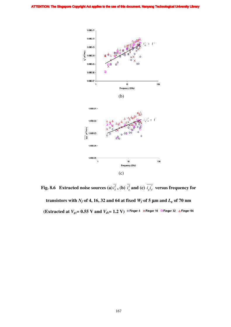
167
(b)
(c)
Fig. 8.6 Extracted noise sources (a) 2
di , (b) 2
gi and (c) *
dgii versus frequency for
transistors with Nf of 4, 16, 32 and 64 at fixed Wf of 5 µµµµm and Lg of 70 nm
(Extracted at Vgs= 0.55 V and Vds= 1.2 V)
ATTENTION: The Singapore Copyright Act applies to the use of this document. Nanyang Technological University Library
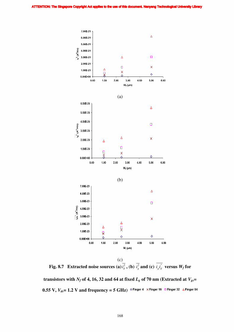
168
(a)
(b)
(c)
Fig. 8.7 Extracted noise sources (a) 2
di , (b) 2
gi and (c) *
dgii versus Wf for
transistors with Nf of 4, 16, 32 and 64 at fixed Lg of 70 nm (Extracted at Vgs=
0.55 V, Vds= 1.2 V and frequency = 5 GHz)
ATTENTION: The Singapore Copyright Act applies to the use of this document. Nanyang Technological University Library

169
(a)
(b)
(c)
Fig. 8.8 Extracted noise sources (a) 2
di , (b) 2
gi and (c) *
dgii versus Vgs for
transistors with Nf of 4, 16, 32 and 64 at fixed Wf of 5 µµµµm and Lg of 70 nm
(Extracted at Vds= 1.2 V and frequency = 5 GHz)
ATTENTION: The Singapore Copyright Act applies to the use of this document. Nanyang Technological University Library

170
The biasing dependence of the extracted noise sources 2
di , 2
gi and *
dgii is
shown in Fig. 8.8. It is shown that 2
di increases with Vgs as in Fig. 8.8(a). This is
mainly due to the higher output conductance when Vgs increases at a fixed Vds
biasing point [100]. As 2
gi is mainly the coupled thermal noise from the channel
through the gate capacitance to the gate structure, it is strongly dependent on the
gate capacitance and is less sensitive to the biasing applied in the channel. Hence
in Fig. 8.8(b), it shows that 2
gi has little changes when Vgs increases. Note that the
correlation noise *
dgii follows the Vgs dependence of 2
di .
8.4 High Frequency Noise Modeling
In most compact models, their high frequency noise model equations are
implemented into their core models and circuit simulators are designed to
recognize these model equations when it perform simulations using these models.
When the implemented noise model equations under-estimate the noise
performance of the transistor [98], it is usually very difficult for modeling
engineers to go into the core models to change the model’s equations and such
changes may require similar modifications to be done on the device simulators
which only the software vendor can carry out. Hence, in order to compensate the
under-estimation of the compact noise models, it is proposed to add in additional
noise sources into the RF model using the sub-circuit approach [99]. In this study,
the noise implementation is done using a BSIM3v3 compact model.
ATTENTION: The Singapore Copyright Act applies to the use of this document. Nanyang Technological University Library

171
8.4.1 Noise source implementation
Fig. 8.9 RF equivalent circuit model with added enhanced noise current
2
dei and induced gate noise current 2
gi
Fig. 8.9 shows the RF equivalent circuit model with added enhanced noise
current 2
dei and induced gate noise current 2
gi . Note that the correlation noise
current *
dgii is not added into the RF model because most circuit simulators are
unable to process the correlation noise sources.
ATTENTION: The Singapore Copyright Act applies to the use of this document. Nanyang Technological University Library

172
(a)
(b)
Fig. 8.10 Equivalent noise circuit (a) 2
dei and (b) 2
gi that generate additional
noise current [99]
In [99], the following equations are derived to extract the component
values of Rde, Rind and Cind of the equivalent noise circuits as shown in Fig. 8.10.
22
4
dBSIMd
de
ii
kTR
−= (8-6)
πkT
fPC ind
ind8
100 max⋅⋅= (8-7)
2216 ind
ind
indCkT
PR
π= (8-8)
2
2
f
iP
g
ind = (8-9)
Note that 2
dBSIMi is the simulated channel thermal noise current of the
BSIM3v3 core model and maxf is the maximum frequency for the noise model to
be valid.
ATTENTION: The Singapore Copyright Act applies to the use of this document. Nanyang Technological University Library

173
Although the equivalent circuit model of Fig. 8.9 is different from the
proposed equivalent circuit model in [99], similar technique to implement the
noise sources can be applied. The additional noise current 2
dei and 2
gi are
implemented with current control current source (CCCS) and their noise current is
determined by the component values of Rde, Cind and Rind at each biasing point. The
current of the CCCS is set to zero so that it will not affect the DC and AC
characteristics of the RF small-signal model. The added CCCS will only contribute
the required noise current that can compensate the under-estimation of the
BSIM3v3 model. By using Verilog-A, CCCS can be coded with the required
biasing and geometry dependences so that scalable HF noise modeling can be
achieved.
The same modeling approach for the scalable HF noise model can be
applied to the RF circuit design tools such as Cadence, Advanced Design System
(ADS) and Microwave Office (MWO). In their circuit simulators, the CCCS
component can be described with geometry and biasing equations and they are
added into the RFCMOS model to generate the required additional noise current
during the HF noise simulation. Therefore, accurate and scalable HF noise
simulation can be achieved and give better prediction for noise performance of the
designed RF circuit blocks.
8.4.2 Measured and simulated noise parameters
The implemented noise sources together with the RF model are simulated
and compared with the measured noise parameters in Fig. 8.11. In this simulation,
the Cadence Spectre simulator is used for the simulation of the HF noise
parameters.
ATTENTION: The Singapore Copyright Act applies to the use of this document. Nanyang Technological University Library
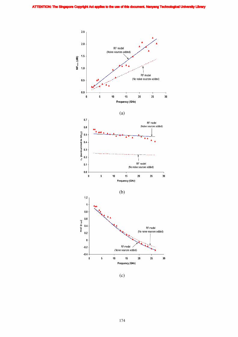
174
(a)
(b)
(c)
ATTENTION: The Singapore Copyright Act applies to the use of this document. Nanyang Technological University Library

175
(d)
Fig. 8.11 Measured (symbol) and simulated (solid and dash line) noise
parameters versus frequency for transistor with Nf of 32, Wf of 5 µµµµm and Lg of
70 nm (Extracted at Vgs= 1.2 V and Vds= 1.2 V)
(a)
(b)
ATTENTION: The Singapore Copyright Act applies to the use of this document. Nanyang Technological University Library

176
(c)
Fig. 8.12 Measured (symbol) and simulated (solid line) noise parameters
versus frequency for transistor with Nf of 32, Wf of 5 µµµµm and Lg of 70 nm
(Extracted Vds= 0.5 V @ Vgs= 0.55, 0.95 and 1.2 V)
(a)
(b)
ATTENTION: The Singapore Copyright Act applies to the use of this document. Nanyang Technological University Library

177
(c)
Fig. 8.13 Measured (symbol) and simulated (solid line) noise parameters
versus frequency for transistor with Nf of 32, Wf of 5 µµµµm and Lg of 70 nm
(Extracted Vds= 1.2 V @ Vgs= 0.55, 0.95 and 1.2 V)
Fig. 8.11 provides a comparison between the measured and simulated noise
parameters versus frequency for transistor with Nf of 32, Wf of 5 µm and Lg of 70
nm. It is observed that the simulated (dash line) noise parameters for the RF model
with no additional noise sources added under-estimated the following noise
parameters NFmin, rn and imag(Γopt). By performing the noise source
implementation [99] as shown in this section, the simulated (solid line) noise
parameters fit closely to the measured results throughout the whole frequency
range. By using Verilog-A, the Vgs and Vds biasing dependences can be coded into
the CCCS component so that the added noise source will vary when the biasing is
changed. The biasing dependences of the noise parameters are shown in Figs. 8.12
and 8.13. It is shown that the simulated noise parameters can vary with biasing and
able to predict the measured results well.
ATTENTION: The Singapore Copyright Act applies to the use of this document. Nanyang Technological University Library

178
0.2
0.5
1.0
2.0
5.0
+j0.2
-j0.2
+j0.5
-j0.5
+j1.0
-j1.0
+j2.0
-j2.0
+j5.0
-j5.0
0.0
1.17
2.31
0.71
1.11
1.14
4.02
5.08
4.97
4.67
2.62
1.18
0.4
1.48
1.72
2.29
4.67
ΓΓΓΓopt
(a)
0.2
0.5
1.0
2.0
5.0
+j0.2
-j0.2
+j0.5
-j0.5
+j1.0
-j1.0
+j2.0
-j2.0
+j5.0
-j5.0
0.0
2.08
3.87
1.36
2.08
1.95
5.99
7.53
7.27
6.85
4.09
1.88
0.89
2.81
2.85
3.74
6.97
ΓΓΓΓopt
(b)
Fig. 8.14 Simulated noise circles and measured noise figures at different
source impedance states for transistor with Nf of 32, Wf of 5 µµµµm and Lg of 70
nm (a) Vds= 1.2 V, Vgs= 0.55 V and (b) Vds= Vgs= 1.2 V (Extracted at frequency
= 5 GHz)
5dB 4dB 3dB 2dB 1dB
5dB 4dB 3dB 2dB 1dB
ATTENTION: The Singapore Copyright Act applies to the use of this document. Nanyang Technological University Library

179
In order to demonstrate the accuracy of the generated HF noise model, the
simulated noise circles (dotted line) and the measured noise figures (symbol) at the
other source impedance states are plotted in Fig. 8.14. It is observed that the
simulated noise circles can closely predict the measured noise figures at various
source impedance states. Thus, it demonstrates the accuracy of the simulated noise
parameters.
Due to the possibility of measurement system limitation as discussed in the
section 8.2.2, it is very difficult to measure very good NFmin data for small width
devices at the various biasing conditions. However, it is shown in Fig. 8.3 that the
measured parameters rn and Γopt are not affected in the measurement. Therefore, in
order to show the geometry scalability of the developed HF noise model, the
simulated noise circles for the small devices are plotted with their measured noise
figures at the other source impedance states for comparison. As rn and Γopt are not
affected by the measurement system, its geometry (Nf and Wf) and biasing
dependences are plotted to show the scalability of the developed HF noise model.
Note that in the comparison of the measured noise figures with the simulated noise
circles plot, the sixteen source impedance states are selected from a full set of three
hundred and fifty three impedance states pre-determined by the mismatch noise
source at each frequency point and the selection criteria is fully controlled by the
measurement software. Hence, the selected sixteen states for each frequency point
may not be the same states for all the different device measurement at each biasing
point.
ATTENTION: The Singapore Copyright Act applies to the use of this document. Nanyang Technological University Library

180
0.2
0.5
1.0
2.0
5.0
+j0.2
-j0.2
+j0.5
-j0.5
+j1.0
-j1.0
+j2.0
-j2.0
+j5.0
-j5.0
0.0 ∞
12.88
14.81
15.94
10.43
11.77
13.57
20.48
20.69
17.75
14.69
7.6
12.17
16.45
20.18
20.71
20.03
ΓΓΓΓopt
(a)
(b)
20dB 16dB 12dB
10dB
10dB 8dB 6dB 4dB 2dB
8dB
ATTENTION: The Singapore Copyright Act applies to the use of this document. Nanyang Technological University Library

181
0.2
0.5
1.0
2.0
5.0
+j0.2
-j0.2
+j0.5
-j0.5
+j1.0
-j1.0
+j2.0
-j2.0
+j5.0
-j5.0
0.0 ∞
9.28
11.1
12.21
7.05
8.29
9.9
16.67
16.85
13.92
10.93
4.65
8.71
12.69
16.36
16.87
16.18
ΓΓΓΓopt
(c)
(d)
16dB 12dB 8dB
6dB
6dB 5dB 4dB 3dB 2dB
4dB
ATTENTION: The Singapore Copyright Act applies to the use of this document. Nanyang Technological University Library

182
0.2
0.5
1.0
2.0
5.0
+j0.2
-j0.2
+j0.5
-j0.5
+j1.0
-j1.0
+j2.0
-j2.0
+j5.0
-j5.0
0.0 ∞
6.96
8.62
9.72
5.01
6.13
7.48
14.07
14.18
11.28
8.37
3.03
6.57
10.13
13.74
14.22
13.5
ΓΓΓΓopt
(e)
0.2
0.5
1.0
2.0
5.0
+j0.2
-j0.2
+j0.5
-j0.5
+j1.0
-j1.0
+j2.0
-j2.0
+j5.0
-j5.0
0.0 ∞
1.34
2.88
1.03
1.69
0.92
4.04
6.49
5.68
5.05
2.22
0.49
1.11
2.71
1.53
2.39
5.68
ΓΓΓΓopt
(f)
Fig. 8.15 Simulated noise circles and measured noise figures at different
source impedance states for transistor (a) Nf = 4, Wf = 1 µµµµm, (b) Nf = 64, Wf =
1 µµµµm, (c) Nf = 4, Wf = 2.5 µµµµm, (d) Nf = 64, Wf = 2.5 µµµµm, (e) Nf = 4, Wf = 5 µµµµm
and (f) Nf = 64, Wf = 5 µµµµm at fixed Lg of 70 nm (Extracted at Vgs = Vds = 1.2 V
and frequency = 5 GHz)
4dB
5dB 4dB 3dB 2dB 1dB
14dB 10dB 8dB 6dB
ATTENTION: The Singapore Copyright Act applies to the use of this document. Nanyang Technological University Library

183
Fig. 8.15 shows the simulated noise circles and measured noise figures at
the other source impedance states for various transistors’ geometry Nf and Wf. It
has shown that the simulated noise circles can predict accurately for small (Nf of 4
with Wf of 1, 2.5 and 5 µm) and large (Nf of 64 with Wf of 1, 2.5 and 5 µm)
transistors. This further demonstrates that all the noise parameters NFmin, rn and
Γopt are simulated accurately for the above geometry range.
In Figs. 8.16 and 8.17, the measured and simulated noise parameters rn and
Γopt are plotted versus biasing and transistor’s geometry respectively. Both figures
show that the simulated results can predict the measured values for the above range
of biasing, Nf and Wf. Therefore, from the plots presented in Figs. 8.12 to 8.17, it
has demonstrated that a scalable HF noise model was achieved in this work for
various biasing and transistor’s geometry.
(a)
ATTENTION: The Singapore Copyright Act applies to the use of this document. Nanyang Technological University Library
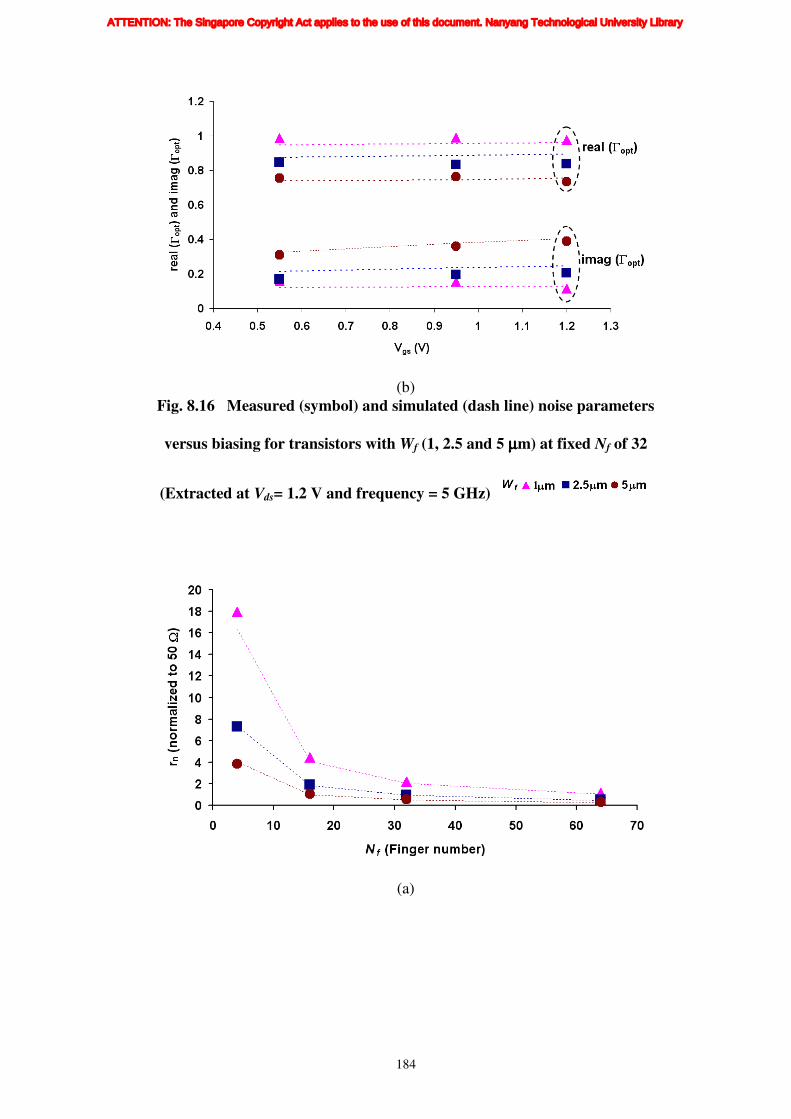
184
(b)
Fig. 8.16 Measured (symbol) and simulated (dash line) noise parameters
versus biasing for transistors with Wf (1, 2.5 and 5 µµµµm) at fixed Nf of 32
(Extracted at Vds= 1.2 V and frequency = 5 GHz)
(a)
ATTENTION: The Singapore Copyright Act applies to the use of this document. Nanyang Technological University Library

185
(b)
Fig. 8.17 Measured (symbol) and simulated (dash line) noise parameters
versus transistors’ geometry with Nf (4, 16, 32 and 64) and Wf (1, 2.5 and 5
µµµµm) (Extracted at Vgs= Vds= 1.2 V and frequency = 5 GHz)
8.5 Summary
The HF noise model is normally demonstrated for one or few device sizes
and some biasing points for a range of frequency in most reported works. But in
order for the HF noise model to be applicable to the industry, it has to be able to
simulate for a wide range of geometry, biasing and frequency points. Hence, in this
research, the scalability of the HF noise model is demonstrated with excellent
accuracy for up to 26 GHz for the four key noise parameters, i.e., NFmin, rn,
real(Γopt) and imag(Γopt) at different geometrical combination of Nf and Wf, and at a
broad range of biasing points.
ATTENTION: The Singapore Copyright Act applies to the use of this document. Nanyang Technological University Library

186
Furthermore, to show the accuracy of the developed scalable HF noise
model, its simulated noise circles are plotted against the measured noise figures at
other source impedance states. Very good fit is achieved between the measured
and simulated results. The effect of the metal ground shielding on the pads and
interconnects shows that it is able to shield the transistor from the substrate noise
sources. The fluctuating of the measured NFmin versus frequency trend for the
small devices is explained with the measurement theory and set-up. Although the
NFmin parameter is fluctuating with frequency, the other three noise parameters (rn,
real(Γopt) and imag(Γopt)) can be used to demonstrate the HF noise model fitting
between the simulated and the measured results.
Finally, the scalability of the HF noise model can help circuit designers to
optimize their designs and run accurate simulations to ensure circuit performances
are within the chip specifications before sending them for fabrication. This can
greatly enhance the chance of first time success in tape-out and reduce the design
cycle time for RF chips that have critical noise requirements.
ATTENTION: The Singapore Copyright Act applies to the use of this document. Nanyang Technological University Library

187
Chapter 9
CONCLUSIONS AND RECOMMENDATIONS
9.1 Conclusions
The relentless improvement in CMOS technology has greatly improved its
RF characteristics which make it a viable technology for realizing many RF
applications. But to optimize the current circuit design process, RF models
development must also be improved. Currently, most foundries provide discrete
sizes for RF models in their PDK and this will limit the device selection available
for circuit designers and result in non-optimized RF circuits. By generating
accurate and scalable RFCMOS models, the designed circuits can be optimized
during the simulation process and achieve single tape-out success. This will
certainly reduce the time to market for the developed RF chips.
This thesis presents a systematic way to study the RFCMOS transistor
performance and its RF modeling technique. The RFCMOS transistor is studied
for its RF performance with respect to its layout design and the extraction
technique to extract the RF parasitic components from the transistor structure. The
scalable RFCMOS transistor and noise modeling techniques are demonstrated with
their proposed model verification technique.
In this study, a unit width (Wf) optimization technique is shown, based on
their unity short-circuit current gain frequency (fT), unilateral power gain
frequency (fMAX) and high frequency (HF) noise for RFCMOS transistors. Our
results show that the trend for the above figure of merits (FOMs) with respect to
changes in Wf is different; hence some trade-offs are required to obtain the
ATTENTION: The Singapore Copyright Act applies to the use of this document. Nanyang Technological University Library

188
optimum Wf value. During the HF noise analysis, a new FOM is proposed to study
the Wf effect on the HF noise performance. In the experiment, flicker noise of the
transistor is also measured and the results show that changes in Wf at fixed total
width do not affect the noise spectral density at low frequency range. In
conclusion, an optimum Wf value of 12 µm is found with respect to fT for the 0.18
µm process and the smallest Wf transistor should be used in RF circuit design for
optimum fMAX and HF noise performance. This technique enables RF engineers to
optimize the transistor’s layout and help to select the optimum Wf value for
transistors used in specific circuit design such as low noise amplifier (LNA),
voltage controlled oscillator (VCO) and mixer. Furthermore, by using layout
optimized transistors in RF circuit, optimal circuit’s performance can be easily
achieved and this greatly reduces the circuit development time. In the aspect of RF
device modeling, by knowing the optimum Wf for a particular process or
technology, the number of transistors to model is reduced and this greatly shortens
the RF modeling development time for existing and future technologies.
After studying the effect of various parasitic components that exist in the
RF transistor layout structure, a new extraction technique to extract the parasitic
values is proposed. An accurate and simple parameter extraction technique for
deep sub-micron MOSFET’s using a conventional MOSFET model with three-
terminal resistances for the gate, source and drain, as well as a simple substrate
coupling network and a non-reciprocal capacitor is shown. This extraction
technique utilizes both Z- and Y-parameters analysis on the proposed small-signal
equivalent circuit. The RF simulation is done using the BSIM4 DC core model
with the extracted parasitic component values. Analytical equations are derived for
all the RF parasitic and linear regression technique is used to extract their values.
ATTENTION: The Singapore Copyright Act applies to the use of this document. Nanyang Technological University Library

189
Transcapacitance is utilized in the model to ensure charge conservation and good
fitting of the Y21 and Y12 parameters. The extracted and optimized RF parasitic
values are in close agreement, which implies that little or no optimization is
required using this new technique. Hence, this extraction methodology can be
implemented easily for RF MOSFET modeling and excellent agreement has been
obtained between the simulated and measured results up to 20 GHz.
The proposed extraction technique is also utilized to extract parasitic
components for the 90 nm RF transistors. The parasitic components are extracted
and studied for its geometry dependence with respect to its layout structure.
Physical geometry equations are proposed to represent these parasitic components
and by implementing them into the RF model, a scalable RFCMOS model that is
valid up to 49.85 GHz is demonstrated. A new verification technique is proposed
to verify the quality of the developed scalable RFCMOS model with its accuracy
and continuity plots. From the accuracy plot, it shows that the absolute error
between the measured and simulated DC, S-parameters and fT results are within
±10 %. The continuity plot also shows that the developed model is DC to RF
continuous and it scales linearly with respect to the transistor’s finger number.
Hence, by plotting and analyzing the accuracy and continuity plots, both the
quality of the developed scalable model file and the coded geometry equations are
verified and confirmed with no errors. Thus, making the proposed scalable model
file highly reliable to use. Furthermore, the RF noise modeling is also developed
and the fitting between the measured and simulated noise parameters has shown
excellent agreement within the noise modeling frequency range. By utilizing the
reported geometry equations for the RF parasitic, scalable RFCMOS modeling can
be implemented easily for the other technology nodes.
ATTENTION: The Singapore Copyright Act applies to the use of this document. Nanyang Technological University Library

190
The high frequency (HF) scalable noise modeling of RF MOSFET for a 90
nm technology node is also demonstrated. The extracted noise sources are studied
for their geometry and biasing dependences. By implementing additional noise
sources into the small-signal RFCMOS model, accurate HF noise simulation for
the transistor can be achieved. Verilog-A is used for the coding of the additional
noise sources into the RFCMOS model and the added noise source will
compensate the under-estimation of channel thermal noise from the BSIM3v3 core
model. Simulated noise circles and the measured noise figures are plotted at other
source impedances show that all the noise parameters are simulated accurately.
The biasing and geometry dependences of the measured and simulated noise
parameters are presented to demonstrate the scalability of the developed HF noise
model. The scalability feature in HF noise model can be implemented into the
process design kit (PDK) so that more powerful PDK can be developed for circuit
designers to optimize and simulate their circuit designs that require stringent noise
specifications. The accurate noise simulation can ensure better chance of design
success and reduce the number of tape-outs and design cycle time.
9.2 Recommendations
The author has reviewed his own work extensively, and proposes the
following for potential future research:
(i) Presently, all the measurements and extraction techniques are based on
two-port analysis. As CMOS devices are basically a four-terminal
structure, it is important to research on how to perform three-port S-
parameter measurements and develop three-port extraction techniques.
However, the three-port S-parameter measurement and parameter
extraction are still not well established yet.
ATTENTION: The Singapore Copyright Act applies to the use of this document. Nanyang Technological University Library

191
(ii) The HF noise measurement system has limitations when performing
measurement for small device sizes and at low biasing conditions. This will
cause HF noise measurement of the transistor at sub-threshold or threshold
region to be very difficult. In order to achieve low power consumption for
RF circuits, the operating circuit conditions must be set lower. Hence, there
is a need to study on how to obtain accurate and reliable HF noise
measurement for small devices at low biasing conditions. The temperature
measurement and modeling of the HF noise parameters are also exciting
topic for research.
ATTENTION: The Singapore Copyright Act applies to the use of this document. Nanyang Technological University Library
192
References
[1] L.E. Larson, “Integrated circuit technology options for RFIC’s—Present
status and future directions,” IEEE Journal of Solid-State Circuits, vol. 33,
pp. 387-399, Mar. 1998.
[2] A.A. Abidi, “Low-power radio frequency IC’s for portable
communications,” Proceedings of IEEE, vol. 83, pp. 544-569, Apr. 1995.
[3] Tajinder Manku, “Microwave CMOS—Device Physics and Design” IEEE
Journal of Solid-State Circuits, vol. 34, no. 3, pp. 277-285, Mar. 1999.
[4] E. Morifuji, H. S. MoMose, T. Ohguro, T. Yoshitomi, and H. Kimijima,
“Future perspective and scaling down roadmap for RF CMOS,”
Symposium on VLSI Technology, pp. 163-164, 1999.
[5] Minkyu JE, Ickjin KWON, Hyungcheol SHIN, and Kwyro Lee, “MOSFET
Modeling and parameter extraction for RF IC’s,” International Journal of
High-speed Electronics and Systems, vol. 11, no. 4, pp. 953-1006, Dec.
2001.
[6] M. B. Das, “High frequency network properties of MOS transistors
including the substrate resistivity effects,” IEEE Transactions on Electron
Devices, vol. 16, no. 12, pp. 1049-1069, Dec 1969.
[7] W. Liu, R. Gharpurey, M. C. Chang, U. Erdogan, R. Aggarwal, and J. P.
Mattia, “RF MOSFET modeling accounting for distributed substrate and
channel resistances with emphasis on the BSIM3v3 SPICE model,”
International Electron Devices Meeting, pp. 309-312, Dec. 1997.
[8] J-J. Ou, X. Jin, I. Ma, C. Hu, and P. R. Gray, “CMOS RF modeling for
GHz communication IC’s,” International Electron Devices Meeting, pp.
94-95, Dec. 1998.
ATTENTION: The Singapore Copyright Act applies to the use of this document. Nanyang Technological University Library
193
[9] S. F. Tin, A. A. Osman, K. Mayaram, and C. Hu, “A simple subcircuit
extension of the BSIM3v3 model for CMOS RF design,” IEEE Journal of
Solid-State Circuits, vol. 35, no. 4, pp. 612-624, Apr. 2000.
[10] D. R. Pehlke, M. Schroter, A. Burstein, M. Matloubian, M. F. Chang,
“High-frequency application of MOS compact models and their
development for scalable RF model libraries,” Custom Integrated Circuits
Conference, pp. 219-222, May 1998.
[11] T. E. Kolding, “On-wafer calibration techniques for giga-hertz CMOS
measurements,” IEEE International Conference on Microelectronics Test
Structures, vol. 12, pp. 105-110, Mar. 1999.
[12] Bon-Kee Kim, Beom-Kyu Ko, Kwyro Lee, Ji-Won Jeong, Kun-Sang Lee
and Seong-Chan Kim, “Monolithic planar RF inductor and waveguide
structures on silicon with performance comparable to those in GaAs
MMIC,” International Electron Devices Meeting, pp. 717-720, Dec. 1995.
[13] J.M. Lopez-Villegas, J. Samitier, C. Cane, P. Losantos, “Improvements of
the quality factor of RF integrated inductors by layout optimization,” IEEE
Radio Frequency Integrated Circuits Symposium, pp. 169-172, Jun. 1998.
[14] C. P. Yue and S. S. Wong, ”On-chip spiral inductors with patterned ground
shields for Si-based RF IC’s,” IEEE Journal of Solid-State Circuits, vol. 33,
no. 5, pp. 743-752, May 1998.
[15] H. Hasegawa, M. Furukawa, and H. Yanai, “Properties of microstrip line
on Si-SiO2 system,” IEEE Transactions on Microwave Theory and
Techniques, vol. 19, no. 11, pp. 869-881, Nov 1971.
ATTENTION: The Singapore Copyright Act applies to the use of this document. Nanyang Technological University Library

194
[16] S. Zaage and E. Grotheluschen, “Characterization of the broadband
transmission behavior of interconnections on silicon substrates,”
International Conference on Wafer Scale Integration, pp. 268-277, 1993.
[17] J-S. Ko, B-K. Kim, and K. Lee, “Simple modeling of coplanar waveguide
on thick dielectric over lossy substrate,” IEEE Transactions on Electron
Devices, vol. 44, no. 5, pp. 856-861, May 1997.
[18] A. Samavedam, A.Sadate, K. Mayaram, and T. S. Fiez, “A scalable
substrate noise coupling model for design of mixed-signal IC’s,” IEEE
Journal of Solid-State Circuits, vol. 35, no. 6, pp. 895-904, Jun. 2000.
[19] R. Gharpurey and R. G. Meyer, “Modeling and analysis of substrate
coupling in integrated circuits,” IEEE Journal of Solid-State Circuits, vol.
31, pp. 344-352, Mar. 1996.
[20] J. P. Costa, M. Chou, and L. M. Silveira, “Efficient techniques for accurate
modeling and simulation of substrate coupling in mixed-signal IC’s,” IEEE
Transactions on Computer-Aided Design, vol. 18, pp. 597-607, May 1999.
[21] L. Forbes, B. Ficq, and S. Savage, “Resonant forward-biased guard-ring
diodes for suppression of substrate noise in mixed-mode CMOS circuits,”
Electronics Letter, vol. 31, no. 9, pp. 720-721, Apr. 1995.
[22] Y. Cheng et. Al., “A physical and scalable BSIM3v3 I-V model for
analog/digital circuit simulation,” IEEE Transactions on Electron Devices,
vol. 44, pp. 277-287, Feb. 1997.
[23] Mos9 manual, http://www.semiconductors.philips.com/Philips_Models.
[24] Troels Emil Kolding, “Calculation of MOSFET Gate impedance,”
Technical report R98-1009, ISSN 0908-1224.
ATTENTION: The Singapore Copyright Act applies to the use of this document. Nanyang Technological University Library

195
[25] Seonghearn Lee, Hyun Kyu Yu, Cheon Soo Kim, Jin Gun Koo and Kee
Soo Nam, “A novel approach to extracting small-signal model parameters
of silicon MOSFET’s,” IEEE Microwave and Guided Wave Letter, vol. 7,
no. 3, pp. 75-77, Mar. 1997.
[26] Steve Hung Min Jen, Christian C. Enz, David R. Pehlke, Michael Schroter,
Bing J. Sheu, “Accurate modeling and parameter extraction for MOS
transistors valid up to 10 GHz,” IEEE Transactions on Electron Devices,
vol. 46, no. 11, pp. 2217-2227, Nov. 1999.
[27] Christian C. Enz, Yuhua Cheng, “ MOS Transistor modeling for RF IC
design,” IEEE Transactions on Solid-State Circuits, vol. 35, no. 2, pp. 186-
201, Feb. 2000.
[28] Seonghearn Lee, Cheon Soo Kim and Hyun Kyu Yu, “A small RF model
and its parameter extraction for substrate effects in RF MOSFETs,” IEEE
Transactions on Electron Devices, vol. 48, no. 7, pp. 1374-1379, Jul. 2001.
[29] Ickjin Kwon, Minkyu Je, Kwyro Lee and Hyuncheol Shin, “A simple and
analytical parameter-extraction method of a microwave MOSFET,” IEEE
Transactions on Microwave Theory and Techniques, vol. 50, no. 6,
pp.1503-1509, Jun. 2002.
[30] Minkyu Je, Ickjin Kwon, Jeonghu han, Hyuncheol Shin and Kwyro Lee,
“On the large-signal CMOS modeling and parameter extraction for RF
Application,” International Conference on Simulation of Semiconductor
Processes and Devices, pp.67-70, Sept. 2002.
[31] Yuhua Cheng, Chih-Hung Chen, Christian Enz, Mishel Matloubian and M.
Jamal Deen, “MOSFET modeling for RF circuit design,” Proceedings of
ATTENTION: The Singapore Copyright Act applies to the use of this document. Nanyang Technological University Library

196
the Third IEEE International Caracas Conference on Devices, Circuits and
Systems (ICCDCS 2000), Cancun, Mexico, pp. D23, pp.1-8, Mar. 2000.
[32] William Liu, “MOSFET models for spice simulation, including BSIM3v3
and BSIM4,” Wiley-Interscience publication, John Wiley & Sons, Inc., pp.
435.
[33] A.F. Tong. W.M. Lim, C.B. Sia, K.S. Yeo, Z.L. Teng and P.F. Ng,
“RFCMOS Unit Width Optimization Technique,” IEEE Transactions On
Microwave Theory and Techniques, vol. 55, issue 9, pp. 1844-1853, Sept.
2007.
[34] A.F. Tong. K.S. Yeo, L. Jia, C.Q. Geng, J.-G. Ma, and M.A. Do, “Simple
and accurate extraction methodology for RF MOSFET valid up to 20GHz,”
IEE Proceedings Circuits Devices System, vol. 151, no. 6, pp.587-592,
Dec. 2004.
[35] A.F. Tong. W.M. Lim, K.S. Yeo and C.B. Sia, “Scalable RFCMOS
Transistor Modeling and its Verification Technique for RF Circuit Design,”
(Submitted to IEEE Transaction on Microwave Theory and Techniques for
consideration)
[36] A.F. Tong, W.M. Lim, K.S. Yeo, C.B. Sia and W.C. Zhou, “A Scalable
RFCMOS Noise Model,” IEEE Transactions on Microwave Theory and
Techniques, vol. 57, issue 5, pp. 1009-1019, May 2009.
[37] J. Johnson, "Thermal Agitation of Electricity in Conductors," Physical
Review, vol. 32, pp. 97-109, Jul. 1928.
[38] H. Nyquist, "Thermal Agitation of Electric Charge in Conductors,"
Physical Review, vol. 32, pp. 110-113, Jul. 1928.
ATTENTION: The Singapore Copyright Act applies to the use of this document. Nanyang Technological University Library

197
[39] Thomas H. Lee, The Design of CMOS Radio-Frequency Integrated
Circuits - Second Edition, Cambridge University Press, pp. 335, 2004.
[40] S. Christensson, I. Lundstrom, and C. Svensson, “Low frequency noise in
MOS transistors---I. Theory,” Solid-State Electronics, vol. 11, pp. 796-812,
Sept. 1968; “Low frequency noise in MOS transistors---II. Experiments,”
ibid., pp. 813-820.
[41] F. M. Klaassen, “Characterization of low 1/f noise in MOS transistors,”
IEEE Transactions on Electron Devices, vol. 18, pp. 887-891, Oct. 1971.
[42] G. Reimbold, “Modified 1/f trapping noise theory and experiments in MOS
transistors biased from weak to strong inversion—influence of interface
states,” IEEE Transactions on Electron Devices, vol. 31, pp. 1190-1198,
Sept. 1984.
[43] G. Ghibaudo, “On the theory of carrier number fluctuations in MOS
devices,” Solid-State Electronics, vol. 32, pp. 563-565, 1989.
[44] L. K. J. Vandamme, X. Li, and D. Rigaud, “1/f noise in MOS devices,
mobility or number fluctuations?,” IEEE Transactions on Electron Devices,
vol. 41, issue 11, pp. 1936-1945, Nov. 1994.
[45] X. Li, C. Barros, E. P. Vandamme, and K. L. Vandamme, “Parameter
extraction and 1/f noise in a surface and a bulk-type, p-channel LDD
MOSFET,” Solid-State Electronics, vol. 37, pp. 1853-1862, Nov. 1994.
[46] M. E. Mokari and W. Patience, “A New Method of Noise Parameter
Calculation Using Direct Matrix Analysis,” IEEE Transactions on Circuits
and Systems - I: Fundamental Theory and Applications, vol. 39, no. 9, pp.
767 - 771, Sept. 1992.
ATTENTION: The Singapore Copyright Act applies to the use of this document. Nanyang Technological University Library

198
[47] H. A. Haus (chairman), W. R. Atkinson, W. H. Fonger, W. W. McLeod, G.
M. Branch, W. A. Harris, E. K. Stodola, W. B. Davenport, Jr, S. W.
Harrison and T. E. Talpey, “Representation of Noise in Linear Two Ports,”
IRE Subcommittee on Noise, Proceedings of the IRE, pp. 69 - 74, 1960.
[48] Trond Ytterdal, Yuhua Cheng and Tor A. Fjeldly, “Device Modeling for
Analog and RF CMOS Circuit Design,” John Wiley & Sons, Inc. , pp. 119,
2003.
[49] NoisePro. [Online]. Available: http://www.celestry.com/pdf/noisepro.pdf
[50] Agilent 4156C. [Online]. http://cp.literature.agilent.com/litweb/pdf/5963-
1249E.pdf
[51] BTA 9812B Noise Analyzer– User’s Manual, 2000.
[52] StandfordResearchSR780. [Online].
http://www.thinksrs.com/products/SR780.htm
[53] Jankovec, M., Smole, F. and Topic, M., “Low-frequency noise
measurement of optoelectronic devices,” Proceedings of the 12th IEEE
Mediterranean, vol. 1, pp. 11–14, May 2004.
[54] A. Van Der Ziel, Noise in Solid State Devices and Circuits, Wiley, New
York, 1986.
[55] A. Van Der Ziel, “Thermal noise in field effect transistor,” Proceedings of
the IRE, vol. 50, pp. 1801-1812, Aug. 1962.
[56] F. Danneville, B. Iñiguez*, G. Pailloncy, and G. Dambrine, “RF and noise
properties of SOI mosfets, including the influence of a direct tunneling gate
current,” in Proc. of the Fifth IEEE International Caracas Conference on
Devices, Circuits and Systems, Dominican Republic, pp. 103-110, 3-5 Nov.
2004.
ATTENTION: The Singapore Copyright Act applies to the use of this document. Nanyang Technological University Library

199
[57] G. Pailloncy, C. Raynaud, M. Vanmackelberg, F. Danneville, S. Lepilliet,
J. P. Raskin and G. Dambrine, “Impact of downscaling on high-frequency
noise performance of bulk and SOI MOSFETs,” IEEE Transactions on
Electron Devices, vol. 51, no.10, pp. 1605-1612, Oct. 2004.
[58] K.Aufinger and J. Böck, “A Straightforward Noise De-embedding Method
and Its Application to High Speed Silicon Bipolar Transistors,”
Proceedings of ESSDERC, pp. 957-960, 1996.
[59] X. Jin, J. –J. Ou, C. –H. Chen, W. Liu. M. J. Deen, P. R. Gray and C. Hu,
“An effective gate resistance model for CMOS RF and noise modeling,”
Technical Digest of International Electron Devices Meeting, pp. 961-964,
Dec. 1998.
[60] BSIM4.2.1 MOSFET Model – User’s Manual, 2001.
[61] G. Weinberger, “The new millennium: Wireless technologies for a truly
mobile society,” International Solid-State Circuits Conference Technical
Digest, pp. 20-25, Feb. 2000.
[62] H. S. Momose, R. Fujimoto, S. Otaka, E. Morifuji, T. Ohguro, T.
Yoshitomi, H. Kimijima, S. I. Nakamura, T. Morimoto, Y. Katsumata, H.
Tanimoto and H. Iwai, “RF noise in 1.5nm gate oxide MOSFETs and the
evaluation of the NMOS LNA circuit integrated on a chip,” Symposium on
VLSI Technology, pp. 96-97 , Jun. 1998.
[63] C. Enz, “An MOS transistor modeling for RF integrated circuit design valid
in all region of operation,” IEEE Transactions on Microwave Theory and
Techniques, vol. 50, no.1, pp. 342-359, Jan. 2002.
ATTENTION: The Singapore Copyright Act applies to the use of this document. Nanyang Technological University Library

200
[64] C. S. Chang, C. P. Chao, John G. J. Chern and Jack Y. C. Sun, “Advanced
CMOS technology portfolio for RF IC application,” IEEE Transactions on
Electron Devices, vol. 52, no.7, pp. 1324-1334, Jul. 2005.
[65] H. S. Bennett, R. Brederlow, J. C. Costa, P. E. Cottrell, W. M. Huang, A.
A. Immorlica, J. E. Mueller, M. Racanelli, H. Shichijo, C. E. Weitzel, and
B. Zhao, “Device and technology evolution for Si-based RF integrated
circuits,” IEEE Transactions on Electron Devices, vol. 52, no.7, pp. 1235-
1257, Jul. 2005.
[66] H. Iwai, “CMOS technology for RF application,” Proceedings 22nd
International Conference on Microelectronics, vol. 1, pp. 27-34, May 2000.
[67] H. Iwai, “CMOS technology - Year 2010 and beyond,” IEEE Journal of
Solid-State Circuits, vol. 34, no.3, pp. 357-366, Mar. 1999.
[68] J. Pekarik, D. Greenberg, B. Jagannathan, R. Groves, J. R. Jones, R. Singh,
A. Chinthakindi, X. Wang, M. Breitwisch, D. Coolbaugh, P. Cottrell, J.
Florkey, G. Freeman and R. Krishnasamy, “RFCMOS technology from
0.25µm to 65nm: The state of the art,” IEEE Proceedings of Custom
Integrated Circuits Conference, pp. 217-224, 3-6 Oct. 2004.
[69] B. Jagannathan, D. Greenberg, R. Anna, X. Wang, J. Pekarik, M.
Breitwisch, M. Erturk, L. Wagner, C. Schnabel, D. Sandersan and S.
Csutak, “RF FET layout and modeling for design success in RFCMOS
technologies,” IEEE Radio Frequency Integrated Circuits Symposium,
Digest of Papers, pp. 57-60, 12-14 Jun. 2005.
[70] Yo-Sheng Lin, “An analysis of small-signal source-body resistance effect
on RF MOSFETs for low-cost system-on-chip (SoC) applications,” IEEE
Transactions on Electron Devices, vol. 52, no.7, pp. 1442-1451, Jul. 2005.
ATTENTION: The Singapore Copyright Act applies to the use of this document. Nanyang Technological University Library

201
[71] Y. H. Cheng, M. J. Deen and C. H. Chen, “MOSFET modeling for RF IC
design,” IEEE Transactions on Electron Devices, vol. 52, no.7, pp. 1286-
1303, Jul. 2005.
[72] W. Wu, S. Lam and M. Chan, “Effects of layout methods of RF CMOS on
noise performance,” IEEE Transactions on Electron Devices, vol. 52,
no.12, pp. 2753-2759, Dec. 2005.
[73] Y. H. Cheng, “An overview of device behavior and modeling of CMOS
technology for RF IC design,” IEEE International Symposium on Electron
Devices for Microwave and Optoelectronic Applications, pp. 109-114,
Nov. 2003.
[74] K. Lee, I. Nam, I. Kwon, J. Gil, K. Han, S. Park and Bo-Ik Seo, “The
impact of semiconductor technology scaling on CMOS RF and digital
circuits for wireless application,” IEEE Transactions on Electron Devices,
vol. 52, no. 7, pp. 1415-1422, Jul. 2005.
[75] I. Bahl and P. Bhartia, Microwave Solid-State Circuit Design, Wiley, New
York, 1988.
[76] Y. H. Cheng, “MOSFET modeling for RF IC design,” CMOS RF
Modeling, Characterization and Application, Singapore: World
Scientific, pp. 119-196, 2002.
[77] C. H. Chen and M. J. Deen, “High frequency noise of MOSFETs I -
Modeling,” Solid-State Electronics, vol. 42, pp. 2069-2081, Nov. 1998.
[78] H. Rothe and W. Dahlke, “Theory of noisy fourpoles,” Proceedings of the
IRE, vol. 44, pp. 811-818, Jun. 1956.
ATTENTION: The Singapore Copyright Act applies to the use of this document. Nanyang Technological University Library

202
[79] Thomas H. Lee, The Design of CMOS Radio-Frequency Integrated
Circuits, Cambridge University Press, United Kingdom, 1st Edition,
Chapter 11, pp. 276, 2001.
[80] H. T. Friss, “Noise Figures of Radio Receivers,” Proceedings of the IRE,
vol. 32, issue 7, pp. 419-422, July 1944.
[81] S. Lee and H. K. Yu, “A New Extraction Method for BSIM3v3 Model
Parameters of RF Silicon MOSFETs,” Proceedings of IEEE 1999.
International Conference on Microelectronic Test Structures, vol. 12,
pp.95-98, Mar. 1999.
[82] D. Lovelace, J. Costa and N. Camilleri, “Extracting small-signal model
parameters of silicon MOSFET transistors,” IEEE MTT-S International
Microwave Symposium Digest, pp. 865-868, May 1994.
[83] M. Calvo, P. Winson and A. D. Snider, “Mechanistic Interpretation of the
Transcapacitance Element,” IEEE Proceedings Southeastcon, pp. 4, Apr.
1993.
[84] Y. H. Cheng, “ MOSFET Modeling for RF IC Design,” International
Journal of High Speed Electronics and Systems, vol. 11, no. 4, pp. 1007-
1084, 2001.
[85] K. Kuhn, R. Basco, D. Becher, M. Hattendorf, P. Packan, I. Post, P.
Vandervoorn and I. Young, “A comparison of state-of-the-art NMOS and
SiGe HBT devices for analog/mixed-signal/RF circuit applications,”
Symposium on VLSI Technology Digest of Technical Papers, pp.224-225,
Jun. 2004.
ATTENTION: The Singapore Copyright Act applies to the use of this document. Nanyang Technological University Library

203
[86] D. R. Greenberg, et al., “Noise performance of a low base resistance
200GHz SiGe technology,” International Electron Devices Meeting
Technical Digest, pp. 787-790, Dec. 2002.
[87] A. A. Abidi, “RF CMOS Comes of Age,” IEEE Journal of Solid-State
Circuits, vol. 39, no. 4, pp. 549-561, Apr. 2004.
[88] F. Opt’Eynde, J. Schmit, V. Charlier, R. Alexandre, C. Sturman, K. Coffin,
B. Mollekens, J. Craninckx, S. Terrij, A. Monterastelli, S. Beerens, P.
Goetschalckx, M. Ingels, D. Joos, S. Guncer and A. Pontioglu, “A fully
integrated single-chip SOC for Bluetooth,” IEEE International Solid-State
Circuits Conference, Digest of Technical Papers, pp. 196-197, Feb. 2001.
[89] H. Darabi. S. Khorram, E. Chien, M. Pan, S. Wu, S. Moloudi, J. C. Leete,
J. J. Rael, M. Syed, R. Lee, B. Ibrahim, M. Rofougaran and A. Rofougaran,
“A 2.4GHz CMOS transceiver for Bluetooth,” IEEE International Solid-
State Circuits Conference, Digest of Technical Papers, pp. 200-201, Feb.
2001.
[90] P. T. M. van Zeijl, J. Eikenbroek, P. Vervoort, S. Setty, J. Tangenberg, G.
Shipton, E. Kooistra, I. Keekstra and D. Belot, “ A Bluetooth radio in 0.18-
µm CMOS,” IEEE International Solid-State Circuits Conference, Digest of
Technical Papers, pp. 86-87, Feb. 2002.
[91] A. Leeuwenburgh, J. ter Laak, A. Mulders, A. Hoogstraate, P. van
Laarhoven, M. Nijrolder, J. Prummel and P. Kamp, “A 1.9GHz fully
integrated CMOS DECT transceiver,” IEEE International Solid-State
Circuits Conference, Digest of Technical Papers, pp. 450-507, Feb. 2003.
[92] BSIM3, version 3.0 manual, 1996.
ATTENTION: The Singapore Copyright Act applies to the use of this document. Nanyang Technological University Library

204
[93] M. Lee, R. B. Anna, J. C. Lee, S. M. Parker and K. M. Newton, “A scalable
BSIM3v3 RF model for multi-finger NMOSFETs with ring substrate
contact,” IEEE International Symposium On Circuits and Systems, vol. 5,
pp. 221-224, May 2002.
[94] S. P. Voinigescu, M. Tazlauanu, P. C. Ho and M. T. Yang, “Direct
Extraction Methodology for Geometry-Scalable RF-CMOS Models,”
Proceedings of IEEE 2004. International Conference on Microelectronic
Test Structures, vol. 17, pp.235-240, Mar. 2004.
[95] S. Yoshitomi, A. Bazigos and M. Bucher, “EKV3 Parameter Extraction and
Characterization of 90nm RF-CMOS Technology,” International
Conference on Mixed Design of Integrated Circuits and Systems, pp.74-79,
Jun. 2007.
[96] Y. Cheng and M. Matloubian, “High frequency characterization of gate
resistance in MOSFETs,” IEEE Electron Letters, vol. 22, issue 2, pp. 98-
100, Feb. 2001.
[97] A. Nakamura, N. Yoshikawa, T. Miyazako, T. Oishi, H. Ammo and K.
Takeshita, “Layout Optimization of RF CMOS in the 90nm Generation,”
IEEE Radio Frequency Integrated Circuits Symposium, Pages(s):4 pp, Jun.
2006.
[98] M. J. Deen, C. H. Chen, S. Asgaran, G. A. Rezvani, J. Tao and Y. Kiyota,
“High-Frequency Noise of Modern MOSFETs: Compact Modeling and
Measurement Issues,” IEEE Transactions on Electron Devices, vol. 53, no.
9, pp. 2062-2081, Sept. 2006.
[99] C. H. Chen, F. Li and Y. H. Cheng, “MOSFET drain and induced-gate
noise modeling and experimental verification for RF IC design,”
ATTENTION: The Singapore Copyright Act applies to the use of this document. Nanyang Technological University Library

205
Proceedings of IEEE 2004. International Conference on Microelectronic
Test Structures, vol. 17, pp. 51-56, Mar. 2004.
[100] M. J. Deen C. H. Chen and Y. H. Cheng, “MOSFET Modeling for Low
Noise, RF Circuit Design,” IEEE Proceedings on Custom Integrated
Circuits Conference, pp.201-208, May 2002.
[101] Y. Kiyota, C. H. Chen, T. Kubodera, A. Nakamura, K. Takeshita and M. J.
Deen, “A New Approach of High Frequency Noise Modeling for 70-nm
NMOS Transistors by Accurate Noise Source Extraction,” IEEE Radio
Frequency Integrated Circuits Symposium, pp. 635-638, Jun. 2007.
[102] J. L. Shi, Y. Z. Xiong, A. Issaoun, L. Nan, F. J. Lin, A. S. Peng, M. H. Cho,
D. Chen and C. S. Yeh, “ RF Noise Modeling of CMOS 90nm Device
Using Enhanced BSIM4 with Additional Noise Source,” IEEE
International Workshop on Radio Frequency Integration Technology, pp.
206-209, Dec. 2007.
[103] C.Y. Su , L.P. Chen, S.J. Chang, G.W. Huang, Y.P. Ho, B.M. Tseng, D.C.
Lin, H.Y. Lee, J.F. Kuan, Y.M. Deng, C.L. Chen, L.Y. Leu, K.A. Wen and
C.Y. Chang, “Effect of coplanar probe pad design on noise figures of 0.35
µm MOSFETs,” Electronics Letters, vol. 36, issue 15, pp. 1280-1281, Jul.
2000.
[104] C. H. Chen, M. J. Deen, Y. H. Cheng and M. Matloubian, “Extraction of
the Induced Gate Noise, Channel Thermal Noise and Their Correlation in
Sub-Micron MOSFETs from RF Noise Measurements,” IEEE Transactions
on Electron Devices, vol. 48, issue 12, pp. 2884-2892, Dec. 2001.
ATTENTION: The Singapore Copyright Act applies to the use of this document. Nanyang Technological University Library
206
[105] H. Hillbrand and P. Russer, “An Efficient Method for Computer Aided
Noise Analysis of Linear Amplifier Networks,” IEEE Transactions on
Circuits and Systems, vol. CAS-23, no. 4, pp. 235-238, Apr. 1976.
[106] Robert A. Pucel, W. Struble, R. Hallgren and U. L. Rohde, “A General
Noise De-embedding Procedure for Packaged Two-Port Linear Active
Devices,” IEEE Transactions on Microwave Theory and Techniques, vol.
40, no. 11, pp. 2013-2024, Nov. 1992.
ATTENTION: The Singapore Copyright Act applies to the use of this document. Nanyang Technological University Library
207
Author’s Publications
1. A.F. Tong. W.M. Lim, C.B. Sia, K.S. Yeo, Z.L. Teng and P.F. Ng,
“RFCMOS Unit Width Optimization Technique,” IEEE Transactions on
Microwave Theory and Techniques, vol. 55, issue 9, pp.1844-1853, Sept.
2007.
2. A.F. Tong. K.S. Yeo, L. Jia, C.Q. Geng, J.-G. Ma and M.A. Do, “Simple
and accurate extraction methodology for RF MOSFET valid up to 20GHz,”
IEE Proceedings Circuits Devices System, vol. 151, no.6, pp.587-592, Dec.
2004.
3. A.F. Tong, W.M. Lim, K.S. Yeo, C.B. Sia and W.C. Zhou, “A Scalable
RFCMOS Noise Model,” IEEE Transactions on Microwave Theory and
Techniques, vol. 57, issue 5, pp. 1009-1019, May 2009.
ATTENTION: The Singapore Copyright Act applies to the use of this document. Nanyang Technological University Library

208
Appendix A
Verilog-A Codes for Current Control Current Source
The implementation of CCCS using Verilog-A is demonstrated in the RF
model shown below.
//*****************************************************
//* Device summary of model file *
//*****************************************************
//* Model name Gate Length(um) *
//* Gate Width per finger(um) Finger No. *
//*****************************************************
//* n12_f04_64w1_5l007 0.07(simulate=0.071) *
//* 1,1.75,2.5,3.75,5 4 to 64(Even) *
//* *
//*****************************************************
//* BSIM3V3 RF Subcircuit Model for 1.2 NMOS LVHS *
//* Transistor *
//* *
//* The subcircuit consists of DC MOS transistor core*
//* with BSIM3v3.2 model and parasitic elements to *
//* predict both DC & RF characteristics *
//* *
//* APPLICATION NOTES *
//* ----------------- *
//* 1. Transistor sizes used to generate this *
//* scalable RFMOS model *
//* Number of Fingers = 4, 8, 16, 24, 32, 48, 64 *
//* Finger width = 1, 1.75, 2.5, 3.75 and 5um *
//* 2. The Range of Finger values supported by this *
//* model is from 4 - 64 Even Fingers only *
//* 3. The Range of Finger width values supported by *
//* this model is from 1 - 5um only *
//* 4. To use this model, please specify the *
//* parameter "f" and "wf" *
//* For example 4 finger transistor, f=4 and width*
//* of 1um, wf=1 *
//* 5. This model support 25, -30 and 125 Deg C *
//* simulations *
//* *
//*****************************************************
//* *
//* Device information *
//* Device Name: n12_f04_64w1_5l007 *
//* Structure : Multi-Finger *
//* Gate length of one finger: 0.07u *
//* Gate width of one finger : 1.0 to 5.0u *
ATTENTION: The Singapore Copyright Act applies to the use of this document. Nanyang Technological University Library
209
//* Finger No.: 04 to 64 (Even Fingers only) *
//*****************************************************
// NOTE:
// Transistor
// Terminals are D G S B
subckt n12_f04_64w1_5l007 ( 1 2 3 4 )
parameters f=32 wf=2.5 lg=0.071
//
+temp_rs_rd=3E-3
+temp_rg=2E-3
+temp_cg=10E-6
+temp_rsub=-1E-3
+temp_csd=4E-3
+temp_csubg=10E-6
+rd1=(((0.096*(wf+0.728)/0.14)+(27/(3.3873*wf)))/(f/2))
*(1+temp_rs_rd*(temp-25))
+rs1=(((0.09*(wf+0.462)/0.12)+(20/(3.3873*wf)))/((f/2)+
1))*(1+temp_rs_rd*(temp-25))
+cgd1=((0.115162453*(f/2))+(f*wf*0.05701627561)+0.33833
92)*(1+temp_cg*(temp-25))*1e-15
+cgs1=((0.286151054*((f/2)+1))+(f*wf*0.05774928500)+0.2
894813)*(1+temp_cg*(temp-25))*1e-15
+rg1=(((5.87*wf)/(lg*f*12))+((793.18*lg)/(wf*f))+((5.87
*(0.26/2))/(lg*f)))*(1+(temp_rg*(temp-25)))
+x1=(((2*(0.1+0.405+0.07))+(((f/2)+1)*0.41)+((f/2)*0.41
)+(f*0.07))*0.37)+(2*0.82*1.1)
+x2=(((2*(0.1+0.405+0.07))+(((f/2)+1)*0.41)+((f/2)*0.41
)+(f*0.07))*0.46)+(2*0.82*(wf+0.035))
+csubg1=((1.0603988*x1)+(1.0603988*0.06883322272*x2)-
2.651286696)*(1+temp_csubg*(temp-25))*1e-15
+rsubg1=(3872/f)*(1+temp_rsub*(temp-25))
+csd1=(f*(0.09193*wf))*(1+temp_csd*(temp-25))*1e-15
+rsub11=((8880)/(f*(wf+0.56)))*(1+ temp_rsub*(temp-25))
+rsub22=(1100*lg/(2*f*(wf+0.56)))*(1+temp_rsub*(temp-
25))
+rsub33=(1100*lg/(2*f*(wf+0.56)))*(1+temp_rsub*(temp-
25))
//
+f_d_area=((wf*0.41)*(f/2)*(((-1)**f)==1))*1e-12
+f_d_perim=((2*0.41)*(f/2)*(((-1)**f)==1))*1e-06
+g_d_area=1e-15
+g_d_perim=((2*wf)*(f/2)*(((-1)**f)==1))*1e-06
+f_s_area=((wf*0.41)*((f+2)/2)*(((-1)**f)==1))*1e-12
+f_s_perim=((2*0.41)*((f+2)/2)*(((-1)**f)==1))*1e-06
+g_s_area=1e-15
+g_s_perim=((2*wf)*((f+2)/2)*(((-1)**f)==1))*1e-06
ahdl_include
"/home/modeling/model_file/thin_nmos/spectre_file/rs_rd
_all.va"
ATTENTION: The Singapore Copyright Act applies to the use of this document. Nanyang Technological University Library

210
// -----------------------------------------
// Model Card for core BSIM3v3.24 n-type devices
// -----------------------------------------
model
bsim_mos_transistor bsim3v3
+ level = 11
+ version = 3.2
+ type = n
+ paramchk = 1
+ mobmod = 1
+ capmod=2
+ noimod = 2
+ minr = 1e-30
+ tnom = 25
+ tox = 2.52e-09
+ toxm = 2.54e-09
+ nch = 4.04e+17
+ xj = 2.803e-07
+ vth0 = 0.2351
+ k1 = 0.2536
+ k2 = 0.04544
+ k3 = -1.833
+ k3b = 0.2582
+ w0 = -3.21e-08
+ nlx = 2.087e-07
+ dvt0 = 10.32
+ dvt1 = 2.681
+ dvt2 = -0.15
+ dvt0w = 0.11
+ dvt1w = 1e+06
+ dvt2w = -0.032
+ eta0 = 0.5577
+ etab = 0
+ dsub = 1.21
+ u0 = 0.0271
+ ua = -2.331e-09
+ ub = 3.769e-18
+ uc = 2.3e-10
+ vsat = 1.127e+05
+ a0 = 6.324
+ ags = 0.8478
+ b0 = 0
+ b1 = 0
+ keta = -0.1038
+ a1 = 5.04e-08
+ a2 = 0.99
+ rdsw = 98.96
+ prwb = 0.2
+ prwg = -0.3
+ wr = 1
+ wint = 5e-09
+ wl = 0
+ wln = 1
+ ww = 0
+ wwn = 1
+ wwl = -1e-23
+ dwg = 8.67e-09
+ dwb = 7.4e-09
+ lint = -3.567e-10
+ ll = -2.19e-10
+ lln = 0.2
+ lw = 0
+ lwn = 1
+ lwl = 0
+ voff = -0.1329
+ nfactor = 2.755
+ cit = -0.00628
+ cdsc = 0.0416
+ cdscb = -0.0139
+ cdscd = 0.0139
+ pclm = 0.868
+ pdiblc1 = 0.1
+ pdiblc2 = 0.01272
+ pdiblcb = -0.6756
+ drout = 4.103
+ pscbe1 = 6.9e+08
+ pscbe2 = 1.86e-10
+ pvag = 0.4512
+ delta = 0.01
+ alpha0 = 0
+ alpha1 = 0
+ beta0 = 30
+ js = 6.35e-08
+ jsw = 1.19e-13
+ n = 1
+ cj = 0.001012
+ mj = 0.301
+ pb = 0.689
+ cjsw = 6.9e-11
+ mjsw = 0.001
+ pbsw = 1
+ cjswg = 2.96e-10
+ mjswg = 1.4
+ pbswg = 1.85
+ cgdo = 2.767e-10
+ cgso = 2.767e-10
+ cgbo = 1e-13
+ cgsl = 0
ATTENTION: The Singapore Copyright Act applies to the use of this document. Nanyang Technological University Library

211
+ cgdl = 0
+ ckappa = 0.6
+ cf = 0
+ noff = 2.467
+ voffcv = 0.025
+ acde = 0.5
+ moin = 15
+ dlc = 1.877e-8
+ dwc = 0
+ llc = 0
+ lwc = 0
+ lwlc = 0
+ wlc = 0
+ wwc = 0
+ wwlc = 0
+ clc = 1e-07
+ cle = 0.6
+ elm = 5
+ xpart = 0
+ kt1 = -0.2642
+ kt1l = 2.141e-09
+ kt2 = -0.01371
+ ute = -2.969
+ ua1 = 7.62e-10
+ ub1 = -3.195e-18
+ uc1 = -4.178e-10
+ at = 5.769e+04
+ prt = -74.43
+ xti = 3
+ tpb = 0.00175
+ tpbsw = 0
+ tpbswg = 0.002
+ tcj = 0.000942
+ tcjsw = 0
+ tcjswg = 0.00121
+ af = 1
+ ef = 1.009
+ kf = 0
+ em = 4.10E+07
+ noia = 7E+18
+ noib = 2.5E+4
+ noic = 1E-13
+ binunit = 2
+ lnch = 0
+ lxj = 0
+ lvth0 = -2.29e-09
+ lk1 = 0
+ lk2 = 0
+ lk3 = 0
+ lk3b = 0
+ lw0 = 0
+ lnlx = 0
+ ldvt0 = 0
+ ldvt1 = 0
+ ldvt2 = 0
+ ldvt0w = 0
+ ldvt1w = 0
+ ldvt2w = 0
+ leta0 = 0
+ letab = 0
+ ldsub = 0
+ lu0 = 2e-10
+ lua = 0
+ lub = 0
+ luc = 0
+ lvsat = 0.000288
+ la0 = 0
+ lags = 0
+ lb0 = 0
+ lb1 = 0
+ lketa = 0
+ la1 = 0
+ la2 = 0
+ lrdsw = 0
+ lprwb = 0
+ lprwg = 0
+ lwr = 0
+ ldwg = 0
+ ldwb = 0
+ lvoff = -2.05e-09
+ lnfactor = 1.706e-07
+ lcit = 0
+ lcdsc = 0
+ lcdscb = 0
+ lcdscd = 0
+ lpclm = 0
+ lpdiblc1 = 0
+ lpdiblc2 = 0
+ lpdiblcb = 0
+ ldrout = 0
+ lpscbe1 = 0
+ lpscbe2 = 0
+ lpvag = 0
+ ldelta = 0
+ lalpha0 = 0
+ lalpha1 = 0
+ lbeta0 = 0
+ lcgsl = 0
+ lcgdl = 0
+ lckappa = 0
+ lcf = 0
+ lnoff = 0
ATTENTION: The Singapore Copyright Act applies to the use of this document. Nanyang Technological University Library

212
+ lvoffcv = 0
+ lacde = 0
+ lmoin = 0
+ lclc = 0
+ lcle = 0
+ lelm = 0
+ lkt1 = 0
+ lkt1l = 0
+ lkt2 = 0
+ lute = 3e-08
+ lua1 = 0
+ lub1 = 0
+ luc1 = 0
+ lat = 0
+ lprt = 0
+ wnch = 0
+ wxj = 0
+ wvth0 = -1.062e-08
+ wk1 = 0
+ wk2 = 0
+ wk3 = 0
+ wk3b = 0
+ ww0 = 0
+ wnlx = 0
+ wdvt0 = 0
+ wdvt1 = 0
+ wdvt2 = 0
+ wdvt0w = 0
+ wdvt1w = 0
+ wdvt2w = 0
+ weta0 = 3.55e-08
+ wetab = 0
+ wdsub = 0
+ wu0 = -1.207e-08
+ wua = 0
+ wub = -8.693e-25
+ wuc = 0
+ wvsat = 0.0108
+ wa0 = 0
+ wags = 0
+ wb0 = 0
+ wb1 = 0
+ wketa = 0
+ wa1 = 0
+ wa2 = 0
+ wrdsw = -8.77e-06
+ wprwb = 0
+ wprwg = 0
+ wwr = 0
+ wdwg = 0
+ wdwb = 0
+ wvoff = 0
+ wnfactor = 7.023e-07
+ wcit = 0
+ wcdsc = 0
+ wcdscb = 0
+ wcdscd = 0
+ wpclm = -8e-08
+ wpdiblc1 = 0
+ wpdiblc2 = 0
+ wpdiblcb = 0
+ wdrout = 0
+ wpscbe1 = 0
+ wpscbe2 = 0
+ wpvag = 0
+ wdelta = 0
+ walpha0 = 0
+ walpha1 = 0
+ wbeta0 = 0
+ wcgsl = 0
+ wcgdl = 0
+ wckappa = 0
+ wcf = 0
+ wnoff = 0
+ wvoffcv = 0
+ wacde = 0
+ wmoin = 0
+ wclc = 0
+ wcle = 0
+ welm = 0
+ wkt1 = -17.73E-09
+ wkt1l = 0
+ wkt2 = 0
+ wute = 764.9E-09
+ wua1 = 0
+ wub1 = 2.25579E-24
+ wuc1 = 0
+ wat = -1.468E-03
+ wprt = -202.9E-06
+ pnch = 0
+ pxj = 0
+ pvth0 = 0
+ pk1 = 0
+ pk2 = 0
+ pk3 = 0
+ pk3b = 0
+ pw0 = 0
+ pnlx = 0
+ pdvt0 = 0
+ pdvt1 = 0
+ pdvt2 = 0
+ pdvt0w = 0
ATTENTION: The Singapore Copyright Act applies to the use of this document. Nanyang Technological University Library

213
+ pdvt1w = 0
+ pdvt2w = 0
+ peta0 = 0
+ petab = 0
+ pdsub = 0
+ pu0 = 0
+ pua = 0
+ pub = 0
+ puc = 0
+ pvsat = 0
+ pa0 = 0
+ pags = 0
+ pb0 = 0
+ pb1 = 0
+ pketa = 0
+ pa1 = 0
+ pa2 = 0
+ prdsw = 0
+ pprwb = 0
+ pprwg = 0
+ pwr = 0
+ pdwg = 0
+ pdwb = 0
+ pvoff = 0
+ pnfactor = 0
+ pcit = 0
+ pcdsc = 0
+ pcdscb = 0
+ pcdscd = 0
+ ppclm = 0
+ ppdiblc1 = 0
+ ppdiblc2 = 0
+ ppdiblcb = 0
+ pdrout = 0
+ ppscbe1 = 0
+ ppscbe2 = 0
+ ppvag = 0
+ pdelta = 0
+ palpha0 = 0
+ palpha1 = 0
+ pbeta0 = 0
+ pcgsl = 0
+ pcgdl = 0
+ pckappa = 0
+ pcf = 0
+ pnoff = 0
+ pvoffcv = 0
+ pacde = 0
+ pmoin = 0
+ pclc = 0
+ pcle = 0
+ pelm = 0
+ pkt1 = 0
+ pkt1l = 0
+ pkt2 = 0
+ pute = 0
+ pua1 = 0
+ pub1 = 0
+ puc1 = 0
+ pat = 0
+ pprt = 0
+ xl = 0
+ rsh = 9.5
+ wmin = 3e-07
+ ldif = 0
+ rs = 0
+ xw = 0
+ lmin = 7e-08
+ wmax = 1
+ rd = 0
+ imelt = 0.01
+ rsc = 1
+ nj = 1
+ hdif = 1.25e-07
+ lmax = 1.01e-05
+ rdc = 0
+ ngate = 1e+23
+ nqsmod = 0
+ vfbcv = -0.9641
+ imax = 0.01
ATTENTION: The Singapore Copyright Act applies to the use of this document. Nanyang Technological University Library

214
//*****************************************************
// diode model for n+/psub drain field(spectre level 1 )
//*****************************************************
model np_field diode
+ level=1 tnom=25
+ cj=10.12e-04
+ cjsw=0.69e-010
+ vj=0.689 vjsw=1 m=0.301
+ mjsw=0.001 pta=0.00175
+ tlev=1 tlevc=1
+ cta=0.000942 ctp=0
+ ptp=0
//*****************************************************
// diode model for n+/psub drain gate edge ( spectre
// level 1 )
//*****************************************************
model np_gate diode
+ level=1 tnom=25
+ cj=1e-18
+ cjsw=2.96e-010
+ vj=0.689 vjsw=1.85
+ m=0.301
+ mjsw=1.4 pta=0.00175
+ tlev=1 tlevc=1
+ cta=0.000942 ctp=0.00121
+ ptp=0.002
//
//*****************************************************
// ! Do not change the *.SUBCKT and .ENDS statement !
// .SUBCKT bsim_ac_pel 1 2 3 4
//--------- Gate network ------------------------------
cgd_ext ( 20 10 ) capacitor c=cgd1
cgs_ext ( 20 30 ) capacitor c=cgs1
rgate ( 2 20 ) resistor r=rg1
csubg ( 2 21 ) capacitor c=csubg1
rsubg ( 21 4 ) resistor r=rsubg1
//
irde (10 30) cccs probe=vde gain=1
rde (1 2 3 99 0) rs_va wf1=wf ff1=f
vde (99 0) vsource dc=0
//
irind (20 30) cccs probe=vind gain=1
rind (1 2 3 97 0) rs_va1 wf1=wf ff1=f
cind (1 2 3 98 97) cs_va1 wf1=wf ff1=f
vind (98 0) vsource dc=0
//
// --------- Drain network ---------------------------
rd ( 1 10 ) resistor r=rd1
// --------- Source network --------------------------
rs ( 3 30 ) resistor r=rs1
// --------- Substrate network -----------------------
ATTENTION: The Singapore Copyright Act applies to the use of this document. Nanyang Technological University Library

215
// Diodes are for n-type MOS transistors
//
djdb ( 12 10 ) np_field area=f_d_area perim=f_d_perim
djdb_perim ( 12 10 ) np_gate area=g_d_area
perim=g_d_perim
//
djsb ( 32 30 ) np_field area=f_s_area perim=f_s_perim
djsb_perim ( 32 30 ) np_gate area=g_s_area
perim=g_s_perim
//
csd ( 30 10 ) capacitor c=csd1
rsub1 ( 4 40 ) resistor r=rsub11
rsub2 ( 12 40 ) resistor r=rsub22
rsub3 ( 32 40 ) resistor r=rsub33
//
// --------- Ideal mos transistor --------------------
--
main ( 10 20 30 40 ) bsim_mos_transistor l=lg*1e-06
w=wf*1e-06 m=f ad=0 as=0 pd=0 ps=0
nrs=0.205e-06/(wf*1e-06) nrd=0.205e-06/(wf*1e-06)
ends n12_f04_64w1_5l007
//
The Verilog-A function coded for the additional noise sources are implemented as
below.
//verilog-a model for variable resistor used in MOS
//transistor
`include "constants.h"
`include "discipline.h"
module rs_va (n1, n2, n3, n5, n6 );
electrical n1, n2, n3, n5, n6 ;
inout n1, n2, n3, n5, n6;
parameter real wf1=1, ff1=4;
real rs,vds,vgs,v1;
analog begin
vds=V(n1,n3);
vgs=V(n2,n3);
$strobe("vgs = %g", vgs);
$strobe("vds = %g", vds);
rs=(0.07)/(ff1*(wf1)*(-1.005994E-4+(8.496604E-
5+1.1565107E-5*vds)*(0.4528141+1.8697878986*vgs)));
$strobe("nf = %g", ff1);
$strobe("wf = %g", wf1);
$strobe("vgs = %g", vgs);
$strobe("vds = %g", vds);
$strobe("rde = %f", rs);
ATTENTION: The Singapore Copyright Act applies to the use of this document. Nanyang Technological University Library
216
I(n5,n6) <+ white_noise(4*`P_K*$temperature/rs,
"thermal");
end
endmodule
module rs_va1 (n1, n2, n3, n5, n6);
electrical n1, n2, n3, n5, n6 ;
inout n1, n2, n3, n5, n6;
parameter real wf1=1, ff1=4;
real rs1,vds,vgs,v1;
analog begin
vds=V(n1,n3);
vgs=V(n2,n3);
$strobe("vgs = %g", vgs);
$strobe("vds = %g", vds);
rs1=(0.07)/(ff1*(wf1)*(-4.699882E-2+
(0.21827+2.5297357E-3*vds)
*(0.2144156+0.005809465*vgs)));
$strobe("nf = %g", ff1);
$strobe("wf = %g", wf1);
$strobe("vgs = %g", vgs);
$strobe("vds = %g", vds);
$strobe("rind = %f", rs1);
V(n5,n6) <+ white_noise(4*`P_K*$temperature*rs1,
"thermal");
end
endmodule
module cs_va1 (n1, n2, n3, n5, n6 );
electrical n1, n2, n3, n5, n6 ;
inout n1, n2, n3, n5, n6;
parameter real wf1=1, ff1=4;
real cs,vds,vgs,v1;
analog begin
@(initial_step)
vds=V(n1,n3);
vgs=V(n2,n3);
$strobe("vgs = %g", vgs);
$strobe("vds = %g", vds);
cs=(ff1*(wf1)*(1.51937+2.71542157*vgs)*1E-15);
$strobe("nf = %g", ff1);
$strobe("wf = %g", wf1);
$strobe("vgs = %g", vgs);
$strobe("vds = %g", vds);
$strobe("cind = %g", cs);
I(n5,n6) <+ ddt(cs*V(n5,n6));
end
endmodule
ATTENTION: The Singapore Copyright Act applies to the use of this document. Nanyang Technological University Library