draft spc specification - washington university in … spc specification version 1.0 technical...
TRANSCRIPT

DRAFT
SPC SpecificationVersion 1.0
Technical Report ARL-98-01Janurary 8, 1998
by:William EathertonToshiya Aramaki
Applied Research LaboratoryWashington University

2 Applied Research Labratory
spcspec.fm
DRAFT
1 INTRODUCTION
2 Requirements of Target Applications
3 SPC Architecture
3.1 Overview
1. At power up or after a hard reset, the signal PWROK transitions (via analog resetcircuitry) from deasserted to asserted. The PWROK signal enters the System FPGAchip. Initially the System FPGA outputs are all tristated (the reset lines it drives willbe pulled down). When the board powers up, the FPGA will download its designfrom a serial eprom and then “turn on” its pads. When the PWROK signal is
CPU
North Bridge
Cache
DRAM
PIC
BIOS
APIC
PCI BUS
430 HX - TXC Connector
Data / Address
Control
PITReal TimeClock
ResetLogic
Intel Embedded Module
System FPGA
Connector toGigabit switch
glink
glink Tra
nsci
ever
INT,
PCI Reset
CPU Reset
SystemConfigJumpers
INTA,PCI interrupt(memory
size)
to cpu
ExperimentationFPGA

Washington University 3
Systen FPGA
DRAFT
detected as asserted the system FPGA will with appropriate timing deassert theCPU and PCI reset signals.
2. Pentium does internal initialization and then does a memory read from address0xfffffff0. At reset, the North Bridge chip has this memory area marked asdisabled so read is passed to PCI bus.
3. The system FPGA will have this address hardwired as a decode to its embeddedBIOS ROM. The first word of the bios is read out onto the PCI bus and passed tothe CPU.
4. The CPU executes this instruction, which is usually a jump to the top half of thenormal BIOS memory space 0xffff0000 (since we are 16 bytes from the end ofmemory).
5. The only POST check the BIOS will do is a memory check, where each physicalmemory address is written and read. When done, the results of the test will bewritten into a register of the FPGA.
6. The BIOS code at this point has the CPU do a simple 1000 iteration loop withinan infinite loop that exits when a register in the System FPGA equals a non zerovalue(which is inited to zero at power up).
7. At some point the appropriate control processor (CP) which knows the controlVCI of the APIC on the SPC under discussion, will start sending said APICcontrol cells.
8. First the CP processor has the APIC fetch the memory POST test results fromthe FPGA and send it back. If the test failed the CP processor halts OS loading.
9. Next the CP sets up the global APIC registers via control cells.10. Then the CP has the APIC write a Rx descriptor starting a location 0x00000000.
It describes an AAL5 packet splitting receive buffer 64Kbyes long at some setlocation in memory. Then descriptors are written for additional 64K buffers thatwill adequately hold the kernel. Finally, the CP resumes the connection and theAPIC fetches the first descriptor
11. The CP then sends the first 64KB of the NetBSD OS as an AAL5 frame, whenthe RX buffer is full the APIC fetches the next descriptor until the entire OS(new boot loader code, kernel, and application) has been loaded into onecontiguous block of memory. The remote control processor then reads all thereturned descriptors and checks that the CRC values are correct.
12. At this point the DONE register in the system FPGA will be set to a non-zerovalue, and the next time the CPU checks the register it will jump out of its loopto the beginning of the OS code which will be the “newbootloader”.
13.. the “newbootloader” does several BIOS emulation tasks: it writes a fewparameters to the BIOS data area (Memory size, the time and date from theRTC), inits the interrupt table, enables the APIC and writes its base address for

4 Applied Research Labratory
spcspec.fm
DRAFT
slave access.14. One the BIOS emulation tasks of the “newbootloader” is done, it executes the
kernel (passing in the boot flags [i.e. single user boot, etc.]).15. the kernel inits memory management, then inits devices. The kernel does not
use any BIOS functions, but does access the BIOS data area left by the emulatedbios.
3.2 Intel Embedded Module

Washington University 5
Systen FPGA
DRAFT
3.3 System FPGA
3.3.1 Overview

6 Applied Research Labratory
spcspec.fm
DRAFT
3.3.2 External Interface
IRDY_L
TRDY_L
STOP_L
PCICLK
MAD(31:0)
CBE_L(3:0)
FRAME_L
DEVSEL_L
LOCK_L
PERR_L
IDSEL
PAR
PWROK
INTR
NMI
APIC_INT_L
CPURST
INIT
PCIRST_L
INTERRUPT(6pin)
RESET(4pin)
EX-FPGA Config.(6pin)
PCI(46pin)
EF_LOCK(**)
EF_PROGRAM(**)
EF_CCLK(**)
EF_DIN(**)
EF_DONE(**)
EF_INIT(**)
EF_INT_L
FERR_L(*)
A20M
14MREFCLK(*)
24MIOCLK(*)
MEMSIZE(1:0)
12MKBCLK(*)
Main MemoryConfiguration(2pin)
IGNNE_L(*)
STPCLK_L(*)
SMI_L(*)
misc(8pin)
(*):These pins are assined but they are always disable.
(**):These pins are assined but any functions are not implimented .
UART1_INT
UART2_INT
UART_CS
UART_CHSL
UART_ADDR(2:0)
UART_MR
UART_RD_L
UART_WR_L
UART_DATA(7:0)
UART_TXRDY1
UART_TXRDY2
UART_IF(18pin)
SERR_L

Washington University 7
Systen FPGA
DRAFT
3.3.3 Block Diagram
3.3.4 Pin Descriptions
Signal Count Direction Description
PCI Interface Signals for both PCI32 and PCI64
PCICLK 1 I PCI Cock Input (0-33 Mhz)
MAD(31:0) 32 I/O Multiplexed Address/Data Bus
CBE_L(3:0) 4 I/O Command / Byte Enables
FRAME_L 1 I/O Cycle Frame
IRDY_L 1 I/O Initiator Ready
TRDY_L 1 I/O Target Ready
STOP_L 1 I/O Stop indicator
DEVSEL_L 1 I/O Device Select
LOCK_L 1 I Bus Lock
PERR_L 1 I/O Parity Error
IDSEL_L 1 I Select for Config Space Accesses
PAR 1 I/O Parity over PCI32
Interrupt
Table 1:
Interrupt Control
Timer control
Real-Time Clock Control
Emulated BIOS Control
Reset Control
Exp.FPGA Config Control
RegisterManager
PCI Slave
UART interface

8 Applied Research Labratory
spcspec.fm
DRAFT
INTR 1 O CPU Interrupt
NMI 1 O Non Maskable Interrupt
SERR_L 1 I PCI System error
APIC_INT_L 1 I PCI Interrupt from APIC
EF_INT_L 1 O PCI Interrupt from Experimental FPGA
UAR1_INT 1 I UART1(COM1) interrupt
UAR1_INT 1 I UART1(COM1) interrupt
RESET
PWROK 1 I Power OK
CPURST 1 O CPU RST
PCIRST_L 1 O PCI RST
INIT 1 O Initialization. Unlike a CPURST, the caches, writebuffer, model registers and aloating-point registerin Pentium are not reset.
Experimentation-FPGA Configuration (Pin assign only. Implimentation of function is put off.)
EF_DIN 1 O Experimental FPGA configuration data
EF_CCLK 1 O Experimental FPGA configuration data clock
EF_PROGRAM 1 O Experimental FPGA internal configuration datareset.
EF_LOCK 1 I Experimental FPGA configuration data clock
EF_DONE 1 I Experimental FPGA configuration status
EF_INIT 1 I Experimental FPGA configuration error status
Main Memory Configuration
MEMSIZE 2 I Main Memory Size. 00=16MB, 01=32MB,10=64MB, 11=128MB.
UART interface
UART_CS 1 O Chip Select.
UART_CHSL 1 O Channel Select
UART_ADDR 2 O Register Select
UART_MR 1 O Master Reset
UART_RD_L 1 O UART register read
UART_WR_L 1 O UART register write
Signal Count Direction Description
Table 1:

Washington University 9
Systen FPGA
DRAFT
3.3.5 Register Overview
Table2, Table3 show the I/O assignments for PCI Configuration Registers and System Resource Registers. I/Oregister address to access System Resources in this FPGA is compatible with Intel PIIX3(82371FB).
UART_DATA 8 I/O Data to/from UART
Misc
A20M 1 I Address Bit 20 Mask. When enabled, this causesthe processor to emulate the address wraaparoundat 1MB.
12MKBCLK 1 I 12MHz Clock. This clock is not used in the SytemFPGA.
14MREFCLK 1 I 14.318MHz Clock. This clock is not used in theSytem FPGA.
24MIOCLK 1 I 24MHz Clock. This clock is not used in the SytemFPGA.
FERR_L 1 I Numeric Coprocessor Error. This signal is notused in the Sysytem FPGA
IGNNE_L 1 O Ignore Error. Always disable.
SMI_L 1 O System Management Interrupt. Always disable.
STPCLK_L 1 O Stop Clock. Always disable.
ConfigurationOffset
Register Access
PCI Device Independent Region
00-01h Vendor Identification RO
02-03h Device Identification RO
04-05h PCI Command R/W
06-07h PCI Status R/WC
Table 2:
Signal Count Direction Description
Table 1:

10 Applied Research Labratory
spcspec.fm
DRAFT
08h Revision ID RO
09-0Bh Class Code RO
PCI Device Header Type Region
10h Base Address Register for Memory R/W
14h Base Address Register for I/O R/W
SYSTEM FPGA dependent Region
60-63h PCI IRQ[A:D] Route Control RO
Address Register Access
System Resource Region
0020h INT1 Control R/W
0021h INT1 Mask R/W
0040h Timer Counter 1 - Counter 0 Count R/W
0061h NMI Status and Control R/W
0070h CMOS RAM Address and NMI Mask Reg WO
00A0h INT2 Control R/W
00A1h INT2 Mask R/W
04D0h INT-1 edge/level control R/W
04D0h INT-1 edge/level control R/W
0CF9h Reset Control R/W
0D00h Exp. FPGA Configuration start R/W
0D04h Exp. FPGA Configuration data WO
0D08h Exp. FPGA Configuration status R/WC
Table 3:
ConfigurationOffset
Register Access
Table 2:

Washington University 11
Systen FPGA
DRAFT
3.4 APIC
4 NetBSD and SPC
4.1 Overview
4.2 Boot Loader Code Modifications
4.3 Memory based Filesystem
5 System FPGA Register Descriptions
5.1 PCI Configuration register
5.1.1 Vender Identification
Address Offset: 00h -- 01h
Default value: xxxxh
Attribute: Read Only
This register uniquely identifies any PCI device along with the Device Identification Register.
5.1.2 Device Identification
Address Offset: 02h -- 03h
Default value: xxxxh
Attribute: Read Only
This register uniquely identifies any PCI device along with the Vendor Identification Register.
Address Memory Access
Emulated BIOS
FFFE 0000h-FFFEFFFFh
(000E 0000h-000EFFFFh)
BIOS RO
Table 4:
Bit Description
15:0 Vendor Identification Number. This is a 16 bit-value.
Table 5:

12 Applied Research Labratory
spcspec.fm
DRAFT
5.1.3 Command Register
Address Offset: 04h -- 05h
Default value: 0003h
Attribute: Read/Write Bit[
This register provides basic control over the System FPGA to respond to PCI cycle.
5.1.4 PCI Device Status Register
Address Offset: 06h -- 07h
Default value: 0200h
Attribute: Read/Write Clear(by writing 1)
Bit Description
15:0 Device Identification Number. This is a 16 bit-value.
Table 6:
Bit Description
15:10 Reserved.
9Fast back to back Enable. This bit must be a 1 since the System FPGA does not haveFast Back to Back function.
8 SERR Enable. 1=SERR signal drive Enable, 0=SERR signal drive Disable.
7 Wait Cycle Control. This bit must be 0. Read Only.
6 Parity Error Response. 1=Enable, 0=dsiable.
5VGA Palette Snoop. This must be 0 since the System FPGA does not have VGA Pal-ette Snooping function.
4Memory Write and Invalidate Enable. This bit must be 0 since the System FPGAdoes not have this function.
3Special Cycle Enable. 1=Enable, the System FPGA recognizes shutdown specialcycle. 0=Disable, the System FPGA ignores all PCI Special Cycles.
2Bus Master Access Enable. This bit is hardwired to 0 since the System FPGA doesnot have this function.
1Memory Access Enable. This bit hardwired to 1 since the System FPGA cansresponse to Memory space access.
0I/O Space Access Enable. This bit hardwired to 1 since the System FPGA canresponse to I/O Space Address.
Table 7:

Washington University 13
Systen FPGA
DRAFT
5.1.5 Revision Identification
Address Offset: 08h
Default value: xxxxh
Attribute: Read Only
This register contains device stepping information.
5.1.6 Class Code
Address Offset: 0Bh
Default value: 060100h
Bit Description
15Detected Parity Error. Status. 0=the System FPGA did not detect a parity error. 1=theSystem FPGA detected parity error.
14Detected Signaled System Error Status. 0=the System FPGA did not generate a sys-tem error on the SERR line. 1=the System FPGA detected parity error generates a sys-tem error on the SERR line.
13Received Master Abort Status. This bit must be 0 since the System FPGA does nothave the bus master function.
12Received Target Abort Status. This bit must be 0 since the System FPGA does nothave the bus master function.
11Signaled Target Abort Status. This bit is set when the System FPGA is targeted witha transaction that the System FPGA terminates with a target abort. Writing a 1 clearthis bit.
10:9
Device Select Timing Status. The System FPGA always generates DEVSEL withslow(??) timing. These bits are read only.bits[10:9] Functions00 The System FPGA asserts DESEL in the fast mode.01 The System FPGA asserts DESEL in the medium mode.10 The System FPGA asserts DESEL in the slow mode.11 reserved.
8Device Parity Status. This bit must be 0 since the System FPGA does not support thebus master function. Writing a 1 clear this bit.
7Fast Back to Back. This bit must be 0 since the System FPGA does not support thisfunction.
6:0 Reserved. Read as 0s
Table 8:
Bit Description
15:0 Revision ID Byte. These bits are hardwired to xxxxh.
Table 9:

14 Applied Research Labratory
spcspec.fm
DRAFT
Attribute: Read Only
This register indicates the device programming interface information related to the Sub-Class Code and BaseClass Code definition fro the System FPGA. This register also identifies the Base Class Code and the functionsub class in relation to the Base Class Code.
5.1.7 PIRQ[A:D] Route Control Register
Address Offset: PIRQRCA#-060h -- PIRQRCD#-063h
This resister is in PCI configuration Registers space.
Default value: PIRQRCA:80h, PIRQRC[B:D]:00h
Attribute: Read Only
These registers control the routing of the PIRQ[A:D] signals to the IRQ inputs of the interrupt controller. Inthe Sysytem FPGA, Interrupt Routing bits in these registers are hardwired. When a PIRQ signal is routed to aninterrupt controller IRQ, the System FPGA can mask the corresponding IRQ signal.
5.2 System Resource Register
5.2.1 Timer/Counter Registers
The System FPGA contains the functionality of 8254 Programmable Interval Timer(PIT) like a Intel PIIX3.The registers are compatible with the registers in PIIX3. The interrupt registers control the operation of PIT. How-ever, some functions which are not essential to SPC are deleted from the original 8254.
5.2.1.1. TCW: Timer Control Word Register
I/O Address: 043h
Bit Description
23:16 Base Class Code (BASEC). 06h=Bridge device.
15:8 Sub-Class Code(SCC). 01h= PCI-to-ISA Bridge.
7:0 Programming Interface. 00h=hardwired as a PCI-to-ISA Bridge.
Table 10:
Bit Description
7Interrupt Routing Enable. 1=Disable; 0=Enable. In PIRQRC[B:D], this bit is hard-wired to 1 because PIRQ[B:D] are not used in SPC. In PIRQRCA, this bit is hardwiredto 0.
6:4 Reserved. These bit are hardwired to 0s.
3:0Interrupt Routing.In PIRQRCA, these bits are hardwired to 0101b to connect to IRQ5. In other registers,these bits are hardwired to 0000b.
Table 11:

Washington University 15
Systen FPGA
DRAFT
Default value: bit[7:6]=00b, bit[5:4]=undefined, bit[3:0]=0101b
Attribute: Write Only
The Timer Control Word Register specifies the counter selection, the operating mode, the counter byte pro-gramming order and size of count value, and whether the counter counts down in a 16-bit or BCD format. Afterwriting the control word, anew count can be written at any time. The new value takes effect according to the pro-grammed mode.
Counter Latch Command
The Counter Latch Command latches the current count value at the time the command is received. If a counteris latched once and then, come time later, latched again before the count is read, the second Counter latch Com-mand is ignored. If the counter is programmed for two byte counts, two bytes must be read. The two bytes do nothave to be read successively.
Bit Description
7:6
Counter select. If a timer is selected, bits[7:6] are be both 0 since the System FPGAhas a timer0 only. The read back Command is selected when bit s[7:6] are both 1. Writ-ing other values are ignored.Bit[7:6] Function00 Timer0 select
5:4
Read/Write select.Bit[5:4] Function00 Counter Latch Command01 R/W Least Significant Byte10 R/W Most Significant Byte11 R/W LSB then MSB
3:1Counter Mode Select. The System FPGA supports Rate Generator mode only. Thesebits is hardwired to 010b. Writing other value is ignored.
0Binary/BCD Countdown Select. The Stem FPGA supports binary countdown modeonly. This bit is hardwired to 1. The largest possible binary count is 2**16.
Table 12:
Bit Description
7:6
Counter Latch Command.Bit[7:6] Function00 latch counter 0 select11 Read Back CommandThese bits must be set to 00 to select the Counter Latch Command. Other values areignored since the System FPGA does not support other counters.
5:4
Counter Latch Command. When bits[5:4] = 00, the Counter Latch Command isselected during a write to the Timer Control Word Register. Following the CounterLatch Command, I/O read from the selected counter’s I/O addresses produce the cur-rent latched count.
Table 13:

16 Applied Research Labratory
spcspec.fm
DRAFT
5.2.1.2. Counter Access Port Register
I/O Address: Counter 0 -- 040h
Default value: All bit undefined
Attribute: Read/Write
This register is used for writing count values to the Count Registers; reading the current count value from thecounter by either an I/O read, after a counter-latch command.
5.2.2 Interrupt Controller Registers
The System FPGA contains the functionality of two 82C59 interrupt controllers like a Intel PIIX3. The registersare compatible with the registers in PIIX3. The interrupt registers control the operation of the interrupt control-ler.However, some functions which are not essential to SPC are deleted from the original 82C59.
5.2.2.1. ICW1:Initialization Command Wor1 Register
I/O Address: INT CTRL-1--020h; INT CTRL-1--0A0h
Default value: 11h
Attribute: Write Only
A write to Initialization Command Word 1 starts the interrupt controller initialization sequence. An I/O writeto the CTRL-1 or CTRL-2 base address (020h or 0A0h) with bit 4 in data equal to 1 is interpreted as ICW1. Theinterrupt controller initialization must follow sequence described in Fig X.
ICW1 starts the initialization sequence during which the following automatically occur;
16.The Interrupt Mask register is cleared.
17.IRQ7 input is assigned priority7.
18.The slave mode address is set to 7.
3:0 Reserved.
Bit Description
7:0
Counter Port bit. These bits are used to program the 16bit Count Register. The orderof programming, either LSB only, or LSB then MSB, is defined with the intervalCounter Control Register. The counter I/O port is also used to read the current countfrom the Count Register.
Table 14:
Bit Description
Table 13:

Washington University 17
Systen FPGA
DRAFT
19.Special Mask Mode is cleared and Status Read is set to IRR
20.If IC4(see bellow) was set to 0, then all functions selected by ICW4 are set to 0.
5.2.2.2. ICW3:Initialization Command Wor2 Register
I/O Address: INT CTRL-1--021h; INT CTRL-1--0A1h
Default value: bits[7:3]= undefined, bits[2:0]=000b.
Attribute: Write Only
Initialization Command Word 2 is used to initialize the interrupt controller with the time most significant bitsof the interrupt vector address.
5.2.2.3. ICW3:Initialization Command Word3 Register for Master PIC
I/O Address: INT CTRL-1--021h
Default value: 02h
Attribute: Write Only
Bit Description
7:5 ICW/OCW select. Theses bits should be 000 to select ICW1.
4ICW/OCW select. Bit 4 must be a 1 to select ICW1. A 1 on this bit at any time willforce the interrupt controller to interpret the write as an ICW1. The controller will thenexpect to see ICW2, ICW3, and ICW4.
3Edge/Level Bank Select (LTIM). This bit is ignored. Its function is replaced by theEdge/Level Triggered Control (ELCR) Registers.
2 ADI. Ignored for the System-FPGA.
1 Single of Cascade(SNGL). This bit is hardwired to a 0(cascade).
0 ICW4 Write Required(IC4). This bit is hardwired to a 1(ICW4 is required).
Table 15:
Bit Description
7:3Interrupt Vector Base Address. Bit[7:3] define the base address in the interrupt vec-tor table for the interrupt routines associated with each interrupt request level input.
2:0 Interrupt Request Level. These bits are hardwired to all 0s.
Table 16:

18 Applied Research Labratory
spcspec.fm
DRAFT
The meaning of ICW3 differs between CTRL-1(Master) and CTRL-2(Slave). On CTRL-1, ICW3 indicateswhich CTRL-1 IRQ line physically connects the INTR output of CTRL-2 to CTRL-1.
5.2.2.4. ICW3:Initialization Command Word3 Register for Slave PIC
I/O Address: INT CTRL-2--0A1h
Default value: All bits undefined
Attribute: 02h
On CTRL-2, ICW3 is the slave identification code broadcast by CTRL-1.
5.2.2.5. ICW4:Initialization Command Word4 Register
I/O Address: INT CNTRL-1--021h; CTRL-2--0A1h
Default value: 01h
Attribute: Write Only
ICW4 must be programmed as part of their initialization sequence.
Bit Description
7:3 Reserved. These bits are hardwired to all 0s.
2Cascade Mode Enable. This bit is hardwire to 1 to select the cascade mode. This indi-cates IRQ2 of the master controller connects the slave’s INTR.
1:0 Reserved. These bits are hardwired to all 0s.
Table 17:
Bit Description
7:3 Reserved. These bits are hardwired to all 0s.
2:0Slave Identification Code. These bits are hardwired to 010b. This indicates IRQ2 ofthe master controller connects the slave’s INTR.
Table 18:
Bit Description
7:5 Reserved. These bits must be set to all 0s.
Table 19:

Washington University 19
Systen FPGA
DRAFT
5.2.2.6. OCW1:Operational Control Wor1 Register
I/O Address: INT CNTRL-1--021h; CTRL-2--0A1h
Default value: 00h
Attribute: Read/Write
OCW1 sets and clears the mask bits in the Interrupt Mask Register(IMR). The IMR operates on the IRR.Masking of a higher priority input does not affect the interrupt request of lower priority. For reading the IMR,OCW3 is not needed. The output bus contains the IMR when an I/O read is active and the I/O address is 021h or0A1h. All writes to OCW1 must occur following the ICW1-ICW4 initialization sequence, since the same I/Oports are used for OCW1, ICW2, OCW3, and ICW4.
5.2.2.7. OCW2:Operational Control Wor2 Register
I/O Address: INT CNTRL-1--020h; CTRL-2--0A0h
Default value: bits[7:5]=001b, bits[4:3]=undefined, bit[2:0]=000b
Attribute: Write Only
4Special Fully Nested Mode(SFNM). Bit4 is hardwired to 0. Special Fully NestedMode is not supported by the System FPGA.
3 Buffered mode(BUF). This bit is hardwired to 0. Writing 1 on this bit is ignored.
2 Master/Slave in Buffered mode(BUF). This bit is hardwired to 0.
1AEOI(Automatic End of Interrupt). This bit should normally be programmed to 0.This is the normal end of interrupt. If this bit is 1, the automatic end of interrupt modeis set.
0Microprocessor Mode. This bit is harwired to 1. A 1 on this bit indicate Intel 8086architecture-based system.
Bit Description
7:0
Interrupt Request Mask (Mask[7:0]). When a 1 is set on any bit in this register, thecorresponding IRQx line is masked and do not set the Interrupt Request Register(IRR).When a 0 is set on any bit in this register, the corresponding IRQx line is unmasked.Masking IRQ2 on CTRL-1 also masks the interrupt request from CTRL-2, which iscascaded to IRQ2.
Table 20:
Bit Description
Table 19:

20 Applied Research Labratory
spcspec.fm
DRAFT
OCW2 controls the Rotate Mode and the End of Interrupt mode. Following a CPURST or ICW initialization,the controller enters the fully nested mode of operation. Both rotation mode and specific EOI mode are disabledfollowing initialization.
5.2.2.8. OCW3:Operational Control Wor3 Register
I/O Address: INT CNTRL-1--020h; CTRL-2--0A0h
Default value: bit[7:5]=100b, bits[4:3]=undefined, bits[2:0]=010b
Attribute: Read/Write
OCW3 serves Enable Special Mask Mode, Poll Mode control, and IRR/ISR register read control.
Bit Description
7:5
Rotate and EOI codes. R,SL,EOI - These bits control the Rotate and EOI mode andcombinations of the two. The System FPGA supports the following mode only.Bits[7:5] Functions001: Non-specific EOI command
4:3 OCW2 Select. These bits must be set to 00 to select OCW2
2:0Interrupt Level Select(L2,L1,L0). L2, L1, and L0 determine the interrupt level actedupon when SL bit(bit 6) is active. In the System FPGA, the SL bit is hardwired to nonactive. Then, L2, L1, and L0 are ignored.
Table 21:
Bit Description
7 Reserved. This bit is hardwired to 1.
6Special Mask Mode(SMM). This bit is hardwired to 0. Special Mask Mode is alwaysdisabled.
5Enable Special Mask Mode(ESMM). This bit is hardwired to 0.This disables SMMbit.
4:3 OCW3 Select. These bits must be set to 01 to select OCW3
2 Poll Mode Command. 0= Disable Poll Mode Command. This bit is hardwired to 0.
1:0
Register Read Command. Bits[1:0] provides control for reading the In-Service Regis-ter(ISR) and the interrupt Request Register(IRR). Following ICW initialization, thedefault OCW3 port address read will be “read IRR”. To retain the current selection,always write a 0 to bit 1 when programming this register.Bits[2:0] Functions00: No Action01: No Action10: Read IRR Register11: Read ISR Register
Table 22:

Washington University 21
Systen FPGA
DRAFT
5.2.3 NMI Register
The NMI logic incorporates two different 8-bit registers. The CPU reads the NMISC Register to determinethe NMI source. In this SYSTEM-FPGA, the NMI source is only PCI SERR. After the NMI interrupt routineprocesses the interrupt, software clears the NMI status bit by setting the corresponding enable/disable bit to a 1.The NMI Enable and Real-Time Clock register can mask the NMI signal and disable/enable all NMI sources.
To ensure that all NMI requests are serviced, the NMI service routine software flow should be as follows,
1.NMI is detected by the processor on the rising edge of the NMI input.
2.The processor will read then set to the status stored in port 061h to detemine what sources caused the NMI.The Processor may the set to 0 the register bits controlling the sources that it has determined to be active. Betweenthe time the processor reads the NMI sources and sets them to a 0, an NMI may have been generated by anothersource. The level of NMI will then remain active. This new NMI source will not be recognized by the processorbecause there was no edge on NMI.
3.The processor must then disable all NMIs by setting bit 7 of port 070h to a 1 and then enable all NMIs bysetting bit 7 of port 070h to a 0. This will cause the NMI output to transition low then high if there are any pendingNMI sources. The CPU’s NMI input logic will then register a new NMI.
5.2.3.1. NMI Status And Control Register (NMISC)
I/O Address: 061h
Default value: 00h
Attribute: Read/Write
This register reports the status of PCI SERR status as a NMI source.
5.2.3.2. NMI Enable and Real-Time Clock Address Register
I/O Address: 070h
Default value: Bit[6:0]=undefined; Bit7=1
Attribute: Write Only
This register is shared with the real-time clock.
Bit Description
7
SERR# NMI Source Status. Bit 7 is set if a PCI device detects a system board errorand pulses the PCI SERR# line. This interrupt source is enabled by setting bit2 to 0. Toreset the interrupt, set bit2 to 0 and then set it to 1. When writing to port 061h, bit7must be 0.
6:3 Reserved. These bits are hardwired to 0s.
2 PCI SERR# Enable. 1= Clear and Disable; 0= Enable.
1:0 Reserved. These bits are hardwired to 0s.
Table 23:

22 Applied Research Labratory
spcspec.fm
DRAFT
5.2.3.3. PIRQ[A:D] Route Control Register
Refer to 4.1.7.
5.2.4 Real Time Controller Registers
Registers in Real Time Controller can be accessed via address and data register ports 70h (address register)and 71h (data register). Bit7 of port 70h is also used for NMI mask register. Then, registers in Real Time Con-troller must be read/written according as the following sequence:
-- Read the old byte via 70h and write the address of the data byte to access using bits[4:0].
-- Read or write the accessed data byte via port 71h.
5.2.4.1. Address/Data Registers
Address Register
See NMI Enable and Real-Time Clock Address Register
I/O Address: 070h
Default value: Bit[6:0]=undefined; Bit7=1
Attribute: Read/Write
Data Register
I/O Address: 071h
Default value: Undefined
Attribute: Read/Write
Bit Description
7 NMI Enable. 1=Disable; 0=Enable.
6:0Real Time Clock Address. These bits are used by the real Time Clock on the Base I/Ocomponent to address memory locations.
Table 24:
Bit Description
7 NMI Enable. 1=Disable; 0=Enable.
6:0Real Time Clock Address. These bits are used by the real Time Clock on the Base I/Ocomponent to address memory locations.
Table 25:
Bit Description
7:0Real TIme Clock Data. These bits indicate a byte data of the address assigned on port70h.
Table 26:
Washington University 23
Systen FPGA
DRAFT
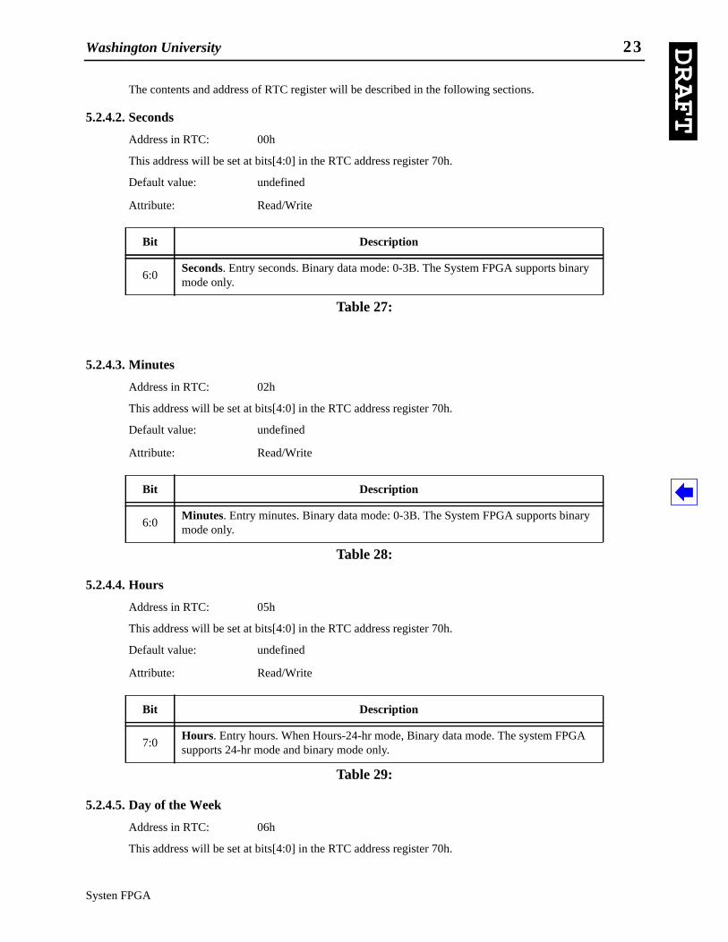
The contents and address of RTC register will be described in the following sections.
5.2.4.2. Seconds
Address in RTC: 00h
This address will be set at bits[4:0] in the RTC address register 70h.
Default value: undefined
Attribute: Read/Write
5.2.4.3. Minutes
Address in RTC: 02h
This address will be set at bits[4:0] in the RTC address register 70h.
Default value: undefined
Attribute: Read/Write
5.2.4.4. Hours
Address in RTC: 05h
This address will be set at bits[4:0] in the RTC address register 70h.
Default value: undefined
Attribute: Read/Write
5.2.4.5. Day of the Week
Address in RTC: 06h
This address will be set at bits[4:0] in the RTC address register 70h.
Bit Description
6:0Seconds. Entry seconds. Binary data mode: 0-3B. The System FPGA supports binarymode only.
Table 27:
Bit Description
6:0Minutes. Entry minutes. Binary data mode: 0-3B. The System FPGA supports binarymode only.
Table 28:
Bit Description
7:0Hours. Entry hours. When Hours-24-hr mode, Binary data mode. The system FPGAsupports 24-hr mode and binary mode only.
Table 29:

24 Applied Research Labratory
spcspec.fm
DRAFT
Default value: undefined
Attribute: Read/Write
5.2.4.6. Day of the Month
Address in RTC: 07h
This address will be set at bits[4:0] in the RTC address register 70h.
Default value: undefined
Attribute: Read/Write
5.2.4.7. Month
Address in RTC: 08h
This address will be set at bits[4:0] in the RTC address register 70h.
Default value: undefined
Attribute: Read/Write
5.2.4.8. Year
Address in RTC: 09h
This address will be set at bits[4:0] in the RTC address register 70h.
Default value: undefined
Attribute: Read/Write
Bit Description
7:0Day of the Week. Binary data mode: 01-07, BCD data mode. The System FPGA sup-ports binary mode only.
Table 30:
Bit Description
7:0Date of the Month. Binary data mode: 01-1F. The System FPGA supports binarymode only.
Table 31:
Bit Description
7:0 Month. Binary data mode: 01-0C. The System FPGA supports binary mode only.
Table 32:

Washington University 25
Systen FPGA
DRAFT
5.2.4.9. RegisterA
Address in RTC: 0Ah
This address will be set at bits[4:0] in the RTC address register 70h.
Default value: 80h
Attribute: Read/Write
5.2.4.10.RegisterB
Address in RTC: 0Bh
This address will be set at bits[4:0] in the RTC address register 70h.
Default value: 06h
Attribute: Read/Write
Bit Description
7:0 Year. Binary data mode: 00-63. The System FPGA supports binary mode only.
Table 33:
Bit Description
7Update In Progress. This bit is hardwired to a 0, which means the update transfer willnot occurbecause the Sysytem FPGA does not support real time clock update function.The System FPGA provides read/write registers only.
6:4 DV[2:0]. These bits are meaningless in the System FPGA.
3:0 RS[3:0]. These bits are meaningless in the System FPGA.
Table 34:
Bit Description
7 SET. This bit is meaningless in the System FPGA.
6 PIE. This bit is meaningless in the System FPGA.
5 AIE. This bit is meaningless in the System FPGA.
4 UIE. This bit is meaningless in the System FPGA.
3 SQWE. This bit is meaningless in the System FPGA.
2 DM. This bit is meaningless in the System FPGA.
1 24/12. This bit is hardwired to 1.
0 Daylight Savings Enable. This bit is meaningless in the System FPGA.
Table 35:

26 Applied Research Labratory
spcspec.fm
DRAFT
5.2.4.11.RegisterC
Address in RTC: 0Ch
This address will be set at bits[4:0] in the RTC address register 70h.
Default value: 00h
Attribute: Read Only
The System FPGA does not support the interrupt function in RTC. Then, whenever this register is read, thevalue is always x00h.
5.2.4.12.RegisterD
Address in RTC: 0Dh
This address will be set at bits[4:0] in the RTC address register 70h.
Default value: 80h
Attribute: Read only
5.2.4.13.CMOS-RAM memory
address 0Eh -- 3Fh
TBD
5.2.5 Emulated BIOS Memory
Address: 0000E0000h-000FFFFFFh
Attribute: Read only
Bit Description
7 Interrupt Request Flag(IRQF). This bit is hardwired to a 0.
6 Periodic Interrupt Flag(PF). This bit is hardwired to a 0.
5 AF. This bit is hardwired to a 0.
4 Update Ended Interrupt Flag(UF). This bit is hardwired to a 0.
3:0 Reserved. These bits are hardwired to 0s.
Table 36:
Bit Description
7 Valid RAM and Time(VRT). This bit is a 1.
6:0 Reserved.
Table 37:

Washington University 27
Systen FPGA
DRAFTEmulated BIOS memory contains FAR JMP to E0000h and codes which copies all of BIOS codes to main
memory(E0000h -- Fxxxxh) and which checks the sanity of writing/reading the main memory address area. TheBIOS codes also include a function that prohibits the access to the Emulated BIOS Memory area after copyingthe BIOS code into main memory. Instead of access to the Emulated BIOS Memory area, the main memory ad-dress space which BIOS codes are copied into can be accessed.
(Jump to the top of BIOS address space)
FFFF FFF0h JMP FAR 0000:E000 (E0 00 E0 00 F0)
(Copy BIOS codes itself into main memory)
000E xxxxh START: PUSH DS
PUSH ES
CLD
MOV AX, 0F000H
MOV DS, AX
MOV SI, 0FFF5H
MOV AX, 0000H
MOV ES, AX
MOV DI, 8000H
MOV CX, 8H
DATE_LP: MOVSB
LOOP DATA_LP
POP ES
POP DS
(Prohibit the access to Emulated BIOS memory directly and provide the access to the shadow memory area)
TBD
(Check the sanity of writing/reading the main memory address space)
TBD
5.2.6 Reset Control Registers
Address: CF9h
Default value: 00h
Attribute: Read/write
Bit Description
7:3 Reserved.
Table 38:

28 Applied Research Labratory
spcspec.fm
DRAFT
5.2.7 Experimental FPGA Configuration Registers (Put off for now)
Experimental FPGA Configuration Registers are used to configure a experimental FPGA on SPC and checkthe configuration status.
5.2.7.1. Configuration Start Register
Address: 0D00h
Default value: 00h
Attribute: Read/write
5.2.7.2. Configuration Data Register
Address: xxxxh
Default value: 0D04h
Attribute: Write Only
2
Reset CPU (RCPU). This bit is used to initiate (transitions from 0 to 1) a hard reset(bit1 in this register is set to 1) or a soft reset to the CPU. During a hard reset, the Sys-tem FPGA asserts CPURST, PCIRST, and RSTDRV. The System FPGA initiates ahard reset when this register is programmed for a hard reset or PWORK is asserted.This bit cannot be read as a 1.
1
System Rest(SRST). This bit is used in conjunction with bit in this register to initiate ahard reset. When SRST=1, the System FPGA initiates a hard reset to the CPU whenbit2 transitions from 0 to 1. When SRST=0, the System FPGA initiates a soft resetwhen bit2 transitions from 0 to 1.
0 Reserved.
Bit Description
7:1 Reserved.
0
Configuration Start. When this bit is set to a 1, the PROGRAM signal pin will beasserted. When this bit is set to a 0, the PROGRAM signal pin will be deasserted. If thisbit is set to a 1 to start the Experimental FPGA configuration, the value must be main-tained until the end of the configuration.
Table 39:
Bit Description
31:0
Configuration Data. The Experimental FPGA configuration data is set to these bits.When Configuration Start bit in Configuration Start Register is set and Configurationdata write status bit is set, the Configuration Data bits can be written into the experi-mental FPGA.
Table 40:
Bit Description
Table 38:

Washington University 29
Systen FPGA
DRAFT
5.2.7.3. Configuration Status Register
Address: sextets
Default value: 0D08h
Attribute: Read/Write Clear
This register indicates some status during the Experimental FPGA configuration. This register is meaninglesswhen Configuration Start bit is not set.
6 System FPGA Functional Description
6.1 Interrupt control
6.1.1 Accommodating interrupt requests
The System FPGA has the function of Programmable Interrupt Controller (PIC). The PIC accommodate thefollowing interrupt requests.
1.A interrupt request from a Programmable Interval Timer (PIT)
2.A interrupt request from a Serial Port (COM1)
3.A interrupt request from a Serial Port (COM2)
4.A interrupt request from APIC.
The interrupt requests from the PIT, COM1, and COM2 are connected to IR0, IR3, adn IR4 of the PIC re-spectively. These connections are same as PC platforms do.
The interrupt request from APIC uses PIRQA signal and the signal is connected to IR5 of the PIC. IR5 isusually connected to the request from Parallel port2 on PC platforms but Parallel port2 is not necessary for SPC.Then, the PIRQA signal could be connected to IR5 on the SPC. The interrupt software driver must hookIRQ5:INT5 entry in Interrupt Vector Table in order to use IRQ5 as APIC's interrupt routine.
Bit Description
15:3 Reserved.
2
Configuration Data Write Status. This bit indicates whether all bits of configurationdata in the Configuration Data Register have been written into the Experimental Sys-tem FPGA. When this bit is set to a 1, the configuration data have been written into theExperimental FPGA. Read only.
1Configuration Error Status. This bit indicates whether any errors occur in the Exper-imental FPGA configuration. When this bit is set to a 0, errors occur in course of theconfiguration. Write clear.
0Configuration Status. This bit indicates status of configuring the Experimental FPGA.When this bit is set to a 0, the configuration is done. When this bit is a 1, the configura-tion is not completed. Read Only.
Table 41:

30 Applied Research Labratory
spcspec.fm
DRAFT
PCI interrupt signal from a experimental FPGA is also run to the System FPGA. However, the implementa-tion of the function in the System FPGA will be put off until the experimental FPGA is implemented on SPC.
6.1.2 IRQ routing
The System FPGA has registers that control the routing of the PIRQ[A:D] signals to the IR inputs of the PIC.The register for PIRQA are hardwired to the value which indicates routing to IRQ5 and other registers are hard-wired to be disabled because PIRQA is connected to IRQ5 as above mentioned and PIRQ[B:D] are not used inSPC. When the experimental FPGA is implemented and the FPGA uses one of PIRQ[B:D], the corredpondingregister will be hardwired to the interrupt to one of IRQs. These registers may be read by NeBSD in interruptconfiguration process.
6.1.3 Interrupt Priority
The PIC in the System FPGA support two priority ordering modes. Other modes which are provided by thepriginal PIC are not supported. This is because of NetBSD does not use other modes. In one mode, IR0 has thehighest prioriy, IR3 has the second, IR4 has the third, and IR5 has the fifth. In another mode, IR3 has the highestprioriy, IR4 has the second, IR5 has the third, and IR0 has the fifth.
6.1.4 Special Mask Mode
NetBSD set special mask mode to PIC if the mode is available. Then, the System FPGA supports SpecialMask Mode. In this mode, when a mask bit is set in OCW1, it inhibits further interrupts at that level and enablesinterrupts from all other levels (lowe as well as higher) that are not masked.
When special mask mode is not set, if an Interrupt Request is acknowledged and an End of Interrupt commanddid not reset its IS bit, the System FPGA whould have inhibited all lower priority requests.
6.1.5 Automatic End of Interrupt mode
If automatic end of interrupt mode is set, a requested ISR bit is reset automatically when the System FPGAreceives the second Interrupt Acknowledge. In non-automatic end of interrupt mode, the requested ISR bit iscleared when the System FPGA receives the specific EOI command.The system FPGA supports automatic endof interrupt mode because NetBSD may require this mode.
6.1.6 Poll command
The System FPGA does not support Poll command since NetBSD does not require this command.
6.1.7 Fully Nested Mode
The System FPGA does not support fully nested mode since NetBSD does not require this mode.
6.1.8 Level Interrupt Mode
The System FPGA will operate in the level interrupt mode. The assertions of interrupt request with One ormore clocks width could be detected as interrupt requests occur.

Washington University 31
Systen FPGA
DRAFT
6.1.9 Interrupt Request Mask
The IMRI (Interrupt Mask Register) stores the bits which disable the interrupt lines to be masked. The IMRoperates on the output of the IRR. Masking og a hihger priority input will not affect the interrupt request lines oflower priority.
6.1.10 Initialization
The PIC in the System FPGA requires the following initialization sequence. In this sequence, some registeres inthe System FPGA are hardwired in advance as mentioned in the following picture.
NetBSD exexutes the PIC initialization according to the following sequence. Refer to NetBSD, ~arch/i386/isa/isa_machdep.c.
isa_defaultirq(){
int i;
/* icu vectors */for (i = 0; i < ICU_LEN; i++)
setgate(&idt[ICU_OFFSET + i], IDTVEC(intr)[i], 0,SDT_SYS386IGT,
SEL_KPL);
/* initialize 8259's */outb(IO_ICU1, 0x11); /* reset; program device, four bytes */outb(IO_ICU1+1, ICU_OFFSET);/* starting at this vector index */outb(IO_ICU1+1, 1 << IRQ_SLAVE); /* slave on line 2 */
#ifdef AUTO_EOI_1outb(IO_ICU1+1, 2 | 1); /* auto EOI, 8086 mode */
#elseoutb(IO_ICU1+1, 1); /* 8086 mode */
#endifoutb(IO_ICU1+1, 0xff); /* leave interrupts masked */outb(IO_ICU1, 0x68); /* special mask mode (if available) */outb(IO_ICU1, 0x0a); /* Read IRR by default. */
#ifdef REORDER_IRQoutb(IO_ICU1, 0xc0 | (3 - 1));/* pri order 3-7, 0-2 (com2 first) */
ICW1(Master 020h, Slave 0A0h)
ICW2(Master 021h, Slave 0A1h)
ICW3(Master 021h, Slave 0A1h)
ICW4(Master 021h, Slave 0A1h)
Ready to Accept Interrupt Request
Hardwired Value
bit0=1:ICW4 needed, bit2=0:cascade mode
MASTER:bit2=1,other bits=0s:IR2 input has a slaveSLAVE:bit[2:0]=1010b
bit0=1:8086 mode, bit3= non buffered mode,bit4=0 Not special fully nested mode

32 Applied Research Labratory
spcspec.fm
DRAFT
#endif
outb(IO_ICU2, 0x11); /* reset; program device, four bytes */outb(IO_ICU2+1, ICU_OFFSET+8);/* staring at this vector index */outb(IO_ICU2+1, IRQ_SLAVE);
#ifdef AUTO_EOI_2outb(IO_ICU2+1, 2 | 1); /* auto EOI, 8086 mode */
#elseoutb(IO_ICU2+1, 1); /* 8086 mode */
#endifoutb(IO_ICU2+1, 0xff); /* leave interrupts masked */outb(IO_ICU2, 0x68); /* special mask mode (if available) */outb(IO_ICU2, 0x0a); /* Read IRR by default. */
}
6.1.11 Master/Slave
The System FPGA has a master PIC function only because all interrupt requests which are accomodatedcould be managed by the master PIC. Hoewver, the System FPGA provides resisters for a slave PIC because Net-BSD try to write and read the resisters in its initialization.
6.1.12 NMI
The System FPGA has NMI status And Control register and NMI Enable and Real-Time Address Register.Bit7 of NMI status And Control register reports the status of PCI SERR. When bit2 of the register is set to 0, theassertion of PCI SERR will cause NMI to CPU.
Bit7 ofNMI Enable and Real-Time Address Register is NMI enable. If the CPU detects NMI, the CPUmustdisable all NMIs by setting the bit7 to a 1 and then enable all NMIs by setting the bit7 to a 0. This will causea new NMI aassertion if there are any pending NMI sources. In the System FPGA, NMI source is only PCI SERR.
6.2 Time Control
6.2.1 Counter0
The PIT (Programmable Interval Timer) in the System FPGA supports counter0 and rate generate mode. Oth-er counters and other modes, which are supported by the original PIT, are not provided by the System FPGA.This is because other counters are for DMA8237 and the speaker but they are not necessary for SPC. In addtion,the counter0 is used for system clock and in the rate generate mode. The couter0 provides binary counter not BCDcounter. The following code is the NetBSD PIT initialization code. Refer to NetBSD, ~arch/i386/isa/isa_machdep.c.
voidstartrtclock(){
int s;
findcpuspeed(); /* use the clock (while it's free)to find the cpu
speed */

Washington University 33
Systen FPGA
DRAFT
/* initialize 8253 clock */outb(TIMER_MODE, TIMER_SEL0|TIMER_RATEGEN|TIMER_16BIT);
/* Correct rounding will buy us a better precision in timekeeping */outb(IO_TIMER1, TIMER_DIV(hz) % 256);outb(IO_TIMER1, TIMER_DIV(hz) / 256);
/* Check diagnostic status */if ((s = mc146818_read(NULL, NVRAM_DIAG)) != 0)/* XXX softc */
printf("RTC BIOS diagnostic error %b\n", (unsigned int) s, NVRAM_DIAG_BITS);
}
6.2.2 Write Operation
For counter0, the Timer Control Word must be written to port 0x40h before the initial count is written. Theinitial count must follow the count format specified in the Timer Control Word (LSB only, MSB only, or LASBand MSB).
6.2.3 Read Operation
There are two possible method for reading the counter, a simple read operation and the Counter latch com-mand. Read Back command, which is provided by 82C54 PIT, is not support by the System FPGA since NetBSDdo not use this operation.
With s simple read operation, to read the counter0, the CLK input of the counter0 must be inhibited. Other-wise, the count may be in the process of changing when it is read, giving an defined result. This operation shouldnot be used because the CLK input can not be inhibited in the FPGA. NetBSD use the Counter Latch Commandwhich is explained in the following paragraph.
The Counter Latch Command, like a Timer Control Words, is written to the Control Word at port 0x43h.Bit[7:4] must be set x”1100” in this case. Bit[7:4] = x”1100” indicates the Counter Latch Command to thecounter0. The selected Counter’s output latch latches the count at the time the Counter Latch Command is re-ceived. This count is held in the latch until it is read by the CPU. The count is the unlatched automatically andthe output latch returns to following the counting element.
6.2.4 Rate Generation
This mode functions like a divide-by-N. Interrupt request from the PIT will initially be low. When the initialcount has decremented to 1, the interrupt request goes high for one CLK pulse. The interrupt request goes lowagain, the Counter reloads the initial count and the process is repeated. This interrupt request run to the IR0 ofinterrupt control.
6.2.5 Clock to Counter0
The clock to counter0 is generated from dividing 33 MHz clock by 27 or 28. In the PC plarforms,1.19318MHz clock is used as the clock to counter0. In the System FPGA, the divide clock is used to synchronizethe all circuits by the 33MHz clock to be easy to implement. The following picture explain the divided clock waveform. With this scheme, couter0 is faster 0.87 ns 3 1.193182MHz clocks or 0.015ns per 105 1.193182MHzclocks.

34 Applied Research Labratory
spcspec.fm
DRAFT
Cycle Devided-N Gap
0 27/28/28 0.87ns
1 27/28/28 0.87ns
2 27/28/28 0.87ns
....................
33 27/28/28 0.87ns
34 27/27/28 0.015ns. This cycle scrinks the gap.
6.3 Real Time Clock control
6.3.1 No Real Time Clock function
Registers of Real Time Clock(RTC), which a microprocessor can read/write, are supported by the SysytemFPGA. However, thw System FPGA does not provide the calendar function of the original RTC function.
NetBSD read the calendar in the RTC in initialization sequence. However, NetBSD does not use RTC to up-date sec, minutes, hour, day, month, and year in the calendar function during run-time. It use the interupt fromthe PIT to update the calendar of NetBSD. On SPC, a boot loader writes initial value of calendar to registers ofRTC and then NetBSD read the value in initialization. This could make the System FPGA implimentation easier.The second and minitue of calendar will be slow but it is negligible in experiment situations.
0 1 25 26 0 1 26 27 0 125
divided by 27 divided by 28
26 27 0 125
divided by 28
33MHz clock
divided clock
1.193182MHzclock
818.18ns
838.095ns
848.48ns 848.48ns
838.095ns 838.095ns 0.87ns
dividedby 27
dividedby 28
dividedby 28
Cycle 0
dividedby 27
dividedby 28
dividedby 28
Cycle 33
dividedby 27
dividedby 27
dividedby 28
Cycle 34
0.015ns

Washington University 35
Systen FPGA
DRAFT
6.3.2 NVRAM area
The system FPGA provide the following register in NVRAM area which NetBSD may read.
Offset Description
0Eh diagnosis status. The value is hardwired to
RTC power supply is OK, Checksum is OK, Configuration is OK, Evaluated memory size is OK,
Harddisk is conroller or drive initialization failed, and time is OK.
0Fh Shutdown Staus. Default: 00h=normal system reset. This register is possible to read and write.
10h type of Floppy drives. Hardwired to x”00” to indicate first and second floppy drive is not installed.
12h type of Hard disk drives. Hardwired to x”00” to indicate first and second Hard disk drive is not
installed.
14h Device type. The value is hardwired to
floppy drive is not installed, coprocessor 80x87 is not installed, and graphic adapter is ???.
15h base memory size(low byte). The value is set based on external pins to indicate Main memory size.
16h base memory size(high byte). The value is set based on external pins to indicate Main memory size.
17h extended memory size(low byte).
The value is set based on external pins to indicate Main memory size.
18h extended memory size(high byte).
The value is set based on external pins to indicate Main memory size.
32h Century. This register will be hardwired to 1997.
6.4 Reset Control
6.4.1 Hard Reset
Hard reset will be generated when bit1 in Reset Control Register is a 1 and bit2 translates a 0 to a 1 or whenPWORK signal is asserted. Hard reset assert three external signals (CPURST and PCIRST#) and resets the cur-rent state in the System FPGA.
The assertion of PWORK indicates to the System FPGA that power and PCICLK have been stable for at least1ms. PCIRST# an CPURST are driven inactive a minimum of 1ms after PWORK is driven active. PCIRST# andCPURST are driven active for a minimum of 1ms when initiated through the RC register.
Pentium requires;
CPURST for a minimum of 15 clk cycles
PCI bus specification requires;
The RST# signal line is asserted a minimum of 1ms.
The CLK signal line has been oscillating a minimum of 100microseconds.
Voltage level outlined in table 11-1 have remained above the minimum leves(PWR_GOOD# asserted) forabout 100 ms.

36 Applied Research Labratory
spcspec.fm
DRAFT
6.4.2 Soft Reset
Soft reset will occur at the time bit2 in Reset Control Register tansits 0 to 1 and bit1 is equal to 0. Soft resetasserts INIT signal to microprocessor for a minimum two 66MHz clock cycles.
6.5 Emulated BIOS
Pentium read a instruction at FFFF FFF0h in BIOS memory space in the System FPGA. The instruction isFAR JMP to the top of the instruction sets which ececutes Main Memory Check and Loop to wait for OS down-load. The FAR JMP and the instruction sets are read-only register in the Sysytem FPGA.
Memory Check codes write a data to a address in main memory space and compare. If the written data andthe read data are same, the succeeding address is testified. If all addresses in main memory are testified and anyerror have not been found, the codes goes into Loop process. Some external pins should be set to indicate mainmemory size to the System FPGA before the System FPGA is configured.
During of loop execution, OS and application software are downloaded through APIC. Microprocessor willbe execute loop process that read and check a value of a register in the System FPGA until the value transits 0 to 1.
Other functions which are provided by the original BIOS are executed by the down-loaded boot-loader.
6.6 UART
6.7 Experimental FPGA configuration control (put off for now)
6.7.1 Overview of FPGA configuration
The basic operation of the FPGA configuration schemes is composed of the following stages.
1. The device configuration memory is cleared.
2. Configuration data is clocked into the device.
3. After a successful download, the FPGA asserts its DONE signal.
6.7.2 Slave Serial Mode
The System FPGA use the Slave Serial mode to configure the experimental FPGA on SPC. The Slave Serialmode requires only three active signals.
1. DIN, the data in pin.
2. Configuration Clock, CCLK.
3. PROGRAM which has been asserted during the configuration.
6.7.3 Configuration Sequence through the System FPGA
1: Set bit1 in Configuration Start Register in order to assert PROGRAM signal pin.
2: Read bit2 in Configuration Status Register. If the value is a 0, it is possible to write a
configuration data to Configuration Data Register.
3: If a configuration data is written to bit[7:0] in the System FPGA, the System FPGA output
the data bit by bit with Configuration Clock. During this output sequence, bit2 in Configuration Data

Washington University 37
Systen FPGA
DRAFT
Write Status is set 1 automatically. If all bit have been sent to the experimental FPGA, Configuration
Clock get non-activated and bit2 in Configuration Data Write Status is set 1.
4: Repeat 2 and 3 until microprocessor write all of configuration data into the Configuration Data
Register. If the configuration has been finished, the experimental FPGA asserts DONE signal.
Assertion of the DONE signal set bit0 Configuration Status Register to 1.
5: Lock signal to the experimental FPGA is asserted. The signal will have been asserted in order to
prevent further access.

38 Applied Research Labratory
spcspec.fm
DRAFT
7 System FPGA Implementation
7.1 Detailed BLock Diagram
consumerreadyconsumeraddrconsumertypeiostrobe
datain(31:0)
consumerdatareturn(31:0)consumerreturnstrobe
irdy_ltrdy_lstop_l
pciclkmad(31:0)cbe_l(3:0)frame_l
devesel_llock_lperr_lserr_lidselpar
pcislave registermanager interrupt_control
data_from_pic(7:0)
addr_to_pic
data_to_pic(7:0) apic_int_l
intr
pic_data_dir
clkinresetin_l
clkinresetin_l
pit_selectaddr_to_pit
pit_data_dir
data_to_pit(7:0)
data_from_pit(7:0)
pitint
rtc_data_dirdata_from_rtc(7:0)
data_from_rtc(7:0)
addr_to_rtc(7:0)
real_time_control
resetin_lclkin
resetin_lclkin
addr_bios(15:0)bios_read
data_from_bios(31:0)
bios_ctl
pworkpcirstcpurst
resetin_l
resetin_l
addr_to_config(1:0)data_to_config(7:0)
ef_cclkef_program
ef_lockef_done
config_data_dirdata_from_config(7:0)
ef_init
ef_din
reset_ctl
config_ctl
resetin_lclkin
init
nmi_select
data_to_nmi(7:0)
nmi_data_dir
data_from_nmi(7:0)
pic_slave_selectlpic_master_select
rtc_select
data_to_reset(7:0)reset_data_dir
data_from_reset(7:0)
memstrobeiackstrobe
nmi
ef_int_l
timer_control
uart_control
uart1_int
uart2_int
pirqain(7:0)pirqbin(7:0)pirqcin(7:0)pirqdin(7:0)
clkin

Washington University 39
Systen FPGA
DRAFT
7.2 PCI Slave
7.3 Register Manager
7.3.1 Decode
The following list indicates the address which the decoder decodes to initiate the read/write cycle.
When the register manager detects the assertion of IOstrobe, it decodes the received address as a address toI/O space. On the other hands, when MEMstrobe is asserted, the register manager decodes the address as memoryaddress.
In order to read/write a data from/to a register in RTC, first, the address register at 070h should be set to aaccessed address, then, the data register at 071h should be accessed. When the data register is accessed, the reg-ister manager send the address which is set at 070h previously, as a address to RTC. When the address registeris accessed to write a data, the register manager keeps the data and does not assert signals to RTC. However, bit7of the address register is located in interrupt_control because this register is shared with NMI and RTC.
I/O, Memory Address Function block to select
020h (I/O) Interrupt_Control:Master PIC
021h (I/O) Interrupt_Control:Master PIC
0A0h (I/O) Interrupt_Ccontrol:Slave PIC
0A1h (I/O) Interrupt_Control:SlavePIC
061h (I/O) Interrupt_Control:NMI status and control
070h (I/O)Interrupt_Control( shared with Address register of RTC):CMOS RAM address and NMI enalbe
040h (I/O) Timer_Control:Counter0
043h (I/O) Timer_Control:Timer Control Register
070h (I/O)Real_Time_Control:( shared with NMI enable register):CMOS RAM address and NMI enalbe
071h (I/O) Real_Time_Control:CMOS RAM data
03F8h -- 03FEh (I/O) UART1 (This will be connected to external bus.)
02F8h -- 02FEh (I/O) UART2 (This will be connected to external bus.)
0CF9h (I/O) Rest_Control
0D00h -- 0D08h Ex_FPGA_Config_Control
FFFEFFFFh-- FFFEFFFFh,000EFFFFh-- 000EFFFFh(memory)
Bios_Control
Table 42:

40 Applied Research Labratory
spcspec.fm
DRAFT
The adress and the data are transfered to the external bus at the time UART1/2 is accessed.
7.3.2 Read/Write Operation to other internal Function Blocks
The register manager expects non-wait access to the registers in other internal function blocks. The followingfigure notes the read/write access to other internal function blocks.
7.3.3 Read/Write Operation to external Function Block (UART)
The following figure notes the read/write access to UART which is located at outside of this FPGA.
Address
Select
Direction(1=write,0=read)
Write Opearation
Data_Out
Read Opearation
(to other function block)
(to other function block)
(to other function block)
(to other function block)
(from other function block)
33MHz clock
Data_IN
Decode
Grab a data
Decode
Return Data(to PCI Slave stuff)
Decode
1 2 31 2

Washington University 41
Systen FPGA
DRAFT
7.3.4 PIRQ[A:D] Route Register
The register manager has PIRQ[A:D] route registers. This registers are hardwired the output of these registersare run to PCI-SLAVE stuff. These registers address is decoded as a address in PCI Configuration space.
33MHz clock
Write Operation Read Opearation
grab a data
decode
Chip Select
Output fromRegistermanager
Channel Selectselect CH1
Addressinvalid valid invalid
Datainvalid valid invalid
Write
Chip Select
Output to UART-IC(external signals)
Channel Select
Address
Data
Write
1 2 3 4 5 6 7 8
Write Enable
select CH1
invalid valid invalid
invalid valid invalid
Read
Read Enable
decode
invalid valid invalid
invalid valid invalid
select CH1
invalid valid invalid
valid invalid
1 2 3 4 5 6 7 8
Data from UART
Read

42 Applied Research Labratory
spcspec.fm
DRAFT
7.4 Interrupt Control
7.4.1 Interrupt Acknowledge Sequence
7.4.2 Blocking Interrupt Request
In the normal mode, if an interrupt request is acknowledged and an End of Interrupt command did not resetits IS bit (i.e., while executing a service routine), the Sysytem FPGA would have inhibited all lower prority re-quests.
In the Special Mask Mode, when a msk bit is set in OCW1, it inhibits further interrupt at that level and enablesinterrupts from all other levels (lower as well as higher) that are not masked. Any interrupts may be selectivelyenabled by loading the mask register.
Between first INTA and second INTA, the status of IRR (Interrupt Request Register ) is freezed (latched).Then, interrupt requests are blocked and are not stored in IRR.
Between second INTA and EOI command, lower interupt requests than the processed interrupt request arestored in IRR but could not request a interrupt service routine (assertion of INTR) even if the according IMR bitis no set int the normal mode. Interrupt requests in Special Mask Mode could be stored in IRR and request a in-terrupt service routine (assertion of INTR) if the according IMR bit is not set.
INTR
INTA_command
Freeze_IRR(internal signal)
Interrupt Prioriy Resolution
Data_Out
(from other function block)
(to CPU)
(from CPU(via registermanager)
(to register manager)
33MHz clock
Interrupt Request
Set ISRBlock other IRs
Unblock other IR
Interrupt Vector Address
EOI_command(from CPU(via registermanager)
Address
Select
Direction(1=write,0=read)
(from register manager)
(from register manager)
(from register manager)
(from register manager)
Data_IN
EOI(Bit(7:5) of OCW2=001b)
(Latch the state of IRR)

Washington University 43
Systen FPGA
DRAFT
7.4.3 Ininitialization Sequence
The System FPGA requires the initial sequence which is described in 5.1.10. The state in the Sysytem FPGAtransit to the succeding state at the time each ICW is received. After reset, the Sysytem FPGA goes to the statewhich is waiting for writeing ICW1 immedeatly. After writeing ICW1, goes to the state which is waiting forICW2. Finally, initialization is completed after ICW4 is written.
7.4.4 NMI
7.5 Timer Control
7.5.1 Internal Block Diagram
7.5.2 Control Word Register
The System FPGA supports counter0 and mode2 (rate generator) only. The according registers are hardwiredto set this mode. Control Word Register and Read/Write logic has control states which are Counter Latch Com-mand state, Read/Write LSB only state, Read/Write MSB only state, and Read/Write LSB first, then MSB state.These states are set by writing a data to Control Register.
In Counter Latch Command state, the System FPGA latches the value of counter0 at Output Latch, and ex-pects CPU reads LSB first and then MSB. After reading LSB and MSB, these value are unlatched respectively.
In Read/Write LSB only state, Read/Write MSB only state, and Read/Write LSB first, then MSB state, thevalue of counter0 is not latched. CPU reads the output from Output Latch according to the state which is set intoControl Word register.
7.5.3 Counter Enable
Writing the inial counter data to Couner Register enables counter0 operation. After reset, counter0 is dsable.After set of Counter Register, counter0 operation is started. On the other hand, 33MHz divider is always enabledand is not enable by setting a register.
7.5.4 Counter0 Operation with Mode2 (Rate Generator)
This mode functions like a divide-by-N counter. Interupt request to interrupt control is initially low. Whenthe initial count has decremented to 1. The interrupt request goes high 1 33MHz clock. The interrupt request then
33MHz clock divider
counter0
CounterRegister
OutputLatch
Register,Control Word
Read/WriteLogicaddress, data,
etc
enable33MHz clock
emulated1.19318MHzclock
latch

44 Applied Research Labratory
spcspec.fm
DRAFT
goes low again, the counter0 reloads the initial count and the process is repeated. For an initail count of M, thesequence repeats every M clk cycles. After writing a Timer Control Word and initial count, the counter0 will beloaded on the next clk pulse.
The following picture describes the mode 2 operation.
7.5.5 33MHz clock divider
The operation of 33MHz clock is described in 5.2.5. This divider is always enabled to generate the1.19318MHz clock. This divider has three counters in it. One is the counter which divide 33MHz clk by 27 or28. Other two counters are used for deciding whether 33MHz clk should be divided by 27 or 28.
Assumed Cij is the cycle number which indicate 33MHz clk should be divided by 27 or 28, and i is one of(0,1,2) and j is one of (0,1,2,...,33,34). Cij is incremented and repeated like C0.0, C0.1, C0.2, C1.0, C1.1, C1.2,...,C34.0,C34.1, C34.2, C0.0, C0.1, C0.2,.... The other two counters are for representing i and j. In the cycle: Cij with j=0 andCij with j=2 and i=34, 33MHz clk is divided by 27. In other cycles, 33MHz clk is divided by 28.
7.6 Real_Time_Clock_Control
As described in 5.3, real_time_clock_control comprises a bunch of registers. Some registers are hardwired andsome registers are read/write enabled.
7.7 Emulated BIOS Control
Emulated bios control comprises an array of read only registers.
7.8 Reset_Control
7.8.1 Internal Block
counter0 value
pint_int(Interrupt Request to interrupt control)
1.19318MHz
Timer Control Word
counter0 disable
N
Set Timer Control Word
clock
Operation
Set LSB Set MSB
N N N N N M M-1 M-2 M-3 3 2 1 M M-1 M-2
counter0 enabled

Washington University 45
Systen FPGA
DRAFT
7.8.2 Hardware Reset
Hard reset will be generated when bit1 in Reset Control Register is a 1 and bit2 translates a 0 to a 1 or whenPWORK signal is asserted. Hard reset assert three external signals (CPURST and PCIRST#) and resets the cur-rent state in the System FPGA.
The following figures describes the time-chart of reset sequence. Internal Reset signal, CPURST, and PCIR-ST are asserted when PWORK is negated or hard reset trigger signal is asserted. The hard reset trigger signal isasserted when bit1 in Reset Control Register is a 1 and bit2 translates a 0 to a 1. Then, Internal Reset signal,CPURST, and PCIRST will be asserted for 1msec (33K 33MHz Clock pulses). Hard reset generator has 16bitcounter. The counter starts to count and internal reset signal, CPURST, and PCIRST are asserted after PWORKis asserted. When the The count is incremented to 33K, couting is stopped and internal reset signal, CPURST,and PCIRST are deasserted.
Hard ResetGeneratorRegister,
Read/WriteLogicaddress, data,
etc
Hard Reset PWORKTrigger
CPURST
PCIRST
Internal Reset
Soft ResetGenerator
Soft ResetTrigger INIT
CPURST
33MHz
PWORK
clock
PCIRST
InternalReset
1msec (33K 33MHz clk)

46 Applied Research Labratory
spcspec.fm
DRAFT
7.8.3 Soft Rest
Soft reset will be generated when bit1 in Reset Control Register is a 0 and bit2 translates a 0 to a 1.
The following figures describes the time-chart of reset sequence. INIT is asserted when soft reset trigger sig-nal is asserted. The soft reset trigger signal is asserted when bit1 in Reset Control Register is a 0 and bit2 trans-lates a 0 to a 1. INIT will be asserted for a 2 clock.
7.9 EXP-FPGA Config_Control (put off now)
CPURST
33MHz
Hard Reset
clock
PCIRST
InternalReset
1msec (33K 33MHz clk)Trigger(by set of RC register)
33MHz
Soft Reset
clock
INIT
2 33MHz clkTrigger(by set of RC register)

Washington University 47
Systen FPGA
DRAFT
8 Development Board Design
XilinxFPGA
RibbonConnector
PCI Proto Board
HostSystem
APIC
RibbonConnector
APIC Board
PCI Bus
BidirectionalUtopia Ports
FPGAMini-network Intel Embedded
Module
DRAMConnector
SystemFPGA
ExperimetationFPGA
SerialEPROM
Xchecker
Side BandSignals
Development Board
8