
© Copyright 2012 Xilinx
SP605 MIG Design Creation
March 2012
XTP060

© Copyright 2012 Xilinx, Inc. All Rights Reserved. XILINX, the Xilinx logo, the Brand Window and other designated brands included herein are trademarks of Xilinx, Inc. All other trademarks are the property of their respective owners. NOTICE OF DISCLAIMER: The information disclosed to you hereunder (the “Information”) is provided “AS-IS” with no warranty of any kind, express or implied. Xilinx does not assume any liability arising from your use of the Information. You are responsible for obtaining any rights you may require for your use of this Information. Xilinx reserves the right to make changes, at any time, to the Information without notice and at its sole discretion. Xilinx assumes no obligation to correct any errors contained in the Information or to advise you of any corrections or updates. Xilinx expressly disclaims any liability in connection with technical support or assistance that may be provided to you in connection with the Information. XILINX MAKES NO OTHER WARRANTIES, WHETHER EXPRESS, IMPLIED, OR STATUTORY, REGARDING THE INFORMATION, INCLUDING ANY WARRANTIES OF MERCHANTABILITY, FITNESS FOR A PARTICULAR PURPOSE, OR NONINFRINGEMENT OF THIRD-PARTY RIGHTS.
Revision History
Date Version Description 03/16/12 13.4 Up-rev to MIG 3.91.
10/26/11 13.3 Up-rev to MIG 3.9.
07/06/11 13.2 Up-rev to MIG 3.8. Applied AR41721.
03/01/11 13.1 ARs Fixed in MIG 3.7: AR36741 – Traffic Generator Data Pattern cannot be modified
12/21/10 12.4 ARs Present in MIG 3.61: AR36741 – Traffic Generator Data Pattern cannot be modified
10/05/10 12.3 ARs Present in MIG 3.6: AR36741 – Traffic Generator Data Pattern cannot be modified
07/23/10 12.2 ARs Fixed in MIG 3.5: AR35499 – Traffic Generator module update AR35250 – XST Project file change ARs Added in MIG 3.5: AR36741 – Traffic Generator Data Pattern cannot be modified

Overview
Spartan-6 Memory Controller Block Xilinx SP605 Board Software Requirements SP605 Setup Generate MIG Core Modifications to Example Design Compile Example Design ChipScope Pro Setup Run MIG References
Note: This presentation applies to the SP605
Spartan-6 Memory Controller Block
Dedicated Memory Controller Blocks (MCB) for Simplified DRAM interfaces – Up to 4 MCB cores in a single Spartan-6 device – Embedded controller and physical (PHY) interface – Supports 4-bit, 8-bit, or 16-bit single component memory – Memory densities up to 4 Gbit
Performance up to 667 Mb/s (333 MHz double data rate) Configurable dedicated Multi-port user interface to FPGA logic
– 1 to 6 ports per MCB depending on configuration – Internal 32-, 64-, or 128-bit data bus options
Note: Presentation applies to the SP605

MCB Block Diagram
Simple User Interface abstracts away complexity of memory transactions MIG / EDK wrapper delivers complete interface solution
– Internal block assembly and signal connectivity is made transparent to the user
Note: Presentation applies to the SP605

Memory Controller Block Startup
Automatic memory configuration and controller calibration
Note: Presentation applies to the SP605

Xilinx SP605 Board
Note: Presentation applies to the SP605
ISE Software Requirement
Xilinx ISE 13.4 software
Note: Presentation applies to the SP605
ChipScope Pro Software Requirement
Xilinx ChipScope Pro 13.4 software
Note: Presentation applies to the SP605
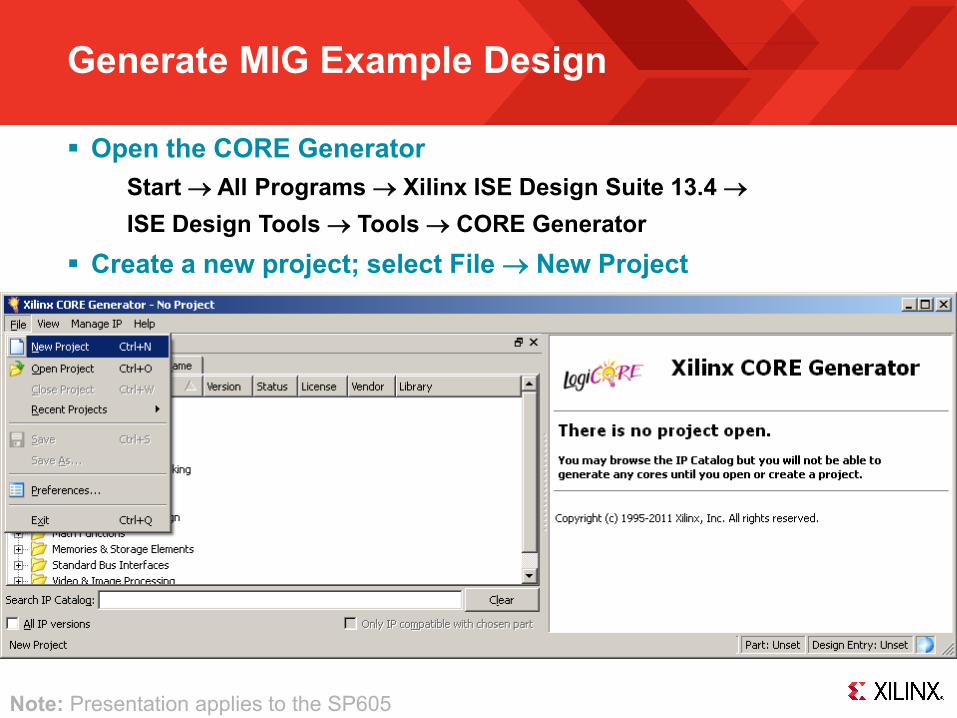
Generate MIG Example Design
Open the CORE Generator Start → All Programs → Xilinx ISE Design Suite 13.4 → ISE Design Tools → Tools → CORE Generator
Create a new project; select File → New Project
Note: Presentation applies to the SP605

Generate MIG Example Design
Create a project directory: sp605_mig_design
Note: Presentation applies to the SP605
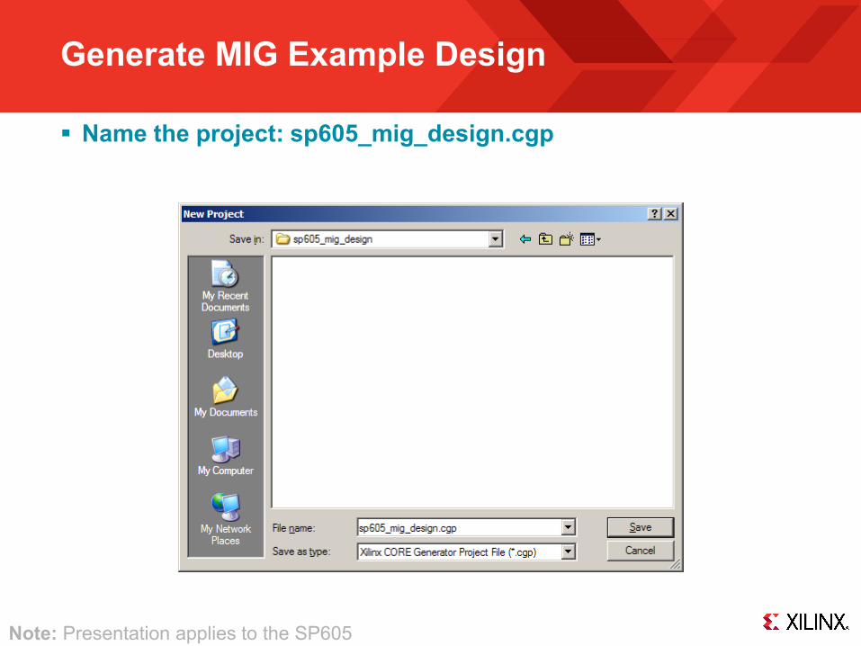
Generate MIG Example Design
Name the project: sp605_mig_design.cgp
Note: Presentation applies to the SP605
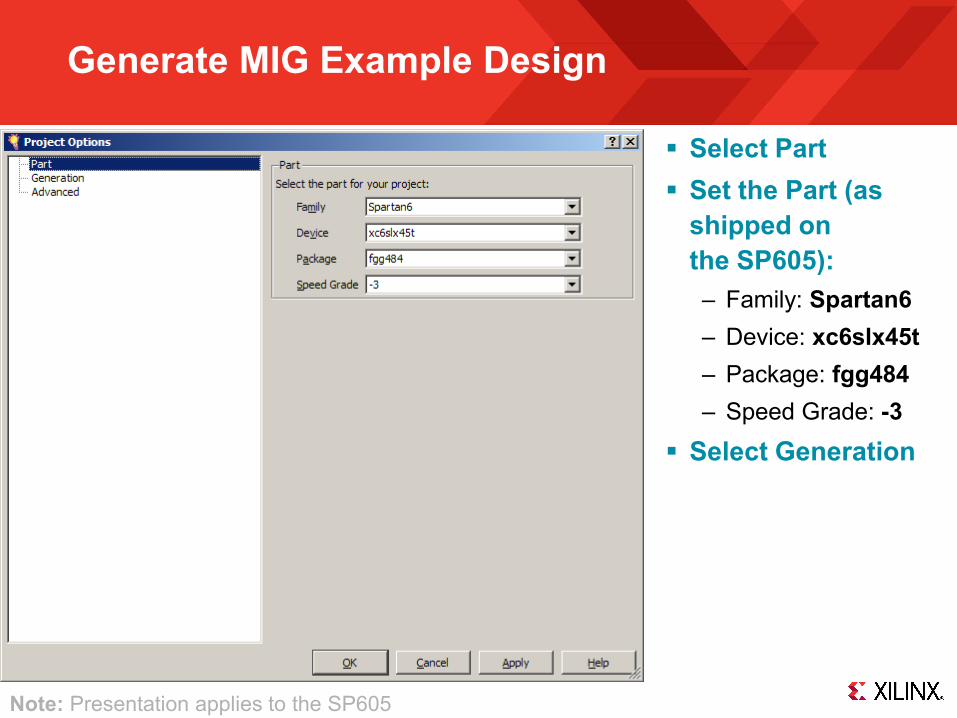
Generate MIG Example Design
Select Part Set the Part (as
shipped on the SP605): – Family: Spartan6 – Device: xc6slx45t – Package: fgg484 – Speed Grade: -3
Select Generation
Note: Presentation applies to the SP605

Generate MIG Example Design
Under Generation – Set the Design Entry
to Verilog
Click OK
Note: Presentation applies to the SP605

Generate MIG Example Design
Right click on MIG Version 3.91 – Select Customize and Generate
Note: Presentation applies to the SP605

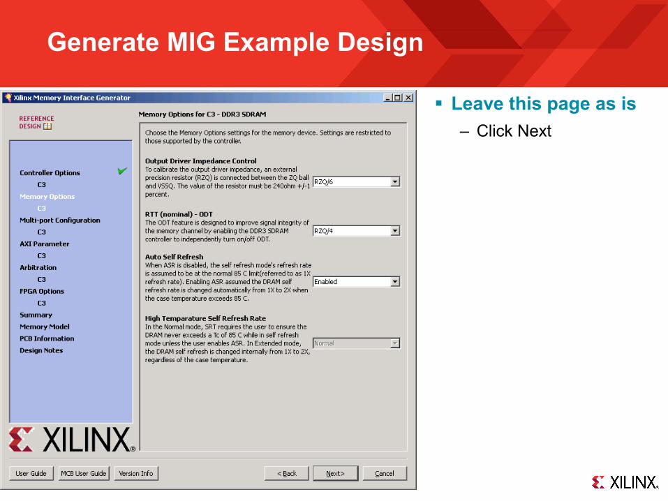
Generate MIG Example Design
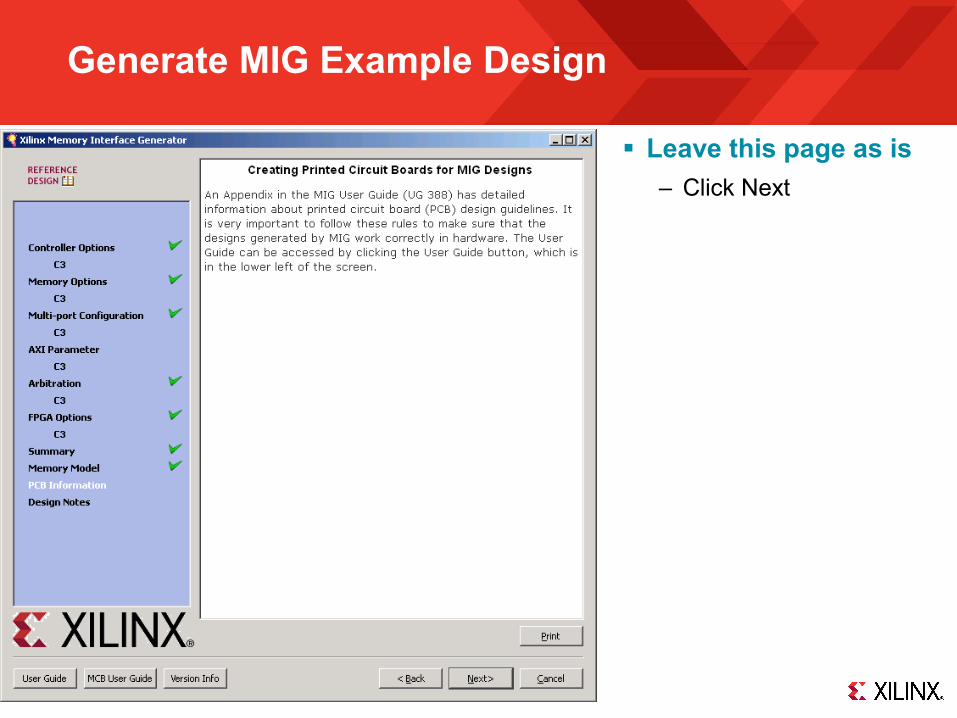
Leave this page as is – Click Next

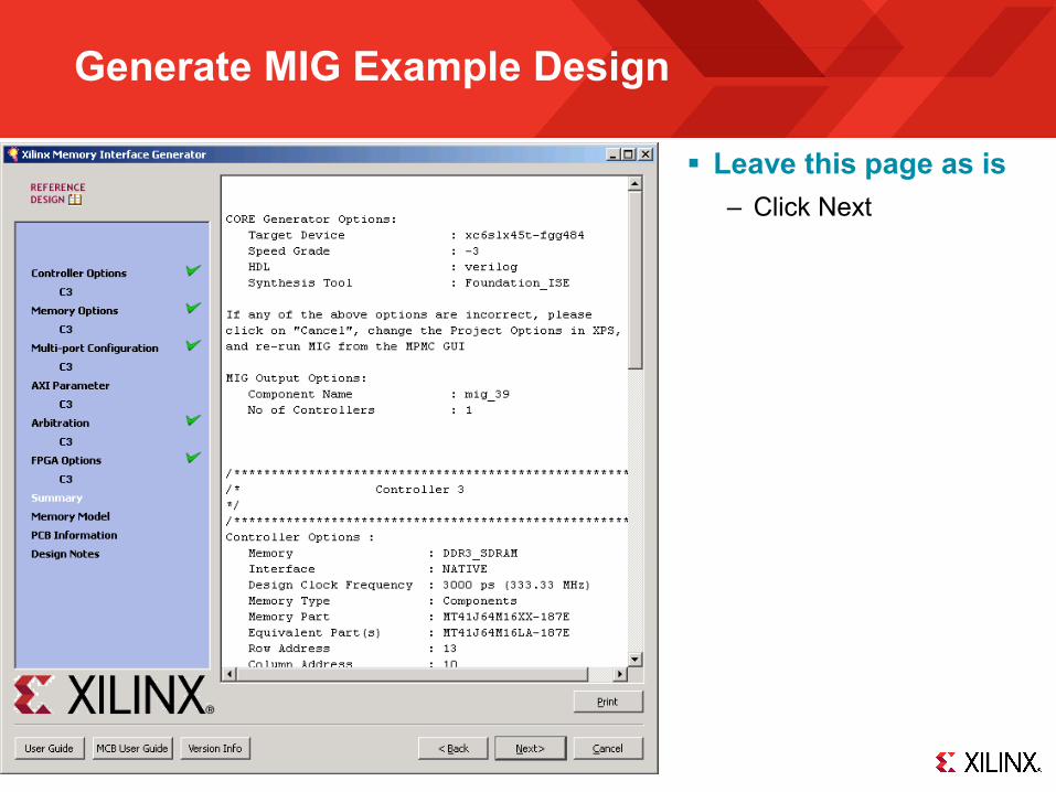
Generate MIG Example Design
Leave this page as is – Click Next

Generate MIG Example Design
Leave this page as is – Click Next

Generate MIG Example Design
For the Bank 3 Middle MCB, select Memory Type – DDR3 SDRAM – Click Next

Generate MIG Example Design
Set the Frequency to 333.33 MHz (3000 ps) – DDR3 Performance
documented in the Spartan-6 FPGA Data Sheet
Set the Memory part to MT41J64M16XX-187E – Click Next
Generate MIG Example Design
Leave this page as is – Click Next

Generate MIG Example Design
Select – One 128-bit bi-
directional Port – Click Next

Generate MIG Example Design
Leave this page as is – Click Next

Generate MIG Example Design
Select Calibrated Input Termination
Set RZQ pin location – K7
Set ZIO pin location – M7
Set Debug Signals – Enable – Click Next
Generate MIG Example Design
Leave this page as is – Click Next

Generate MIG Example Design
Accept Simulation license, if desired – Otherwise, Decline
license – Click Next
Generate MIG Example Design
Leave this page as is – Click Next

Generate MIG Example Design
Click Generate

Generate MIG Example Design
After the MIG core finishes generating, click Close on the Datasheet window
Note: Presentation applies to the SP605
Generate MIG Example Design
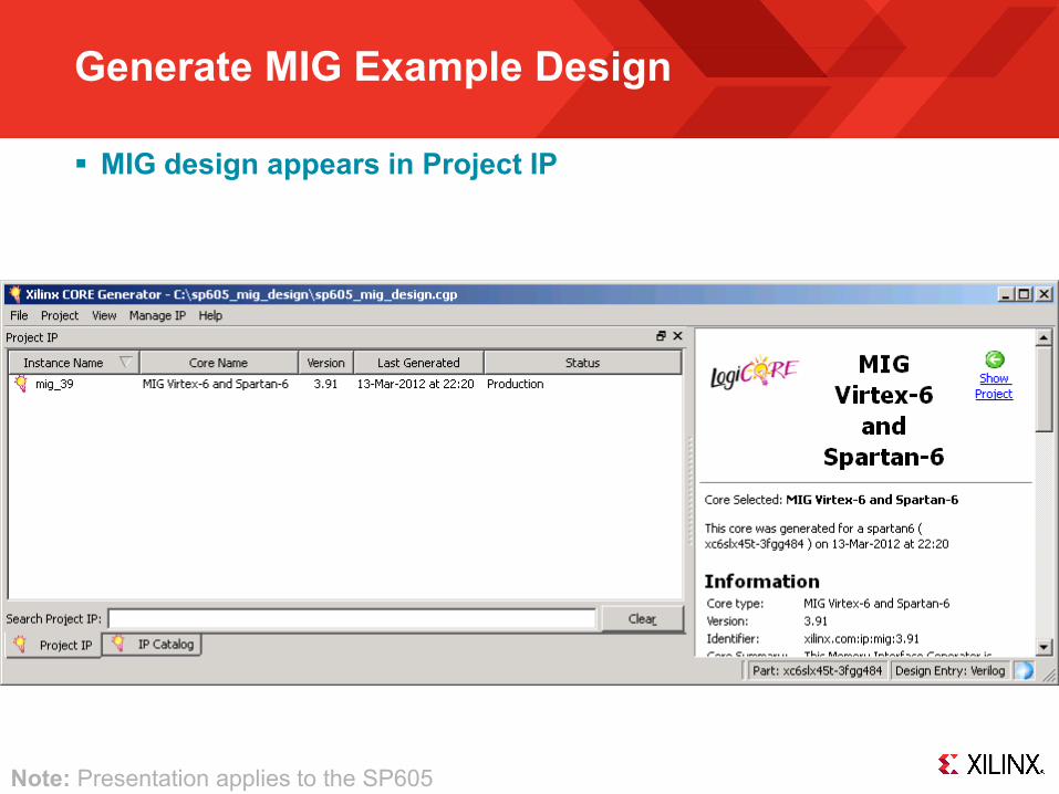
MIG design appears in Project IP
Note: Presentation applies to the SP605

Modifications to Example Design
RDF0029 includes – ChipScope Project File, UCF, Verilog Files, and pre-built Example Design
files – Available through http://www.xilinx.com/sp605
Modifications to RTL Files for SP605 Example Design – Added GPIO outputs for visual status indicators with heartbeat clock
• GPIO LED 3 = Calibration done • GPIO LED 2 = PLL locked • GPIO LED 1 = Error • GPIO LED 0 = Heartbeat (blinking)
– Change CLKFBOUT_MULT to generate proper clocks: • MCB block runs at 667 MHz • Traffic Generator runs at 83.33 MHz • Soft calibration clock runs at 83.33 MHz
Note: Presentation applies to the SP605

Modifications to Example Design
Updates to UCF file specifically required for SP605 board: – Changed LOC of 200MHz differential sys_clk inputs – Changed LOC of sys_rst_n input to SP605 CPU_RESET switch – Added LOC for GPIO LED signals (2.5V bank voltage) – Increase sys_clk_ibufg period constraint from 3ns to 5ns
Note: Presentation applies to the SP605
Modifications to Example Design
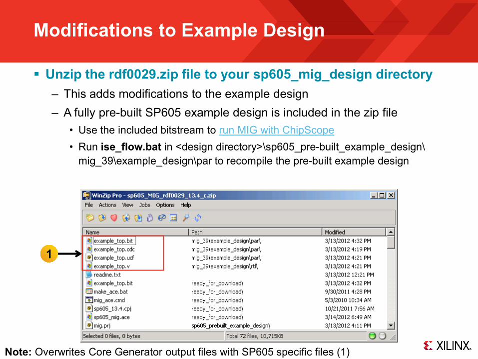
Unzip the rdf0029.zip file to your sp605_mig_design directory – This adds modifications to the example design – A fully pre-built SP605 example design is included in the zip file
• Use the included bitstream to run MIG with ChipScope • Run ise_flow.bat in <design directory>\sp605_pre-built_example_design\
mig_39\example_design\par to recompile the pre-built example design
Note: Overwrites Core Generator output files with SP605 specific files (1)
1

Compile Example Design
Start a ISE Design Suite Command Prompt and enter these commands:
cd C:\sp605_mig_design\mig_39\example_design\par ise_flow.bat
Note: Presentation applies to the SP605

Setup for the SP605 MIG Designs
Connect a USB Type-A to Mini-B cable to the USB JTAG connector on the SP605 board – Connect this cable
to your PC

Running the SP605 MIG Design
Open ChipScope Pro and click on the Open Cable Button (1) Click OK (2)
1
2
Note: Presentation applies to the SP605

Running the SP605 MIG Design
Select Device → DEV:1 MyDevice1 (XC6SLX45T) → Configure… Select <Design Path>\mig_39\example_design\par\example_top.bit
Note: Presentation applies to the SP605

ChipScope Pro Setup
Select File → Open Project… Select <Design Path>\ready_for_download\sp605_13.4.cpj
Note: Presentation applies to the SP605

Run MIG Example Design
Click on Trigger Setup to view trigger settings The error bit value should be set to 1
Note: Presentation applies to the SP605

Run MIG Example Design
Click on Waveform; click the Arm Trigger button (1) Detection of an error will cause ChipScope Pro to trigger
Note: Presentation applies to the SP605
1

Run MIG Example Design
The Example Design should run error free (no trigger on error) To force a trigger, click the T! button (1)
Note: Presentation applies to the SP605
1

Adjust Data Pattern using VIO Console
Select VIO Console Set TrafficGen_VIO_Enable to 1
Note: Presentation applies to the SP605
Adjust Data Pattern using VIO Console
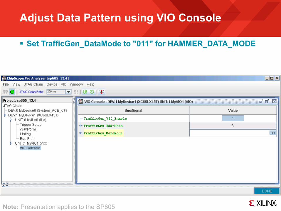
Set TrafficGen_DataMode to "011" for HAMMER_DATA_MODE
Note: Presentation applies to the SP605

Adjust Data Pattern using VIO Console
Press and release the CPU RESET switch, SW6, after each VIO change

Adjust Data Pattern using VIO Console
Click on Waveform; click the Arm Trigger button (1) Force a trigger by clicking the T! button (2)
Note: Presentation applies to the SP605
1 2

Adjust Data Pattern using VIO Console
Hammer Data Mode – 16 bit DQ data bus changes all bits on each cycle, “hammering” the bus – Read data compared with ‘expected’ data and error generated on mismatch
Note: Presentation applies to the SP605

Adjust Data Pattern using VIO Console
Set TrafficGen_DataMode to "101" for WALKING1_DATA_MODE Push CPU Reset, click Arm Trigger button, click T! button
Note: Presentation applies to the SP605

Adjust Data Pattern using VIO Console
Walking 1s Data Mode
Note: Presentation applies to the SP605

Adjust Data Pattern using VIO Console
See UG388 for more details on the available data patterns – ADDR_DATA_MODE = 3'b010;
– HAMMER_DATA_MODE = 3'b011;
– NEIGHBOR_DATA_MODE = 3'b100;
– WALKING1_DATA_MODE = 3'b101;
– WALKING0_DATA_MODE = 3'b110;
– PRBS_DATA_MODE = 3'b111;
Note: Presentation applies to the SP605
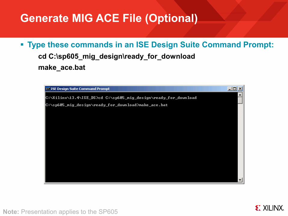
Generate MIG ACE File (Optional)
Type these commands in an ISE Design Suite Command Prompt: cd C:\sp605_mig_design\ready_for_download make_ace.bat
Note: Presentation applies to the SP605

References

References
Spartan-6 – Spartan-6 FPGA Memory Controller – UG388
http://www.xilinx.com/support/documentation/user_guides/ug388.pdf – Spartan-6 FPGA Memory Interface Solutions User Guide – UG416
http://www.xilinx.com/support/documentation/ip_documentation/ug416.pdf
ChipScope Pro – ChipScope Pro Software and Cores User Guide
http://www.xilinx.com/support/documentation/sw_manuals/ xilinx13_4/chipscope_pro_sw_cores_ug029.pdf

Documentation

Documentation
Spartan-6 – Spartan-6 FPGA Family
http://www.xilinx.com/products/silicon-devices/fpga/spartan-6/index.htm
SP605 Documentation – Spartan-6 FPGA SP605 Evaluation Kit
http://www.xilinx.com/products/boards-and-kits/EK-S6-SP605-G.htm – SP605 Getting Started Guide
http://www.xilinx.com/support/documentation/boards_and_kits/ug525.pdf – SP605 Hardware User Guide
http://www.xilinx.com/support/documentation/boards_and_kits/ug526.pdf – SP605 Reference Design User Guide
http://www.xilinx.com/support/documentation/boards_and_kits/ug527.pdf


