Calhoun: The NPS Institutional Archive
Theses and Dissertations Thesis Collection
2007-09
Temperature stabilization for negative bias
temperature instability
Harbison, Brian K.
Monterey California. Naval Postgraduate School
http://hdl.handle.net/10945/3300
brought to you by COREView metadata, citation and similar papers at core.ac.uk
provided by Calhoun, Institutional Archive of the Naval Postgraduate School

NAVAL
POSTGRADUATE SCHOOL
MONTEREY, CALIFORNIA
THESIS
Approved for public release; distribution is unlimited
TEMPERATURE STABILIZATION FOR NEGATIVE BIAS TEMPERATURE INSTABILITY
by
Brian K. Harbison
September 2007
Thesis Advisor: Todd R. Weatherford Thesis Co-Advisor: Andrew A. Parker Second Reader: Sherif Michael

THIS PAGE INTENTIONALLY LEFT BLANK

i
REPORT DOCUMENTATION PAGE Form Approved OMB No. 0704-0188 Public reporting burden for this collection of information is estimated to average 1 hour per response, including the time for reviewing instruction, searching existing data sources, gathering and maintaining the data needed, and completing and reviewing the collection of information. Send comments regarding this burden estimate or any other aspect of this collection of information, including suggestions for reducing this burden, to Washington headquarters Services, Directorate for Information Operations and Reports, 1215 Jefferson Davis Highway, Suite 1204, Arlington, VA 22202-4302, and to the Office of Management and Budget, Paperwork Reduction Project (0704-0188) Washington DC 20503. 1. AGENCY USE ONLY (Leave blank)
2. REPORT DATE September 2007
3. REPORT TYPE AND DATES COVERED Master’s Thesis
4. TITLE AND SUBTITLE Temperature Stabilization for Negative Bias Temperature Instability 6. AUTHOR(S) Brian K. Harbison
5. FUNDING NUMBERS
7. PERFORMING ORGANIZATION NAME(S) AND ADDRESS(ES) Naval Postgraduate School Monterey, CA 93943-5000
8. PERFORMING ORGANIZATION REPORT NUMBER
9. SPONSORING /MONITORING AGENCY NAME(S) AND ADDRESS(ES) N/A
10. SPONSORING/MONITORING AGENCY REPORT NUMBER
11. SUPPLEMENTARY NOTES The views expressed in this thesis are those of the author and do not reflect the official policy or position of the Department of Defense or the U.S. Government. 12a. DISTRIBUTION / AVAILABILITY STATEMENT Approved for public release; distribution is unlimited
12b. DISTRIBUTION CODE
13. ABSTRACT (maximum 200 words)
Previous research was conducted on a Complementary Metal Oxide Semiconductor (CMOS) to determine the impact of a phenomenon known as Negative Bias Temperature Instability (NBTI). NBTI affects the operational characteristics of these devices, with a stronger effect on p-channel devices. This instability is apparent when the semiconductor is ‘on’ biased, and exacerbated under thermal stress. This data is useful in determining the projected failure rate of certain submicron technologies. The previous experiment used On-the-Fly techniques at certain temperatures to measure the interface states in order to determine the susceptibility of the device under test to NBTI. In the previous research, thermal stress application was not exact. Temperature drift was observed over long range test evaluations, and subsequent NBTI data was determined unsatisfactory. In order to maintain thermal stress at a constant value during NBTI testing temperature stabilization is necessary. This paper explains the methods explored and adapted to stabilize temperature.
15. NUMBER OF PAGES
79
14. SUBJECT TERMS NBTI, On-the-Fly, Military Electronics, Stability, Control Feedback, Temperature Stabilization, IBASIC
16. PRICE CODE
17. SECURITY CLASSIFICATION OF REPORT
Unclassified
18. SECURITY CLASSIFICATION OF THIS PAGE
Unclassified
19. SECURITY CLASSIFICATION OF ABSTRACT
Unclassified
20. LIMITATION OF ABSTRACT
UU NSN 7540-01-280-5500 Standard Form 298 (Rev. 2-89) Prescribed by ANSI Std. 239-18

ii
THIS PAGE INTENTIONALLY LEFT BLANK

iii
Approved for public release; distribution is unlimited
TEMPERATURE STABILIZATION FOR NEGATIVE BIAS TEMPERATURE INSTABILITY
Brian K. Harbison
Lieutenant Commander, United States Navy B.S., United States Naval Academy, 1995
Submitted in partial fulfillment of the requirements for the degree of
MASTER OF SCIENCE IN ELECTRICAL ENGINEERING
from the
NAVAL POSTGRADUATE SCHOOL September 2007
Author: Brian K. Harbison
Approved by: Todd R. Weatherford Thesis Advisor
Andrew A. Parker Thesis Co-Advisor
Sherif Michael Second Reader
Jeffrey B. Knorr Chairman, Department of Electrical and Computer Engineering

iv
THIS PAGE INTENTIONALLY LEFT BLANK
v
ABSTRACT
Previous research was conducted on a Complementary Metal Oxide
Semiconductor (CMOS) to determine the impact of a phenomenon known as
Negative Bias Temperature Instability (NBTI). NBTI affects the operational
characteristics of these devices, with a stronger effect on p-channel devices.
This instability is apparent when the semiconductor is ‘on’ biased, and
exacerbated under thermal stress. Previous research used On-the-Fly
techniques at certain temperatures to measure the interface states in order to
determine the susceptibility of the device to NBTI. This data is useful in
determining the projected failure rate of certain submicron technologies. During
the previous experiment temperature drift was observed over long range test
evaluations, and subsequent data determined unsatisfactory due to the change
in thermal stress. In order to provide test data at specific temperatures,
temperature stabilization is necessary to maintain constant thermal stress during
data collection. This paper explains the methods explored and adapted to
stabilize specific testing temperature.

vi
THIS PAGE INTENTIONALLY LEFT BLANK

vii
TABLE OF CONTENTS
I. INTRODUCTION............................................................................................. 1 A. RESEARCH OBJECTIVE .................................................................... 1 B. BACKGROUND ................................................................................... 1
1. DoD Issues ............................................................................... 2 a. Military Background and Concerns............................. 2 b. Possible Solutions........................................................ 4
2. AFRL Test Structure................................................................ 4 a. Overview........................................................................ 5 b. NBTI Structure............................................................... 5
C. NEGATIVE BIAS TEMPERATURE INSTABILITY (NBTI)................... 7 1. PMOS Overview ....................................................................... 8 2. NBTI Defect Origins............................................................... 10
II. SUMMARY OF PREVIOUS RESEARCH ..................................................... 11 A. MEASUREMENT TECHNIQUES CONSIDERED .............................. 11
1. On-the-Fly Measurement....................................................... 11 2. Charge Pumping and Direct Threshold Voltage
Measurements........................................................................ 12 B. THERMISTOR AND HEATER USAGE.............................................. 12
1. Baseline Theory ..................................................................... 13 2. Overview and Procedure for AFRL Device.......................... 14
C. PREVIOUS RESULTS ....................................................................... 15 1. Heater and Thermistor Results............................................. 15
a. Thermistor Results ..................................................... 16 b. Heater Bias Results .................................................... 16
2. Impact on Stress Measurements.......................................... 17 3. Heater Control Issues............................................................ 18
III. SOLUTION THEORY.................................................................................... 21 A. CONTROL THEORY OVERVIEW...................................................... 21
1. System Analysis .................................................................... 21 a. Closed Loop Systems................................................. 21 b. Theory Application...................................................... 22
B. SOLUTION FOR AFRL TEST BED ................................................... 23 1. General Characteristics ........................................................ 23 2. Specific Solution.................................................................... 24
IV. SOLUTION APPLICATION .......................................................................... 27 A. HP 4155B........................................................................................... 27
1. Overview of the HP 4155B..................................................... 27 B. INSTRUMENT BASIC........................................................................ 29
1. Description and Abilities....................................................... 29 a. General Overview........................................................ 29

viii
b. Programming Concerns ............................................. 30 2. Issues Encountered............................................................... 32
C. LABVIEW© ......................................................................................... 34 1. Overview................................................................................. 35 2. Application for the HP 4155B................................................ 36 3. Experimental Setup ............................................................... 36
a. HP 4155B Initial Setup ................................................ 37 b. LabVIEW© Programming ............................................ 39
V. RESULTS AND CONCLUSIONS ................................................................. 45 A. TESTING RESULTS .......................................................................... 45
1. Concept Testing..................................................................... 45 2. Delay Time between Test Runs ............................................ 48 3. AFRL Test Device Testing..................................................... 50
B. CONCLUSIONS................................................................................. 55 1. LabVIEW© Conclusions......................................................... 56 2. HP 4155B Conclusions.......................................................... 57 3. Areas for Further Study ........................................................ 57
a. Initial Temperature Calibration .................................. 57 b. Control Application..................................................... 57 c. Feedback Verification ................................................. 58 d. Further NBTI Testing with Integrated Heater
Control ......................................................................... 58
LIST OF REFERENCES.......................................................................................... 59
INITIAL DISTRIBUTION LIST ................................................................................. 61

ix
LIST OF FIGURES
Figure 1. Recent Market Shifts [From 2]. ............................................................. 3 Figure 2. AFRL Test Structure [6, From 8]. ......................................................... 5 Figure 3. AFRL Test Structure, NBTI Portion [From 8]. ....................................... 6 Figure 4. IBM Node Data for 130nm Process [From 7]........................................ 7 Figure 5. Generic PMOS Cross Section and Schematic [After 9]. ....................... 8 Figure 6. PMOS Drain Current versus Drain-Source Voltage Biases [From 8,
9]. ......................................................................................................... 9 Figure 7. Previous Findings for Threshold Voltage Shift [From 8]. .................... 11 Figure 8. Heater Test Circuit [From 8]. .............................................................. 15 Figure 9. Temperature Results [From 8]............................................................ 18 Figure 10. General Closed Loop Control System. ............................................... 22 Figure 11. Specific Feedback Solution. ............................................................... 24 Figure 12. Summary of Setup Screens for the HP 4155B [From 18]. .................. 31 Figure 13. Programming Flow Chart.................................................................... 33 Figure 14. HP 4155B Channel Definition Screen................................................. 37 Figure 15. HP 4155B Sampling Setup Screen..................................................... 39 Figure 16. HP 4155B LabVIEW© Initial Setup...................................................... 40 Figure 17. HP 4155B LabVIEW© Virtual Instrument for Current Feedback ......... 41 Figure 18. HP 4155B LabVIEW© Current Feedback Controller ........................... 42 Figure 19. Data Summary of Test Cycles............................................................ 46 Figure 20. Typical Testing Series to Determine Cycle Delay............................... 48 Figure 21. Cycle Delay For A Single Cycle.......................................................... 49 Figure 22. One Hour Test of Thermistor Differential Voltage............................... 51 Figure 23. One Hour Test Heater Current Values ............................................... 52 Figure 24. Eight Hour Test of Thermistor Differential Voltage ............................. 53 Figure 25. Eight Hour Test Heater Current Values .............................................. 53 Figure 26. Eight Hour Test of Thermistor Differential Voltage, 10 Minute Stress
Periods ............................................................................................... 54 Figure 27. Eight Hour Test Heater Current Values, 10 Minute Stress Periods .... 55

x
THIS PAGE INTENTIONALLY LEFT BLANK

xi
LIST OF TABLES
Table 1. Resistance Measurements [From 8]................................................... 16 Table 2. Heater Bias and Resistance Measurements [From 8]. ....................... 17 Table 3. Heater Bias Results [From 8]. ............................................................ 17 Table 4. Delay Measurements.......................................................................... 49

xii
THIS PAGE INTENTIONALLY LEFT BLANK

xiii
ACKNOWLEDGMENTS
The author would like to gratefully acknowledge the following people who
helped make this thesis possible:
Professors Todd Weatherford, Andrew Parker and Sherif Michael for their
professional expertise in reviewing the research and offering their experience
and guidance.
Jeff Knight for supplying the critical hardware necessary to complete
testing.
Bob Broadston for his assistance in setting up software and hardware
required to initiate testing and gather data.
James Calusdian for his hours of patient tutoring in the use of LabVIEW©
and his suggestions for efficient programming.
Major David Wallis (USMC) who not only helped with LabVIEW©, control
theory, and solution formulation, but also assisted in countless courses that
provided the background knowledge necessary to complete this thesis work.

xiv
THIS PAGE INTENTIONALLY LEFT BLANK

xv
EXECUTIVE SUMMARY
In microelectronic components, Negative Bias Temperature Instability
(NBTI) is a phenomenon that affects PMOS devices and degrades their
performance. NBTI occurs due to a lattice mismatch between the bulk silicon
and the gate oxide which leads to the creation of dangling bonds. Acting as
charge traps, these bonds can change the operating characteristics of the
device. Normally these bonds are rendered passive with the introduction of
hydrogen during the fabrication process. Under an electric field or a thermal
stress hydrogen can disassociate and diffuse away from the bonds, changing the
operating characteristics of the device. This is a concern because the device
characteristics will change as the threshold voltage shifts. Over an extended and
undetermined period of time under stress the device could be rendered
inoperative, causing functional failures in microelectric circuits.
Previous testing was performed in an attempt to quantify the amount of
degradation observed over a period of time. This testing was conducted on a
specially fabricated test bed under specific thermal conditions. A fixed amount of
current through an embedded heater was used to provide the thermal stress
desired. However, it was noted that over longer testing periods (three or more
hours of testing) the heater resistance drifted which caused a change in the
applied thermal stress. This change in thermal stress affected the testing in
progress and skewed the data. The subsequent results gathered did not support
earlier work from other experiments and produced conclusions and were in
conflict with previous research in the field.
In order to ensure a constant thermal stress is applied for the duration of
future testing a feedback solution is necessary for temperature stabilization.
Current feedback and correction during data collection will ensure test conditions
remain static during each experiment. The data collected under constant thermal

xvi
conditions could then be analyzed to determine NBTI failure rates, or at the very
least would assist in identifying other problem areas in the experiment.
This testing is necessary because of the impact the results will have on
military use of microelectronic components. Successful NBTI experiments could
assist in predicting failure rates for microelectronic components. As the military
is dependent on commercial technology which is affected by NBTI, failure rates
will help determine susceptibility of components in current use in military
applications. Because commercial data is not available when these components
are operated under higher stress conditions, this testing would provide a
benchmark to gage component failure for a variety of applications in current
military inventory.

1
I. INTRODUCTION
A. RESEARCH OBJECTIVE
The goal of this research is to find a way to stabilize temperature while
conducting On-the-Fly measurements on Complementary Metal Oxide
Semiconductor (CMOS) devices from the IBM Trusted Foundry 130nm process
designed for military applications. In previous research, data was gathered from
a p-channel Metal-Oxide Semiconductor (PMOS) transistor test structure
developed by the Air Force Research Laboratories (AFRL). Testing was
performed to gather data in order to determine structure degradation under
various thermal stresses. The data gathered from the On-the-Fly measurement
technique was collected at specific temperatures to determine the effects under
various thermal stress conditions. Unfortunately, over testing periods of more
than three hours in length temperatures drifted up to a degree from original
values and rendered the subsequent data misleading when predicting
degradation under controlled thermal conditions. With feedback incorporated
into the thermal stress mechanism, temperatures can be held relatively constant
(to within +/- 0.05 of one degree), ensuring data collected is not adversely
affected by a temperature change over the course of the test.
B. BACKGROUND
The previous research in this area was conducted by Ensign Christopher
Schuster in conjunction with a project from the AFRL using a test structure
specifically designed for the purpose of reliability testing. The primary motivation
for this testing is the special interest held by the military in reliability and
availability.

2
1. DoD Issues
The Department of Defense (DoD) has very specific reliability
requirements for microelectronic components, and off-the-shelf technology
generally does not meet DoD specifications. Recent shifts in the semiconductor
market provided the DoD with almost no component availability. With this lower
availability the DoD was forced to consider alternate solutions to meet the
continuing need for technical components.
a. Military Background and Concerns
Previously in the military stock system, standards for qualified parts
were specified with military standards. Microcircuitry standards were outlined in
MIL-STD-883E which specified “…suitable for use within Military and Aerospace
electronic systems including basic environmental tests to determine resistance to
deleterious effects of natural elements and conditions surrounding military and
space operations…” [1]. However, the DoD had increasing difficulty procuring
qualified and tested parts from manufacturers as the microelectronic market
shifted to meet increasing consumer demand. Figure 1 shows the shift in the
semiconductor market in the previous few decades.

3
Figure 1. Recent Market Shifts [From 2].
Today, a current estimate from the Defense Science Board puts
DoD consumption at about one to two percent of the entire global supply [3]. A
second, but equally worrisome issue is supply reliability. With manufacturing
processes moving to off-shore locations in order to cut costs [3], fabrication
facilities in the continental United States are becoming limited. This fact poses
two important concerns. First, the possibility of supply interruption is increased,
especially in the event of a conflict (armed or otherwise) with the manufacturing
nation. Second, the likelihood of compromised electronics increases [3] as
fabrication proceeds in locations that have a greater availability to outside
tampering.

4
b. Possible Solutions
In response to the above concerns, the government explored
options for the continued fabrication of reliable microelectronic components.
Proposals for a consolidated DoD semiconductor foundry [2, 4] were considered,
but opponents cited the high cost and the likely negative influence on existing
American industry [4]. While a long term solution was being considered by the
Defense Science Board, a short term solution was proposed that would make
use of continental semiconductor manufacturers. The Defense Trusted
Integrated Circuits Strategy (DTICS) was proposed by Deputy Secretary
Wolfowitz in 2003, and the Trusted Affairs Programs Office (TAPO) was formed.
Working with International Business Machine (IBM) a business relationship was
forged to produce ‘trusted’ microelectronics. The first step in this process was
the use of an IBM facility in Vermont, with the possibility of more to come. This
relationship allowed the DoD to use IBM facilities to manufacture the most
current microelectronics, but these components were not guaranteed to meet any
military requirements [5].
2. AFRL Test Structure
With the above agreement in effect, the military obviously needed a
method to test existing microelectronic components in order to determine failure
rates and responses under adverse conditions not normally experienced by
commercial products. One possible testing method was to produce a structure
comparable to modern technologies that would be available for testing. The
AFRL working with Sandia Technologies manufactured the test structure that
was used in the previous thesis work. The structure was comprehensively
designed to incorporate a variety of experiments, one of which was NBTI effects.
In order to provide data that could be applied to trusted foundry components, the
test structure was assembled using the same IBM process used in 130nm gate
length CMOS fabrication.

5
a. Overview
The unbound test die is shown in Figure 2. Approximately 5x5mm,
testing is accomplished by bonding the die in a DIP package, or using probes
placed directly on the die bond pads. The NBTI pads are located in the upper
right half of the die [6]. The majority of the die is designed for other testing that
has no impact on this work.
Figure 2. AFRL Test Structure [6, From 8].
b. NBTI Structure
The portion of the structure devoted to NBTI testing includes two
PMOS devices, and each device has a thermistor and heater built directly
beside. In order to increase accuracy in resistance measurements the
thermistors have four bond pads instead of two (this is to facilitate a Kelvin
connection). The additional two pads on the sensing lines have almost no
resistance (only line resistance) and will give a more accurate measurement of

6
the voltage difference because there is far less current traveling through the
sense lines than the force lines. A schematic of the device is shown in Figure 3.
Figure 3. AFRL Test Structure, NBTI Portion [From 8].
The structure is a low voltage device that uses a supply voltage of 1.5V and gate
voltage of approximately -2.2V [8]. Figure 4 summarizes the operating
specifications for the IBM 130nm node.

7
Figure 4. IBM Node Data for 130nm Process [From 7].
The heater and thermistor are located adjacent to each transistor, as seen in
Figure 3. Each heater has a resistance of approximately 20Ω. Thermistor
resistance is calculated using the difference between the force and sense lines,
and is measured to be approximately 22Ω (increased accuracy depends on the
specific device under consideration) at 25°C [8].
C. NEGATIVE BIAS TEMPERATURE INSTABILITY (NBTI)
When a bias is applied that places a PMOS device channel into inversion,
NBTI can occur, shifting threshold voltage. The condition can be exacerbated
with higher temperatures or voltages. Acting in a non-linear manner, the
interference occurs on the molecular level where the silicon interfaces with the
gate oxide. Device physical layout, fabrication process and interface procedures
can also contribute to NBTI effects.

8
1. PMOS Overview
Rather than go into detail on PMOS operation, the following figures will
summarize the important aspects of the devices. Figure 5 shows a generic p-
channel device as well as the circuit schematic representation.
Figure 5. Generic PMOS Cross Section and Schematic [After 9].
Normally a differential voltage (gate voltage) across the ‘Source’ and ‘Drain’
connections will form a channel of charge carriers which will allow the current to
flow: in effect, the PMOS device is acting like a switch. A threshold voltage (Vth)
is the gate voltage above which drain current will flow. With different biases the
devices will yield different results. This is because the device is operating in
different regions: either the cutoff, triode or saturation regions [10]. These regions
of operation dictate whether the device is conducting or not. A summary of the
operating regions is shown in Figure 6. VGS is the Gate-Source voltage, VDS is
the Drain-Source voltage, Vth is the threshold voltage, and IDS is the Drain-Source
current.
Depletion region

9
n
Oxide
p
Depletion Region
p
S G D
VDS=-1vVGS=-0.1v
n
Oxide
p p
S G D
VDS=-0.2vVGS=-2.2v
n
Oxide
p p
S G D
VDS=-1.9vVGS=-2.2v
n
Oxide
p p
S G D
VDS=-2.2vVGS=-2.2v
Inversion layer
VDS
IDS
VDS
IDS
VDS
IDS
VDS
IDS
Cutoff Region|VGS|<|Vth|
and |VDS|>0
Triode Region|VGS|>|Vth|
and |VDS|<|VDS(sat)|
Triode Region|VGS|>|Vth|
and |VDS|=|VDS(sat)|
Saturation Region
|VGS|>|Vth| and
|VDS|>|VDS(sat)|
Vth=-0.3v
Vth=-0.3v
Vth=-0.3v
Vth=-0.3v
Figure 6. PMOS Drain Current versus Drain-Source Voltage Biases [From 8, 9].

10
2. NBTI Defect Origins
During the fabrication process, when the oxide is grown on the silicon
crystal on a molecular level the interface is uneven and leaves traps (in the form
of dangling silicon bonds) for either holes or electrons. During this fabrication
technique hydrogen is also introduced and fills the traps as well as the other
spaces in the device. Hydrogen then bonds with the extra dangling silicon bonds
and renders the trap passive. Although the specific origins of NBTI are unknown,
most experimental data supports a rise of instability due to a chemical reaction at
the interface, allowing the hydrogen to diffuse through the oxide layer [6, 11].
This diffusion exposes traps at the interface, which then shift the threshold
voltage for the device as more charge is lost to the traps. Voltage stress and
temperature will vary the threshold voltage, but the baseline cause is the
hydrogen diffusion.
During the fabrication process hydrogen can be generated. There are
several theories whether this is neutral H, H2 or H+. When the stress is removed
from the device there is a level of ‘recuperation’ that will shift threshold voltage
back to the original value (where the rate of shifting is specific to the device and
the previous stress). The hydrogen close to the interface sites will return to the
trap location and once again render the traps passive, shifting the voltage
required to bias the device back towards the original value [6, 11].

11
II. SUMMARY OF PREVIOUS RESEARCH
A. MEASUREMENT TECHNIQUES CONSIDERED
There are three different techniques considered in the previous research
to gather the pertinent data on NBTI. The method used was the On-the-Fly
measurement technique, but the Charge Pumping and Direct Threshold
measurement techniques will be outlined as well.
1. On-the-Fly Measurement
This is a simple, widely used technique [12, 13] that biases the PMOS
device to operate in the linear triode region at a pre-set stress temperature. The
level of degradation is determined from the percentage change of the drain
current, which is used to find threshold voltage change. Ease of measurement is
the primary reason this method was used in previous thesis work.
Vt Degredation
y = 0.0355x0.0392
y = 0.0225x0.0495
y = 0.007x0.0962
y = 0.0082x0.0933
y = 0.0114x0.0609
y = 0.012x0.0711
0.01
0.11000 10000
Time
Vt S
hift
(V)
100C 3-1.2
100C 3-2.2
100C 3-2.1
100C 3-1.1
25C 3-1
25C 3-2
Power (100C 3-1.2)
Power (100C 3-2.2)
Power (25C 3-2)
Power (25C 3-1)
Power (100C 3-1.1)
Power (100C 3-2.1)
Figure 7. Previous Findings for Threshold Voltage Shift [From 8].

12
While this was the method used in previous research there are some
drawbacks. On-the-Fly measurements have two primary disadvantages. First,
this method does not provide any information about the instability mechanism or
interface defect concentrations [12]. While a measurement of the amount of
degradation is available, the method of degradation is unknown. Second, a
metric related to the transconductance in the device called the process
transconductance parameter (k’p) [10] may not be constant. This parameter is
the product of the mobility of electrons/holes and the capacitance per unit gate
area, and is usually determined by the fabrication process and determined to be
a constant of the device. If this factor is not constant the regions of device
operation could shift from a linear operating region to an exponential region.
2. Charge Pumping and Direct Threshold Voltage Measurements
The Charge Pumping technique can provide information about the
interface states in the devices. The advantage of this method is that it provides
interface state data that can be directly interpreted as device degradation. The
primary reason it was not used in the previous research was the delay between
stress removal and charge pumping test could allow device relaxation which
would produce erroneous results [11, 12, 13].
The Direct Threshold Voltage Measurement technique was presented at
the 2006 IRPS conference [8, 14] and is advantageous in that the data is
gathered very close (on the order of 10s of microseconds) to the time the stress
is interrupted. This provides the ability to run tests on shorter stress time periods
and the ability to measure threshold voltage directly. Due to the novelty of this
technique and the lack of experienced history, this technique was not attempted.
B. THERMISTOR AND HEATER USAGE
This research will focus on improving the previous technique used to
control thermal stress. Rather than use a heat source external to the device
under test, the integrated thermistor/heater combination was used to generate

13
the thermal stress. Additionally, thermistor and heater performance was not
determined using p-n junction differences in diode current as an indication of
device temperature. While this would be an accurate indication of the device’s
temperature, it was beyond the scope of the previous research. Thermistor and
heater performance were determined by calibrating these devices to the output of
a Micromanipulator Heat Control Module and Hot Chuck.
1. Baseline Theory
The premise of the calibration relies on the almost linear relationship
between a material’s resistance to current flow and the change in temperature.
This property is not common to all materials, but metals, for the most part, have
this relationship. The linear profile for the material can provide an indication of
the devices resistance and correlating temperature. The value related to the
specific slope for the material is the Temperature Coefficient of Resistivity (TCR)
and is defined by the below equation [9]:
0
00
1
T TTδρα
ρ δ =
⎡ ⎤= ⎢ ⎥⎣ ⎦ (2.1)
The 0ρ term is the reference temperature resistivity of the material. The partial
derivative accounts for the change in resistivity with the change in temperature
(from the reference resistivity to the resistivity under consideration). Equation 2.1
can be modified to a close linear approximation by removing the partial
derivative:
( )0 0 01 T Tρ ρ α= + −⎡ ⎤⎣ ⎦ (2.2)
In order to use this approximation in an experimental application, the
relationship between resistance and resistivity is used to further modify the
equation. In order to make this assumption, the area and length of the resistor is
taken to be constant.

14
( )0 0 01 where RAR R T TL
α ρ= + − =⎡ ⎤⎣ ⎦ (2.3)
With equation 2.3 the TCR can now be experimentally determined simply
by taking resistance measurements at known temperatures. The above equation
can be used to correlate to a known heat source output—previous thesis work
used a hot chuck to correlate the thermistor [8].
2. Overview and Procedure for AFRL Device
The setup used to determine the TCR experimentally is shown in Figure 8.
The bare test die was placed on the hot chuck and heated to a constant
temperature. Electrical connections are made to pads five and fifteen to
measure resistance. Voltage is applied to the force connection (pads four and
fourteen) and then measurements of differential voltage are taken from the sense
pads. By dividing the sense line voltage with the force line current, the
resistance of the thermistor is determined. The self-heating due to current
application and dissipated energy not converted to thermal energy was deemed
negligible [8]. After gathering data at different temperatures, a linear plot is
generated to determine the TCR, and from this plot resistance can be calculated
in order to give an indication of temperature. The assumption was made that
different device thermistors would have the same TCR because they were made
of the same material [8].

15
Figure 8. Heater Test Circuit [From 8].
C. PREVIOUS RESULTS
Results from the previous thesis work are presented here with basic
explanations on how the data was gathered and the interpreted meaning.
1. Heater and Thermistor Results
The TCR for the thermistor was determined from multiple test devices.
With the TCR, the specific devices under consideration were measured to
establish a baseline initial condition, with the dependence on temperature
extrapolated by using the previously found TCR. The heater in the specific
device was then biased to reach the temperature under consideration by using
the thermistor readings to determine device temperature.

16
a. Thermistor Results
Four test devices were used to find the TCR for the thermistor. The
first die was measured at three temperatures and the other devices measured at
two to verify correlation between the devices. The results are summarized in
Table 1.
Table 1. Resistance Measurements [From 8].
Average Resistance (Ω) at Temperatures: Device 20˚C 25˚C 75˚C 100˚C TCR
A 23.99 - 28.00 29.60 0.0029 B - 23.84 - 29.34 0.0031 C - 24.80 - 29.63 0.0026 D - 24.55 - 29.60 0.0027
Average 24.40 29.54 0.0028
The data in Table 1 are averages. 315 second measurement
periods were used after the hot chuck temperatures stabilized at the desired
value. The data gathered (minus the first five seconds) was then averaged for
the resistance values given. The average value for the thermistor TCR was used
for the remainder of the experiment. With further calculations, the temperature
variation between devices was determined to be on the order of 10% above or
below the specific temperature desired (in degrees Celsius) [8].
b. Heater Bias Results
With the above results for the thermistor, the heater in the device
could then be biased to provide the desired thermal stress on the PMOS device.
Bias voltages were less than two volts, and currents less than 0.1 amps. By
stepping voltages from 0.0 to 1.75 volts in the heater, the thermistor resistances
are recorded and then correlated to the approximate temperatures using the
TCR. These approximate temperatures are recorded in Table 2. Table 3 is then

17
constructed using the temperatures from Table 2 and the TCR to find the
required voltages through the heaters to produce a device temperature at 25, 75
and 100°C. The heater voltages, while not entirely accurate, should place the
test device at approximately the desired temperature for testing.
Table 2. Heater Bias and Resistance Measurements [From 8].
Device A Device B VHTR (V) R (Ω) T (˚C) R (Ω) T (˚C)
0.000 21.995 20.100 21.713 20.300 0.250 22.124 22.165 21.773 21.276 0.500 22.504 28.264 22.143 27.285 0.750 23.109 37.964 22.779 37.628 1.000 23.916 50.914 23.595 50.882 1.250 24.883 66.424 24.570 66.734 1.500 25.978 83.995 25.683 84.821 1.750 27.188 103.416 26.898 104.559
Table 3. Heater Bias Results [From 8].
Device A Device B T (˚C) PHTR VHTR R (Ω) PHTR VHTR R (Ω)
25 0.009 0.381 22.301 0.008 0.363 22.002 75 0.089 1.418 25.417 0.083 1.369 25.079 100 0.129 1.739 26.975 0.121 1.680 26.617
2. Impact on Stress Measurements
The temperatures used to stress the PMOS devices in the previous
research were 25°C and 100°C. At 100°C the tests were performed over periods
of three and eight hours. To reach the desired temperatures a fixed bias was
applied to the heater for the duration of the test. For the tests only data between
1000 and 10000 seconds was used because this was the region where the
18
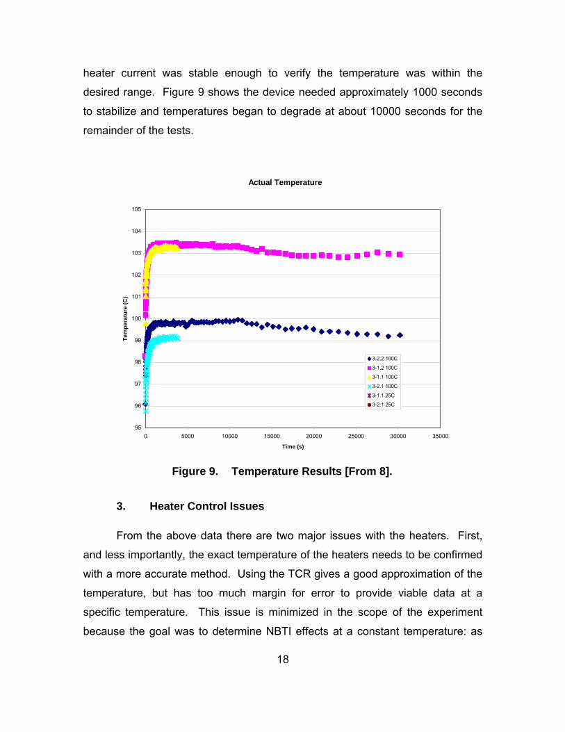
heater current was stable enough to verify the temperature was within the
desired range. Figure 9 shows the device needed approximately 1000 seconds
to stabilize and temperatures began to degrade at about 10000 seconds for the
remainder of the tests.
Actual Temperature
95
96
97
98
99
100
101
102
103
104
105
0 5000 10000 15000 20000 25000 30000 35000
Time (s)
Tem
pera
ture
(C)
3-2.2 100C
3-1.2 100C
3-1.1 100C
3-2.1 100C
3-1.1 25C
3-2.1 25C
Figure 9. Temperature Results [From 8].
3. Heater Control Issues
From the above data there are two major issues with the heaters. First,
and less importantly, the exact temperature of the heaters needs to be confirmed
with a more accurate method. Using the TCR gives a good approximation of the
temperature, but has too much margin for error to provide viable data at a
specific temperature. This issue is minimized in the scope of the experiment
because the goal was to determine NBTI effects at a constant temperature: as
19
long as the temperature was constant, the temperature error would be applied
over the scope of the testing and not impact the NBTI results. The second issue
of heater control has more potential for larger experimental variation. With no
way to control the temperature over the course of the experiment there was no
guarantee the device was under the same thermal stress for the period of data
collection. This would suggest data could have been taken under different
thermal stresses, and the results would not accurately indicate the effects of
NBTI under controlled conditions. It could have been for this reason previous
data collected did not correlate with classical research.

20
THIS PAGE INTENTIONALLY LEFT BLANK

21
III. SOLUTION THEORY
A. CONTROL THEORY OVERVIEW
This section will address the general control theory required to maintain
stability in a simple system. For the purposes of this experiment, it is assumed
purely resistive electrical components (like the resistors in the AFRL test bed) do
not exhibit any inductive or capacitive characteristics and store energy in no
form.
1. System Analysis
The basic problem is the need to find a method to maintain the specific
lattice temperature generated by the resistor constant for the duration of the
testing. In previous research, the value of resistance (measured by differential
voltage) was observed to fall over a long period of testing. The reason behind
the decline in resistance is not addressed in this research. The issue is
maintaining test temperature constant. In previous testing the temperature
required was determined by using the temperature coefficient of resistivity to
determine the required voltage drop across the resistor. With this value
calculated, a constant current was then applied and the voltage drop measured
to determine the experimental temperature. However, during the experiment the
measured voltage did not remain constant, and no system was in place to return
the voltage to the desired value to maintain the constant thermal stress required.
a. Closed Loop Systems
During testing where parameters of a system can change over the
course of operation, closed loop feedback is desired to ensure the system is
continually corrected to maintain the desired output. The advantage of a closed
loop system is the signal output from the system of interest can be fed back into
a comparator to continuously adjust the input. This continual adjustment will force

22
the system to achieve the desired output. Closed-loop configuration is less
sensitive to disturbances and plant perturbation because of the incorporation of
feedback within the plant [15]. Figure 10 shows a general closed-loop control
system with the major components.
Figure 10. General Closed Loop Control System.
The input is a steady signal that is assumed to be constant for the duration of the
time the plant is in operation. The comparator takes the combination of the input
and the feedback from the sensing device and provides the difference between
the two inputs to the controller. The controller accepts the signal and performs
two general functions. First, the difference between the input and the feedback
from the sensing device is applied to the signal before it enters the plant. Usually
the sensing device output is applied as a form of negative feedback in order to
keep the signal from increasing without bound or rapidly decreasing to zero.
Second, a gain is added to the signal to ensure the input to the plant is
appropriate for the plant to perform its designed function. When the signal
comes from the plant it goes to the output where it can be analyzed and to the
sensing device to feed back into the comparator. While the closed loop plant is
generally more expensive than a plant with no feedback, it is most widely used in
applications where plant variation or noise is expected.
b. Theory Application
To apply a closed loop system solution to a specific plant (where
the term plant is used to describe the system under test) the type and order of
Comparator Controller Plant
Sensing Device
Input Output

23
the system must be understood. In many cases, the order of a plant system can
be difficult to predict based on the actual plant. A mathematical plant model or
experimental results need to be analyzed to determine the order of the plant.
Once the order has been determined, response to stimulation is observed to
assist in predicting plant parameters. When stimulation is applied to a plant the
control engineer can measure a variety of indicators to determine plant
parameters. Time to rise to the final output, time to settle at the final output,
percent overshoot, damping effects, and response time are all metrics used in
plant analysis. With data on these metrics available, the engineer can then
determine the plant order and calculate the forced and natural responses to
outside stimulus. Finally, using this data, the control-loop can be applied or
modified to change the plant forced response and achieve the desired response.
B. SOLUTION FOR AFRL TEST BED
In the case of the AFRL test bed, a solution is necessary to maintain
temperature constant for the duration of testing. Previous experiments used both
the heater and thermistor to determine the TCR and to generate the specific
thermal stress desired during testing. With a closed-loop controller, maintaining
the voltage constant for both the thermistor and the resistor is possible.
1. General Characteristics
Figure 8 shows the HP 4155B is used to apply a current to the resistor
and to the forcing lines of the thermistor. The voltage at the thermistor sensing
pads was measured on each side of the thermistor, and then the difference taken
to determine the voltage drop. For the resistor, the value of the TCR was used to
calculate the voltage bias across the resistor (or the current necessary) to
produce the desired thermal stress. No differential voltage was taken directly
across the resistor because thermistor resistance was more sensitive and
therefore used to calculate bias for the heating resistor. In order to apply a
feedback solution to the heater and thermistor, the differential voltage across the

24
thermistor sensing pads must be measured while the current is being applied to
the heating resistor. Once the current is adjusted to achieve the desired voltage,
this voltage will be the reference for the control system. The feedback will use
the sensing line to compare the reference signal to the actual differential voltage
to measure any difference. Once a difference is detected the comparator can
send the difference into the controller, which will make the adjustment to the
applied current in order to drive the difference between the reference and
detected voltage to zero.
2. Specific Solution
Figure 11 shows the specific set up for a control loop that will maintain the
voltage across the thermistor and heating resistor constant:
Figure 11. Specific Feedback Solution.
The current, i, will be the input into the comparator, represented by the
circle. Once the current is applied to the resistor the output voltage (V) will be
measured by comparing the differential voltages from the sensing pads of the
thermistor at each time interval over the testing period. This voltage
measurement will be compared to previous results in order to determine the
approximate value of voltage at steady state (V0). Once the voltage has reached
a steady state value, this measured value can be entered into the sensing device
in the feedback loop, along with the calculated resistance (RCalc) value, given a
constant applied current and the steady state voltage. At this point the switch on
the sensing line can be shut and negative feedback incorporated into the device.
The feedback sensing line will have two functions. First, it will receive an input of
+
0
Calc
V-VR
-iR i V

25
the measured voltage from the output. Second, it will calculate the resistance
value of the heater given the input current and the output voltage. Initially, the
output voltage will be the same as the steady state voltage and the sensing line
will provide no feedback.
Over a period of time as the resistance value drifts (either up or down) the
calculated resistance value in the sensing line will change with the observed
change in the output voltage (input current will remain constant). The value for
the reference voltage, previously entered into the sensing line will remain
constant. At the next measurement point (depending on the time sequence
between the measurements) the input current will be summed with the value
from the sensing line to provide a new current through the resistor. This new
current will drive the output voltage back towards the originally observed steady
state value, and the sensing line contribution to the input will increase or decline
as required to maintain this value. The rate of increase or decline will depend on
the time interval between measurements and the difference in resistance values
between measurements. If excessive ‘hunting’ is observed (a sinusoidal pattern
for voltage produced by a series of alternating current corrections) a negative
gain can be incorporated into the sensing line to decrease the correction value
applied. In the opposite case, if the drift exceeds the correction from the sensing
line, a positive gain is applied to curb further resistor change.

26
THIS PAGE INTENTIONALLY LEFT BLANK

27
IV. SOLUTION APPLICATION
A. HP 4155B
With the theoretical solution determined the method of application to the
AFRL test bed must be addressed. Test beds provided by AFRL were unbonded
and difficult to work with using Signatone© probes making direct electrical contact
with the thermistor pads. Special equipment (such as a pneumatically stabilized
test bench and a microscope viewing station) is necessary to take readings
directly from the unbonded pads, and variation in the application of probes could
produce experimental variation.
Many of these problems are solved with the use of the HP 4155B with the
Agilent 16442A test fixture. The fixture has a configuration to test a 28 pin DIP
device. By bonding the AFRL test bed to a 28 pin DIP, the Agilent 16442A can
be used to relay data to the HP 4155B. The major advantage of using the test
fixture is the simplicity and consistency. With the test fixture the 28 pin DIP
requires no special stabilization equipment during measurement, and there is no
concern for any physical shifting during longer range testing. The 28 pin DIP can
be installed and removed quickly from the test fixture, allowing more time for
testing the same structure or multiple structures.
The first step is to bond the structure to the 28 pin DIP. Previous research
was conducted with four bonded chips, and these bonded structures were used
to gather NBTI data. The next consideration is to determine the method and
limitations of testing with the HP 4155B.
1. Overview of the HP 4155B
The HP 4155B is an instrument designed to measure and analyze the
specific characteristics of semiconductor devices. Once the measurements are
complete, the instrument is designed for analysis and display of the results [16].

28
The HP 4155B has four source and monitor units (SMUs) to provide a
source for either voltage or current and monitoring capability, two voltage source
units (VSUs) to provide voltage bias, and two voltage measurements units
(VMUs) to measure bias at a specific point with respect to ground. It has the
capability to perform either sweep or sampling measurements [17].
The sweep measurements can be in either linear or log scales, with the
start, stop and step sizes defined by the user. After forcing a start value, a hold
time between steps can also be defined, as well as a delay time before applying
the next forcing value. The sampling measurement is continuous. Voltage or
current changes can be monitored for the device under test while forcing
constant current, voltage, or pulsed constant bias [17].
In order to do any testing, there are three ways to control the functions of
the HP 4155B. The default is to use the HP 4155B with no outside control.
There are a number of capabilities pre-programmed into the machine which will
meet the needs of most standard testing for semiconductor microelectronics. If
the user is attempting to perform a function not available in the pre-loaded
menus, the user must then customize instructions to the specific need necessary
for the testing. The first method to provide custom instructions can be defined by
the user by directly interfacing with the HP 4155B (via keyboard) and
programming the test device with Instrument BASIC (IBASIC™). IBASIC™ is the
native controller language used by Agilent test equipment to run customized
programs. The second method is to use an external computer connected to the
HP 4155B with a General Purpose Interface Bus (GPIB). Also known as the
IEEE-488 bus, the GPIB was developed by Hewlett Packard to connect testing
instruments to computers for further analysis using programs not available on the
test equipment. For this experiment the software package Laboratory Virtual
Instrumentation Engineering Workbench (LabVIEW©) can be used to take
advantage of the visual programming language in order to apply the feedback
necessary to the testing. Each method has advantages and disadvantages
which will be discussed in detail.

29
B. INSTRUMENT BASIC
Instrument BASIC is a way to control Agilent systems directly. The
capability is built into the HP 4155B and the equipment has an internal controller
aligned for immediate use. IBASIC™ will run a program that controls the HP
4155B and any other test instrumentation connected via interfaces. IBASIC™ is
a subset of HP BASIC, therefore any programs in IBASIC™ can run on a HP
BASIC controller with little or no modification [18].
1. Description and Abilities
a. General Overview
There are two methods of controlling the HP 4155B with IBASIC™:
using an external computer with a GPIB card or using the built-in IBASIC™
controller. After choosing one of these methods, the user must then select the
command mode in order to execute the desired program. The first mode is the
Standard Commands for Programmable Instruments (SCPI) command mode.
The default mode for the HP 4155B, the user can control all of the functions of
the HP 4155B and attached equipment during testing. The second choice is the
Fast Language for Execution (FLEX) command mode. The user controls only
the measurement functions of the HP 4155B in this mode. The advantage of the
FLEX mode is the increased speed over the SCPI mode. Finally, the user can
choose the syntax command mode. This mode was incorporated to run
programs from the HP 4145A/B on the newer test equipment without modification
[18].
With the method of control and the command mode selected, the
user can begin programming. Mode selections allow all programming to be
accomplished with the softkeys available on the face of the instrument, or with an
external keyboard plugged into the machine. A help function is available for
standard IBASIC™ commands, as well as standard SCPI commands and SPCI
commands available only for the HP 4155B [18].

30
The challenge is to create a program that has the ability to measure
the voltage across the heating resistor and make changes to the current applied
in order to keep the voltage drop constant. Specifically, the program will provide
instruction to the HP 4155B to apply a constant current across the heating
resistor via one of the SMUs, read the voltage drop across the thermistor with the
VMUs, calculate any change in resistance due to drift, and adjust the applied
current accordingly. Because the FLEX mode only allows control of the
measurement functions, all programming needs to be in the SCPI mode. The
SCPI mode has the ability to set all desired parameters and execute the program
in the order desired to achieve the measurement as well as the updated
corrections during the applied thermal stress. The basic approach is explained
below.
b. Programming Concerns
In order to program the HP 4155B to perform the measurement
scenario it is necessary to understand the set-up, execution and data transfer
operations necessary to accomplish the overall task. The first part of the
measurement program is the initial set-up. To program a set of initial conditions
for a measurement scenario, the SCPI commands can be used to set up the
individual screens (menus) inside the HP 4155B to perform the basic tasks.
There are three different ways to perform these tasks. First, data for
measurements or voltage/current stress can be loaded from a disk, a central
server, or internal memory and directly used in the scenario. This is
accomplished with SCPI programming to create previously defined and stored
routines that will be called in the measurement scenario. Second, data can be
loaded as described previously, but the data is manipulated before the
measurement scenario is initiated. Third, all of the settings can be defined by
SCPI programming in the measurement sequence without loading any previously
defined data. The set-up includes assigning an input/output path to control the
HP 4155B (either via an external controller using a GPIB cable or the internal

31
IBASIC™ controller), setting the mass storage device the HP 4155B will
reference in any load/save commands, loading previously defined data, and
making any changes prior to executing the measurement scenario [18]. A
summary of the commands to change various set-up parameters is shown in
Figure 12.
Setup Screen Command Subsystem
CHANNELS: CHANNEL DEFINITION :PAGE:CHANnels[:CDEFinition]
CHANNELS: USER FUNCTION DEFINITION :PAGE:CHANnels:UFUNction
CHANNELS: USER VARIABLE DEFINITION :PAGE:CHANnels:UVARiable
MEASURE: SWEEP SETUP :PAGE: MEASure[:SWEep]
MEASURE: SAMPLING SETUP :PAGE:MEASure[:SAMPling
MEASURE: PGU SETUP :PAGE:MEASure:PGUSetup
MEASURE: MEASURE SETUP :PAGE:MEASure:PGUSetup
MEASURE: OUTPUT SEQUENCE :PAGE:MEASure:PGUSetup
DISPLAY: DISPLAY SETUP :PAGE:DISPlay[:SETup]
DISPLAY: ANALYSIS SETUP :PAGE:DISPlay:ANALysis
STRESS: CHANNEL DEFINITION :PAGE:STRess[:CDEFinition]
STRESS: STRESS SETUP :PAGE:STRess:SETup
Figure 12. Summary of Setup Screens for the HP 4155B [From 18].
With loaded Setup values the measurement execution can begin. A
measurement is executed with the ‘:PAGE:SCONtrol[:MEASurement]:SINGle’
command to the HP 4155B in the body of the main SCPI program. The
‘:REPeat’ ending (vice ‘SING’) is used to repeat a measurement, and the
‘:APPend’ ending is used to append a measurement. The HP 4155B has the

32
ability to execute either a sweep or sampling measurement. The execution
phase is also where the current stress is applied to the heating resistor. With the
‘:PAGE:SCONtrol:STRess[STARt]’ command, the stress is applied from the pre-
loaded source or from the previously defined stress in the program memory [18].
The final data manipulation requirement in the measurement
scenario is the data transfer option. In the setup phase it may be necessary to
load previously stored programs in order to set initial conditions for measurement
parameters or applied stress. The programmer must first specify the storage
device in use with the ‘:MMEMory:DESTination’ command. Setup data is then
loaded with the ‘:MMEMory:LOAD:STATe command, and measurement data
with the ‘:TRACe’ command (vice the ‘STATe’ command) at the end of the load
sequence. Setup and measurement data is stored in the same way (same third
parameter), but using the ‘MMEMory:STORe:’ sequence for storage [18].
2. Issues Encountered
A basic programming approach is now possible using the general
guidance explained above. Figure 13 shows a basic flow chart for programming
the sequence of events. There are a few notable details concerning the setup
and flow of data collection. Once the initial test gear set up is accomplished the
bias is applied across the heater and the change in voltage (ΔV) is measured. In
the previous research it was noted that the heater did not reach a steady state
value until about 1000 seconds into the testing [8]. Therefore, a time interval
needs to be selected based on previous work as a starting point to choose a
steady state ΔV to use as a baseline value. This time delay will allow the heater
to reach steady state. Once this baseline is established NBTI measurements
can be recorded at the steady thermal stress.
A second consideration is the comparison between the most current ΔV
and the pre-recorded steady state ΔV. If there is a change between the values a
correction current bias will be applied in order to bring the most recent ΔV back
to the steady state value. There are several issues with this correction. First, a
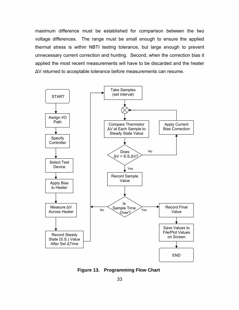
33
maximum difference must be established for comparison between the two
voltage differences. The range must be small enough to ensure the applied
thermal stress is within NBTI testing tolerance, but large enough to prevent
unnecessary current correction and hunting. Second, when the correction bias it
applied the most recent measurements will have to be discarded and the heater
ΔV returned to acceptable tolerance before measurements can resume.
Figure 13. Programming Flow Chart
Assign I/O Path
Specify Controller
Select Test Device
Apply Bias to Heater
Measure ΔV Across Heater
Record Steady State (S.S.) Value After Set ΔTime
Take Samples (set interval)
Compare Thermistor ΔV at Each Sample to
Steady State Value
Record Sample Value
Record Final Value
Save Values to File/Plot Values
on Screen
START
Apply Current Bias Correction
END
Does ΔV = S.S.ΔV?
Is Sample Time
Over? Yes No
No
Yes

34
The major drawbacks with the IBASIC approach are the lack of knowledge
of the programming language and the reduced flexibility in combining the NBTI
measurements with the temperature feedback mechanism. The primary difficulty
in the IBASIC approach is becoming practiced enough with the language to
construct a program which will perform the desired functions. Preliminary work
indicated a program with approximately 200 to 400 lines of code would be
necessary to set up conditions simply to control the thermal stress condition of
the testing. No consideration was given to the additional programming
necessary to conduct the NBTI experiments. While the programming could be
conducted in a simulated controller, the assignment of variables and paths to the
HP 4155B would require more time to establish. Once the program was
operational, testing would include multiple test runs over longer time periods to
establish intervals for time to steady state, differences between voltage changes
and delays after applying bias corrections. These changes would have to be
incorporated into the source code, which would then need to be reloaded to the
HP 4155B for further testing. Also, any follow on research would be required to
work in the established IBASIC™ testing frame, which could prove difficult to
understand. Because of the initial programming time required, lack of flexibility in
changes, and the non-integration of the NBTI portion of the testing, the IBASIC™
approach was not used in this research.
C. LABVIEW©
A much more user friendly method of controlling the HP 4155B was with
the use of LabVIEW©. LabVIEW© has a variety of applications that are specific to
each device under control, and are usually provided by the device manufacturer
to ease programming concerns and allow the user maximum flexibility in the use
of the instrument.

35
1. Overview
LabVIEW© requires an external processor capable of running the main
program with a GPIB interface to give commands to the device being controlled.
The processor must be connected to the device and communication is
established either with equipment specific drivers provided by manufacturers or
code written specifically to interface the processor to the test device. Once the
test equipment is verified to be under external control, a program written in
LabVIEW© will control the device.
Using a visual programming medium LabVIEW© provides a wide variety of
standard icons to perform specific functions within the overall program. By
selecting a specific icon the user can then ‘drag and drop’ the icon into a
workspace. Icons are then interconnected, or ‘wired’, in the virtual environment.
The selection of icons and the order of connection will determine the tasks the
testing device is to perform.
To provide the user with a simple environment to enter testing conditions
and monitor program progress, a virtual instrument is constructed in parallel with
the icon driven workspace. This virtual instrument provides an interface where
the user can enter initial conditions, monitor progress, show testing conditions
and output graphs or charts during and after data collection is complete and
these changes are incorporated into the program. Data can be saved to a file
and then transferred to another program for analysis. The advantage of the
virtual instrument is the user can change conditions of the testing without the
need to enter the programming space and make changes to the internals of the
program. When different testing is desired, or different initial conditions require
change, the virtual instrument can be changed to reflect the needs of the user.
This allows a variety of testing under different conditions by only adjusting the
face of the virtual instrument before the test run starts.

36
2. Application for the HP 4155B
The HP 4155B had a variety of features that made programming in
LabVIEW© advantageous. First, connection between the processor and the HP
4155B was made simple with an interface on the HP 4155B previously designed
for the GPIB hardware and connector cable. Second, Agilent technologies
provided the drivers and a selection of instrument specific LabVIEW© applications
to streamline programming efforts. This saved a huge amount of time by
enabling the user to incorporate these previously programmed standard
instrument capabilities into the main testing program very efficiently. Finally, the
HP 4155B could be initialized in the local mode and then controlled by LabVIEW©
for the experimental run. This again saved programming time because the
testing program did not have to set initial instrument parameters, but simply look
for the established conditions and control the operation of the device while
testing was in progress.
3. Experimental Setup
After establishing connection between the processor and the HP 4155B,
LabVIEW© was used to program the instrument. The initial conditions were
established in the local mode and then the HP 4155B was controlled by
LabVIEW© for the duration of the testing.
In order to hold the thermal stress constant during NBTI testing, the initial
concept was to incorporate current feedback into the HP 4155B during NBTI
testing. After discussions with Agilent technical support and with various
independent testing a critical limitation of the HP 4155B was discovered. The
machine does not have the capability to alter any parameters during the course
of testing. This means any necessary feedback cannot be incorporated into the
heater while the test run is in progress.
To overcome this limitation, the next best option is to program the HP
4155B to run a series of shorter tests, and to evaluate/adjust the feedback

37
current between the test runs. This option is not as desirable as a single,
continuous test run, but has the advantage of adjusting the update times as
necessary during the testing. If, for example, an eight hour test run is desired,
testing intervals could be broken into a series of 24 runs of 20 minutes each. In
between each 20 minute interval the temperature of the heater (determined by
voltage differential across the thermistor and the pre-determined TCR) would be
evaluated and current adjusted accordingly in order to maintain a constant
thermal stress.
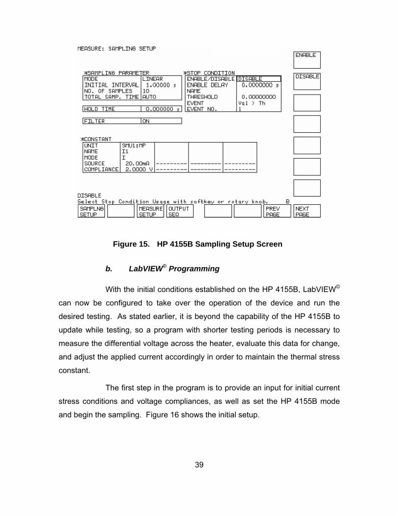
a. HP 4155B Initial Setup
The first step in the process is to establish the initial HP 4155B
setup for applying the current and measuring the feedback. Figure 14 shows the
initial setup screen in concept testing.
Figure 14. HP 4155B Channel Definition Screen

38
The ‘MEASUREMENT MODE’ field will be sampling to collect the data at
constant test conditions. The ‘CHANNELS’ fields will be set to apply the desired
stress and measure the differential voltage across the resistor. Current will be
applied via SMU1 in the “I” mode at a constant value. The voltage difference is
monitored with VMU1 and VMU2 in the differential voltage (DVOLT) mode. The
Ground Detection Unit (GNDU) provides both a zero voltage reference value and
a sink for the current to complete the circuit through the resistor. Figure 15
shows the second initial conditions screen. This is the screen where testing
interval and initial stress conditions are established. In the ‘SAMPLING
PARAMETERS’ section the fields are as follows. The ‘MODE’ remains linear to
stay consistent with the sampling mode established on the Channel Definition
screen. The ‘INITIAL INTERVAL’ is the interval between samples. Because the
time to sample is on the order of one millisecond, any interval above 10
milliseconds will be satisfactory for testing. ‘NO. OF SAMPLES’ works with initial
interval to establish the total sample time in the automatic mode (shown below),
or the total sample time can be set manually (not recommended). The ‘HOLD
TIME’ is the amount of time that test conditions will be applied before sampling
begins. ‘FILTER’ set to ‘ON’ reduces the amount of peripheral circuit noise
encountered while sampling. ‘STOP CONDITIONS’ are not used in this testing.
In the ‘CONSTANT’ section, UNIT, NAME, and MODE are defined on the
Channel Definition page. The ‘SOURCE’ field defines the initial current stress
applied to the heater, and the ‘COMPLIANCE’ field sets the maximum voltage
the HP 4155B will record in the measurement mode. Because the VMU
differential voltage mode will be used, the maximum compliance is two volts [17].
39
Figure 15. HP 4155B Sampling Setup Screen
b. LabVIEW© Programming
With the initial conditions established on the HP 4155B, LabVIEW©
can now be configured to take over the operation of the device and run the
desired testing. As stated earlier, it is beyond the capability of the HP 4155B to
update while testing, so a program with shorter testing periods is necessary to
measure the differential voltage across the heater, evaluate this data for change,
and adjust the applied current accordingly in order to maintain the thermal stress
constant.
The first step in the program is to provide an input for initial current
stress conditions and voltage compliances, as well as set the HP 4155B mode
and begin the sampling. Figure 16 shows the initial setup.
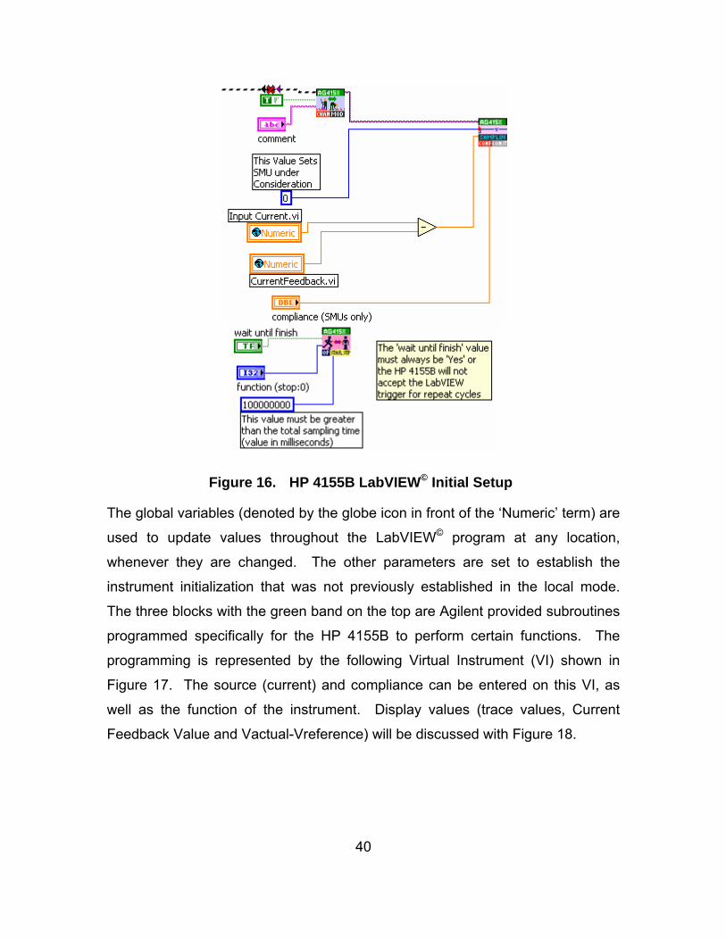
40
Figure 16. HP 4155B LabVIEW© Initial Setup
The global variables (denoted by the globe icon in front of the ‘Numeric’ term) are
used to update values throughout the LabVIEW© program at any location,
whenever they are changed. The other parameters are set to establish the
instrument initialization that was not previously established in the local mode.
The three blocks with the green band on the top are Agilent provided subroutines
programmed specifically for the HP 4155B to perform certain functions. The
programming is represented by the following Virtual Instrument (VI) shown in
Figure 17. The source (current) and compliance can be entered on this VI, as
well as the function of the instrument. Display values (trace values, Current
Feedback Value and Vactual-Vreference) will be discussed with Figure 18.

41
Figure 17. HP 4155B LabVIEW© Virtual Instrument for Current Feedback

42
Figure 18. HP 4155B LabVIEW© Current Feedback Controller

43
The final portion of the LabVIEW© program deals with the collection
of the most recent test data, calculation of the differential voltage, adjustment and
application of the feedback current, and commencement of the next testing cycle.
Once the test cycle commences, the data is collected in an array within the HP
4155B. Upon conclusion of the test the differential voltage sample points are
transferred into a LabVIEW© buffer. The initial data point is truncated as the
beginning of the test to this point is the interval where the HP 4155B ramps up
the applied current from zero amps to the desired test level. Because this data
point is not at a constant value it is of no use for analysis and is therefore
discarded. After this point, the data is saved in a file and all subsequent data
from later runs is appended to the same file (sans the first value) for later
analysis.
The differential voltage data is then averaged to determine an
average differential voltage value over the testing period. This most recent
differential voltage value is then used in two separate analyses. The first is a
comparison to the reference differential voltage that was found in baseline
testing. This baseline voltage is taken from each individual AFRL device to
capture the exact parameters of the heater in use for that particular device. This
also determines the amount of differential voltage necessary to provide the
thermal stress desired for testing. The value for the reference voltage is entered
into the program, and the difference between the most recent differential voltage
and the reference differential voltage will determine the amount of current
feedback necessary. While previous testing theory in IBASIC™ advocated a
waiting period to steady state, this value can be entered at the beginning of
testing and no delay is necessary before data collection begins.
The second place the most recent differential voltage value is used
is when determining the most recent resistance value. Because the resistance
drifts over long periods of testing, the value of resistance must be re-calculated to
compensate for the drift. By taking the initial input current and the feedback
value (summed in a negative feedback loop), the total applied current is

44
available. The most recent differential voltage is then divided by the total applied
current to give the value of the resistance after the most recent test run.
With the difference between the actual and reference differential
voltage and the most recent resistance value, a feedback current value can be
calculated. This feedback value is then added to the last feedback value to
provide a running total of feedback current necessary to apply at the beginning of
the next NBTI testing cycle. The global value of feedback current will update
before the next test cycle begins, and the process repeats for the programmed
number of cycles until testing is completed.

45
V. RESULTS AND CONCLUSIONS
A. TESTING RESULTS
Once the programming was completed the testing could begin. The first
consideration was to test the concept to ensure the LabVIEW© program
performed the desired function. Once concept testing was complete and
satisfactory additional testing would be conducted on the AFRL test bed.
1. Concept Testing
With the LabVIEW© program complete a proof of concept test cycle is
conducted. To prove the feedback loop will force differential voltage to the
reference value, a variable resistor (a decade box in this case) is used to
simulate the heater in the circuit. The differential voltage is taken across the
resistance and recorded during the period of measurement. Eight test cycles
consisting of 50 samples (one sample taken every 0.1 second for a total of 5
second cycles) were conducted, and resistance was both increased and
decreased to demonstrate the capability of the feedback loop. Figure 19 shows
the graphical results of the test.

46
Differential Voltage Over Time
0.34
0.36
0.38
0.4
0.42
0.44
0.46
0.48
1 51 101 151 201 251 301 351Time (in tenths of seconds)
Diffe
rent
ial V
olta
ge (i
n V
olts
)
Figure 19. Data Summary of Test Cycles
At the beginning of the test cycle heater current is set at 20 milliamps (mA),
reference differential voltage is 0.400 volts, and resistance in the decade box is
set to 22 ohms (which is measured accurately at 22.80 ohms). The test cycle
then commences. The first run returns an expected differential voltage value of
0.456 volts, based on the initial resistance and applied current (point 1). When
the first five second period is completed the differential voltage data is evaluated
and the differential voltage is forced to the reference value of 0.400 volts by
adjusting the applied current to 17.54 mA (point 2). Resistance is not changed
for the duration of the second and third cycle to demonstrate current will not
change and voltage is maintained at 0.400 volts when resistance remains
constant. At the beginning of the fourth cycle resistance is increased to 23 ohms
on the decade box (accurately measured at 23.32 ohms) which accounts for the
voltage increase to 0.409 volts (point 3). Upon the completion of the fourth cycle
the applied current is re-adjusted to 17.21 mA to force the voltage to 0.401 volts
1
2
34
56
7

47
(point 4). The reason voltage is not forced back to exactly 0.400 volts is because
the initial 2 to 5 data points are skewed due to the spike on the graph as
resistance was changed. At the end of the fifth cycle and in the beginning of the
sixth cycle the resistance was moved on the decade box from 23 ohms (23.32
ohms) to 21 ohms (20.78 ohms measured accurately—shown at point 5). This
forces the differential voltage for the remainder of the fifth run to be 0.358 volts
(between points 5 and 6). At the end of the sixth cycle the current is adjusted to
18.35 mA, which forces the differential voltage to 0.381 volts (point 6). Again, the
reason current is not adjusted back to the reference value of 0.400 volts is
because all of the differential voltage data in the previous cycle is averaged to
give a new differential voltage value, so the change in resistance (and
subsequent changes in differential voltages) are included in the average. In the
seventh cycle resistance is not varied and at the commencement of the eighth
cycle (point 7) the applied current is adjusted to 19.25 mA to force the differential
voltage back to the reference value of 0.400 volts.
This concept test demonstrates that should resistance vary during one of
the testing cycles, the current applied to the heater will be adjusted accordingly to
force the differential voltage back to the reference value. It makes no difference
if the resistance is raised or lowered because the control loop accounts for
changes in either direction. In this test case the resistance changes were large
and sudden, where actual data in extended testing show the temperature drift
(resistance drift) to be very gradual over a longer period of time. Because the
average of all of the data is taken for the previous cycle, the correction to the
applied current will be adjusted to minimize any overshoot and time to steady
state. As seen in Figure 9 the temperature drift was on the order of a degree
over a period of five hours, so the corrections to applied current will not be drastic
or wide ranging from initial applied values.

48
2. Delay Time between Test Runs
With concept testing consisting of a pre-determined number of machine
resets, the delay time between testing is an additional fact important to note. In
effect, the LabVIEW© program is similar to a user waiting until a testing run is
over and cycling the machine manually to begin another test run. Because the
thermal stress will be absent from the heater between cycle times, the times
need to be noted and compared to the duration of the testing runs.
To accurately determine the time between current stresses to the heater
an oscilloscope was connected to each side of the differential voltage monitoring
units. While the heater was under current stress the oscilloscope measured a
high value, and when the stress was removed the measured value was low. Five
series of tests were performed with five series of stresses (which provided four
intervals when stress was removed). The test results are shown in Figure 20.
Figure 20. Typical Testing Series to Determine Cycle Delay
Each delay period was then examined with a larger scale as shown in Figure 21.

49
Figure 21. Cycle Delay For A Single Cycle
These measurements were then averaged over all tests to determine a working
delay time. The results are shown in Table 4. All delay times are in milliseconds.
Table 4. Delay Measurements
1st Delay 2nd Delay 3rd Delay 4th Delay
Test #1 876 885 888 876
Test #2 887 880 878 869
Test #3 881 876 889 872
Test #4 892 873 881 884
Average Delay 880.44 ms.

50
This delay value is important when examining the testing cycle under
consideration. With a testing cycle of 10 seconds or less, the delay time between
cycles is a significant percentage of the total, and the heater is without stress for
that time. However, when testing cycles are on the order of five to twenty
minutes the delay time is a very small percentage of the total testing time and the
amount of time the heater is without current stress is deemed negligible during
the course of the overall test.
3. AFRL Test Device Testing
With the concept testing completed and the delay time known, the AFRL
testing device is placed under test. Using the test setup shown in Figure 8 the
device was put under test. From Table 3 a value of 1.41 volts (correlating to
approximately 75 degrees Celsius) across the thermistor was selected for the
reference voltages in the testing cycles. The resistance of the heater was
measured to determine the specific heater current required to create a differential
voltage across the heater of 1.41 volts. The heater resistance was measured at
22.20 ohms (at room temperature). With this resistance, a current of 63.50 mA
will produce the desired differential voltage.
Two tests were conducted, a one hour and an eight hour test. A cycle
time of five minutes was selected to allow the heater time to begin to heat up, but
not quite reach equilibrium. Sample intervals were set at five seconds apart (for
a total of 60 samples per cycle). In the one hour test twelve cycles were used,
and 96 cycles in the eight hour test. The following figures show the results of the
two tests.

51
Thermistor Differential Voltage
1.406
1.408
1.41
1.412
1.414
1.416
1.418
1 61 121 181 241 301 361 421 481 541 601
Number of Samples (every 5 seconds)
Diff
eren
tial V
olta
ge (v
olts
)
Figure 22. One Hour Test of Thermistor Differential Voltage
At the beginning of the stress period the differential voltage rises as the heater
(and thermistor) begins to feel the thermal stress. With the end of the cycle the
current is adjusted based on the differential voltage values and re-applied.
Figure 22 shows the rises of differential voltage grows steadily smaller as the
voltage across the resistor is forced to the reference value of 1.41 volts. There
was a curious spike noted at the 15 and 45-minute points, but this is simply
because the HP 4155B auto calibration feature was not disabled prior to testing,
and the calibration time of 20 to 30 seconds allowed the heater to cool before
testing resumed.
In order to maintain the voltage constant the current value would decrease
upon each application (at the beginning of the test) and then remain relatively
constant for the remainder of the cycle. This trend is recorded in Figure 23. The
beginning value for current was 63.50 mA for the first five minutes. Upon each
re-evaluation, resistance increased and the current was decreased to force
differential voltage to the reference value. Because of the limitations of the HP

52
4155B, this current was only applied at the beginning of each five minute test
cycle, which is the reason for the time delay when coming to steady state. If a
quicker steady state time is desired, shorter testing cycles are necessary, but this
may also increase variation at steady state values.
Changes in Current
0.063
0.0631
0.0632
0.0633
0.0634
0.0635
0.0636
1 2 3 4 5 6 7 8 9 10 11 12
Number of Adjustments (every 5 minutes)
Cur
rent
(am
ps)
Figure 23. One Hour Test Heater Current Values
Eight hour testing followed the same general pattern. Figure 24 shows the
thermistor differential voltage over the eight hour testing period. Like the one
hour test, the initial values are very high as the resistor receives the initial stress
and begins to come to steady state. After approximately ten minutes the
differential voltage value is corrected to an approximately steady state value
(± 0.004 volts, until approximately 6.4 hours when the differential voltage
increased slightly). For the remainder of the test there is some ‘hunting’ noted as
the resistor is continually stressed and relaxed, possibly causing thermal
changes which would require more or less current, depending on the previous
amount of current applied.

53
Thermistor Differential Voltage
1.4081.4091.41
1.4111.4121.4131.4141.4151.416
1 481 961 1441 1921 2401 2881 3361 3841 4321 4801 5281
Number of Samples (every 5 seconds)
Diff
eren
tial V
olta
ge
(vol
ts)
Figure 24. Eight Hour Test of Thermistor Differential Voltage
Figure 25 shows the current values over the eight hour testing period. It is
interesting to note that after five hours of testing the average current value rises
by approximately 50 microamps in order to keep the differential voltage value at
steady state. This would suggest either a change in the heat gradient or some
sort of current leak-by after a fixed amount of testing.
Changes in Current
0.063150.0632
0.063250.0633
0.063350.0634
0.063450.0635
0.06355
1 6 11 16 21 26 31 36 41 46 51 56 61 66 71 76 81 86 91 96
Number of current changes (every 5 minutes)
Cur
rent
(am
ps)
Figure 25. Eight Hour Test Heater Current Values

54
In an attempt to reduce the amount of cyclic variation in the application of
current, a longer application period (ten minutes) was attempted with the
following results:
Thermistor Differential Voltage
1.4081.4091.41
1.4111.4121.4131.4141.4151.4161.417
1 481 961 1441 1921 2401 2881 3361 3841 4321 4801 5281
Number of Samples (every 5 seconds)
Diff
eren
tial V
olta
ge (v
olts
)
Figure 26. Eight Hour Test of Thermistor Differential Voltage, 10 Minute Stress Periods
The cyclic variation is reduced and the amount of difference between the desired
value (1.41 volts) and recorded values is on average less than the five minute
testing period. This shows that a longer data run allows the AFRL device to
reach more of a ‘steady state’ value in each run and the current correction does
not need to be as great. Figure 27 shows the current corrections. These
corrections more closely match data presented in Figure 9 which displays a
gradual decrease in temperature. The heater current changes in Figure 27 show
a gradual increase over the testing period, which indicates some change in
resistance which would cause differential voltage (and therefore temperature) to
fall over the eight hour testing period.

55
Changes in Current
0.0632
0.06325
0.0633
0.06335
0.0634
0.06345
0.0635
0.06355
1 4 7 10 13 16 19 22 25 28 31 34 37 40 43 46
Number of Current Changes (every 10 minutes)
Cur
rent
(am
ps)
Figure 27. Eight Hour Test Heater Current Values, 10 Minute Stress Periods
To find the magnitude of the change in temperature, the previously
determined average TCR of 0.0028 [8] is used to calculate the maximum
temperature difference that could be expected, given the maximum voltage
difference over the period of testing. In Figure 24 the maximum differential
voltage recorded after the heater had reached steady state was 0.0013 volts
(between samples 4956 and 4957). Using the values found in Table 2 [8] the
average change in voltage per degree (averaged between Device A and Device
B) is 47.88 degrees Celsius per volt. Which means a change of 0.0013 volts
would correlate to a temperature change of 0.062 degrees Celsius. In Figure 26
the maximum voltage change is 0.0007 volts (between samples 952 and 953),
which correlates to a temperature change of 0.033 degrees Celsius. In both
cases, the temperature is held to approximately 5% of one degree Celsius.
B. CONCLUSIONS
The current feedback correction is successful in that current is calculated
and adjusted as resistance drifts, but the solution is not ideal. Because this

56
solution requires a longer test to be broken into a series of shorter testing
intervals, the device is forced to undergo a cyclic stress and testing profile. While
there may be no impact to the device with this application and removal of current
to the heater, the experiment data collected from NBTI testing could be skewed
due to the cycles.
1. LabVIEW© Conclusions
LabVIEW© was very user friendly and made programming intuitive when
designing a solution to the current feedback issue. The virtual instrument made
altering initial conditions easy and eliminated the need to enter the program to
make changes internally. There are a few other values that could be
incorporated on to the face of the virtual instrument so all parameters of interest
are either displayed during testing or set before the testing cycle begins
(reference voltage, for example, must be changed internally in the program). The
time between cycles will have minimal impact on the longer testing cycles, but
with shorter cycles, it could pose a problem.
The cyclic differential voltage remained very close to original values and,
with the previously found TCR, the temperature variation would be less than five
percent of one degree Celsius. Should testing require a tighter thermal stress
the feedback solution could be altered to account for later data, or take a different
portion of differential voltage to perform the average used in the correction
calculation.
Because the heater current solution was conducted in LabVIEW© the
remainder of the NBTI testing can be incorporated into the heater program.
Initial conditions for testing can be set locally, and during testing data can be
gathered via LabVIEW© sub-routines which would either display the results or
save the data points to a file for further review.

57
2. HP 4155B Conclusions
For the earlier NBTI testing the HP 4155B was a very good choice. With
the ability to stress while measuring data the HP 4155B could collect the desired
data for analysis. However, with the observed drift in differential voltage across
the thermistor, a need to adjust heater current during testing is necessary to
maintain a constant thermal stress. The HP 4155B is incapable of making this
adjustment during a measurement cycle and must be adjusted and re-started to
maintain the thermal stress constant. In the interest of maintaining thermal
stress as continuous and constant as possible, the HP 4155B is not the ideal test
instrument. Valid test data can be gathered from this instrument, but future
research should be conducted with an instrument that has a stress adjustment
capability while measurement is underway.
3. Areas for Further Study
With the ability to apply a constant thermal stress, the initial testing can be
conducted again, and results from both tests compared to determine the impact
of the temperature drift. There are also additional areas for further study
a. Initial Temperature Calibration
The TCR was initially calculated by heating an unbonded AFRL test
device on a Hot Chuck heating device. There was no indication that the Hot
Chuck was accurately calibrated to deliver the desired temperature, the amount
of temperature drift over time, or the temperature variation range over time.
Further work to calibrate a heat source would provide a more exact TCR which
would lead to a more precise thermal stress requirement to produce a
temperature.
b. Control Application
The control solution is successful in forcing the value of the
differential voltage to the desired value, but ‘hunting’ observed in the above plots

58
shows the control loop may need to be adjusted if closer tolerance is required.
Possibly the time interval for data collection could be changed, or the number of
differential voltage values used in the calculation of the feedback current.
Tolerance could be reduced to ranges desired, but it may be difficult to
incorporate a single control solution to a device under test that needs to initially
come to equilibrium under stress, and is then cycled for the remainder of testing.
c. Feedback Verification
Temperature feedback was verified to remain within 5% of one
degree Celsius, but impact on the actual PMOS component was not shown. A
record of diode gate-drain voltage over the stress period would show any
changes with thermal stress, which would indicate that thermal stress change is
still great enough to impact the device under test. Further programming in
LabVIEW© to record this data and plot over time could be used to verify the
effectiveness of the feedback loop.
d. Further NBTI Testing with Integrated Heater Control
NBTI testing can be continued with a constant thermal stress. The
tests in question were the long term tests at 25 and 100 degrees Celsius for
periods of three hours and beyond. By breaking up the testing into shorter cycles
data could be gathered with the thermal stress constant and compared to the
previous data to determine changes (if any). An important part of this testing
would be to determine if the cyclic effect on stresses had any effect on the NBTI
data. A control run could be performed using the previous methods and
additional testing using the cyclic approach for comparison. In addition, the
Charge Pumping or Direct Threshold Voltage Measurement could be attempted
and the results compared to previous research without and with temperature
feedback.

59
LIST OF REFERENCES
[1] Department of Defense. (1996, 31 December 1996). Test Method Standard: Microcircuits.
[2] H. Livingston, “The current state of the semiconductor industry and DoD weapon system dependence on off-shore products,” in Diminishing Manufacturing Sources and Material Shortages 2005, 2005.
[3] Defense Science Board Task Force. (2005, February 2005). High Performance Microchip Supply.
[4] Institute for Defense Analyses, “Resource & Support Analyses,” vol. 2006, 2006.
[5] G. Carlson, “Trusted Foundry: The Path to Advanced SiGe Technology,” in 2005, pp. 9-12.
[6] D. Pierce. (2005), Module description.
[7] IBM Systems and Technology Group. (2005), 130-nm Foundry Technology Platform: CMOS, RF CMOS and SiGe BiCMOS.
[8] C. M. Schuster, “Negative Bias Temperature Instability (NBTI) Experiment,” M.S. thesis, Naval Postgraduate School, Monterey, CA, 2006.
[9] S.O. Kasap, Principles of Electronic Materials and Devices, 2nd ed. New York: McGraw-Hill, 2002, p. 745.
[10] A.S. Sedra and K.C. Smith, Microelectronic Circuits, 5th ed. New York: Oxford University Press, 2004, p. 1283.
[11] M.A. Alam, “A Simple View of a Complex Phenomena,” Reliability Physics Tutorial Notes, 2006, p. 191.
[12] S. Mahapatra, “Electrical Characterization and Modeling of Negative Bias Temperature Instability in p-MOSFET Devices,” 2006, p. 192.
[13] T. Nigam, “Lifetime Enhancement Under High Frequency NBTI Measured on Ring Oscillators,” IEEE International Reliability Physics Symposium, 2006, p. 289.
[14] H. Reisinger, O. Blank, W. Heinrigs, A. Mulhoff, W. Gustin and C. Schlunder, “Analysis of NBTI Degradation- and Recovery- Behavior Based on Ultra Fast VT-Measurements,” IEEE IRPS, p. 448, 2006.

60
[15] C. Chen, Analog & Digital Control System Design: Transfer-Function, State-Space, and Algebraic Methods, New York: Saunders College Publishing, 1993, p. 215.
[16] Agilent Technologies Technical Staff, Agilent technologies 4155B/4156B Semiconductor Parameter Analyzer User’s Guide General Vol. 1, Ed. 5, Agilent Technologies, 2000.
[17] Agilent Technologies Technical Staff, Agilent technologies 4155B/4156B Semiconductor Parameter Analyzer User’s Guide, Vol. 2, Ed. 5, Agilent Technologies, 2000.
[18] Agilent Technologies Technical Staff, Agilent 4155B Semiconductor Parameter Analyzer Programmer’s Guide, Ed 4, Agilent Technologies, 2000.

61
INITIAL DISTRIBUTION LIST
1. Defense Technical Information Center Ft. Belvoir, Virginia
2. Dudley Knox Library Naval Postgraduate School Monterey, California
3. Todd R. Weatherford Naval Postgraduate School Monterey, California
4. Andrew A. Parker Naval Postgraduate School Monterey, California
5. Sherif Michael Naval Postgraduate School Monterey, California
6. David Alexander Kirtland AFB Albuquerque, New Mexico


