T
TEM
▶Electron Microscopy of Interactions Between
Engineered Nanomaterials and Cells
Terahertz
▶Terahertz Technology for Nano Applications
Terahertz Technology for NanoApplications
Nezih Pala and Ahmad Nabil Abbas
Department of Electrical and Computer Engineering,
Florida International University, Miami, FL, USA
Synonyms
Terahertz; THz; T-rays
Definition
The terahertz (THz) region of the electromagnetic
spectrum is generally defined as the frequency range
of 0.1–10 THz (1012 cycles per second) corresponding
to quantum energy of 0.4 meV–0.4 eV (see Fig. 1).
THz electromagnetic waves (also known as T-rays)
have several properties that could promote their use
as sensing and imaging tool. There is no ionization
hazard for biological tissue and Rayleigh scattering
of electromagnetic radiation is many orders of magni-
tude less for THz wavelengths than for the neighboring
infrared and optical regions of the spectrum. THz
radiation can also penetrate nonmetallic materials
such as fabric, leather, and plastic which makes it
useful in security screening for concealed weapons.
The THz frequencies correspond to energy levels of
molecular rotations and vibrations of DNA and
proteins, as well as explosives, and these may provide
characteristic fingerprints to differentiate biological
tissues in a region of the spectrum not previously
explored for medical use or detect and identify trace
amount of explosives. THz wavelengths are particu-
larly sensitive to water and exhibit absorption peaks
which makes the technique very sensitive to hydration
state and can indicate tissue condition. THz radiation
has also been used in the characterization of semicon-
ductor materials, and in testing and failure analysis
of VLSI circuits. THz techniques also allowed art
historians to see murals hidden beneath coats of plaster
or paint in centuries-old building, without harming
the artwork.
The lack of efficient sources and detectors in
THz frequency range compared to the relatively
well-developed lower-frequency RF/microwave and
higher-frequency infrared (IR)/far infrared (FIR)
ranges was referred as “THz gap” in the scientific
community about a decade ago. However, the unique
position of THz frequencies in the electromagnetic
spectrum has allowed an intense multidisciplinary
approach in the development of THz emission and
detection techniques as well as their applications,
closing the “THz gap” from both sides. Especially
rapidly evolving nanosciences and nanotechnology
B. Bhushan (ed.), Encyclopedia of Nanotechnology, DOI 10.1007/978-90-481-9751-4,# Springer Science+Business Media B.V. 2012

immensely contribute to the advancement of THz tech-
nology. These advancements lead to creation of many
unique applications some of which in turn contributes
to nanotechnology. Therefore, the interaction between
THz and nanotechnologies is reciprocal.
Principles of THz Technology
Terahertz Sources
Taking advantage the above-mentioned unique spectral
position THz frequencies, four major approaches have
been adopted to developTHz sources. The first approach
is pushing the operation frequencies of the existing
microwave and millimeter-wave devices into the THz
range. The second one is the free-electron-based
sources like free-electron lasers and backward wave
oscillators (BWOs). The third is the utilization of optical
methods which has been the major technique for the
demonstration of many THz applications. And the
fourth one is the newly developed Quantum Cascade
Lasers (QCLs). THz emission power of selected sources
are shown in Fig. 2 as a function of frequency. Despite
the tremendous research and development efforts, cur-
rently available THz source technologies, particularly
the tunable emitters, such as free-electron lasers,
backward wave oscillators, gas lasers, heterodyne
photomixers, optical parametric converters are usually
large, complex, require high power, and hence costly.
Semiconductor electronic devices such as Gunn oscilla-
tors or Schottky diodes need frequency multipliers
which severely impact the output power. Quantum
cascade lasers which are the true compact solid-state
THz emitters are still in their infancy and operate only
at cryogenic temperatures.
Solid-State Electronic THz Sources
Solid-state electronic emitters are limited in frequency
due to the transient time of carriers which results in
high-frequency roll-off. This intrinsic limitation
prevented the development of a single electronic device
which could oscillate in the entire THz bandwidth of
0.1–10 THz. Gunn diodes (also known as transferred
electron devices), IMPATT (Impact Avalanche Transit
Time) diodes, and TUNNETT (Tunnel Injection Transit
Time) diodes are well-developed high-frequency
sources. They take advantage of negative differential
resistance (NDR) in current voltage characteristics.
When a DC bias large enough to drive such a device
into NDR is applied, unstable state triggers oscillations
with frequencies up into the mm-wave range. Specific
mechanism resulting the NDR determines the upper
limit of the oscillations frequency. Current Gunn diodes
and IMPATT diodes can reach oscillating frequencies
of 400–500 GHz. InP Gunn devices with graded doping
profiles generated RF output powers of 283 mW at
412 GHz, 203 mW at 429 GHz and the highest third-
harmonic frequency of 455 GHz with an output power
of 23 mW. GaAs TUNNETs, on the other hand, pro-
duced 10 mW at 202 GHz. Resonant tunneling diodes
(RTDs) are semiconductor devices with double barrier
structures which forms a quantum well in between.
Electrons in this quantum well are at quantized discrete
energy levels. At a particular DC bias, the energy levels
at the bottom of the conduction band on one side align
with the lowest energy level in the well, resulting in
a resonant condition in which electrons can tunnel
through the barriers. As the bias increases further, the
resonant condition disappears and the current falls. This
NDR process combined with the inherently fast tunnel-
ing mechanism allows RTDs working at high operation
Low frequencyLong wavelengthLow quantum energy Terahertz
Far IR
Hz105 106 107 108 109 1010 1011 1012 1013 1014 1015 1016 1017 1018 1019
UVX-rays,
gamma raysVis
ible
High frequencyShort wavelengthHigh quantum energy
AM
rad
io
Mill
imet
erw
aves
,te
lem
etry
Mic
row
aves
,ra
dar
Tele
visi
on,
FM
rad
io
Sho
rtw
ave
radi
o
Terahertz Technology forNano Applications,Fig. 1 A schematic showing
the THz region within the
electromagnetic spectrum.
Although there is no strict
definition of what qualify as
THz waves, it is commonly
considered the region between
100 GHz and 10 THz
T 2654 Terahertz Technology for Nano Applications

frequencies. RTDs based on InGaAs/AlAs material sys-
tem have reached the fundamental oscillation frequency
of 915 GHz with, however, quite low output level of
a few tens of nanowatts.
Recently, in parallel to the advancements in
material- and device-processing technologies, tran-
sistors with very high cutoff frequencies (fT) have
also been reported. Northrop Grumman announced
an InP high electron mobility transistor (HEMT)
with extrapolated fT > 1 THz. This device had
sub-50 nm gate length, 25% increase in electron
mobility, and reduced contact resistance. Similarly,
heterojunction bipolar transistors (HBTs) based
on InP materials systems achieved a cutoff frequency
fT of 765 GHz at room temperature and 855 GHz
at 218 K.
As a newly emerged alternative approach, ballistic
deflection transistors based on InGaAs-InAlAs
heterostructure on an InP substrate were developed at
University of Rochester with a theoretical maximum fTof approximately 1.02 THz (Fig. 3a). Another novel
approach is the plasma wave instabilities in the FET
channels with high sheet carrier concentrations. Such
instabilities were predicted by Dyakonov and Shur in
1991. Recently, a group of researchers from Japan
and Europe reported room temperature generation of
radiation at 0.75 and 2.1 THz from AlGaN/GaN
HEMTs (Fig. 3b).
Due to the limited frequency performance of solid-
state emitters, they are often used in combination with
multiplication circuits to reach THz frequencies.
A multiplier consists of a nonlinear electronic device,
such as a Schottky varactor diode placed between an
input and an output-matching network. Unfortunately,
the output power is much lower than that of the input,
which is a serious drawback for the THz frequency
range. An input with a power of 200–300 mW at
100 GHz can be produced by HEMT amplifiers, but
a multiplier with a high-order of multiplication from
100 GHz up to 1–3 THz is not feasible due to the very
high losses. Much lower losses are achievable only in
multipliers with a low-order of multiplication, i.e.,
doublers (2x) and triplers (3x), so that a THz multiplier
could consist of a sequence of doublers and triplers of
the frequency up to the desired THz frequency.
Free-Electron-Based Sources
Free-electron lasers have quite different working prin-
ciples than more traditional optical lasers such as gas
lasers. They can generate either CW or pulsed high-
power THz radiation, but they are very costly and
have very large dimensions, functioning in large
rooms containing many additional facilities which
limits their availability to only limited number of facil-
ities around the world. However, backward wave
oscillators (BWO) (also called carcinotron) are based
105
104
1,000
IMPATT
MMIC
Gunn
TUNNET
Multiplexer
THz-QCL
p-Ge laser
QCL
III-V laser
Lead-salt laser
RTD
UTC-PDphotomixer
100
10O
utpu
t pow
er (
mW
)
1
0.1
0.01
0.0010.01 0.1 1 10 100 1,000
Frequency (THz)
DFG, parametric
Terahertz Technology forNano Applications,Fig. 2 THz-emission power
as a function of frequency.
Solid lines are for the
conventional THz sources;
IMPATT diode stands for
impact ionization avalanche
transit-time diode, MMIC
stands for microwave
monolithic integrated circuit,
TUNNET stands for tunnel
injection transit time, and the
multiplexer is an SBD
frequency multiplier. Ovals
denote recent THz sources.
The values of the last two
are indicated by peak power;
others are by c.w. power
(After [1])
Terahertz Technology for Nano Applications 2655 T
T

on the same principles as an electron laser and are able
to deliver a few milliwatts in a tunable range of
0.3–1.3 THz with a high sweeping rate. Although
BWO requires a water-cooling system due to its high
bias voltages of 1–6 kV their size and weight is much
smaller (�15 kg) which makes them convenient and
affordable for many research labs [4].
Recently, there has been an intensifying research
effort to develop micromachined Vacuum Electronic
Devices, or “micro-VEDs (mVEDs).” Vacuum tech-
nology offers a feasible solution for efficient THz
transmitters but requires a significant invention to
overcome the problem of complex and difficult size
scaling necessary to achieve THz operation which calls
for advanced fabrication methods and stringent toler-
ances for interaction structures. Critical developments
include the fabrication of the interaction circuit, a high
current density integratable cathode structure, and
achieving stable high-power electron beam transport.
Fortunately, today’s microfabrication methods such as
Deep Reactive Ion Etching (DRIE) and LIGA are now
capable of manufacturing slow-wave interaction struc-
tures at these frequencies with the required resolution
and surface roughness characteristics. Further, signif-
icant progress has been made in the development of
new cathode materials and structures.
Folded waveguide (FWG) approach has emerged as
promising approach to design micro-VED high-power
amplifiers (HPAs) and THz-regime oscillators. FWG
offers sufficient gain and bandwidth to achieve 60 mW
at 670 GHz and 10 mW at 1 THz and 56 mW at
560 GHz as THz Oscillator. Another approach is the
Extended Interaction Klystron (EIK) approach which
applies the concept of multiple interaction structures
at offset frequencies to simultaneously achieve high
gain from the superposition of multiple structures
interacting with the signal and high bandwidth from
the gradual offset design of the same structures.
This concept is expected to allow design of an HPA
that would deliver output power >20 dBm and
gain >20 dB at 1.03 THz. The EIK approach requires
machining optical quality surfaces over macroscopic
areas because the skin depth in the metal at 1 THz is
comparable to the previously achievable surface
roughness and will result in significant ohmic losses.
The issue is complicated by the severe thermal
constraints placed on the interaction structure which
limits material choices.
Optical THz Emission Techniques
Gas lasers are probably the most conventional CW
THz sources in the frequency range of 0.9–3 THz and
Source
b
VG
Rightgate
Leftgate
Rightdrain
Leftdrain
Source
a
deflector
Top drain
Wc
Wt
VTD
VSS
VRG
VRD
IRDILD
VLD
VLG
GateField Plate
AIGaN
GaN
Drain
Frequency, THz
SiO2/ Si3Nx
00
1
1
2
3
4
5
6
2 3 4 5
Vds = 4V
Vgs = 0 V
Vgs= –3.5 V
2.1 THz
0.75 THz
Em
issi
on, u
.a
Terahertz Technology for Nano Applications, Fig. 3(a) SEM Image of top view of ballistic deflection transistors.
After [2]. (b) Schematics of the GaN/AlGaN plasmonic HEMT
with gate covered by a field plate reported in [3]. The inset shows
the emission spectra of the device
T 2656 Terahertz Technology for Nano Applications
with output powers in the range of 1–30 mW. They are
typically pumped by a carbon dioxide laser, and the
output frequency is determined by the gas in the cavity
(CH4, N2, etc.). Although gas lasers are not tunable,
they have several discrete emission lines.
Photomixing, also known as optical heterodyne
down-conversion, is a technique used to generate CW
THz radiation by using ultrafast lasers. In its most
commonly used version, photoconductive emitters
biased at �5 kV/cm are excited by Ti-sapphire lasers,
which typically deliver pulse lengths of 50–100 fs, and
can be as short as 10 fs with the repetition rate of the
order of 50–100 MHz and with the average power in
the range of 0.2–2 W. Low-temperature grown (LT),
GaAs is usually the material of choice due to its
photocarrier lifetime (<0.5 ps) bandgap of 1.42 eV,
allowing absorption of the 800 nm radiation from
Ti-sapphire lasers. When a laser pulse hits on a
semiconductor, the absorbed photons generate
photocarriers. These photocarriers are accelerated by
the bias field, while simultaneously their density
changes under the varying laser intensity. As a result,
ultrashort high-peak currents are generated in the
semiconductor, which radiate into free space at broad
range of THz frequencies.
Another use of the ultrafast lasers for THz genera-
tion is in optical rectification. Optical rectification is
the result of the transient polarization which occurs
when a short, high-intensity laser pulse interacts with
the electrooptic medium. The THz power generated is
proportional to the square of the optical power, is
determined by the second-order optical nonlinear coef-
ficient (w(2)), and varies with the relative orientation ofthe laser polarization and the crystallographic axes.
Typical THz bandwidths obtained from optical rectifi-
cation in EO crystals are 0.1–3 THz, with a total
average THz power of a few milliwatts. However,
much broader THz emission has been achieved.
In both ZnTe and GaSe bandwidths of up to 40 THz
have been demonstrated.
Difference frequency generation (DFG) is another
second-order nonlinear optical process which is used
to produce THz electromagnetic waves by mixing two
optical beams in a nonlinear crystal, such that the
output frequency is the difference between the two
input frequencies. DFG method allowed the demon-
stration of THz peak powers of the order of hundreds of
milliwatts in the frequency range, including frequen-
cies above 3 THz, with the ability to produce a tunable
narrow-line single frequency. Tuning over 0.5–7 THz
has been obtained in a GaP crystal, with peak THz
powers of around 100 mW. In an organic DAST
crystal, continuous tuning between 2 and 20 THz has
been achieved, with peak powers of >10 W.
Quantum Cascade Lasers
One of the most exciting approaches to generate tun-
able THz radiation is the quantum cascade lasers
(QCLs). QCL idea was proposed in 1971 as a FIR
radiation source and experimentally demonstrated in
1994. In a QCL, the light produced by one carrier
transition between two levels is amplified due to pho-
ton-assisted tunneling of a single type of carriers in
a sequence of coupled quantum wells (superlattice)
that has a staircase-like band energy. Therefore, it is
a unipolar laser where the carriers can be either elec-
trons or holes. The number of amplification stages
determines the output power. The discreteness of
energy levels, named sub-bands, inside the same
band is a result of the spatial confinement of carriers
inside the heterostructure, and the radiation frequency
is determined by the energy difference of sub-bands
between which radiative/lasing transitions occur. The
first QCL working in the THz range was reported in
2002 [5]. This laser delivers about 2 mW power at
4.4 THz and operates at 50 K. The output power
decreases dramatically with increasing temperature
and becomes nearly zero at room temperature.
The realization of a QCL at THz frequencies encoun-
ters a series of difficulties and limitations due to
the very large values of the wavelength. Among them
are very large free-carrier absorption losses and the
necessity of growing a very thick heterostructure.
In 2009, a resonant-phonon terahertz QCL operating
up to a record braking heat-sink temperature of 186 K
was demonstrated (see Fig. 4). At the lasing frequency
of 3.9 THz, 63 mW of peak optical power was
measured at 5 K, and approximately 5 mW could still
be detected at 180 K. All these THz cascade lasers are
based on n-type carriers (electrons), and the photon
emission is parallel to the heterostructure plane
(edge-emission).
Terahertz Detection Systems
Present imaging techniques in THz applications are
divided between Pulsed Time Domain (PTD) and Con-
tinuous Wave (CW) modalities. THz time-domain
spectroscopy (THz-TDS) has been the primary PTD
Terahertz Technology for Nano Applications 2657 T
T

method for demonstration of the potential application
in THz technology. A typical THz-TDS system, as
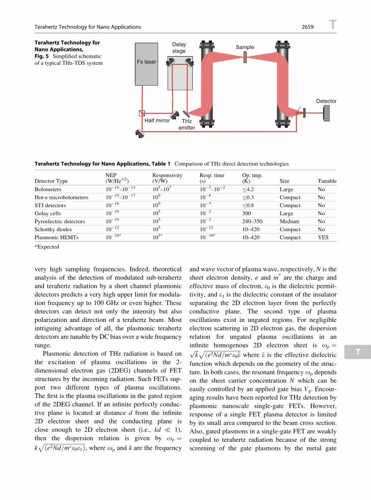
shown in Fig. 5, includes an ultrafast laser (e.g.,
Ti-Sapphire laser) which produces optical pulses in fs
duration. Each pulse is separated into two optical
paths. One path travel through a time delay stage and
hits the emitter such as a photoconductive antenna or
a nonlinear crystal in which the optical pulses are
converted into ultrashort electromagnetic pulses. The
generated EM pulses are focused onto the sample
under test and collimated again to be focused onto
the detector. The other part of the pulse is also deliv-
ered onto the detector directly. Amplitude of the
electromagnetic waves are measured by the detector
to calculate the change in the waveform due to the
sample. By changing delay time between the two
beams, it is possible to scan the THz pulse and
construct its electric field as a function of time.
Subsequently, a Fourier transform is used to extract
the frequency spectrum from the time-domain data.
Comparison of the waveforms with and without the
sample allows the estimation of the complex refractive
index of the material, which results other parameters,
such as the dielectric constant, conductivity and sur-
face impedance. Although they have been widely used
in research facilities, their size and complexity prevent
widespread deployment for out-of-lab applications.
On the other hand, CW imaging systems can be
passive, where the terahertz or sub-terahertz energy
analyzed is present in the environment or emitted by
the object itself (i.e., the human body), or active, where
the energy is supplied by a dedicated source. In active
systems, a major concern is the presently only limited
available terahertz sources. This limitation places
significant demands on detector capabilities. For CW
systems, two primary modalities exist for detection
of signals in the terahertz range. One involves the
reduction of the terahertz signal to sufficiently low
frequencies to allow amplification and signal
processing. This (heterodyne receiver) approach typi-
cally uses nonlinear diodes to mix the terahertz signal
with a local oscillator reference. Heterodyne detec-
tion imposes many restrictions on the system design
and makes it complex and expensive. These restric-
tions may be difficult or impossible to fulfill. The
second approach is direct detection, where the
terahertz signal impinging upon a detecting device
results in a measurable response. Available direct
detection technologies with key parameters are sum-
marized in Table 1.
As it is shown on Table 1, today the most sensitive
THz detectors are Golay cells, pyroelectric detectors,
bolometers, and Schottky diodes. However, they are
not portable, not tunable or, most of the time, are very
slow. Schottky diodes, for instance, can reach very low
noise equivalent power (NEP) and high responsivity at
millimeter waves. However, their responsivity drops
orders of magnitude (to <103 V/W) at frequencies
greater than 1 THz and they are not tunable.
Dyakonov and Shur proposed a novel idea of using
plasmonic resonances in the two-dimensional electron
gas (2DEG) for tunable emission and detection of
terahertz radiation, which are being explored and
proven experimentally, culminating in the recent dem-
onstration of resonant detection of the THz radiation at
room temperature. The theory [7, 8] predicts that such
detectors should have very high sensitivities (107 V/W
at 77 K and 104 V/W at 300 K). The plasmonic
detectors are capable for operating even at zero bias
current, thus minimizing shot noise and allowing
unprecedented sensitivity. GaN-based detectors
with noise equivalent power (NEP) smaller than
10�8 W/Hz1/2 have been demonstrated. This value is
slightly higher than for such commercial detectors as
Golay cell, pyroelectric detectors, and Schottky
diodes, with the potential advantage of operation at
Injector barrier×222
E43 = 15.6 meV
Collector barrier
432
1
2′3′
1′
hω
Terahertz Technology for Nano Applications, Fig. 4 Con-
duction band diagram of a diagonal design quantum cascade
laser with the lasing power of approximately 5 mW at 180 K.
1’ is the injector level from the preceding module. The figure
shows that the upper- and lower-state wave functions are local-
ized in separate wells with little spatial overlap and the radiative
transition is from 4 ! 3 (f ¼ E43/h ffi 3.8 THz). Therefore, this
scheme is called diagonal design (Adapted from [6])
T 2658 Terahertz Technology for Nano Applications
very high sampling frequencies. Indeed, theoretical
analysis of the detection of modulated sub-terahertz
and terahertz radiation by a short channel plasmonic
detectors predicts a very high upper limit for modula-
tion frequency up to 100 GHz or even higher. These
detectors can detect not only the intensity but also
polarization and direction of a terahertz beam. Most
intriguing advantage of all, the plasmonic terahertz
detectors are tunable by DC bias over a wide frequency
range.
Plasmonic detection of THz radiation is based on
the excitation of plasma oscillations in the 2-
dimensional electron gas (2DEG) channels of FET
structures by the incoming radiation. Such FETs sup-
port two different types of plasma oscillations.
The first is the plasma oscillations in the gated region
of the 2DEG channel. If an infinite perfectly conduc-
tive plane is located at distance d from the infinite
2D electron sheet and the conducting plane is
close enough to 2D electron sheet (i.e., kd � 1),
then the dispersion relation is given by op ¼kffiffiffiffiffiffiffiffiffiffiffiffiffiffiffiffiffiffiffiffiffiffiffiffiffiffiffiffiffiðe2Nd=m�e0e1Þ
p, where op and k are the frequency
and wave vector of plasma wave, respectively, N is the
sheet electron density, e and m* are the charge and
effective mass of electron, e0 is the dielectric permit-
tivity, and e1 is the dielectric constant of the insulatorseparating the 2D electron layer from the perfectly
conductive plane. The second type of plasma
oscillations exist in ungated regions. For negligible
electron scattering in 2D electron gas, the dispersion
relation for ungated plasma oscillations in an
infinite homogenous 2D electron sheet is op ¼ffiffiffik
p ffiffiffiffiffiffiffiffiffiffiffiffiffiffiffiffiffiffiffiffiffiffiffiffiffiffiðe2Nd=m�e0�ep
where �e is the effective dielectric
function which depends on the geometry of the struc-
ture. In both cases, the resonant frequency op depends
on the sheet carrier concentration N which can be
easily controlled by an applied gate bias Vg. Encour-
aging results have been reported for THz detection by
plasmonic nanoscale single-gate FETs. However,
response of a single FET plasma detector is limited
by its small area compared to the beam cross section.
Also, gated plasmons in a single-gate FET are weakly
coupled to terahertz radiation because of the strong
screening of the gate plasmons by the metal gate
Terahertz Technology for Nano Applications, Table 1 Comparison of THz direct detection technologies
Detector TypeNEP Responsivity Resp. time Op. tmp.
Size Tunable(W/Hz1/2) (V/W) (s) (K)
Bolometers 10�16–10�13 105–107 10�3–10�2 �4.2 Large No
Hot-e microbolometers 10�19–10�17 109 10�8 �0.3 Compact No
STJ detectors 10�16 109 10�3 �0.8 Compact No
Golay cells 10�10 105 10�2 300 Large No
Pyroelectric detectors 10�10 105 10�2 240–350 Medium No
Schottky diodes 10�12 103 10�12 10–420 Compact No
Plasmonic HEMTs 10�10* 103* 10�10* 10–420 Compact YES
*Expected
Delaystage
Sample
Fs laser
Half mirror THzemitter
Detector
Terahertz Technology forNano Applications,Fig. 5 Simplified schematic
of a typical THz-TDS system
Terahertz Technology for Nano Applications 2659 T
T

electrode and their vanishingly small net dipole
moment due to their acoustic nature. Coupling effi-
ciency can be greatly enhanced by utilizing multiple
gates (grating gate) on a common channel (Fig. 6a) or
multichannel FETs having an array of separate chan-
nels with combined intrinsic source and drain contacts
(Fig. 6b). Resonant coupling of THz radiation into the
plasmons in 2DEG of a single-channel multi-gate
plasmonic device have been demonstrated which
could be used for precise tuning by the applied gate
voltage (Fig. 6c).
THz Applications
Distinctive position of THz frequencies in the electro-
magnetic spectrum with their lower quantum energy
compared to IR and higher frequency compared to
MW range calls for many potential applications unique
to them. The former characteristic allows detection and
identification of substances based on their spectral
signatures due to molecular vibration and rotation,
while the latter one allows wide bandwidth for wire-
less communication. Indeed, spectroscopic analysis,
sensing, and imaging represent the major application
category of today’s THz technology. Near-field
imaging for subwavelength-scale small features is
a notably fast-advancing field in this category.
Communication, although still at infancy, is also
promising application for THz frequencies.
Spectroscopic Sensing and Imaging
The unique advantage of THz waves for many appli-
cations can be attributed to their low frequency (or low
quantum energy) compared to the commonly used
parts of the optical spectrum. The low energy of
terahertz photons can perhaps be better appreciated
when compared to average thermal energy, 1 THz
corresponds to just 4 meV, or about 1/6th of the energy
in one degree of freedom at 300 K. Therefore, terahertz
Multi-gate structure
Source
2DEG channel N1 N2 Substrate
Substrate
Drain
THz radiation
W L
E0
THz radiation
W LGate
Barrier
Source-and-drain contacts2DEG channels
Frequency (THz)
c
b
a
0.6
0.4
0.2
0.01.0 1.5 2.0 2.5
−5v−4v
−3v−2v
−1v0v
Tran
smis
sio
n (
a.u
.)– + +
+ + +– – –
–
Terahertz Technology for Nano Applications, Fig. 6 Sche-
matics of the plasmonic devices with (a) multiple gates (grating
gate) on a common channel, (b) multichannel FETs having an
array of separate channels with combined intrinsic source and
drain contacts, (c) transmission spectra of a AlGaN/GaN
single-channel multi-gate plasmonic device at different gate
voltages. The data shows the possibility of tunable THz detec-
tion. The inset shows the close-up SEM image of the gate
elements of the measured device (Adapted from [9])
T 2660 Terahertz Technology for Nano Applications

radiation is useful for studying very low-frequency
phenomena such as vibrations and rotations in mole-
cules and soft lattice vibrations in dielectrics. Since
materials, such as polymers, clothes, plastic, wood,
and soil are nearly transparent to terahertz rays, while
water, window-glass, and most metals are opaque;
many novel imaging applications are available with
T-rays. To date, THz waves have been used to read
letters in closed envelopes, to detect hidden explosives
and weaponry, pharmaceutical quality control, and to
detect tumors in breast and epidermal tissue.
THz frequencies are particularly important for
biosensing applications since numerous characteristic
vibrational modes of macromolecules like proteins and
DNA are located in this spectral range. This correspon-
dence opens up the possibility of label-free biosensing.
Although millimeter wave spectroscopy has been
known since the 1950s, the cost was prohibitive and
studies did not extend to large biological proteins such
as DNA. In 1995, Hu and Nuss demonstrated the first
THz imaging system based on THz-TDS which has
become the method of choice for demonstration of
many sensing and imaging applications [10]. Shortly
after, Woolard et al. proposed to use millimeter-THz
spectrocopy for detecting DNA mutagenesis. In this
first attempt, they successfully demonstrated the
lesion-induced vibrational modes in DNA observed
from 80 to 1,000 GHz. The observed modes were
associated with localized defects of the DNA polymers
[11]. Low-frequency collective vibrational modes of
lyophilized powder samples of calf thymus DNA,
bovine serum albumin (BSA), and collagen in the
0.06–2.00 THz frequency range have been studied,
showing that a large number of the low-frequency
collective modes for these systems are active in this
range. Further studies demonstrated the feasibility
of THz-TDS to (a) identify biomolecular species,
(b) identify the conformational state, and (c) identify
the mutation of biomolecules. The understanding of
conformational change and flexibility is particularly
critical for bioengineering of biomolecules for drug
discovery and therapeutic purposes. Transmission
spectra of the nucleobases (adenine, cytosine, guanine,
thymine) have also been measured to identify the
spectral signatures at THz frequencies (see Fig. 7).
In the security side of the THz sensing applica-
tions, absorption spectra of explosives and related
compounds (ERCs) by using THz-TDS has also
been measured. The obtained absorption spectra in
the range of 0.1–3 THz show that most of the ERCs
have THz fingerprints which are caused by both the
intramolecular and intermolecular vibrational modes
of these materials (Fig. 8). Since commonly used
nonpolar dielectric materials (e.g., fabric, leather)
are almost transparent in the THz range, THz finger-
prints makes THz technology a competitive technique
for detecting hidden explosives. In most of these
studies, the samples under investigation were either
simply deposited on a THz-transparent (e.g., polyeth-
ylene) substrate, placed in a cell consisting of the
same or, in rare cases, formed into durable free stand-
ing films.
100 Adenine 10%
50
0
100 Guanine 5%
5Frequency (THz)
4321
50
Tran
smitt
ance
(%
)Tr
ansm
ittan
ce (
%)
0
100 Cytosine 2%
50
0
100 Thymine 5%
5Frequency (THz)
4321
50
Tran
smitt
ance
(%
)Tr
ansm
ittan
ce (
%)
0
Terahertz Technology forNano Applications,Fig. 7 Transmission spectra
of the nucleobases (adenine,
cytosine, guanine, thymine) at
THz frequencies identify their
spectral signatures (After [12])
Terahertz Technology for Nano Applications 2661 T
T
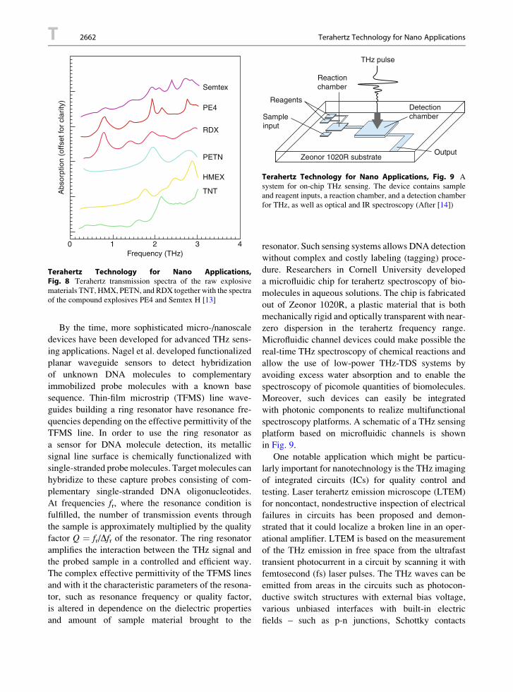
By the time, more sophisticated micro-/nanoscale
devices have been developed for advanced THz sens-
ing applications. Nagel et al. developed functionalizedplanar waveguide sensors to detect hybridization
of unknown DNA molecules to complementary
immobilized probe molecules with a known base
sequence. Thin-film microstrip (TFMS) line wave-
guides building a ring resonator have resonance fre-
quencies depending on the effective permittivity of the
TFMS line. In order to use the ring resonator as
a sensor for DNA molecule detection, its metallic
signal line surface is chemically functionalized with
single-stranded probe molecules. Target molecules can
hybridize to these capture probes consisting of com-
plementary single-stranded DNA oligonucleotides.
At frequencies fr, where the resonance condition is
fulfilled, the number of transmission events through
the sample is approximately multiplied by the quality
factor Q ¼ fr/Dfr of the resonator. The ring resonator
amplifies the interaction between the THz signal and
the probed sample in a controlled and efficient way.
The complex effective permittivity of the TFMS lines
and with it the characteristic parameters of the resona-
tor, such as resonance frequency or quality factor,
is altered in dependence on the dielectric properties
and amount of sample material brought to the
resonator. Such sensing systems allows DNA detection
without complex and costly labeling (tagging) proce-
dure. Researchers in Cornell University developed
a microfluidic chip for terahertz spectroscopy of bio-
molecules in aqueous solutions. The chip is fabricated
out of Zeonor 1020R, a plastic material that is both
mechanically rigid and optically transparent with near-
zero dispersion in the terahertz frequency range.
Microfluidic channel devices could make possible the
real-time THz spectroscopy of chemical reactions and
allow the use of low-power THz-TDS systems by
avoiding excess water absorption and to enable the
spectroscopy of picomole quantities of biomolecules.
Moreover, such devices can easily be integrated
with photonic components to realize multifunctional
spectroscopy platforms. A schematic of a THz sensing
platform based on microfluidic channels is shown
in Fig. 9.
One notable application which might be particu-
larly important for nanotechnology is the THz imaging
of integrated circuits (ICs) for quality control and
testing. Laser terahertz emission microscope (LTEM)
for noncontact, nondestructive inspection of electrical
failures in circuits has been proposed and demon-
strated that it could localize a broken line in an oper-
ational amplifier. LTEM is based on the measurement
of the THz emission in free space from the ultrafast
transient photocurrent in a circuit by scanning it with
femtosecond (fs) laser pulses. The THz waves can be
emitted from areas in the circuits such as photocon-
ductive switch structures with external bias voltage,
various unbiased interfaces with built-in electric
fields – such as p-n junctions, Schottky contacts
TNT
Semtex
PE4
RDX
PETN
HMEX
0 1 2 3 4Frequency (THz)
Abs
orpt
ion
(offs
et fo
r cl
arity
)
Terahertz Technology for Nano Applications,Fig. 8 Terahertz transmission spectra of the raw explosive
materials TNT, HMX, PETN, and RDX together with the spectra
of the compound explosives PE4 and Semtex H [13]
OutputZeonor 1020R substrate
Reactionchamber
Reagents
Sampleinput
THz pulse
Detectionchamber
Terahertz Technology for Nano Applications, Fig. 9 A
system for on-chip THz sensing. The device contains sample
and reagent inputs, a reaction chamber, and a detection chamber
for THz, as well as optical and IR spectroscopy (After [14])
T 2662 Terahertz Technology for Nano Applications

(metal/semiconductor interfaces) – or just the surface
of semiconductor. The THz emission amplitude is
proportional to the local electric field in the photo-
excited area. By comparing the THz emission images
of a normal and damaged chip, the abnormal electrical
field resulting from an electrical failure in the circuit
can be visualized (Fig. 10). However, the spatial reso-
lution of LTEMwas strongly affected by the long focal
length of the focusing lens and the aperture size in the
system, limiting it to about 20 mm. Therefore,
noncontact testing of ICs using THz radiation required
near-field imaging techniques which will be discussed
in the next section.
THz Near-Field Imaging and THz Microscopy
Low-energy photons of THz radiation make a rich
variety of light-matter interactions possible by exciting
molecular vibrations and phonons as well as plasmons
and electrons of nonmetallic conductors. Therefore,
T-rays offer new ways for material and device charac-
terization. However, diffraction limits the spatial res-
olution to the order of wavelength and prevents the use
of THz waves for imaging beyond �100 mm.
Conventional imaging methods cannot be employed
for THz mapping of micro- or nanoelectronic devices,
low-dimensional semiconductor nanostructures, cellu-
lar entities, or single molecules. This problem can be
circumvented by invoking the near-field scanning opti-
cal microscopy technique for THz imaging applica-
tions. One way to overcome the diffraction limit is to
limit the detection area with an aperture. It has been
shown that using a detector with an integrated aperture,
near-field images can be made with a spatial resolution
determined by the aperture size, and not by the THz
wavelength. This method, however, suffered from
microfabrication complexity and waveguide effects
which lead to strong attenuation for long wavelength
components. A widely explored alternative method is
the use of sharp metal tips as local field enhancers. The
sharp metal tip is held in close contact to the sample
under study, while light is scattered by the tip. Acting
as antennas, the wires capture incident THz waves and
convert them into strongly confined near fields at the
wire tip apex which has submicrometer dimensions.
When this confined field becomes modified by
a close-by scanned sample, the scattered radiation
5 μm
50
45
40
35
30
25
20
15
10
5
0−1.0 −0.5 0.0 1.00.5
THz amplitude (arb. units)
Pos
ition
(μm
)
−1
1a b
Terahertz Technology for Nano Applications, Fig. 10 (a)The THz emission image an LSI 8-bit microprocessor chip. The
red and blue regions indicate THz emissions with positive and
negative amplitudes, respectively, which correspond to the
direction of the electric field. (b) The magnified THz emission
image of the area indicated by the white square in Fig. 10a. The
inset shows the cross-sectional distribution of the THz emission
image at the dotted line (After [15])
Terahertz Technology for Nano Applications 2663 T
T

carries information on the local dielectric properties
of the sample. This apertureless near-field imaging,
which was originally developed at visible and
mid-infrared wavelengths, has recently been demon-
strated at terahertz wavelengths. THz images with
a subwavelength resolution can be obtained by record-
ing the scattered radiation by a distant THz receiver.
A big advantage of this imaging technique is that it
does not suffer from a waveguide cutoff, which limits
the resolution in aperture techniques. Attempts of
realizing such THz-scattering near-field optical
microscopy (THz-SNOM), however, suffer from
weak signals and faint material contrasts owing to
strong background scattering.
In the first demonstration of THz near-field imaging
at THz frequencies, Hunsche et al. used ultrashort,
broadband pulses which were focused into a tapered
metal tip with a small exit aperture and scanned
a sample in the near field of this aperture. Their method
allowed spatial resolution better than l/4 for the
corresponding average wavelength of 220 mm [16].
Huber et al. demonstrated high-resolution THz near-
field microscopy using the experimental setup shown
in Fig. 11 [17]. The THz signal was incident through
a parabolic mirror with an angle to allow total internal
reflection over the sample surface. On top of the sam-
ple, a cantilever of 20 mm length holding a metallic tip
of 30 nm radius vibrated to modulate the incident wave
in an On and Off manner. The cantilever mechanically
oscillated at the mechanical resonance frequency of
35 kHz. A Michelson interferometer detector and
hot electron bolometer were used to measure
backscattered THz radiation. This technique allowed
30–150 nm spatial resolution imaging, corresponding
to l/4,000 for 2.54 THz. Moreover, near-field THz
contrast between materials with different dielectric
properties allowed imaging of a polished cut through
nanoscale transistor structure and simultaneous recog-
nition of materials and concentration of mobile carriers
in the range of 1016–1019 cm�3. Since the spatial res-
olution of 40 nm infers that the volume probed by the
THz near-field is about (40 nm)3, it can be concluded
that an average of less than 100 electrons in the probed
volume suffices to evoke significant THz contrast. This
opens the possibility of THz studies of single electrons
by improving the used setup and, in conjunction with
ultrafast techniques, even their dynamics. The reported
results are encouraging to use THz near-field micros-
copy for studying other charged particles and quasi-
particles in condensed matter, for example, in
superconductors, low-dimensional electron systems,
or conducting biopolymers, which possess intrinsic
excitations at THz quantum energies and thus should
exhibit resonantly enhanced THz contrast (Fig. 12).
THz Communication
T-rays are very attractive for communication applica-
tions for the large bandwidth at these frequencies
which could provide very high data transmission
rates. Moreover, frequencies above 300 GHz are cur-
rently not allocated by the Federal Communications
Commission. On the down side, strong atmospheric
absorption due to the water vapor together with the
low available power of the current THz sources
limits the range of communication. A 10 mW source
and 1 pW detection sensitivity would be required for
1 km communication range considering the typical
attenuation rate of�100 dB/km rate in the atmospheric
absorption windows (Fig. 13).
The strong atmospheric attenuation, however, does
not pose a real threat for a number of communication
applications. Space communication, for instance, can
benefit from the high data transmission rates and
smaller antenna size required for THz frequencies
which would make possible the development of
smaller, lighter therefore satellites with longer life-
time. Large bandwidth of THz frequencies can also
be used to for short-range indoor communication
exceeding Gigabit/s transmission rates. Rayleigh scat-
tering of electromagnetic radiation is many orders
of magnitude less for THz wavelengths than for the
alternative infrared frequencies.
One unique and promising potential for THz
frequencies is the on-chip and communication, espe-
cially systems-on-chip (SoC) applications. With the
Bolometer
c.w. THz laser
MMirror
Beam-splitter
Parabolicmirror
Ω
Pie
zoTerahertz Technology for Nano Applications,Fig. 11 Schematic of apertureless THz scanning near-field
optical microscope (THz-SNOM) (After [17])
T 2664 Terahertz Technology for Nano Applications

ever-increasing complexity of integrated circuits,
larger and larger number of functional and storage
cores are squeezed into a single die. Extrapolating
from the current CMOS scaling trends, conventional
on-chip interconnect technologies have been projected
to reach their limits to meet the performance needs
of the next-generation multi-core and SoC systems.
Interconnect delays do not scale as well as local
wires with respect to gate delays, and global intercon-
nects have an increasing impact on the performance of
overall SoCs. A radical alternative to the existing
metal/dielectric interconnect infrastructures is to use
transmission of signals via wireless interconnects.
On-chip wireless interconnects were demonstrated
first for clock signal distribution at 15 GHz carrier
frequency [19]. If the THz frequencies are employed
for on-chip communication, corresponding antenna
sizes decrease occupying much less chip real estate.
Nanowires and carbon nanotubes (CNTs) can serve as
antenna structures in such applications. CNT bundles
are predicted to enhance performance of antenna mod-
ules by up to 40 dB in radiation efficiency and provide
SiO2
SiO2
poly-Si SiN
NiSi
a b c
Gate
Source Drain
Si
TEM IR THz
100 nm
100 nm
200 nm
300 nm
0.5 1.0
Norm. THz signal
40 nm
Terahertz Technology for Nano Applications, Fig. 12 (a)TEM image of a single transistor. The highly doped regions
below the source and drain NiSi contacts are marked by dashed
yellow lines. (b) Infrared image of the single transistor 12a (l�11 mm). (c) High-resolution THz image of the single showing all
essential parts of the transistor: source, drain, and gate. The THz
profile extracted along the dashed white line (averaged over
a width of 12 nm and normalized to the signal obtained on the
metallic NiSi gate contact) allows the estimation of a spatial
resolution of about 40 nm, from the strong signal change at the
SiO2/SiN/NiSi transition [17]
1000000
100000
10000
1000
100
10
1
0.10 0.2 0.4 0.6 0.8 1.0 1.2 1.4 1.6 1.8 2.0
Window of 1-dB loss for R = 10 m
Frequency (THz)
Atte
nuat
ion
(dB
/km
)
Terahertz Technology forNano Applications,Fig. 13 Atmospheric
attenuation in the THz
frequency range [18]
Terahertz Technology for Nano Applications 2665 T
T

excellent directional properties in far field patterns and
can achieve a bandwidth of 500 GHz and hence can
achieve much higher data rates (Fig. 14).
Cross-References
▶Biosensors
▶Nanostructure Field Effect Transistor Biosensors
Further Reading
1. Tonouchi, M.: Cutting-edge terahertz technology. Nat. Pho-
tonics 1, 97–105 (2007)
2. Diduck, Q., Irie, H., Margala, M.: A room temperature
ballistic deflection transistor for high performance applica-
tions. Int. J. High Speed Electron. Syst. 19, 23–31 (2009)
3. El Fatimy, A., Dyakonova, N., Meziani, Y., Otsuji, T.,
Knap, W., Vandenbrouk, S., Madjour, K., Theron, D.,
Gaquiere, C., Poisson, M.A., Delage, S., Prystawko, P.,
Skierbiszewski, C.: AlGaN/GaN high electron mobility
transistors as a voltage-tunable room temperature terahertz
sources. J. Appl. Phys. 107, 024504 (2010)
4. Dragoman, D., Dragoman, M.: Terahertz fields and applica-
tions. Prog. Quantum Electron. 28, 1–66 (2004)
5. Kohler, R., Tredicucci, A., Beltram, F., Beere, H.E.,
Linfield, E.H., Gilles Davies, A., Ritchie, D.A., Iotti, R.C.,
Rossi, F.: Terahertz semiconductor-heterostructure laser.
Nature 417, 156–159 (2002)
6. Kumar, S., Hu, Q., Reno, J.L.: 186 K operation of terahertz
quantum-cascade lasers based on a diagonal design. Appl.
Phys. Lett. 94, 131105 (2009)
7. Dyakonov, M.I., Shur, M.S.: Shallow water analogy for
a ballistic field effect transistor: new mechanism of plasma
wave generation by dc current. Phys. Rev. Lett. 71, 2465(1993)
8. Dyakonov, M.I., Shur, M.S.: Detection, mixing, and fre-
quency multiplication of terahertz radiation by two dimen-
sional electronic fluid. IEEE Trans. Electron Devices 43,380 (1996)
9. Muravjov, A.V., Veksler, D.B., Popov, V.V., Polischuk, O.
V., Pala, N., Hu, X., Gaska, R., Saxena, H., Peale, R.E.,
Shur, M.S.: Temperature dependence of plasmonic terahertz
absorption in grating-gate GaN HEMT structures. Appl.
Phys. Lett. 96, 042105 (2010)
10. Hu, B.B., Nuss, M.C.: Imaging with terahertz waves. Opt.
Lett. 20, 1716–1718 (1995)
11. Woolard, D.L., Koscica, T., Rhodes, D.L., Cuj, H.L.,
Pastore, R.A., Jensen, J.O., Jensen, J.L., Loerop, W.R.,
Jacobsen, R.H., Mittleman, D., Nuss, M.C.: Millimeter
wave-induced vibrational modes in DNA as a possible alter-
native to animal tests to probe for carcinogenic mutations. J.
Appl. Toxicol. 17, 243–246 (1997)
12. Nishizawa, J.: Development of THz wave oscillation and its
application to molecular sciences. Proc. Jpn. Acad. B 80,74 (2004)
13. Kemp, M.C., Taday, P.F., Cole, B.E., Cluff, J.A., Fitzgerald,
A.J., Tribe, W.R.: Security applications of terahertz tech-
nology. In: Hwu, R.J., Woolard, D.L. (eds.) Terahertz for
Military and Security Applications, vol. 5070, pp. 44–52.
SPIE, Bellingham (2003)
14. George, P.A., Hui, W., Rana, F., Hawkins, B.G., Smith, A.E.,
Kirby, B.J.: Microfluidic devices for terahertz spectroscopy
of biomolecules. Opt. Express 16, 1577 (2008)15. Yamashita, M., Kawase, K., Otani, C.: Imaging of large-
scale integrated circuits using laser terahertz emission
microscopy. Opt. Express 13, 115 (2005)
16. Hunsche, S., Koch, M., Brener, I., Nuss, M.C.: THz near-
field imaging. Opt. Commun. 150, 22 (1998)
17. Huber, A.J., Keilmann, F., Wittborn, J., Aizpurua, J.,
Hillenbrand, R.: Terahertz near-field nanoscopy of mobile
carriers in single semiconductor Nanodevices. Nano Lett. 8,3766–3770 (2008)
RX RX RX RX
RX RX RX RX
RX RX RX RX
RX
RX receiver
RX RX RX
TX
IC edge
TX transmitter
Receiving antennas (PC Board / MCM)
Integratedcircuits
transmittedclock signal
Transmittingantenna (with
parabolic reflector)
Zs
a bTerahertz Technology forNano Applications,Fig. 14 Conceptual system
illustrations of (a) intra-chipand (b) inter-chip wireless
interconnect systems for clock
signal distribution (After [19])
T 2666 Terahertz Technology for Nano Applications

18. Fitch, M.J., Osiander, R.: Terahertz waves for communica-
tions and sensing. Johns Hopkins APL Tech. Dig. 25,348 (2004)
19. Floyd, B.A., Hung, C.M., Kenneth, K.O.: Intra-chip wire-
less interconnect for clock distribution implemented with
integrated antennas, receivers and transmitters. IEEE J.
Solid-State Circuits 37, 543 (2002)
Theoretical Elasticity
▶ Superelasticity and the Shape Memory Effect
Theory of Artificial ElectromagneticMaterials
▶Theory of Optical Metamaterials
Theory of Optical Metamaterials
Carsten Rockstuhl, Christoph Menzel, Stefan M€uhlig
and Falk Lederer
Institute of Condensed Matter Theory and Solid State
Optics, Abbe Center of Photonics, Friedrich-Schiller-
Universit€at Jena, Jena, Germany
Synonyms
Composite materials; Effective media; Left-handed
materials; Theory of artificial electromagnetic materials
Definition
Optical metamaterials can be understood as artificial
media consisting of suitably assembled micro- or nano-
structured materials such as dielectrics or metals and
acquiring their essential properties from the structure
rather than from the underlyingmaterial. The purpose of
metamaterials is to affect the characteristics of light
propagation in a manner inaccessible with natural avail-
able media. Their theoretical description evokes various
concepts which are outlined in this essay.
Introduction
Optical metamaterials (MMs) can be understood as
artificial media consisting of suitably assembled
micro- or nanostructured materials such as dielectrics
or metals [1–3] and acquiring their essential properties
from the structure rather than from the underlying
material. The purpose of MMs is to affect the charac-
teristics of light propagation in a manner inaccessible
with natural available media; hence the term material
was linked with the prefix meta, being derived from
Greek and literally meaning beyond or after. This
rather generic and broad definition comprises many
kinds of structured materials. Examples thereof
would be photonic crystals or plasmonic structures
[4, 5]. In a stricter sense, as the definition is further
refined here, MMs are thought to be made from unit
cells a few times or much smaller than the wavelengths
in the spectral domain of interest. Here restriction is
made specifically to the latter case where the propa-
gating light does not probe for the fine details of the
unit cells [6]. Its propagation can rather be fully under-
stood by replacing the complex-shaped MM with
a homogenous medium to which effective properties
are assigned [7]. In the alternative case where the
unit cell is only a few times less than the relevant
wavelength, that is, the metamaterials represent a
mesoscopic system, nonlocal effects come into play
and the assignment of both an effective permittivity
and permeability ceases to be meaningful. Alternative
approaches for describing light propagation have to be
used which are beyond the scope of this entry.
Depending on which approach is chosen to discuss
MMs, the innovation comes with the deliberation from
restrictions imposed by nature. The linear optical prop-
erties of natural materials at optical frequencies are
entirely described by considering the permittivity
function only, that is, a complex frequency-dependent
function characterizing the response of matter to an
electric field. The permeability function, which char-
acterizes the response of matter to a magnetic field, can
be safely disregarded since it marginally deviates from
that of vacuum. For any frequency considered both
permeability and permittivity represent material
parameters and are linked to wave parameters, as for
example, the wave vector or the refractive index, by
the dispersion relation of the normal- or eigenmodes
which is of pivotal importance to describe the propa-
gation of electromagnetic fields in any structure. These
Theory of Optical Metamaterials 2667 T
T


