
www.sciencemag.org/cgi/content/full/1150878/DC1
Supporting Online Material for
Chemically Derived, Ultrasmooth Graphene Nanoribbon Semiconductors
Xiaolin Li, Xinran Wang, Li Zhang, Sangwon Lee, Hongjie Dai*
*To whom correspondence should be addressed. E-mail: [email protected]
Published 24 January 2008 on Science Express
DOI: 10.1126/science.1150878
This PDF file includes:
Materials and Methods Figs. S1 to S7 References

S 1
Chemically Derived, Ultra-Smooth Graphene Nano-Ribbon Semiconductors
Xiaolin Li†, Xinran Wang†, Li Zhang, Sangwon Lee and Hongjie Dai*
Department of Chemistry and Laboratory for Advanced Materials, Stanford University,
Stanford, CA 94305, USA
Supporting Online Materials Content:
(1) Method of graphene nanoribbon (GNR) making.
(2) Elemental analysis and spectroscopic analysis.
(3) Characterization of graphene ribbon width and thickness (number of layers) by
AFM.
(4) Making Graphene nanoribbon FETs.
(5) Comparison with theoretical results of graphene nano-ribbon bandgap Eg versus
width.
(6) Transmission electron microscopy (TEM) characterization
(7) Raman spectroscopic characterization of graphene samples
(8) Electrical transport properties of GNRs wider than 10nm
(1) Method of graphene nanoribbon (GNR) making.
Our GNR making method started by exfoliating expandable graphite (160-50N of
Grafguard Inc., made by intercalating ~350 micron scale graphite flakes with sulfuric
acid and nitric acid) at 1000°C in forming gas for 1 min, sonicating the resulting
exfolicated material in a 1,2-dichloroethane (DCE) solution of poly(m-
phenylenevinylene-co-2,5-dioctoxy-p-phenylenevinylene) (PmPV) (0.1mg/mL) to
disperse and break up the graphenes into small graphene sheets and GNRs, and

S 2
centrifuging the suspension to retain the GNRs (together with small sheets) in the
supernatant and remove other materials including large graphene pieces and not fully
exfoliated graphite flakes. Note that only ~ 0.5% of the starting material was retained in
the supernatant, which suggests that the majority of the material remained in many layer
structures that were heavy and removed by centrifugation. The retained graphene in the
suspension were comprised of lighter single and few-layer graphene in ribbon and sheet
forms. The number of ribbons was sufficient for depositing onto substrates for
characterizations by microscopy and electrical transport experiments. The high
temperature exfoliation step was a crucial step to the preparation of graphene
nanoribbons. It resulted in many thin graphite sheets including a small percentage of
single and few-layer graphene. This was indicated by that after exfoliation, the volume of
the exfoliated graphite (Fig. S1B) was hundreds of times higher than before exfoliation
(Fig. S1A). The BET surface area of such exfoliated graphite was on the order of
~60m2/g (1), much higher than before exfoliation but still far below that of single-layer
graphene. Thus, much room still exists to better exfoliate graphite and increase the yield
of single and few-layers by chemical methods.
The use of PmPV and DCE were also key to the preparation of GNR suspension,
similar to suspending carbon nanotubes (2, 3). We tried various other solvents and
coating molecules and the combination of PmPV/DCE was the best for suspending
graphene. The suspensions were made as follows: The exfoliated graphite (~1mg) was
bath-sonicated with PmPV (~1mg) in 10mL DCE for 30mins to form a uniform
dispersion (Fig. S1C). The suspension was then centrifuged at 15k rpm (round per
1 J. H. Han, K. W. Cho, K. -H. Lee, H. Kim, Carbon 36, 1801 (1998.) 2 J. F. Stoddart, et al., Angew. Chem. Int. Ed. 40, 1721 (2001). 3 X. L. Li, et al, J. Am. Chem. Soc. 129, 4890 (2007).
S 3
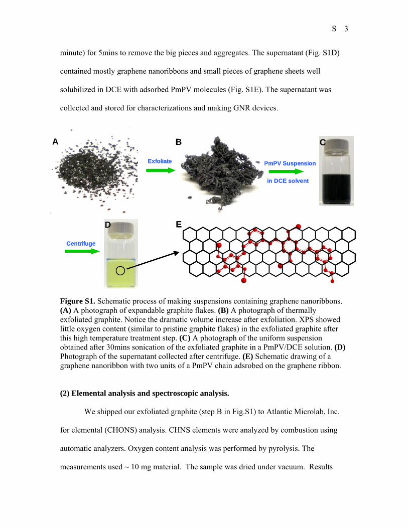
minute) for 5mins to remove the big pieces and aggregates. The supernatant (Fig. S1D)
contained mostly graphene nanoribbons and small pieces of graphene sheets well
solubilized in DCE with adsorbed PmPV molecules (Fig. S1E). The supernatant was
collected and stored for characterizations and making GNR devices.
Exfoliate PmPV Suspension
in DCE solvent
Centrifuge
A B C
D E
Exfoliate PmPV Suspension
in DCE solvent
Centrifuge
A B C
D E
Figure S1. Schematic process of making suspensions containing graphene nanoribbons. (A) A photograph of expandable graphite flakes. (B) A photograph of thermally exfoliated graphite. Notice the dramatic volume increase after exfoliation. XPS showed little oxygen content (similar to pristine graphite flakes) in the exfoliated graphite after this high temperature treatment step. (C) A photograph of the uniform suspension obtained after 30mins sonication of the exfoliated graphite in a PmPV/DCE solution. (D) Photograph of the supernatant collected after centrifuge. (E) Schematic drawing of a graphene nanoribbon with two units of a PmPV chain adsrobed on the graphene ribbon.
(2) Elemental analysis and spectroscopic analysis.
We shipped our exfoliated graphite (step B in Fig.S1) to Atlantic Microlab, Inc.
for elemental (CHONS) analysis. CHNS elements were analyzed by combustion using
automatic analyzers. Oxygen content analysis was performed by pyrolysis. The
measurements used ~ 10 mg material. The sample was dried under vacuum. Results

S 4
showed that the exfoliated graphite contained 95.7% C, 0.31% of O, 0.86% S, and the
HN elements were below the detection limit of 0.3%. The remaining uncounted few
percent of materials were attributed to impurities most likely existed in the original
expandable graphite. Currently, we do not have ~10mg of ribbon samples (step D in
Fig.S1) for similar analysis.
We carried out X-ray photoelectron spectroscopy (XPS) analysis of our ribbon
sample. Sample preparation involved depositing materials from step D of Fig.S1 onto a
silicon substrate by repeated drop-drying. The large amount of deposits was then
analyzed by XPS (SSI S-Probe Monochromatized XPS Spectrometer, which uses Al (Kα)
radiation as a probe. Analysis spot size is 150 micron by 800 micron.). For comparison,
we also took XPS spectra of a pristine highly oriented pyrolytic graphite HOPG sample.
Fig.S2 shows that the C1s peak structure of our ribbon sample was similar to that of
pristine HOPG, without significant signals corresponding to C-O species. This suggests
the high pristine nature of our ribbon samples without excessive covalent chemical
functionalization as in the case of graphite oxide (4). For graphite oxide known to be
heavily functionalized covalently, high signals in the higher binding energy region
corresponding to C-O bonding was observed in XPS (4), in strong contrast to our ribbon
samples and pristine HOPG.
4 S. Stankovich, R. D. Piner, X. Q. Chen, N. Q. Wu, S. B. T. Nguyen, R. S. Ruoff, J. Mater. Chem. 16, 155 (2006).

S 5
275 280 285 2900
500
1000
1500
2000
2500
Cou
nts
(a. u
.)
Binding energy (eV)
GNR HOPG
Figure S2. The C1s XPS spectra recorded with our graphene nanoribbon deposits on a substrate and vacuum annealed at 600°C (black curve) and a pristine HOPG crystal (red curve) respectively.
(3) Characterization of graphene ribbon width and thickness (number of layers) by
AFM.
Care was taken to measure the ribbon width accurately using AFM since the
radius of our Si AFM tips (Veeco multi75) was around 10-20nm. To count for the tip size
effect, we used diameter-separated Hipco SWNT samples with very narrow diameter
distribution around 1.1nm to calibrate the AFM tip. We took high quality images of the
SWNTs and measured the apparent widths to glean tip width (typically ~ 6-7nm), which
was then corrected from the apparent width of GNRs measured by AFM. From > 100
ribbons we imaged in this work, we often observed a few discrete heights, namely 1.1nm,
1.5nm, 1.9nm, and never observed a GNR or other shaped graphene with height less than
1nm. Thicker ribbons were also observed but not used for further studies such as
transport measurements. We assigned the GNRs with height ~1.1nm, ~1.5nm, and
~1.9nm to be 1, 2, 3-layer GNRs, respectively. This assignment was also consistent with

S 6
the reported AFM results on few-layer graphene sheets, where the single layer graphene
is always ~1nm (5, 6), possibly due to different attraction force between AFM tips and
graphene as compared to SiO2 and non-perfect interface between graphene and SiO2.
Below we presented the raw height profile data (Fig. S3) for several 1-layer, 2-layer and
3-layer ribbons in Fig. 1 and Fig. 2 of the main text.
1.059 nm1.059 nm
1.023 nm1.023 nm
1.031 nm1.031 nm
A
C
B
5 K. S. Novoselov, A. K. Geim, S.V. Morozov, D. Jiang, Y. Zhang, S. V. Dubonos, I. V. Grigorieva, & A. A. Firsov, Science 306, 666 (2004). 6 A. Gupta, G. Chen, P. Joshi, S. Tadigadapa, P. C. Eklund, Nano Lett. 6, 2667 (2006).

S 7
1.515 nm1.515 nm
1.512 nm1.512 nm
1.503 nm1.503 nm
1.832 nm1.832 nm
D
E
F
G

S 8
H
I
1.870 nm1.870 nm
1.908 nm1.908 nm
Figure S3. Topographic height profiles of several ribbons in Fig. 1 and Fig. 2 of main text. In each row, the left image is the same as shown in Fig.1 or Fig.2 of the main text. The middle image is a zoom-in image, with which topographic analysis is done. (A), (B), and (C) are left panel of Fig. 1B, right panel of Fig. 1D, and Fig. 2B of the main text respectively. They are single layer graphene with the height of about ~1.0nm. (D), (E), and (F) are middle panel of Fig. 1B, left panel of Fig. 1F, and Fig. 2A of the main text respectively. These are two-layer GNRs with the height of ~1.5nm. (G), (H), and (I) are left panel of Fig. 1C, middle panel of Fig. 1D, and Fig. 2D of the main text respectively. These are three-layer graphene with the height of ~1.9nm.
We imaged our GNRs by using single-walled carbon nanotube AFM tips (7).
Such tips were comprised of a single or small bundle of nanotubes (2-5nm in diameter)
and gave higher lateral resolution than conventional Si tips. Indeed, we observed that
AFM with nanotube tips gave narrower apparent width than conventional tips by ~4nm.
Fig.S4 shows an example of a sub-10nm GNR exhibiting apparent width of 12nm and
7 E. Yenilmez, Q. Wang, R. J. Chen, D. W. Wang, H. J. Dai, Appl. Phys. Lett. 80, 2225 (2002).

S 9
8nm imaged by Si tip and nanotube tip respectively. The nanotube tips still have a finite
size, which will need to be taken into account in order to measure the widths of GNRs.
A B
C

S 10
D
Figure S4. (A) An AFM image of a sub-10nm GNR imaged by a Si tip, (B) AFM image of the same ribbon imaged by a carbon nanotube tip. (C)&(D) Topographic line-cut measurements for the two images in (A) and (B), showing an apparent width of the ribbon of ~12nm (Si tip) and ~8nm (nanotube tip) respectively.
Optical microscopy has been used to determine the thickness and layer number of
large graphene sheets in the literature. The narrow GNRs in the current work were
difficult to resolve and identify under a typical optical microscope. Raman spectra have
been well used before to determine the number of layers of big graphene sheets. However,
the Raman spectroscopic properties of GNRs with narrow widths are not known and
require systematic investigation by experiments and theory (8). The Raman spectra of
GNRs may differ significantly from large graphene with new features due to quantum
confinement of phonon and electron (6). Systematic Raman spectroscopic investigation
of our GNRs is ongoing.
(4) Making Graphene nanoribbon FETs.
GNRs were deposited onto 300nm SiO2/p++ Si substrate with arrays of pre-
8 A. C. Ferrari, Solid State Commun. 143, 47 (2007).

S 11
deposited metal markers (2nm Ti/20nm Au) by soaking the substrate in the graphene
suspension in PmPV/DCE solution for 20min, rinsing with isopropanol and blow-dry
with argon. The chip was calcined in air at 400°C to burn away PmPV on the GNRs and
annealed in vacuum at 600°C to further clean the surface. Tapping mode AFM was then
used to locate ribbons and record relative locations to the pre-fabricated markers. S/D
electrode pattern was then designed for electrically contacting the GNRs, which was
carried out by electron beam lithography, 20nm Pd metal deposition and liftoff. The
devices were then annealed in 1000 sccm argon at 220°C for 15 min to improve contact
quality. We took the AFM image of GNRs in our devices immediately after annealing to
avoid contamination of graphene due to absorption of various molecules. After AFM, we
carried out electrical characterizations of our devices using a semiconductor analyzer
(Agilent 4156C, sensitivity ~10fA) to record transfer Ids vs. Vgs and Ids-Vds curves for the
graphene devices.
(5) Comparison with theoretical results of graphene nano-ribbon bandgap Eg versus
width w.
In Fig. 4B of main text, we plot first-principles based results of Eg versus w from
Ref. 7. Blue, orange and purple lines denote arm-chair edged GNRs with dimer lines
Na=3p, 3p+1 and 3p+2 (p is integer) across the ribbons respectively. The ribbon width is
cca a
Nw −
−= *
2)1(3
, where ~0.142nm is carbon-carbon bond length. The
bandgaps are
cca −
13sin
138 20
33, ++−Δ=
pp
ptE ppg
πδ (1)
23)1(sin
238 20
1313, ++
++Δ= ++ p
pp
tE ppgπδ (2)

S 12
120
2323, +−Δ= ++ p
tE ppg
δ (3)
where ⎟⎟⎠
⎞⎜⎜⎝
⎛−
+=Δ 2
13cos43
0
pptpπ , ⎟⎟
⎠
⎞⎜⎜⎝
⎛++
−=Δ +23)1(cos4213
0
pptp
π , , t=2.7eV and 0230 =Δ +p
12.0=δ . The green line in Fig. 4b denotes calculate bandgaps for zig-zag edged GNRs,
for which the equation is
15)(
33.9)(+Α
=w
eVE zigzagg . (4)
(6) Transmission electron microscopy (TEM) characterization
We characterized our solution phase derived graphene by a Philips CM20
transmission electron microscope (TEM) at an accelerating voltage of 200kV. The TEM
samples were prepared by drying a droplet of the graphene suspensions on a lacey carbon
grid. We observed many ribbon structures in the TEM with various widths and lengths.
Fig.S5 below shows a GNR with varying widths from about ~20nm to ~10nm along the
ribbon length (Fig.S5A). We recorded electron diffraction (ED) patterns of graphene over
many areas on the TEM gird and clearly observed hexagonal diffraction patterns
corresponding to graphene (Fig. S5C). Note that no carbon nanotubes were observed
through our TEM studies of graphene materials in our suspensions.

S 13
C
BA
C
BA
Figure S5. TEM and electron diffraction studies of graphene nanoribbon samples. (A) A TEM image showing a graphene nano-ribbon (~1 micron long) with width changing from about ~20nm to slightly below 10nm. (B) A zoom-in view of the ribbon in the marked region of (A). Notice the very smooth edges of the GNR. (C) A typical electron diffraction pattern of recorder for the graphene sample.
(7) Raman spectroscopic characterization of graphene samples
We used surface enhanced Raman to characterize graphene materials deposited on
Au coated substrates, using a Renishaw micro-Raman instrument with an excitation laser
wavelength of 785 nm and a laser spot size of about 2 microns. Samples for Raman
measurements were prepared by drying droplets of the graphene ribbon suspension onto
S 14
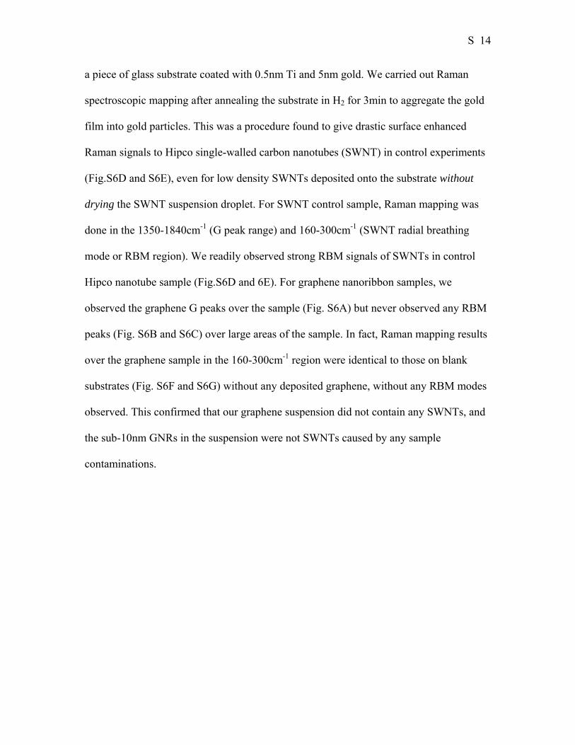
a piece of glass substrate coated with 0.5nm Ti and 5nm gold. We carried out Raman
spectroscopic mapping after annealing the substrate in H2 for 3min to aggregate the gold
film into gold particles. This was a procedure found to give drastic surface enhanced
Raman signals to Hipco single-walled carbon nanotubes (SWNT) in control experiments
(Fig.S6D and S6E), even for low density SWNTs deposited onto the substrate without
drying the SWNT suspension droplet. For SWNT control sample, Raman mapping was
done in the 1350-1840cm-1 (G peak range) and 160-300cm-1 (SWNT radial breathing
mode or RBM region). We readily observed strong RBM signals of SWNTs in control
Hipco nanotube sample (Fig.S6D and 6E). For graphene nanoribbon samples, we
observed the graphene G peaks over the sample (Fig. S6A) but never observed any RBM
peaks (Fig. S6B and S6C) over large areas of the sample. In fact, Raman mapping results
over the graphene sample in the 160-300cm-1 region were identical to those on blank
substrates (Fig. S6F and S6G) without any deposited graphene, without any RBM modes
observed. This confirmed that our graphene suspension did not contain any SWNTs, and
the sub-10nm GNRs in the suspension were not SWNTs caused by any sample
contaminations.

S 15
A
Raman ofgraphenesample
1400 1500 1600 1700 1800
5000
6000
7000
8000
9000
10000
Ram
an in
tens
ity (a
. u.)
B CGraphene map in 160-300cm-1
160 200 240 280
3500
4000
4500
5000
5500
Ram
an in
tens
ity (a
. u.)
Raman shift (cm-1)
graphene sample
Raman shift (cm-1)
graphene sampleA
Raman ofgraphenesample
1400 1500 1600 1700 1800
5000
6000
7000
8000
9000
10000
Ram
an in
tens
ity (a
. u.)
B CGraphene map in 160-300cm-1
160 200 240 280
3500
4000
4500
5000
5500
Raman shift (cm-1)
graphene sample
graphene sample
Ram
an in
tens
ity (a
. u.)
Raman shift (cm-1)
DSWNT map in 160-300cm-1
160 200 240 2803000
3500
4000
4500
5000
5500
Ram
an in
tens
ity (a
. u.)
Raman shift (cm-1)
SWNTE
Control experiment
DSWNT map in 160-300cm-1
160 200 240 2803000
3500
4000
4500
5000
5500
Ram
an in
tens
ity (a
. u.)
Raman shift (cm-1)
SWNTE
Control experiment
0 100k
FBlank map in 160-300cm-1
160 200 240 280
3500
4000
4500
5000
5500
Ram
an in
tens
ity (a
. u.)
Raman shift (cm-1)
blank substrateG
Control experiment
0 100k
FBlank map in 160-300cm-1
160 200 240 280
3500
4000
4500
5000
5500
Ram
an in
tens
ity (a
. u.)
Raman shift (cm-1)
blank substrateG
0 100k
FBlank map in 160-300cm-1
160 200 240 280
3500
4000
4500
5000
5500
Ram
an in
tens
ity (a
. u.)
Raman shift (cm-1)
blank substrateG
Control experiment

S 16
Figure S6. Surface enhanced Raman mapping of graphene nanoribbons and control samples. (A) A Raman spectrum recorded on a substrate with deposited graphene in the G-band 1350-1840cm-1 region. (B) A ~60μm2 Raman map recorded on a substrate with deposited graphene in the 100-300cm-1 region. (C) A typical Raman spectrum from (B). (D) A ~60μm2 Raman map of a control sample with deposited Hipco SWNTs in the 100-300cm-1 region. (E) A typical Raman spectrum from (D). (F) A ~60μm2 Raman map recorded on a control sample, i.e., a blank substrate in the 100-300cm-1 region. (G) A typical Raman spectrum from (F).
(8) Electrical transport properties of GNRs wider than 10nm
Figure S7 below shows typical electrical characteristics of GNR devices with ribbon
widths of w~ 20 and 50nm respectively. We observed that at room temperature, the Ion/Ioff
ratio was less than 10 for the 18nm wide ribbon, and less than 2 for the 48nm wide ribbon
(defined as Ids(Vgs = -20V)/Ids(Vgs = 40V)).
Note that electrical transport measurements carried out at various temperatures
further revealed the high quality pristine nature of our GNRs. Specifically, the high
quality of our GNRs was evident form phase coherent Fabry-Perot type of conductance
interference for w~30 to 50nm ribbons at low temperatures (data not shown), similar to
those observed in high quality carbon nanotubes. This further confirmed the lack of
extensive chemical functionalization of the GNRs obtained by the method presented here.
It is worth mentioning that similar degree of sonication in the same solvent DCE has been
used previously for SWNTs used in electrical transport measurements, with phase
coherent transport routinely observed (9, 10), indicating no extensive covalent defects
are introduced on the sub-micron length scale by the procedure.
9 S. J. Tans, M. H. Devoret, H. Dai, A. Thess, R. E. Smalley, L. J. Geerligs, and C. Dekker, Nature 386, 474 (1997). 10 M. Bockrath, D. H. Cobden, P. L. McEuen, N. G. Chopra, A. Zettl, A. Thess, R. E. Smalley, Science 275, 1922 (1997).

S 17
W=48nm
W=18nm
-40
-30
-20
-10
0
I ds(μΑ)
-0.5 -0.4 -0.3 -0.2 -0.1 0.0Vds(V)
0.1
2
4
1
2
4
10
-Ids
(μΑ)
40200-20Vgs(V)
Vds = -10mV
-3.0
-2.5
-2.0
-1.5
-1.0
-0.5
0.0
I ds(μΑ)
-0.5 -0.4 -0.3 -0.2 -0.1 0.0Vds(V)
1
2
4
10
2
4
100
-Ids
(nA
)
6040200-20Vgs(V)
Vds = -10mV
(a)
(b)
W=48nm
W=18nm
-40
-30
-20
-10
0
I ds(μΑ)
-0.5 -0.4 -0.3 -0.2 -0.1 0.0Vds(V)
0.1
2
4
1
2
4
10
-Ids
(μΑ)
40200-20Vgs(V)
Vds = -10mV
-3.0
-2.5
-2.0
-1.5
-1.0
-0.5
0.0
I ds(μΑ)
-0.5 -0.4 -0.3 -0.2 -0.1 0.0Vds(V)
1
2
4
10
2
4
100
-Ids
(nA
)
6040200-20Vgs(V)
Vds = -10mV
(a)
(b)
A
B
C
1.6 nm

S 18
Figure S7. Electrical properties of widths w>10nm graphene nanoribbons. (A) Ids versus Vds curves for a ~48nm wide GNR device under different gate voltages. From bottom to top, Vgs is from -20V to 30V at 10V/step. Inset is the transfer characteristics of this device at Vds = -10mV. The picture on the right is the AFM image of this device, with a 100nm scale bar. The thickness of this device is ~1.6nm (2-layer). (B) Ids versus Vds curves for a 18nm wide GNR device under different gate voltages. From bottom to top, Vgs is from -20V to 50V at 10V/step. Inset is the transfer characteristics of this device at Vds = -10mV. The thickness of this device is ~1.5nm (2-layer). The picture on the right is the AFM image of this device, with a 100nm scale bar. Roughness in the image was caused by residue photoresist used in device fabrication. The GNR exhibit very smooth edges in images recorded before device fabrication (data not shown). (C) Topographic height profile of the ~48nm wide GNR in (A). Note that the surface roughness of 300nm SiO2 substrate used in this work was <~0.4nm measured by AFM over 2μmx2μm areas of the substrate.
0.459nm


