
Electric Imp, inc.
Electric Imp imp002 specification 2
1. Product description
1.1 General description
The imp is a complete wireless network node in a module. It is available both in a memory card form-factor (imp001)
and in a solder-down module form-factor (imp002). It works in conjunction with the imp service to allow easy
connection of any device to the internet. There are two versions of imp002; the imp002-s uses the built-in antenna
and the imp002-c uses an external antenna. This document covers specifications for both versions of the imp002.
1.2 Features
• 802.11 b/g/n WiFi
• 20MHz 11n channels, 1 x 1
• -97dBm typical sensitivity (1Mbps)
• Integrated antenna with 2.5dBi max gain
• TX power
• 802.11b 16.5dBm +/-1.5dBm
• 802.11g 14.0dBm +/-1.5dBm
• 802.11n 12.75dBm +/-1.5dBm
• 32-bit Cortex M3 processor
• Robust embedded operating system with fail-safe firmware updates
• Virtual machine for vendor firmware
• LED drive for red/green status LEDs
• Phototransistor input for our patent-pending BlinkUp technology to provide optical configuration
• 12 user selectable I/Os
• GPIO, PWM, Analog input & output
• SPI (2 channels), UART (4.5 channels), I2C (2 channels)
• Low power 6uA sleep mode
• FCC, CE, IC C-Tick modular certification
Ordering information
Part number Description
imp002-s-us-tr imp module with built-in antenna, US/CAN version, tape & reel
imp002-s-eu-tr imp module with built-in antenna, EU/AUS/NZ version, tape & reel
imp002-c-us-tr imp module which uses external antenna, US/CAN version, tape & reel
imp002-c-eu-tr imp module which uses external antenna, EU/AUS/NZ version, tape & reel
imp002 is rated at MSL 3

Electric Imp, inc.
Electric Imp imp002 specification 3
2. Imp terminology
Term Description
Electric Imp http://electricimp.com/aboutus/
API The Application Programming Interface through which imp scripts may access hardware and
cloud functions
BlinkUp Our patent-pending optical programming process for commissioning an imp using a smart
device (phone or tablet)
Commissioning Initializing an imp by associating it with a user account and WiFi credentials, usually via
BlinkUp
Blessing The process by which an imp card or module becomes associated with host hardware
Server The electric imp cloud service with which imps communicate
Firmware User-defined code that runs within a virtual machine. Device Firmware runs on the Electric
Imp Hardware. Agent Firmware runs in the Electric Imp Cloud.
Agent A virtual machine within the Electric Imp Cloud. Each Electric Imp device is paired with exactly
one Agent.
IDE Integrated Development Environment. Used to develop and maintain your Electric Imp
Firmware. Push new code to devices from any place at any time.
Ops Console Gain more insight into your factory production lines and scale to millions of devices

Electric Imp, inc.
Electric Imp imp002 specification 4
3. Pin assignments
4. Pin description
Pin
number Pin Name Description
1, 7, 13,
17, 23–
32, 35
GND1 to 15 Ground
18, 33 VDD Power Input
2 OPTO_BIAS Phototransistor power; connects to collector of phototransistor
6 OPTO_IN Phototransistor signal; connects to emitter of phototransistor, which is connected to
ground with a bias resistor
3 LED_GREEN Green LED Output
4 LED_RED Red LED Output
5 POWER_EN
Active-high output for boost DC/DC enable. POWER_EN is driven high when the
module requires a 2.5-3.3V power supply, which is typically when WiFi is active. This
pin has an internal pulldown while the imp is awake, which is disabled when the imp
enters deep sleep. If this pin will be used while the imp is in deep sleep, an external
pull-down is required.
34 VDDA ADC reference voltage input. If unused, connect to VDD
Electric Imp, inc.
Electric Imp imp002 specification 5
8-12, 14-
16, 19-22
Pin1, Pin2, Pin5-
PinE I/O, please refer to Pin mux table
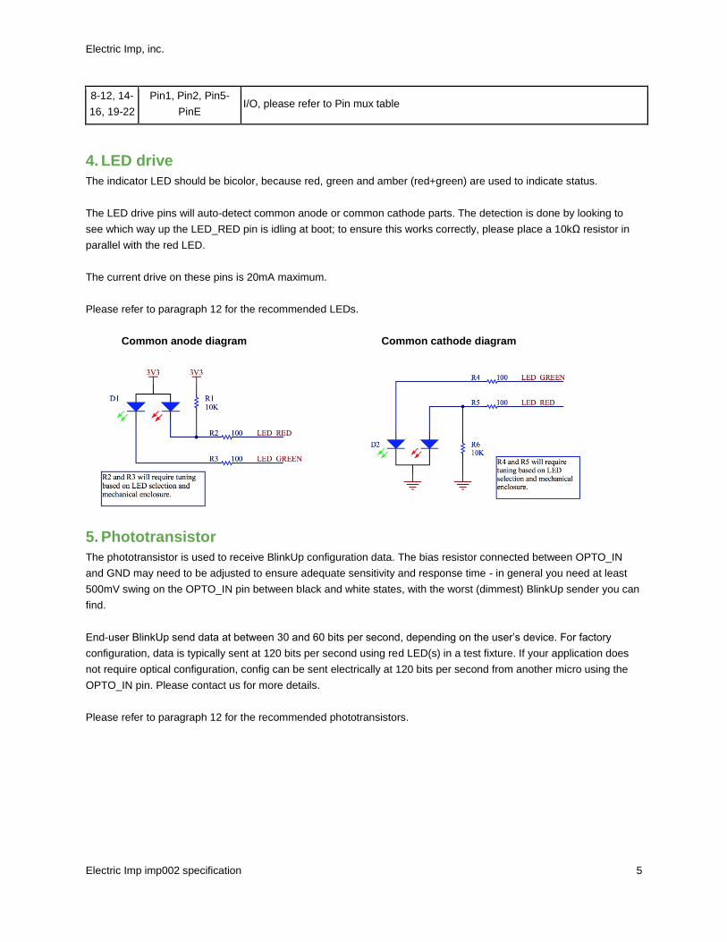
4. LED drive
The indicator LED should be bicolor, because red, green and amber (red+green) are used to indicate status.
The LED drive pins will auto-detect common anode or common cathode parts. The detection is done by looking to
see which way up the LED_RED pin is idling at boot; to ensure this works correctly, please place a 10kΩ resistor in
parallel with the red LED.
The current drive on these pins is 20mA maximum.
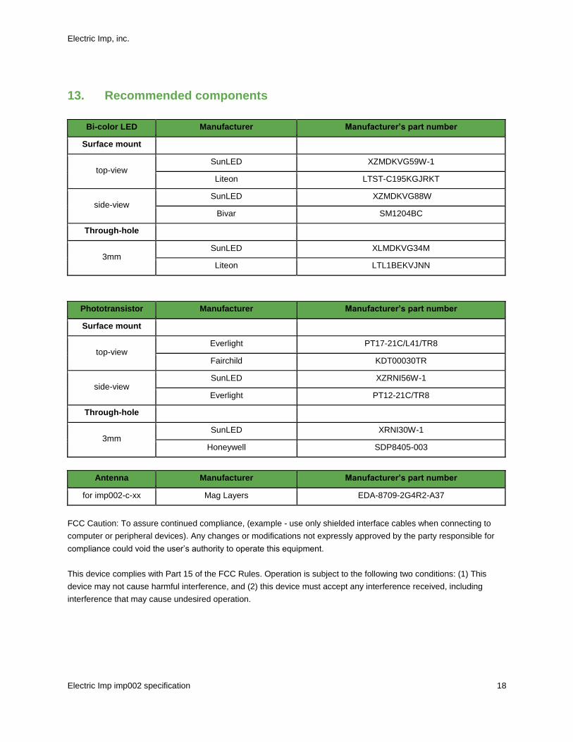
Please refer to paragraph 12 for the recommended LEDs.
Common anode diagram Common cathode diagram
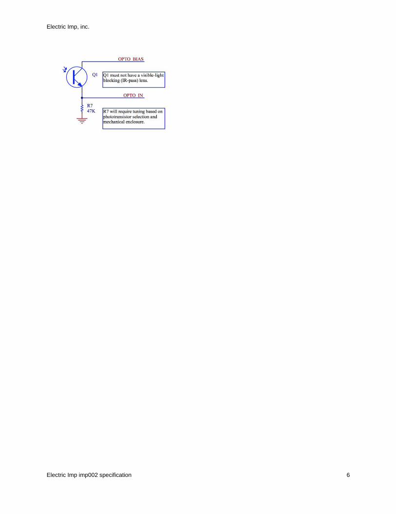
5. Phototransistor
The phototransistor is used to receive BlinkUp configuration data. The bias resistor connected between OPTO_IN
and GND may need to be adjusted to ensure adequate sensitivity and response time - in general you need at least
500mV swing on the OPTO_IN pin between black and white states, with the worst (dimmest) BlinkUp sender you can
find.
End-user BlinkUp send data at between 30 and 60 bits per second, depending on the user’s device. For factory
configuration, data is typically sent at 120 bits per second using red LED(s) in a test fixture. If your application does
not require optical configuration, config can be sent electrically at 120 bits per second from another micro using the
OPTO_IN pin. Please contact us for more details.
Please refer to paragraph 12 for the recommended phototransistors.
Electric Imp, inc.
Electric Imp imp002 specification 6
Electric Imp, inc.
Electric Imp imp002 specification 7
6. External antenna
The imp002-c is the version of imp002 that uses an external antenna. Please refer to paragraph 12 for the
recommended antenna, which is used in our FCC approval.
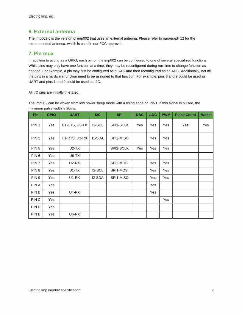
7. Pin mux
In addition to acting as a GPIO, each pin on the imp002 can be configured to one of several specialized functions.
While pins may only have one function at a time, they may be reconfigured during run-time to change function as
needed. For example, a pin may first be configured as a DAC and then reconfigured as an ADC. Additionally, not all
the pins in a hardware function need to be assigned to that function. For example, pins 8 and 9 could be used as
UART and pins 1 and 2 could be used as I2C.
All I/O pins are initially tri-stated.
The imp002 can be woken from low power sleep mode with a rising edge on PIN1. If this signal is pulsed, the
minimum pulse width is 20ms.
Pin GPIO UART I2C SPI DAC ADC PWM Pulse Count Wake
PIN 1 Yes U1-CTS, U3-TX I1-SCL SPI1-SCLK Yes Yes Yes Yes Yes
PIN 2 Yes U1-RTS, U3-RX I1-SDA SPI2-MISO Yes Yes
PIN 5 Yes U2-TX SPI2-SCLK Yes Yes Yes
PIN 6 Yes U6-TX
PIN 7 Yes U2-RX SPI2-MOSI Yes Yes
PIN 8 Yes U1-TX I2-SCL SPI1-MOSI Yes Yes
PIN 9 Yes U1-RX I2-SDA SPI1-MISO Yes Yes
PIN A Yes Yes
PIN B Yes U4-RX Yes
PIN C Yes Yes
PIN D Yes
PIN E Yes U6-RX

Electric Imp, inc.
Electric Imp imp002 specification 8
8. Electrical characteristics
Parameter Description Min Typ Max Unit.
Operating temperature -20 55
VDD Operating voltage 1.8[1]
3.3 3.6 V
VDDA Analog power input 1.8 VDD VDD V
IDD
Normal operation, WiFi on 80 250[2]
mA
Normal operation, WiFi power-save
mode enabled 5 250
[2] mA
WiFi is off, processor sleep, RTC on,
nvram preserved 6 µA
IDDA Current input on VDDA 70 500 µA
VIH I/O input high level voltage 0.7VDD 3.6 V
VIL I/O input low level voltage VSS-0.3 0.3VDD V
IOUT
Output current on any single I/O pin -8 8 mA
Output current on LED_RED pin -20 20 mA
Output current on LED_GREEN pin -20 20 mA
Total output current on all I/O pins
including LED_RED & LED_GREEN -80 80 mA
I/O input leakage current VSS ≦ VIN ≦ VDD 4 µA
Load capacitance Pins 1 to 9 20 pF
Pins A to E 5 pF
[1] WiFi requires 2.5v minimum for operation, but user code can run at 1.8v. The POWER_EN pin is driven to enable
an external boost converter that will provide 2.5v+ during WiFi usage.
[2] 250mA current is during worst-case TX events. These are a maximum of ~4.8ms long (802.11b 1Mbps)
Electric Imp, inc.
Electric Imp imp002 specification 9
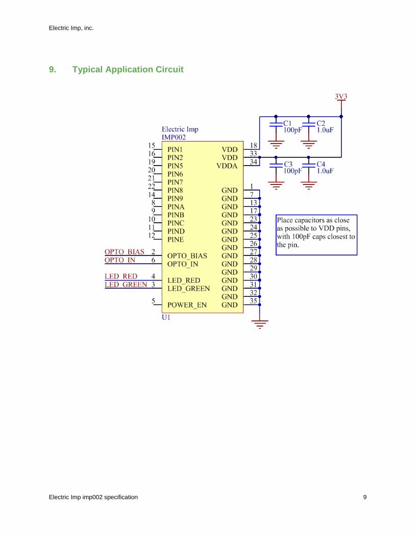
9. Typical Application Circuit

Electric Imp, inc.
Electric Imp imp002 specification 10
10. Package outline
PCB dimensions
(all dimensions are in mm unless otherwise specified)
Electric Imp, inc.
Electric Imp imp002 specification 11
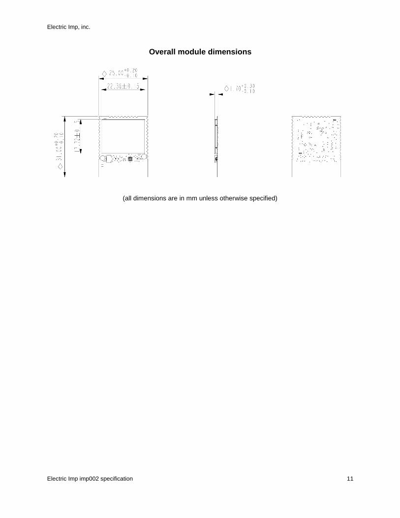
Overall module dimensions
(all dimensions are in mm unless otherwise specified)

Electric Imp, inc.
Electric Imp imp002 specification 12
Tape & reel dimensions

Electric Imp, inc.
Electric Imp imp002 specification 13
Reel disk dimensions
Electric Imp, inc.
Electric Imp imp002 specification 14
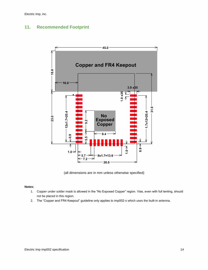
11. Recommended Footprint
(all dimensions are in mm unless otherwise specified)
Notes:
1. Copper under solder mask is allowed in the “No Exposed Copper” region. Vias, even with full tenting, should
not be placed in this region.
2. The “Copper and FR4 Keepout” guideline only applies to imp002-s which uses the built-in antenna.
Electric Imp, inc.
Electric Imp imp002 specification 15
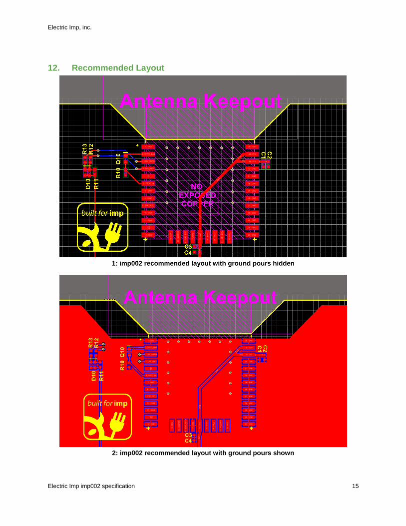
12. Recommended Layout
1: imp002 recommended layout with ground pours hidden
2: imp002 recommended layout with ground pours shown

Electric Imp, inc.
Electric Imp imp002 specification 16
3: imp002 recommended layout shown in 3D
4: imp002 recommended layout shown in 3D, bottom of board

Electric Imp, inc.
Electric Imp imp002 specification 17
Notes:
1. Do not place copper or board material in the antenna keepout area. 2. Ground planes must be poured on the top and bottom layer across the imp footprint, and stitched together
with a row of vias between pin 1 and pin 35 on the imp002. 3. Bypass and filter capacitors should be placed as close as possible to the VDD and VDDA pins.
Electric Imp, inc.
Electric Imp imp002 specification 18
13. Recommended components
Bi-color LED Manufacturer Manufacturer’s part number
Surface mount
top-view SunLED XZMDKVG59W-1
Liteon LTST-C195KGJRKT
side-view SunLED XZMDKVG88W
Bivar SM1204BC
Through-hole
3mm SunLED XLMDKVG34M
Liteon LTL1BEKVJNN
Phototransistor Manufacturer Manufacturer’s part number
Surface mount
top-view Everlight PT17-21C/L41/TR8
Fairchild KDT00030TR
side-view SunLED XZRNI56W-1
Everlight PT12-21C/TR8
Through-hole
3mm SunLED XRNI30W-1
Honeywell SDP8405-003
Antenna Manufacturer Manufacturer’s part number
for imp002-c-xx Mag Layers EDA-8709-2G4R2-A37
FCC Caution: To assure continued compliance, (example - use only shielded interface cables when connecting to
computer or peripheral devices). Any changes or modifications not expressly approved by the party responsible for
compliance could void the user’s authority to operate this equipment.
This device complies with Part 15 of the FCC Rules. Operation is subject to the following two conditions: (1) This
device may not cause harmful interference, and (2) this device must accept any interference received, including
interference that may cause undesired operation.

Electric Imp, inc.
Electric Imp imp002 specification 19
14. Reflow Solder Profile
Pre-heating 120s Max
240° to 250° 3s Max
220°
Reflow 60s Max
150° (Min)
180° (Max)
Degre
es C
Electric Imp, inc.
Electric Imp imp002 specification 20
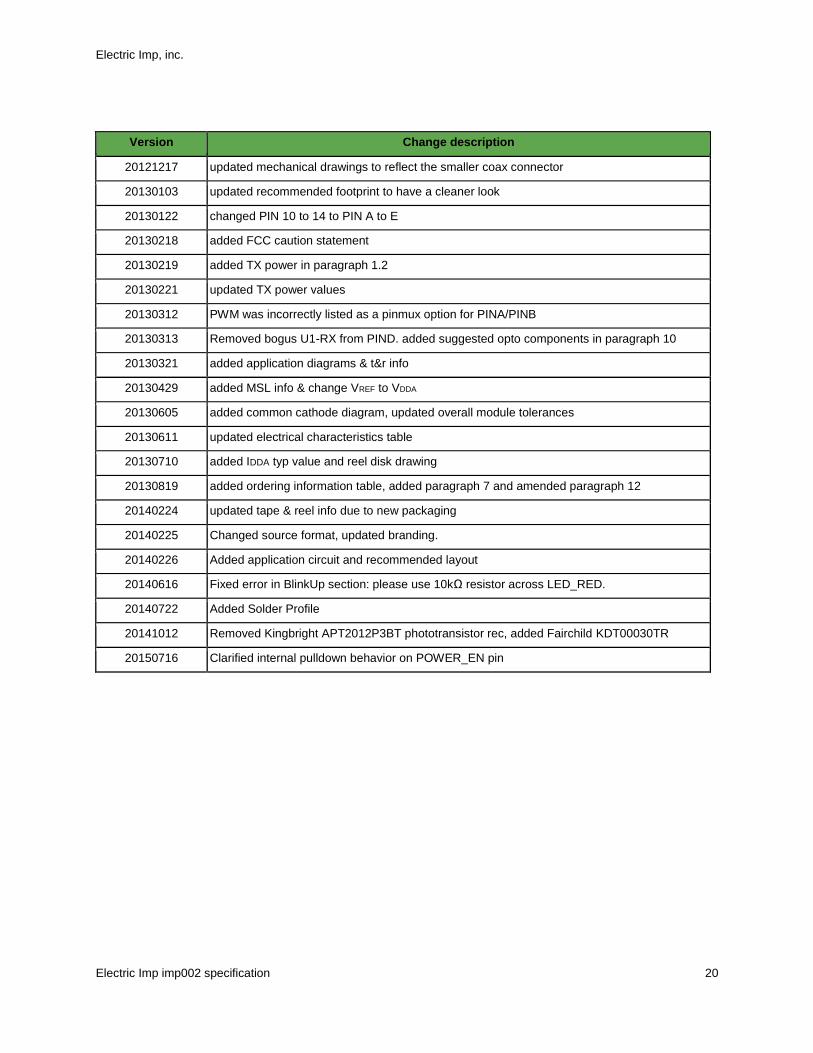
Version Change description
20121217 updated mechanical drawings to reflect the smaller coax connector
20130103 updated recommended footprint to have a cleaner look
20130122 changed PIN 10 to 14 to PIN A to E
20130218 added FCC caution statement
20130219 added TX power in paragraph 1.2
20130221 updated TX power values
20130312 PWM was incorrectly listed as a pinmux option for PINA/PINB
20130313 Removed bogus U1-RX from PIND. added suggested opto components in paragraph 10
20130321 added application diagrams & t&r info
20130429 added MSL info & change VREF to VDDA
20130605 added common cathode diagram, updated overall module tolerances
20130611 updated electrical characteristics table
20130710 added IDDA typ value and reel disk drawing
20130819 added ordering information table, added paragraph 7 and amended paragraph 12
20140224 updated tape & reel info due to new packaging
20140225 Changed source format, updated branding.
20140226 Added application circuit and recommended layout
20140616 Fixed error in BlinkUp section: please use 10kΩ resistor across LED_RED.
20140722 Added Solder Profile
20141012 Removed Kingbright APT2012P3BT phototransistor rec, added Fairchild KDT00030TR
20150716 Clarified internal pulldown behavior on POWER_EN pin


