Soft x-ray nanoanalytical tools for thin film organic electronics
Rainer H. Fink
Friedrich-Alexander University Erlangen-NürnbergPhysical Chemistry 2 (surface & interface science)
http://www.raifi.de
莱纳 · 芬克教授 博士

Chemistry @ FAU: Excellence in research
• Funding: 2013: More than 8.6 million € p.a. third-party funds
2010 – 2012: On average 7.3 € p.a. third-party funds
• DFG Funding Atlas 2012: Number 2 in Germany in DFG based funding
• Taiwan Ranking 2014: World rank: 70
(since 2009: >1,350 papers, 142 JACS or Angew.Ch. and 16 Science or Nature)
• Shanghai Academic Ranking of World Universities 2014: TOP 75, #1 in FAU
FAU relationship to ACES / UoW
• International student exchange programs (since 2006)
• Double degree programs: M.Sc. „Chemistry – in International Degree“
• Joint PhD program
• D. Guldi – Co-PI at ACES (dye-sensitized solar cells)

Synthetic Carbon AllotropesOrganic Nanostructures, molecular wires
Supramolecular Chemistry
Time-resolved charge transfer
Photovoltaics / artificial leaves / energy
From molecules to materials & devices
Our department focuses on ...
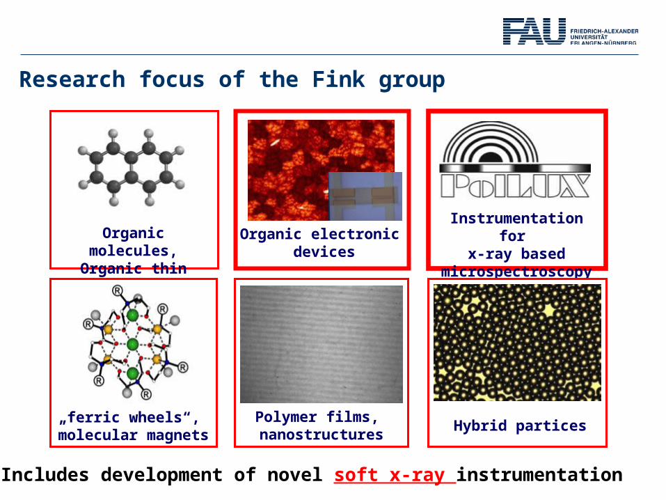
Research focus of the Fink group
Organic molecules,Organic thin films
Polymer films, nanostructures
Organic electronic devices
Instrumentation for x-ray based
microspectroscopy
„ferric wheels“, molecular magnets
Hybrid partices
Includes development of novel soft x-ray instrumentation
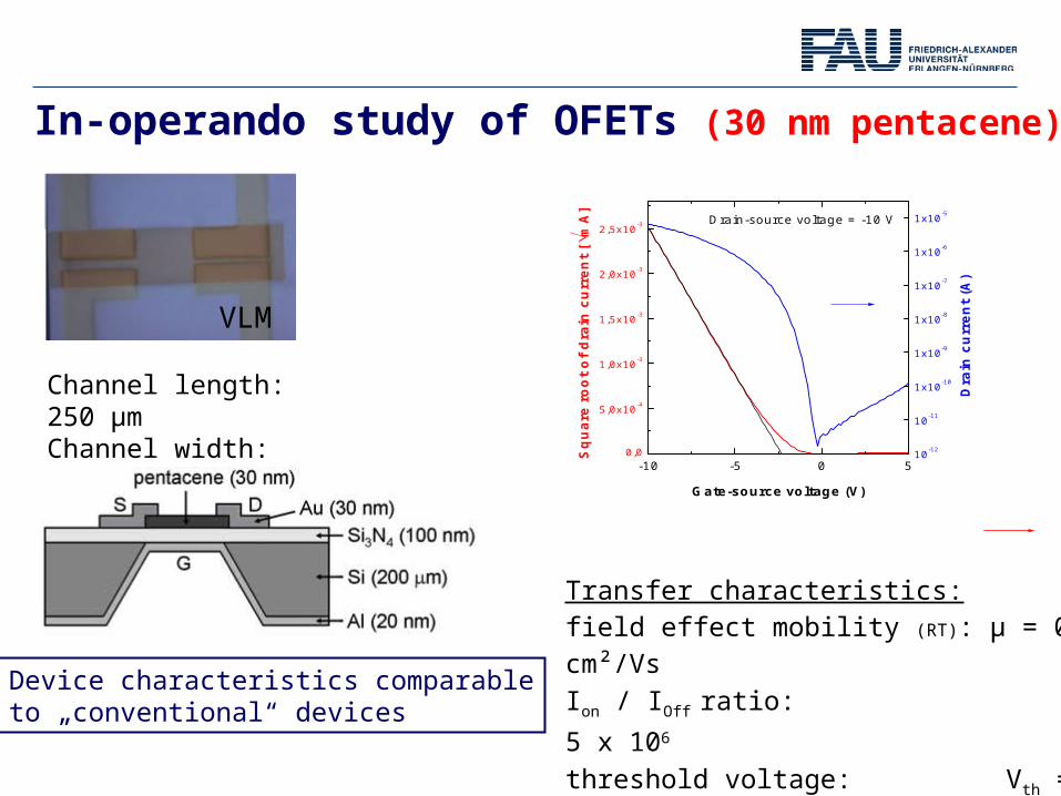
In-operando study of OFETs (30 nm pentacene)
Channel length: 250 μmChannel width: 20/40 μm
Device characteristics comparableto „conventional“ devices
-10 -5 0 50,0
5,0x10⁻⁴
1,0x10⁻³
1,5x10⁻³
2,0x10⁻³
2,5x10⁻³ Drain-source voltage = -10 V
Gate-source voltage (V)
Sq
uare
ro
ot
of
dra
in c
urr
en
t [
mA
]
10-12
10-11
1x10⁻¹⁰
1x10⁻⁹
1x10⁻⁸
1x10⁻⁷
1x10⁻⁶
1x10⁻⁵
Dra
in c
urr
en
t (A
)
Transfer characteristics:field effect mobility (RT): μ = 0.6 cm²/Vs
Ion / IOff ratio: 5 x 10⁶
threshold voltage: Vth = -2.3 V
subthreshold slope: S ≈ 0.3 V/dec
VLM
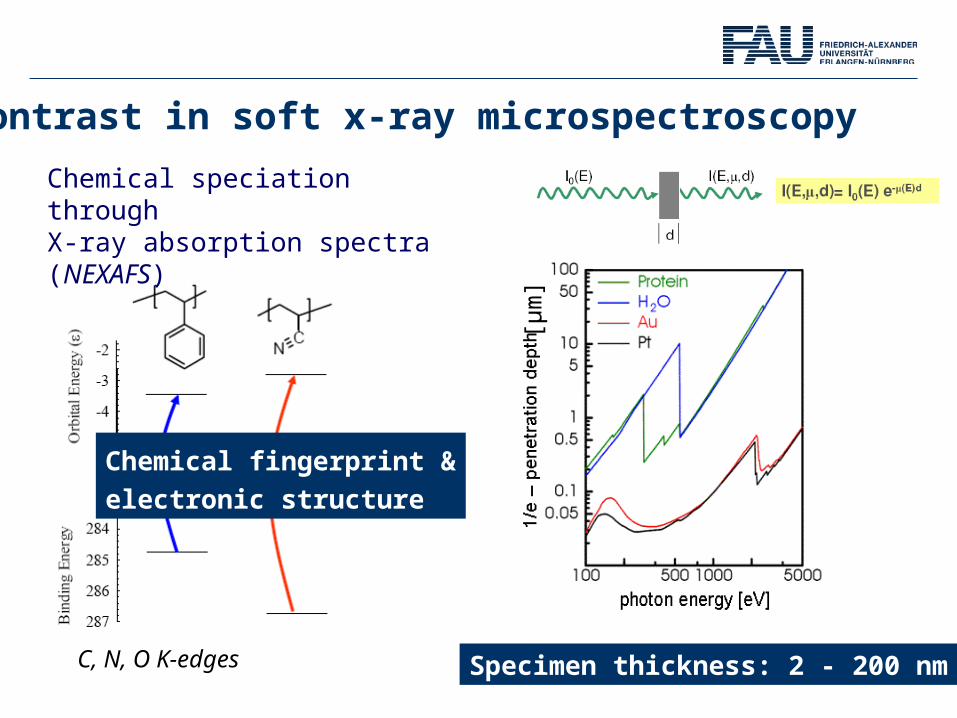
Contrast in soft x-ray microspectroscopy
Chemical speciation through X-ray absorption spectra (NEXAFS)
C, N, O K-edges
[µm
]
Specimen thickness: 2 - 200 nm
Chemical fingerprint &
electronic structure
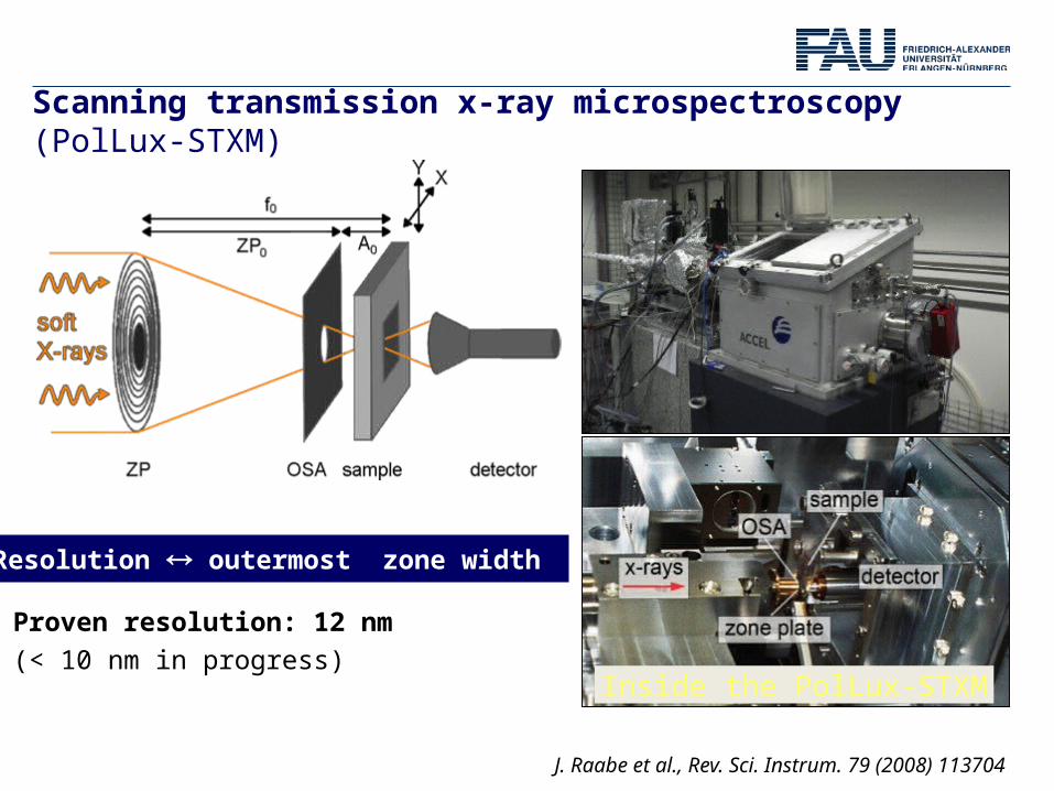
Scanning transmission x-ray microspectroscopy (PolLux-STXM)
J. Raabe et al., Rev. Sci. Instrum. 79 (2008) 113704
Inside the PolLux-STXM
Resolution outermost zone width
Proven resolution: 12 nm
(< 10 nm in progress)

Film morphology/molecular orientation - DHDAP
STXM FOV 20 x 20 mm2
AFM 5 x 5 mm2
On Si3N4On Al/Al2O3
reso
nan
t3
10 e
V

STXM / NEXAFS
1 µm
X-ray polarization
C 1s π* resonance at 283.3 eV
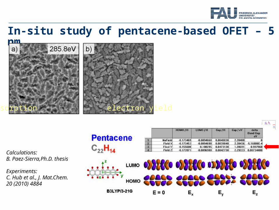
In-situ study of pentacene-based OFET – 5 nm
Calculations: B. Paez-Sierra,Ph.D. thesis
Experiments:C. Hub et al., J. Mat.Chem. 20 (2010) 4884
282 284 286 288 290
UG: 0V / U
D: 0V
inte
nsity [a.u
.]
UG: -10V / U
D: -10V
absorption electron yield
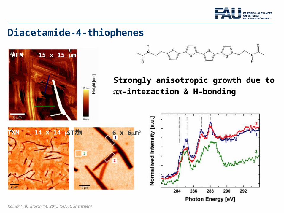
Diacetamide-4-thiophenes
AFM 15 x 15 mm2
STXM 14 x 14 mm2 STXM 6 x 6mm2
Strongly anisotropic growth due to
pp-interaction & H-bonding
Rainer Fink, March 14, 2015 (SUSTC Shenzhen)

OFET studies
3 nm Ac4T (p-type)
within active channel
hv = 287,5 eV
12 x 12 µm2
gate effect: yestransport effect: no !
Number of charge carriers is too low
(injection limited !)
Charge trapping ?
SAMFETs
All functionalities in one molecule
M. Halik and A. Hirsch, Adv. Mater. 23 (2011) 2689
(ongoing STXM study)
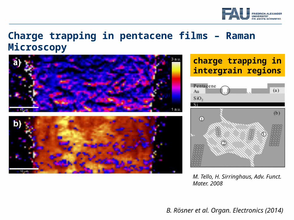
Charge trapping in pentacene films – Raman Microscopy
B. Rösner et al. Organ. Electronics (2014)
M. Tello, H. Sirringhaus, Adv. Funct. Mater. 2008
charge trapping in intergrain regions

reaction in solution reaction in the gas phase
5 µm
SEM
1 µm
SEM
1 µm
SEM
clo
sed
silv
er f
ilm
clo
sed
silv
er f
ilm
80° sample tilt
Ag (30 nm)
Si substrate
p = 10-2 mbarT = 90°-150°CAg (30 nm)
saturated TCNQ solution
Si substrate
in acetonitrile saturated TCNQ vapour phase
Ag-TCNQ CT-complexes
Electronically bistable Electrocatalytically activePhotoactivity
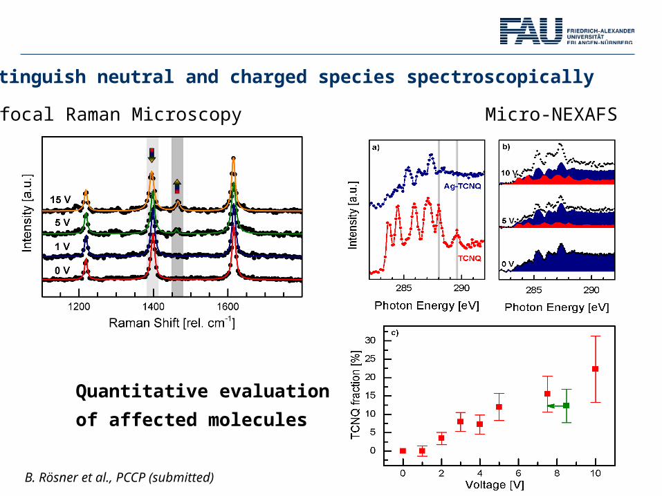
Distinguish neutral and charged species spectroscopically
Confocal Raman Microscopy Micro-NEXAFS
Quantitative evaluation
of affected molecules
B. Rösner et al., PCCP (submitted)
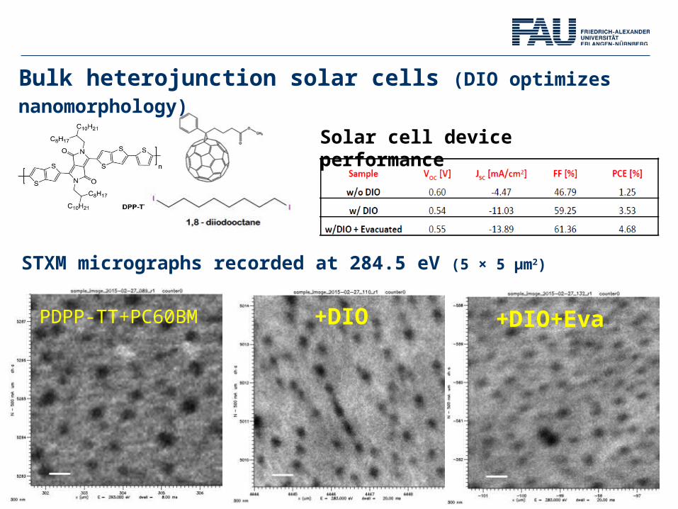
Solar cell device performance
PC60BM +DIO +DIO+Eva
STXM micrographs recorded at 284.5 eV (5 × 5 µm2)
PDPP-TT+PC60BM
Bulk heterojunction solar cells (DIO optimizes nanomorphology)
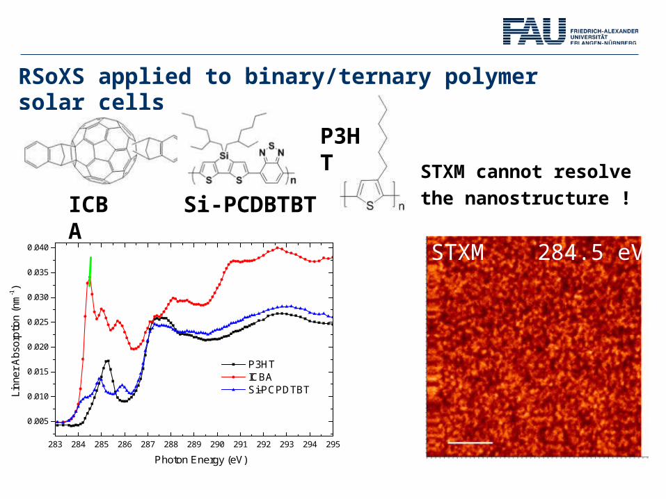
RSoXS applied to binary/ternary polymer solar cells
ICBA Si-PCDBTBT
283 284 285 286 287 288 289 290 291 292 293 294 295
0.005
0.010
0.015
0.020
0.025
0.030
0.035
0.040
P3HT ICBA Si-PCPDTBT
Lin
ner
Abso
rptio
n (
nm
-1)
Photon Energy (eV)
P3HT
STXM 284.5 eV
STXM cannot resolve
the nanostructure !
10-8
10-7
10-6
Co
ntra
st (
)
290285280275270
Energy [eV]
Orientation Density
Contrast Functions
Inte
nsity
[au]
4 5 60.01
2 3 4 5 60.1
2 3 4
q [nm-1
]
1000 100 202/q [nm]
270 eV
P-SoXS Profiles
Inte
nsity
[au]
4 5 60.01
2 3 4 5 60.1
2 3 4
q [nm-1
]
1000 100 202/q [nm]
270 eV 284.2 285.9 289
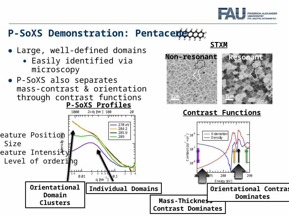
● Large, well-defined domains● Easily identified via microscopy
● P-SoXS also separates mass-contrast & orientation through contrast functions
2μm2μm
Non-resonant Resonant
STXM
Mass-Thickness Contrast Dominates
Orientational ContrastDominates
Individual DomainsOrientational Domain Clusters
Feature Position = Size
Feature Intensity = Level of ordering
P-SoXS Demonstration: Pentacene
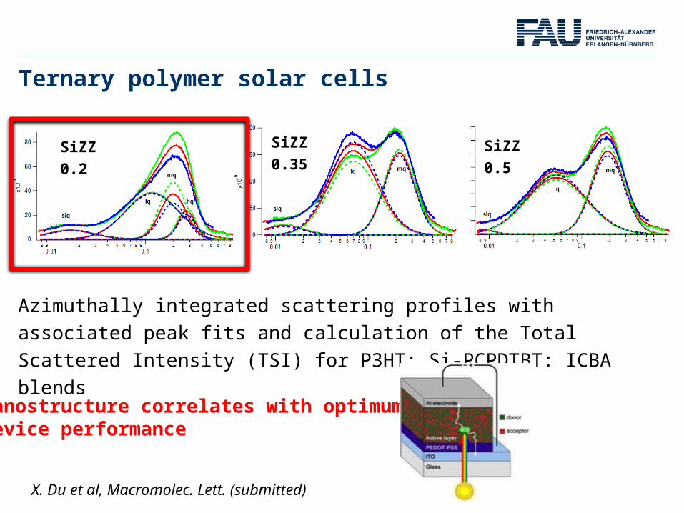
Ternary polymer solar cells
X. Du et al, Macromolec. Lett. (submitted)
Azimuthally integrated scattering profiles with associated peak fits and
calculation of the Total Scattered Intensity (TSI) for P3HT: Si-PCPDTBT: ICBA
blends
SiZZ
0.2
SiZZ
0.35 SiZZ
0.5
Nanostructure correlates with optimum device performance

Summary & conclusions
●STXMs offer superb resolution based on recent zone plate developments
●NEXAFS detects modifications in the unoccupied DOS in OFETs under operation – still some issues with potential energy shifts (p-materials ?)
●Combine STXM with complementary microscopies to access interesting material properties (especially in-situ microspectroscopy)
●RSoXS complements STXM for structures below the ZP resolution limit
●NanoXAS: combine STXM and AFM at same spot
x-rays
z
Cantilever


