
SoC TAM Design to Minimize Test Application Time
Huiting ZhangVishwani D. Agrawal
May 12, 2015
2015 North Atlantic Test Workshop

Motivation
With rapid growth of system-on-chip (SoC) size,
there has been an enormous increase in test
application time (TAT).
Current SoC test scheduling fails to incorporate
various hardware and power constraints
introduced in this paper.
May 12, 2015 1
Proposed Work
The first part is test access mechanism (TAM) design
- Make effective use of SoC testing resources.
- Minimize wiring complexity of previous fork and merge method.
The second part is test scheduling
- Include various hardware constraints in SoC test scheduling.
- Dynamic voltage and frequency scaling is adopted to reduce TAT.
May 12, 2015 2

3
Components of SoC test:Source – to apply test stimuliSink – to capture test resultsTAM – to transport test patterns and test responseWrapper – Interface between TAM and cores
Testing of SoC
May 12, 2015

Fixed-Width TAM Architecture
Disadvantage: TAM assignment cannot be explicitly tailored to
each core’s needs.
Advantage: The wiring of TAM buses is simpler.
4May 12, 2015
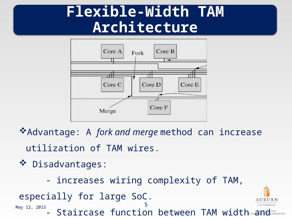
Flexible-Width TAM Architecture
Advantage: A fork and merge method can increase utilization of
TAM wires.
Disadvantages:
- increases wiring complexity of TAM, especially for large SoC.
- Staircase function between TAM width and test time.May 12, 2015 5
Proposed TAM Design
Allows flexibility on internal scan chain redesign and layout
arrangement of cores.
Optimal core arrangement allows easy wiring of TAM.
Test time drops linearly with increasing TAM through internal
scan chain redesign.
May 12, 2015 6
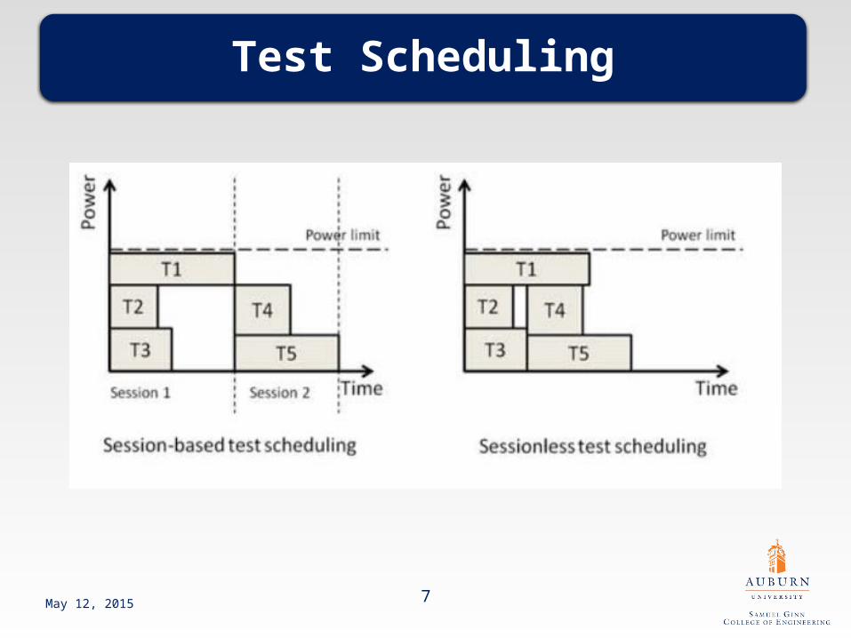
Test Scheduling
7May 12, 2015
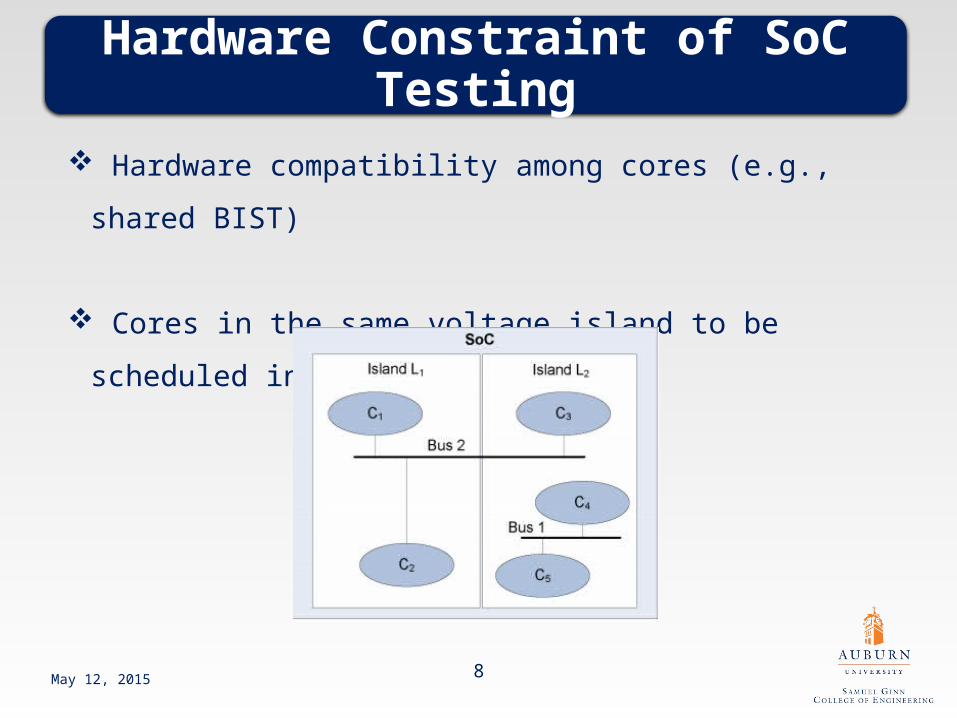
Hardware Constraint of SoC Testing
Hardware compatibility among cores (e.g., shared BIST)
Cores in the same voltage island to be scheduled in parallel
8May 12, 2015

9
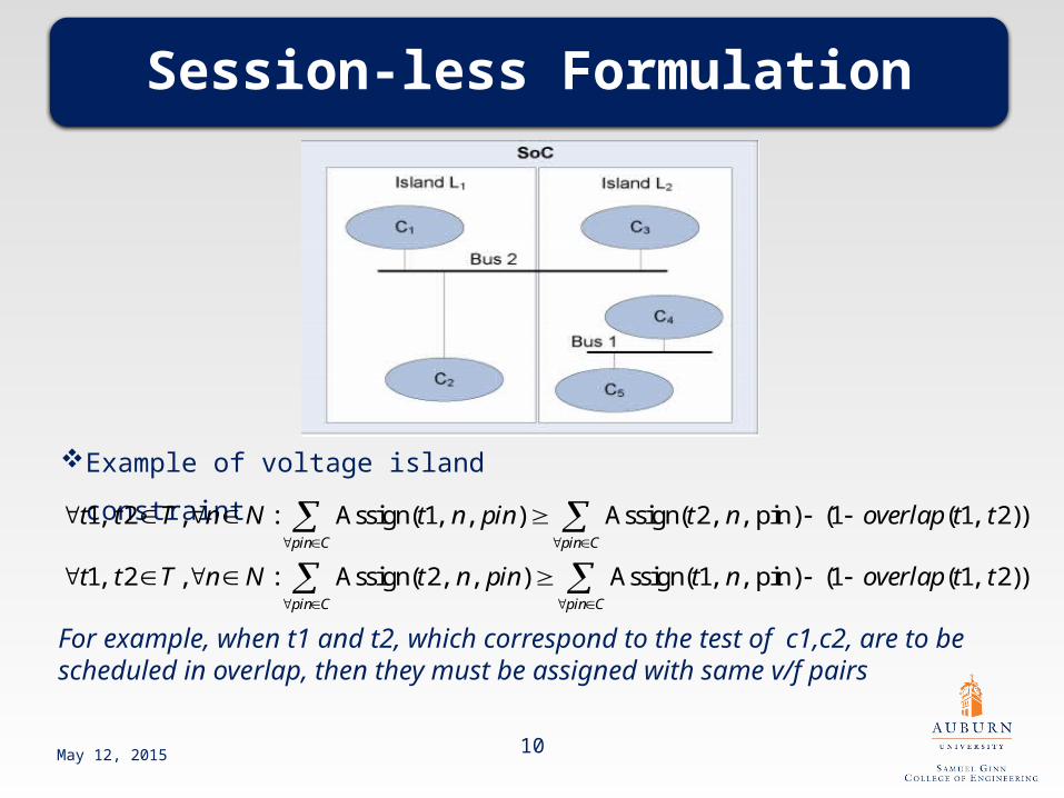
Session-less Formulation
This formulation is only partly shown.
Need formulation for hardware and power constraints, and TAM bounds
:
:
: 0
1, / ,
, , .
0, .
( )
( )
: , , 1
( ) ( )
( )
( )
( )pin C
t T tfinish F t
t T F t S t L t
t T S t
if test t are executed with nth v f pairs
Assign t n pin and assigned with TAM pin choice
Otherwise
t T Assign t n pin
: , ,( )* , ,( )
n N
n N pin C
t T L t Assign t n pin Lt n pin
May 12, 2015
MILP Objective is to minimize TAT
Lt,n,pin is the test time of t with nth v/f pair and assigned TAM choice
Session-less Formulation
10May 12, 2015
Example of voltage island constraint
1, 2 , : 1, , 2, , pin 1 1, 2
1, 2 , : 2, , 1, , pi
Assign( ) Assign( ) ( ( ))
Assign( ) Assign( ) ( ( ))n 1 1, 2
pin C pin C
pin C pin C
t t T n N t n pin t n overlap t t
t t T n N t n pin t n overlap t t
For example, when t1 and t2, which correspond to the test of c1,c2, are to be scheduled in overlap, then they must be assigned with same v/f pairs
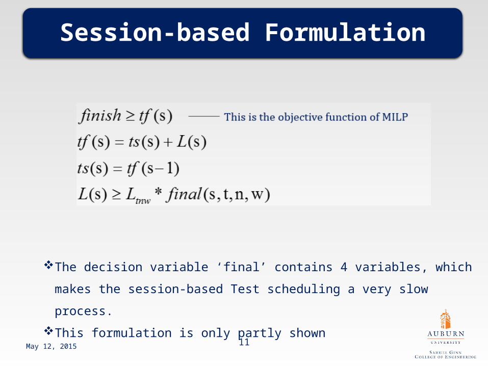
Session-based Formulation
11
The decision variable ‘final’ contains 4 variables, which makes the session-based
Test scheduling a very slow process.
This formulation is only partly shown
May 12, 2015

Experimental Setup
12
May 12, 2015
The benchmark used in this work is from ITC’02 benchmark
set

13
Result 1: No DVFS, No TAM Design
Up to 69% of reduction in TAT is achieved with TAM
design and DVFS
May 12, 2015
14
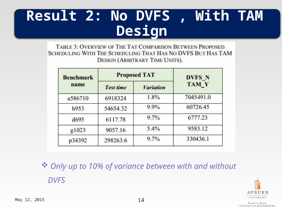
Result 2: No DVFS , With TAM Design
May 12, 2015
Only up to 10% of variance between with and without
DVFS

15
Result 3: With DVFS, No TAM Design
May 12, 2015
Up to 61% of variance between with and without TAM
Design, which signify the effectiveness of TAM Design in
TAT reduction

Result 4: TAT Saving by TAM Design
Reference work doesn’t consider hardware compatibility,
Voltage Island and TAM bounds!
16May 12, 2015
17
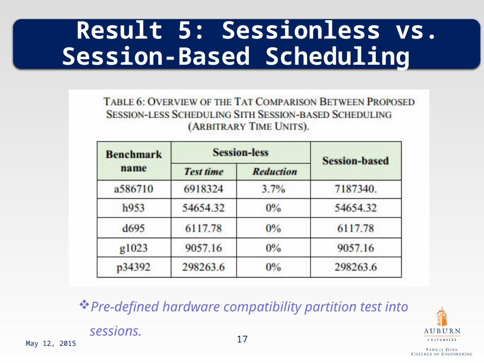
Result 5: Sessionless vs. Session-Based Scheduling
May 12, 2015
Pre-defined hardware compatibility partition test into
sessions.
Conclusion
The proposed TAM design leads to noticeable improvement in the
test scheduling. The novel idea of this paper is to allow flexibility in
scan chain organization and core arrangement by incorporating
TAM design as part of the SoC design process. In this way, SoC
resources are effectively used and the TAT is reduced.
This is an attempt at complete modeling of SoC testing under
hardware and power constraints, which have not been addressed
together all at once in the previous work.
18May 12, 2015
In this work, SoC hierarchy is not considered. In real SoC, TAM
allocation between parent cell and children cells are more difficult.
ITC’02, the most adopted SoC benchmarks so far are incomplete. For
accurate test scheduling result, more details are needed.
Some faults are only detectable at certain voltage.
The flexibility of modification on core arrangement and scan chain
redesign may not be allowed for some cores in SoC.
Limitation
May 12, 2015 19

References1. S. Millican and K. K. Saluja, “Optimal Test Scheduling of Stacked Circuits under Various
Hardware and Power Constraints,” Proc. 28th International Conference on VLSI Design, pp. 487-492, Jan. 2015.
2. 3DIC SoC Test Benchmarks, url:http://3dsocbench.ece.wisc.edu/
3. V. Iyengar, K. Chakrabarty, and E. J. Marinissen, “Test Access Mechanism Optimization, Test Scheduling, and Tester Data Volume Reduction for System-on-Chip,” IEEE Transactions on Computers, vol. 52, no. 12, pp. 1619-1631, Dec. 2003.
4. ITC2002 SOC Benchmarking Initiative. Duke University. http://www.extra.research.philips.com/itc02socbenchm
5. V. Sheshadri, V. D. Agrawal, and P. Agrawal, “Power Aware SoC Test Optimization Through Dynamic Voltage and Frequency Scaling,” Proc. 21st International Conference on VLSI-SoC, pp. 102- 107, Oct. 2013.
6. V. Sheshadri, V. D. Agrawal, and P. Agrawal, “Optimum Test Schedule for SoC with Specified Clock Frequencies and Supply Voltages,” Proc. 26th International Conference on VLSI Design and International Conference on Embedded Systems, pp. 267-272 , Jan. 2013.
7. C. R. Kime and K. K. Saluja, “Test Schduling in Testable VLSI Circuits,” Proc. 25th IEEE International Symposium on Fault Tolerant Computing, Santa Monica, pp. 406-412, 1982.
21May 12, 2015

22
References8. K. Chakrabarty, “Test Scheduling for Core-Based Systems Using Mixed-Integer Linear
Programming,” IEEE Trans ComputerAided Des of Integr Circ. and Syst., vol. 19, no. 10, pp. 1163-1174, Oct. 2000.
9. R. M. Chou, K. K. Saluja, and V. D. Agrawal, “Scheduling Tests for VLSI Systems Under Power Constraints,” IEEE Trans. VLSI Systems, vol. 5, no. 2, pp. 175-185, June 1997.
10. T. Sakurai, “Alpha Power-Law Model,” IEEE Solid-State Circuits Society Newsletter, vol. 9, no. 4, pp. 4-5, Oct. 2004.
11. S. Millican and K. K. Saluja "Formulating Optimal Test Scheduling Problem with Dynamic Voltage and Frequency Scaling," Proc. 22nd Asian Test Symposium, pp. 165-170, Nov. 2013.
12. E. Larsson and H. Fujiwara, “Power Constrained Preemptive TAM Scheduling” Proc. Seventh IEEE European Test Workshop, pp.119- 126, Nov. 2002.
13. V. Iyengar, K. Chakrabarty, and E. J. Marinissen. “Test Wrapper and Test Access Mechanism Co-Optimization for SoC,” Proc. International Test Conference., pp. 1023-1032, Oct. 2001.
14. D. R. Bild, S. Misra, T. Chantemy, P. Kumar, R. P. Dick, X. S. Hu, L. Shang, and A. Choudhary, “Temperature-Aware Test Scheduling for Multiprocessor Systems-on Chip,” Proc. IEEE/ACM International Conference on Computer-Aided Design, pp. 59 66, Nov. 2008.
May 12, 2015

Questions?
THANK YOU
May 12, 2015


