
1
Silicon Detectors for the Super LHC
Sally Seidel University of New Mexico
for the RD50 Collaboration
Twelfth Vienna Conference on Instrumentation 17 February 2010

2

3
249 scientists and engineers from 47 member institutes:
Barcelona, Bari, BNL, Bucharest NIMP, Uni. Bucharest, CERN, Dortmund, Erfurt, Fermilab, Florence, Freiburg, Glasgow, Hamburg, Helsinki HIP, Ioffe Inst., ITE, ITME, Karlsruhe, KINR, Lancaster, Lappeenranta, Liverpool,
Ljubljana, Louvain, Minsk, Montreal, Moscow ITEP, Munich, New Mexico, Nikhef, Uni. Oslo, Padova, Perugia, Pisa, Prague Academy, Prague Charles, Prague CTU, PSI, Purdue, Rochester, UC Santa Cruz, SINTEF, Syracuse, Tel Aviv, Trento, Valencia, Vilnius

4
Super LHC (sLHC) is a proposed upgrade of the LHC to luminosity 1035cm-2s-1.
Expected hadron fluence at r ~ 4cm: 1.6 x 1016 cm-2 neq.
The primary limitation is trapping: decrease in charge collection efficiency.
Timescale for start of sLHC under discussion, ≥ 2018.

5
Predicted fluences (neq), including safety factor 2:
B layer (r = 3.7 cm) 2.5 x 10¹⁶ (1140 MRad) Inner pixel layer (r = 5 cm): 1.4 x 10¹⁶ (712 MRad) Second pixel layer (r = 7 cm): 7.8 x 10¹⁶ (420 MRad) Outer pixel layer (r = 11 cm): 3.6 x 10¹⁵ (207 Mrad) Short strips (r = 38 cm): 6.8 x 10¹⁴ (30 Mrad) Long strips (r = 85 cm): 3.2 x 10¹⁴ (8.4 Mrad)
Pixels
Radial distribution of sensors determined by occupancy < 2%, still emerging
Short Strips
LongStrips

6
Reported here:
Connections between microscopic defect properties and macroscopic sensor properties Epitaxial silicon Magnetic Czochralski (MCz) silicon sensors p-type silicon sensors 3D silicon sensors New structures
What follows is just a sample of recent results. For the full story, please see rd50.web.cern.ch/rd50/.

7
Use of High Resolution Photo-induced Transient Spectroscopy to compare radiation defects in standard
and oxygenated epitaxial Si
P. Kamiński, R. Kozłowski, J. Żelazko, M. Kozubal, E. Fretwurst
24 GeV p
Higher [O] mainly affects shallow traps related to interstitial aggregates.
After annealing to 240°C, mid-gap traps develop independent of [O].
# traps is maximized in standard and oxygenated epi layers after annealing at 80 and 160 °C.
A study of trap parameters and concentration versus oxygenation level, annealing parameters, and fluence

8
Use of High Resolution Photo-induced Transient Spectroscopy to compare radiation defects in standard
and oxygenated epitaxial Si, continued
P. Kamiński, R. Kozłowski, J. Żelazko, E. Fretwurst
Example result, for Φ = 1.7 x 10¹⁶ p cm-2:
Conclusions: • Dominant trap in low-fluence standard n-epi is at 410 meV, likely I2O, conc. 5.2 x 1016 cm-3. As fluence rises, 315 meV trap dominates, likely VxOy, conc. 5.8 x 1016 cm-3. • In oxygenated n-epi, 420 meV trap dominates at all fluences, likely V2
-/0. • After 1 hr 240°C anneal, dominant defect at 575 meV.
9
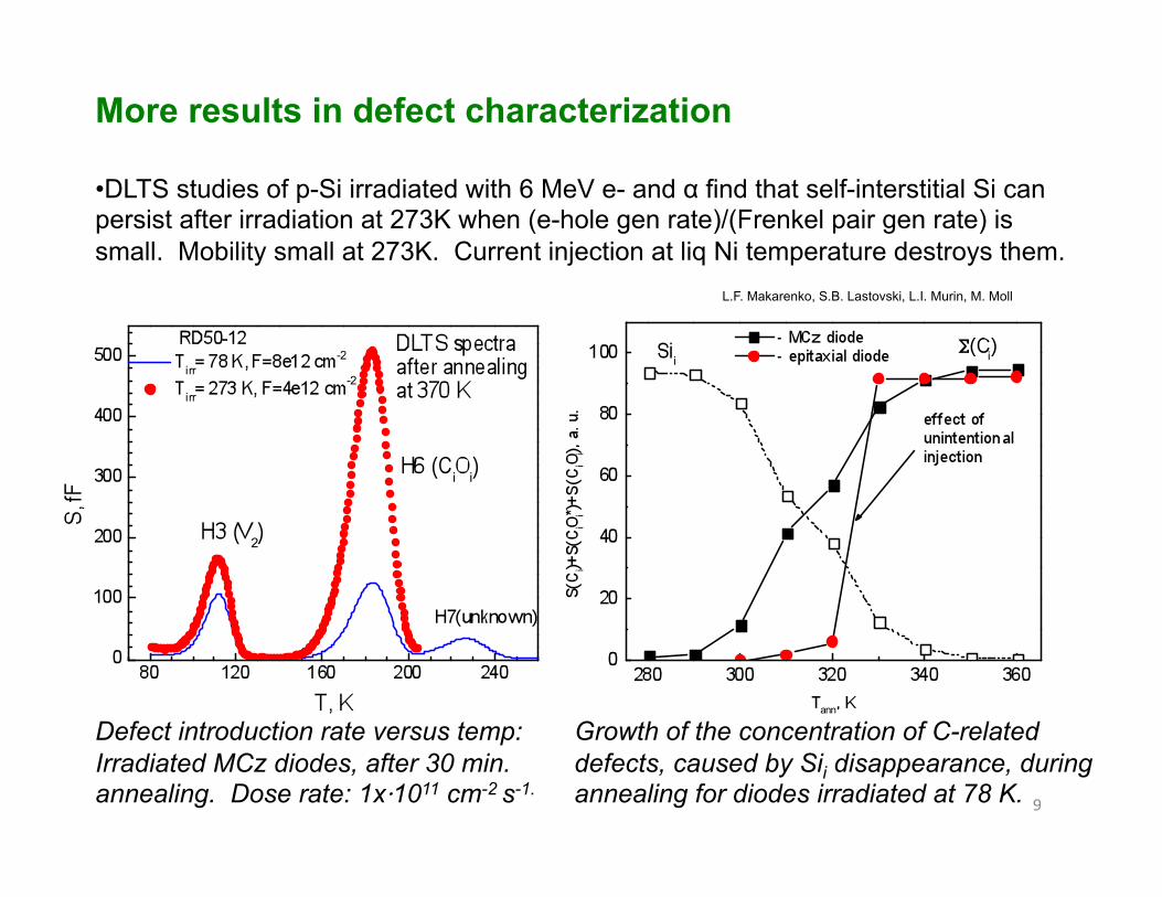
More results in defect characterization
• DLTS studies of p-Si irradiated with 6 MeV e- and α find that self-interstitial Si can persist after irradiation at 273K when (e-hole gen rate)/(Frenkel pair gen rate) is small. Mobility small at 273K. Current injection at liq Ni temperature destroys them.
Growth of the concentration of C-related defects, caused by Sii disappearance, during annealing for diodes irradiated at 78 K.
Defect introduction rate versus temp: Irradiated MCz diodes, after 30 min. annealing. Dose rate: 1x⋅1011 cm-2 s-1.
L.F. Makarenko, S.B. Lastovski, L.I. Murin, M. Moll

10
Defect characterization:
Shallow donor E(30K) generated by electron irradiation of n-type FZ diodes. E(30K), a cluster defect associated with non-type inversion of epi diodes after high p fluence, overcompensates deep acceptors. E(30K) generation is suppressed for high electron energies---suggesting point-like character?
A. Junkes, E. Fretwurst, I. Pintilie, G. Lindström

11
Defect characterization:
TSC study of p- and n-type MCz Si irradiated with reactor n up to 1016 cm-2. Features correspond qualitatively to band diagrams. Interpretation: presence of residual electric field (polarization of the irradiated Si bulk) due to frozen charged traps in bulk and barriers close to electrodes. Residual field is opposed to external Vbias.
M. Scaringella, M. Bruzzi, D. Menichelli, R. Mori

12
Epitaxial silicon
Benefits: oxygenation and controlled thin layer growth

13
TCT studies and simulation of charge collection in 150µm-thick epi devices after ϕ=(1 - 4) x 1015 cm-2 reveal field-dependent contribution to lifetimes.
τ = τ0 + τ1 E
T. Pöhlsen, J. Becker, E. Fretwurst, R. Klanner, J. Lange

14
Charge collection, trapping well described by including:
distortions to the space charge distribution leading to parabolic electric fields (double peak)
field-dependence of trapping time τ (to fit CCE curves)
electronic circuit effects (to simulate TCT signals)
Trapping probability decreases with increasing E-field: high E-fields desirable to reduce trapping probability
300 V / 150 µm
900 V / 150 µm
T. Pöhlsen, J. Becker, E. Fretwurst, R. Klanner, J. Lange
Epitaxial Si, continued

15
Studies of charge multiplication in highly irradiated sensors Please see talk by Lange, Junkes, et al. n-type epitaxial, [O] = 9x1016cm-3, <111>, Neff,0=2.6x1013cm-3
Beneficial Charge Multiplication in highly irradiated (1016cm-2 24-GeV p) devices due to impact ionization provides proportional response, long-term stability, homogeneous production, only slight noise increase.
J. Lang, J. Becker, E. Fretwurst, R. Klanner, G. Lindström
16
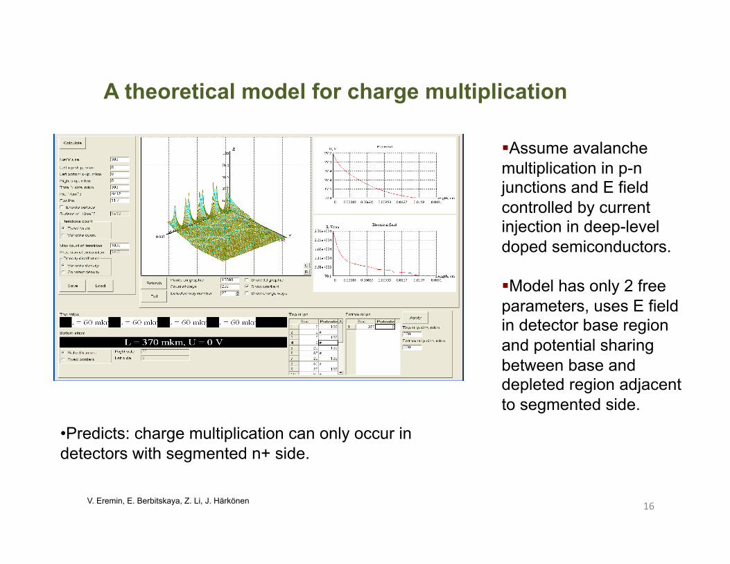
A theoretical model for charge multiplication
V. Eremin, E. Berbitskaya, Z. Li, J. Härkönen
Assume avalanche multiplication in p-n junctions and E field controlled by current injection in deep-level doped semiconductors.
Model has only 2 free parameters, uses E field in detector base region and potential sharing between base and depleted region adjacent to segmented side.
• Predicts: charge multiplication can only occur in detectors with segmented n+ side.

17
Czochralski silicon Please see also the talk by L. Spiegel
Benefit: enhanced oxygenation intrinsic to the process

18
Comparison of Vdep and Ileak in n-Fz and n-MCz after (24 GeV) proton and (300 MeV) pion irradiation
MCz: 1 kΩ-cm (Vdep 300V); FZ: 15 kΩ-cm (Vdep 20V)
Collected charge on MCz > on FZ
Collected charge less after pion than after proton irradiation
Conclusions: trapping probability lower after pion irradiation; hole trapping different for FZ and MCz.
Collected charge @ 300 V
Czochralski studies of charge collection versus fluence
K. Kaska, M. Fahrer, M. Moll
PRELIMINARY

Parameters of the ‘four trap level model’ for n-type MCz Si
Device modeling of neutron damage effects in n-MCz Si
Good agreement in Vfull dep and Ileak between simulation (Synopsys TCAD) and data. Theoretical calculations based on Shockley Read Hall recombination theory reproduce the Vfull dep data but underestimate the measured Ileak at 293K. Plan: mixed irradiation model (n-MCz Si) for charge carrier trapping, electric field distribution.
A. K. Srivastava, D. Eckstein, E. Fretwurst, R. Klanner, G. Steinbrück

20
Low resistivity n-Czochralski:
• Motivated by challenges to strip isolation in p-type.
• Competitive with p-FZ up to few x 1015 n.
• Good CCE up to 10000 min @ 60°C.
• The challenge: high current. N. Pacifico, E. del Castillo Sanchez, M. Fahrer, M. Moll

21
Mixed irradiation of sensors in Czochralski silicon
Irradiated with neutron-proton mix with charged/neutral as expected at sLHC
R. Eber, Th. Müller, W. de Boer, A. Dierlamm, M. Frey, P. Steck, T. Barvich

22
Mixed irradiation of sensors in Czochralski silicon, continued Trapping times extracted for fluences < 1015 cm-2 neq
Defect sources....gold?
R. Eber, Th. Müller, W. de Boer, A. Dierlamm, M. Frey, P. Steck, T. Barvich
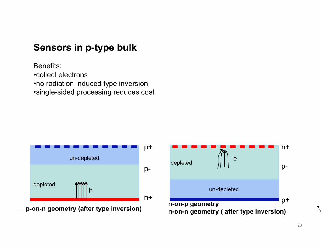
un-depleted
un-depleted depleted
depleted e
h
p+
p-
p+
p-
n+
n+
p-on-n geometry (after type inversion) n-on-p geometry n-on-n geometry ( after type inversion)
23
Sensors in p-type bulk
Benefits: • collect electrons • no radiation-induced type inversion • single-sided processing reduces cost
24
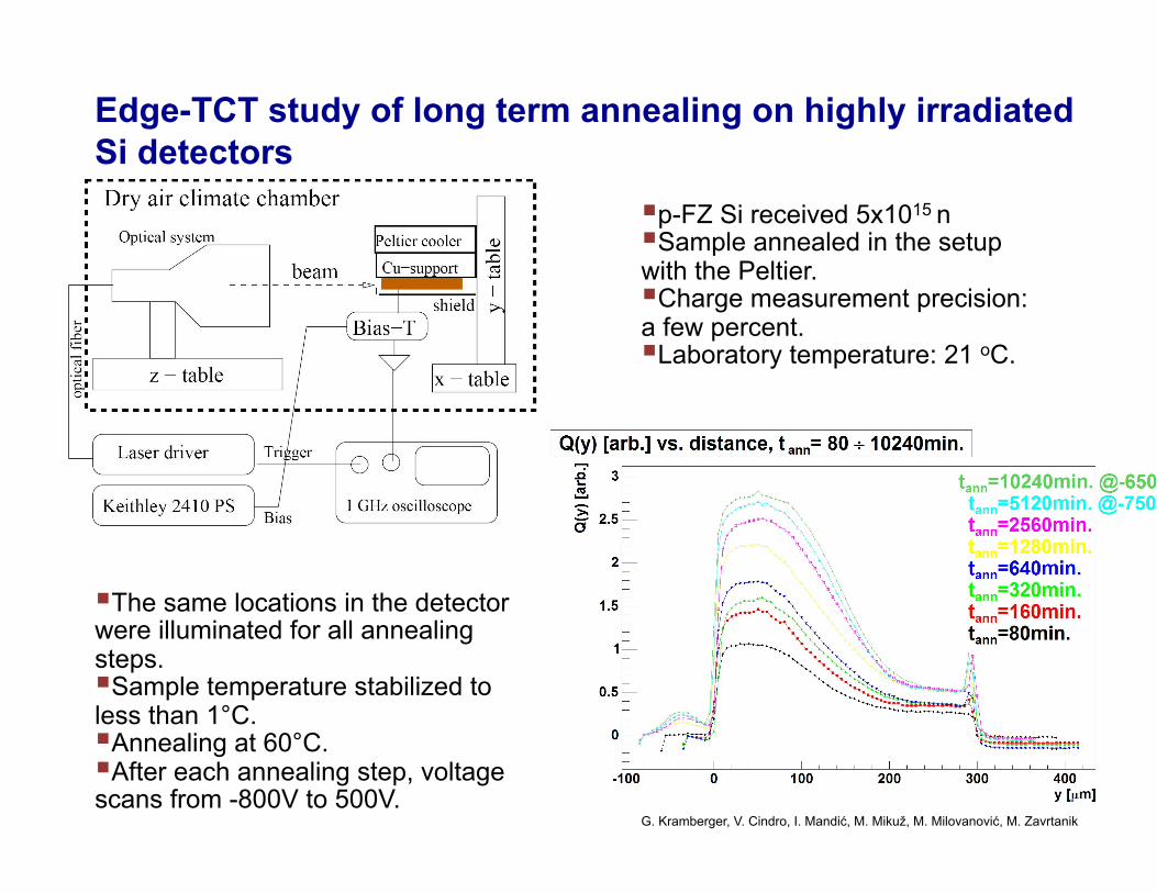
Edge-TCT study of long term annealing on highly irradiated Si detectors
The same locations in the detector were illuminated for all annealing steps. Sample temperature stabilized to less than 1°C. Annealing at 60°C. After each annealing step, voltage scans from -800V to 500V.
G. Kramberger, V. Cindro, I. Mandić, M. Mikuž, M. Milovanović, M. Zavrtanik
p-FZ Si received 5x10¹⁵ n Sample annealed in the setup with the Peltier. Charge measurement precision: a few percent. Laboratory temperature: 21 oC.

25
A. Affolder, G. Casse, P. Allport
Charge collection efficiencies of n-in-p planar sensors after n, p, and π irradiation
Corrected for annealing for pions and 24 GeV p
Charge collected by n-in-p FZ Si may be sufficient at innermost layer.

26
Guard ring design for n-on-p
Synopsis Sentaurus used to predict electric field profile / breakdown voltage for various implant/oxide/metal/passivation configurations. Result sustains Vbias = 900 V for ϕ = 1015 cm-2 neq and Qox < 1012 cm-2.
Example optimizations
O. Koybasi

27
p- versus n-type, Float Zone versus Magnetic Czochralski
J. Metcalfe, M. Hoeferkamp, S. Seidel
Beneficial annealing observed for the first 80 minutes anneal time, then Vfd begins to increase for samples shown to have neg space charge after proton irradiation:
n-on-p Fz
p-on-n Fz
n-on-p MCz
p-on-n MCz shows annealing behavior typical of n-type devices that have +sc after proton irradiation.
A study of Vfull dep after p irradiation and annealing
n-on-p Fz p-on-n Fz n-on-p MCz p-on-n MCz
Manufacturer HPK Micron Micron MicronResistivity 13 kΩ-cm 3.3 kΩ-cm 1.9 kΩ-cm 1.4 kΩ-cmActive Area 3mmx3mm 3mmx3mm 3mmx3mm 3mmx3mmThickness 300 µm 300 µm 300 µm 300 µmInitial Vfd [V] 75 95 520 220
800 MeV p @Los Alamos 60° C anneal
J. Metcalfe, M. Hoeferkamp, S. Seidel

28
p- versus n-type, Float Zone versus Magnetic Czochralski, continued
J. Metcalfe, M. Hoeferkamp, S. Seidel
FZ show greatest increase of Vfd with increasing fluence
n-on-p MCz shows little change

29
CCE versus annealing of p-in-n sensors Motivations: An examination of results for long annealing times, to reduce dependence upon model-based extrapolations; to acquire signal data after high dose and long annealing times, in the regime where CV-based models predict under-depletion.
A. Affolder, H. Brown, G. Casse, P. Dervan, J. Vossebeld, C. Wiglesworth
Vbias = 600 V
Even when the CV-based models predict significant under-depletion, the signal is still sizeable and diminishes only slowly.
FZ, 2x1014 cm-2 neq @ Ljubljana
Models: ATLAS TDR 5 CERN/LHCC/97-17. Hamburg model, thesis of M. Moll, 1999.

30
Lorentz angle in silicon strip sensors
W. de Boer, A. Dierlamm, A. Sabellek, M. Schmanau, M. Schneider
Red laser: best signal IR laser: MIP-like
23 MeV p (Karlsruhe) Magnet up to 8 T
31
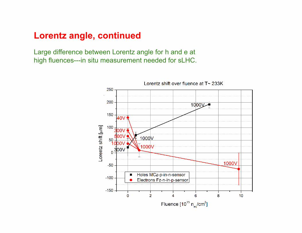
Lorentz angle, continued
Large difference between Lorentz angle for h and e at high fluences---in situ measurement needed for sLHC.

32
Simulation of the electron and hole contributions to total charge collection in irradiated Si detectors
Contribution of holes to total collected charge increases with fluence in an n+ segmented Si detector. At 1x10¹⁶ neq/cm2, contribution of holes to total collected charge is comparable to that of electrons. At sLHC fluences, total collected charge is approximately To improve radiation hardness, carrier trapping distance has to be increased --- e.g. by pre-filling of the traps or decreasing carrier drift distance (3D).
€
Q = 80e /µm ⋅ (dCCEe + dCCE
h )
For P ≥ 60 µm, hole contribution is ~43% due to P >> dCCE or dt
For P < 60 µm, hole contribution decreases as P approaches dCCE or dt.
Zheng Li

33
Sensors with 3D geometry
Motivation: decouple thickness from charge collection distance
Planar 3D

34
Sensors with 3D geometry
RD50 is examining designs by: FBK (Trento) and CNM (Barcelona):
-Columns unfilled -Ohmic columns connected by uniform n+-doping layer and metallization -AC and DC coupled readout pads
-Columns partially filled with polysilicon -Ohmic columns connected by polysilicon and metallization -DC coupled readout pads

35
FBK‐irstSensorswith3DgeometryFordetailspleaseseetalkbyPerHansson.3D‐DoublesideDoubleTypeColumn:“ATLAS3D‐DDTC”
First results show good performance in lab and beam test.
M. Boscardin, G.-F. Dalla Betta, G. Darbo, C. Gemme, A. La Rosa, H. Pernegger, C. Piemonte, M. Povoli, S. Ronchin, A. Zoboli, N. Zorzi

36
Glasgow/CNMSensorswith3DgeometryFordetailspleaseseetalkbyGiulioPellegrini.
First results show good performance in lab and beam test.
R. Bates, C. Parkes, D. Pennicard, B. Rakotomiaramanana, L. Allanelli, C. Fleta, G. Pellegrini, M. Lozano, U. Parzefll, X. Plot, J. Härkönen, E. Tuovinen

37
Simulation, Laboratory, and Test Beam Studies of CMS 3D (SINTEF) sensors
Columns become dead regions at Φ > 1014neq cm-2
CCE highest between electrodes (~ 9 ke- at Φ = 1016neqcm-2 ), lowest near cell edges (~ 5.5 ke- at Φ = 1016neq/cm2 ) ● 2 columns per cell: lower capacitance between readout electrodes (~0.7fF at Φ=0, Qox=4x1011cm-2) less dead volume (~ 4% of total volume) ● 4 columns per cell: faster charge collection less trapping at high fluences lower depletion voltage higher breakdown voltage larger capacitance between readout electrodes (~3.2fF at Φ=0, Qox=4x1011cm-2) larger dead volume (~ 8% of total volume) O. Koybasi, D. Bortoletto, G. Bolla
38
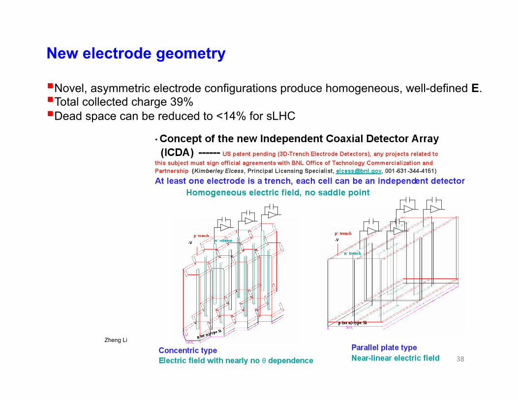
New electrode geometry
Novel, asymmetric electrode configurations produce homogeneous, well-defined E. Total collected charge 39% Dead space can be reduced to <14% for sLHC
Zheng Li

39
Summary
Major advances have been made in correlation of microscopic defect properties with observed material properties.
New information is provided on epitaxial, Czochralski, and p-bulk silicon substrates.
Work is ongoing to understand and optimize Lorentz angle, guard rings, and other design features.
New geometries including 3D and Independent Coaxial Detector Array continue to evolve.


