
NSi1311 High Reliability Reinforced
Isolated Amplifier Datasheet (EN) 1.0
Copyright © 2020, NOVOSENSE
Page 1
Product Overview NSI1311 is a high-performance isolated amplifier with
output separated from input based on the NOVOSENSE
capacitive isolation technology. The device has a single-
ended input signal range from 0.1V to 2V. The high input
impedance of NSI1311 makes it highly suitable for
connection to high-voltage resistive dividers or other
voltage signal sources with high output resistance.
The device has a fixed gain of 1 and provides a differential
analog output.
The low offset and gain drift ensure the accuracy over the
entire temperature range. The high common-mode
transient immunity ensures that the device is able to
provide accurate and reliable measurements even in the
presence of high-power switching such as in motor control
applications.
The fail-safe function (missing VDD1 detection) simplifies
system-level design and diagnostics.
Key Features
Up to 5000Vrms Insulation voltage
0.1~2V, High-Impedance Input Voltage Range
Fixed Gain: 1
Low Offset Error and Drift:
±1.5mV (Max), -5~30μV/ (Max)
Low Gain Error and Drift:
±0.3% (Max), ±45ppm/ (Max)
Low Nonlinearity and Drift:
±0.04% (Max), ±1ppm/ (Typ)
SNR: 82dB (Typ, BW=10kHz), 70dB (Typ, BW=100kHz)
Wide bandwidth: 400kHz (Typ)
High CMTI: 150kV/μs (Typ)
System-Level Diagnostic Feature:
VDD1 monitoring
Operation Temperature: -40~125
RoHS-Compliant Packages:
SOP-8(300mil)
Safety Regulatory Approvals
UL recognition: up to 5000Vrms for 1 minute per UL1577
CQC certification per GB4943.1-2011
CSA component notice 5A approval IEC60950-1 standard
DIN VDE V 0884-11:2017-01
Applications
Bus voltage monitoring
AC motor controls
Power and solar inverters
Uninterruptible Power Suppliers
Automotive onboard chargers
Device Information Part Number Package Body Size
NSI1311 SOP8(300mil) 5.85mm × 7.50mm
Functional Block Diagrams
Σ-Δ modulator
Iso
lati
on
Ba
rrie
r
ReferenceVDD1 detection
Buffer
VDD1 VDD2
VIN
SHTDN
OUTP
OUTN
Oscillator
Retiming and 4th-
Order Active Low-Pass
Filter
Reference
TX
RX
RX
TX
GND1 GND2
Figure 1. NSi1311 Block Diagram

NSi1311 Datasheet (EN) 1.0
Copyright © 2020, NOVOSENSE
Page 2
INDEX
1. PIN CONFIGURATION AND FUNCTIONS ............................................................................................................................... 3
2. ABSOLUTE MAXIMUM RATINGS .......................................................................................................................................... 4
3. RECOMMENDED OPERATING CONDITIONS ......................................................................................................................... 4
4. THERMAL INFORMATION .................................................................................................................................................... 4
5. SPECIFICATIONS .................................................................................................................................................................. 4
5.1. ELECTRICAL CHARACTERISTICS .......................................................................................................................................... 4 5.2. TYPICAL PERFORMANCE CHARACTERISTICS .......................................................................................................................... 6 5.3. PARAMETER MEASUREMENT INFORMATION ........................................................................................................................ 8
6. HIGH VOLTAGE FEATURE DESCRIPTION ............................................................................................................................... 8
6.1. INSULATION AND SAFETY RELATED SPECIFICATIONS ............................................................................................................... 8 6.2. DIN VDE V 0884-11 (VDE V 0884-11): 2017-01 INSULATION CHARACTERISTICS ................................................................... 8 6.3. REGULATORY INFORMATION .......................................................................................................................................... 10
7. FUNCTION DESCRIPTION ................................................................................................................................................... 10
7.1. OVERVIEW ................................................................................................................................................................ 10 7.2. ANALOG INPUT ........................................................................................................................................................... 10 7.3. ANALOG OUTPUT ........................................................................................................................................................ 10
8. APPLICATION NOTE ........................................................................................................................................................... 11
8.1. TYPICAL APPLICATION CIRCUIT ....................................................................................................................................... 11 8.2. SENSE RESISTOR SELECTION ........................................................................................................................................... 12 8.3. PCB LAYOUT .............................................................................................................................................................. 12
9. PACKAGE INFORMATION ................................................................................................................................................... 13
10. ORDERING INFORMATION .............................................................................................................................................. 13
11. DOCUMENTATION SUPPORT ........................................................................................................................................... 13
12. TAPE AND REEL INFORMATION ....................................................................................................................................... 14
13. REVISION HISTORY .......................................................................................................................................................... 15

NSi1311 Datasheet (EN) 1.0
Copyright © 2020, NOVOSENSE Page 3
1. Pin Configuration and Functions
NSI1311TOP VIEW
1VDD1
4GND1
3
2VIN
SHTDN
8 VDD2
5 GND2
6
7 OUTP
OUTN
Figure 1.1 NSi1311 Package
Table 1.1 NSi1311 Pin Configuration and Description
NSi1311 PIN NO.
SYMBOL FUNCTION
1 VDD1 Power supply for isolator side 1(3.0V to 5.5V)
2 VIN Analog input
3 SHTDN Shutdown input, active high, pulled up internally (typical resistor value: 100kΩ)
4 GND1 Ground 1, the ground reference for Isolator Side 1
5 GND2 Ground 2, the ground reference for Isolator Side 2
6 OUTN Negative output
7 OUTP Positive output
8 VDD2 Power supply for isolator side 2 (3.0V to 5.5V)

NSi1311 Datasheet (EN) 1.0
Copyright © 2020, NOVOSENSE Page 4
2. Absolute Maximum Ratings
Parameters Symbol Min Typ Max Unit
Power Supply Voltage VDD1, VDD2 -0.3 6.5 V
Input Voltage VIN GND1-6 VDD1+0.5 V
SHTDN GND1-0.5 VDD1+0.5
Output Voltage OUTP, OUTN GND2-0.5 VDD2+0.5 V
Output current per Output Pin Io -10 10 mA
Operating Temperature TOPR -40 125 °C
Storage Temperature TSTG -55 150 °C
Electrostatic discharge HBM (1) ±2000 V
CDM (2) ±1000 V
(1) Human body model (HBM), per AEC-Q100-002-RevD
(2) Charged device model (CDM), per AEC-Q100-011-RevB
3. Recommended Operating Conditions
Parameters Symbol Min Typ Max Unit
Side1 Power Supply VDD1 3.0 5.0 5.5 V
Side2 Power Supply VDD2 3.0 3.3 5.5 V
Differential input voltage before clipping output VClipping 2.56 V
Linear differential input full scale voltage VFSR 0.1 2 V
Digital input voltage SHTDN GND1 VDD1
Operating Ambient Temperature TA -40 125 °C
4. Thermal Information
Parameters Symbol SOP8(300mil) Unit
Junction–to-ambient thermal resistance RθJA 86 °C/W
Junction-to-case (top) thermal resistance RθJC(top) 28 °C/W
Junction-to-board thermal resistance RθJB 42 °C/W
Junction–to-top characterization parameter ΨJT 4 °C/W
Junction-to-board characterization parameter ΨJB 42 °C/W
5. Specifications
5.1. Electrical Characteristics
(VDD1 = 3.0V~5.5V, VDD2 = 3.0V~5.5V, VIN = 0.1V to 2V, and SHTDN = GND1 = 0V, TA = -40 to 125. Unless otherwise noted, Typical
values are at VDD1 = 5V, VDD2 = 3.3V, TA = 25)

NSi1311 Datasheet (EN) 1.0
Copyright © 2020, NOVOSENSE Page 5
Parameters Symbol Min Typ Max Unit Comments
Power Supply
Side1 Supply Voltage VDD1 3.0 5.0 5.5 V
Side2 Supply Voltage VDD2 3.0 3.3 5.5 V
Side1 Supply Current IDD1 11.4 15.1 mA SHTDN = LOW
1 μA SHTDN = HIGH
Side2 Supply Current IDD2 6.3 8.4 mA
VDD1 undervoltage detection threshold voltage
VDD1UV 1.8 2.3 2.7 V VDD1 falling
Analog Input
Input offset voltage VOS -1.5 ±0.4 1.5 mV VIN = 1V
Input offset drift TCVOS -5 10 30 μV/°C
Input resistance RIN 1 GΩ
Input capacitance CIN 7 pF fIN = 275kHz
Input bias current IIB -15 3.5 15 nA VIN = GND1
Input bias current drift TCIIB ±10 pA/°C
Analog Output
Nominal Gain 1 V/V
Gain error EG -0.3% ±0.05% 0.3%
Gain error thermal drift TCEG -45 ±5 45 ppm/°C
Nonlinearity -0.04% ±0.01% 0.04%
Nonlinearity drift ±1 ppm/°C
Total harmonic distortion THD -87 dB VIN = 1.8V, fIN = 10kHz, BW = 100kHz
Output noise 210 µVRMS VIN = 1V, BW = 100kHz
Signal to noise ratio SNR
78 82 dB VIN = 1.8V, fIN = 1kHz, BW = 10kHz
70 dB VIN = 1.8V, fIN = 10kHz, BW = 100kHz
Common-mode output voltage VCMout 1.36 1.4 1.45 V
Failsafe differential output voltage
VFAILSAFE -2.53 -2.44 V SHTDN active, or VDD1 missing
Output Bandwidth BW 400 kHz
Power supply rejection ratio (1)
PSRRdc -78 dB PSRR vs VDD1, at DC
PSRRac -75 dB PSRR vs VDD1, 100mV and 10kHz ripple

NSi1311 Datasheet (EN) 1.0
Copyright © 2020, NOVOSENSE Page 6
Parameters Symbol Min Typ Max Unit Comments
PSRRdc -82 dB PSRR vs VDD2, at DC
PSRRac -74 dB PSRR vs VDD2, 100mV and 10kHz ripple
Output resistance ROUT <0.2 Ω
Common-mode transient immunity
CMTI 100 150 kV/μs Common-mode transient immunity
Digital Input (SHTDN)
Input current IIN -70 1 µA GND1 ≤ VSHTDN ≤ VDD1
Input capacitance CIN 5 pF
High-level input voltage VIH 0.7*VD
D1
VDD1+0.3
V
Low-level input voltage VIL -0.3 0.3*VD
D1 V
Timing
Rising time of OUTP, OUTN tr 1.3 μs
Falling time of OUTP, OUTN tf 1.3 μs
INP, INN to OUTP, OUTN signal delay (50% - 50%)
tPD 1.6 2.1 μs
Analog setting time tAS 0.5 ms VDD1 step to 3.0 V with VDD2 ≥ 3.0 V, to OUTP, OUTN valid, 0.1% settling
Device enable time tEN 80 100 μs SHTDN high to low
Shutdown time tSHTDN 1.2 5 μs SHTDN low to high
(1) Input referred.
5.2. Typical Performance Characteristics
Unless otherwise noted, test at VDD1 = 5V, VDD2 = 3.3V, 0.1V to 2V, and SHTDN = GND1 = 0V, fIN = 1kHz, BW = 10kHz.
Figure 5.1 Input Offset Voltage vs Temperature
Figure 5.2 Gain Error vs Temperature

NSi1311 Datasheet (EN) 1.0
Copyright © 2020, NOVOSENSE Page 7
Figure 5.3 Nonlinearity vs Temperature
Figure 5.4 Total Harmonic Distortion vs Temperature
Figure 5.5 Signal-to-Noise Ratio vs Temperature
Figure 5.6 UVLO of VDD1 vs Temperature
Figure 5.7 Output Common-Mode Voltage vs Temperature
Figure 5.8 Fail-Safe Output Voltage vs Temperature
Figure 5.9 Vin to Vout Delay vs Temperature
Figure 5.10 Supply Current vs Supply Voltage
NSi1311 Datasheet (EN) 1.0
Copyright © 2020, NOVOSENSE Page 8
Figure 5.11 Supply Current vs Temperature
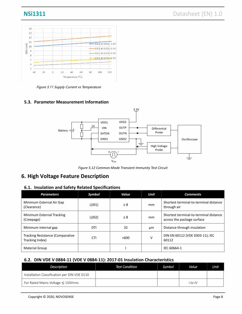
5.3. Parameter Measurement Information
VDD1
SHTDN
VIN
GND1
VDD2
GND2
OUTN
OUTP
3.3V
Oscilloscope
VCM
BatteryDifferential
Probe
High Voltage Probe
1V
Figure 5.12 Common-Mode Transient Immunity Test Circuit
6. High Voltage Feature Description
6.1. Insulation and Safety Related Specifications
Parameters Symbol Value Unit Comments
Minimum External Air Gap (Clearance)
L(I01) ≥ 8 mm Shortest terminal-to-terminal distance through air
Minimum External Tracking (Creepage)
L(I02) ≥ 8 mm Shortest terminal-to-terminal distance across the package surface
Minimum internal gap DTI 32 μm Distance through insulation
Tracking Resistance (Comparative Tracking Index)
CTI >600 V DIN EN 60112 (VDE 0303-11); IEC 60112
Material Group I IEC 60664-1
6.2. DIN VDE V 0884-11 (VDE V 0884-11): 2017-01 Insulation Characteristics
Description Test Condition Symbol Value Unit
Installation Classification per DIN VDE 0110
For Rated Mains Voltage ≤ 150Vrms I to IV

NSi1311 Datasheet (EN) 1.0
Copyright © 2020, NOVOSENSE Page 9
Description Test Condition Symbol Value Unit
For Rated Mains Voltage ≤ 300Vrms I to III
For Rated Mains Voltage ≤ 400Vrms I to III
Climatic Classification 40/125/21
Pollution Degree per DIN VDE 0110,
Table 1 2
Maximum repetitive isolation voltage VIORM 1414 VPEAK
Maximum working isolation voltage AC Voltage
VIOWM 1000 VRMS
DC Voltage 1414 VPEAK
Input to Output Test Voltage, Method B1
VIORM × 1.875 = Vpd (m), 100% production test,
tini = tm = 1 sec, partial discharge < 5 pC
V pd (m) 2652 VPEAK
Input to Output Test Voltage, Method A
After Environmental Tests Subgroup 1 VIORM × 1.5 = Vpd (m), tini = 60 sec, tm =
10 sec, partial discharge < 5 pC V pd (m) 2121 VPEAK
After Input and /or Safety Test Subgroup 2 and Subgroup 3
VIORM × 1.2= Vpd (m), tini = 60 sec, tm = 10 sec, partial discharge < 5 pC
V pd (m) 1697 VPEAK
Maximum transient isolation voltage t = 60 sec VIOTM 8000 VPEAK
Maximum Surge Isolation Voltage Test method per IEC60065,1.2/50us
waveform, VTEST=VIOSM/1.6 VIOSM 6250 VPEAK
Isolation resistance VIO =500V RIO >109 Ω
Isolation capacitance f = 1MHz CIO 0.8 pF
Input capacitance CI 2 pF
Total Power Dissipation at 25°C Ps mW
Safety input, output, or supply current θJA = 140 °C/W, VI = 5.5V, TJ = 150 °C,
TA = 25 °C Is 260 mA
Case Temperature Ts 150 °C
0
50
100
150
200
250
300
0 50 100 150 200
Saf
ety L
imit
ing C
urr
ent
(mA
)
Case Temperature ()

NSi1311 Datasheet (EN) 1.0
Copyright © 2020, NOVOSENSE Page 10
Figure 6.1 NSi1311 Thermal Derating Curve, Dependence of Safety Limiting Values with Case Temperature per DIN VDE V 0884-11
6.3. Regulatory Information
The NSi1311 are approved or pending approval by the organizations listed in table.
UL VDE CQC
UL 1577 Component Recognition Program
Approved under CSA Component Acceptance
Notice 5A
DIN VDE V 0884-11(VDE V 0884-11):2017-01
Certified by CQC11-471543-2012
GB4943.1-2011
Single Protection, 5000Vrms
Isolation voltage Single Protection, 5000Vrms
Isolation voltage Reinforce Insulation
1414Vpeak, VIOSM=6250Vpeak
Basic insulation at 1000VRMS (1414Vpeak)
Reinforced insulation at 400VRMS (565Vpeak)
File (pending) File (pending) File (pending) File (pending)
7. Function Description
7.1. Overview
The NSI1311 is a single-ended, precision, isolated amplifier. The input stage of the device drives a second-order, sigma-delta (ΣΔ) modulator. The modulator uses the internal voltage reference and clock generator to convert the analog input signal to a digital bitstream. The drivers (called TX in the Functional Block Diagram) transfer the output of the modulator across the isolation barrier that separates the side1 and side2 voltage domains. The received bitstream and clock are synchronized and processed, as shown in the Functional Block Diagram, by a fourth-order analog filter on the side2 and presented as a differential output of the device.
SHTDN pin is used to disable the conversion. Since SHTDN is an active high signal and is pulled up by a 100kΩ (typical) internally, it should be connected to GND1 or logic LOW in normal operation.
Σ-Δ modulator
Iso
lati
on
Ba
rrie
r
ReferenceVDD1 detection
Buffer
VDD1 VDD2
VIN
SHTDN
OUTP
OUTN
Oscillator
Retiming and 4th-
Order Active Low-Pass
Filter
Reference
TX
RX
RX
TX
GND1 GND2
Figure 7.1 Function Block Diagram
7.2. Analog Input There are two restrictions on the analog input signal (VIN). If the input voltage exceeds the range GND1 – 6 V to VDD1 + 0.5 V, the input current must be limited to 10 mA because the
device input electrostatic discharge (ESD) diodes turn on. The linearity and noise performance of the device are ensured only when the analog input voltage remains within the specified
linear full-scale range (FSR).
7.3. Analog Output
For linear input range, NSI1311 provides an analog differential output which has a fixed gain of 1. If a full-scale input signal is applied to the NSI1311 (VIN ≥ VClipping), the analog output will be clipped.

NSi1311 Datasheet (EN) 1.0
Copyright © 2020, NOVOSENSE Page 11
In addition, NSI1311 integrates some diagnostic measures and offers a fail-safe output to simplify system-level design. The fail-safe output is a negative differential output voltage that does not occur under normal device operation, and it will only be activated in following conditions:
When the undervoltage of VDD1 is detected (VDD1< VDD1UV).
When SHTDN signal is activated (pulled high).
3.0
2.5
2.0
1.5
1.0
0.5
0
VO
UT
(V)
3.0
2.5
2.0
1.5
1.0
0.5
0
VO
UT
(V)
VFAILSAFE VClipping
OUTP
OUTNOUTP
OUTN
Figure 7.2 Typical Failsafe output and clipping output
8. Application Note
8.1. Typical Application Circuit
NSI1311 has an input impedance of up to 1GΩ, and has a wide input voltage range as well. These features make NSI1311 ideally suitable for isolated voltage sensing applications such as frequency inverters. The typical application circuit is shown in Figure 8.1.
The bus voltage of the frequency inverter is divided by a resistance network, and the divided voltage is applied to the input of NSI1311 through a RC filter. The differential output of the isolated amplifier is converted to a single-ended analog output with an operational-amplifier-based circuit. An analog-to-digital converter usually receives the analog output and converts to digital signal for controller processing.
M
VDD1
VIN
SHTDN
GND1
VDD2
OUTP
OUTN
GND2
VBUS+
VBUS-
NSI1311
3.0~5.5V
3.0~5.5V
To ADC
Rsense
Gate Driver
Gate Driver
Gate Driver
Gate Driver
Gate Driver
Gate Driver
R1
R2
Figure 8.1 Typical application circuit in phase current sensing

NSi1311 Datasheet (EN) 1.0
Copyright © 2020, NOVOSENSE Page 12
8.2. Sense Resistor Selection
There are two other factors should be considered when selecting the sense resistor:
The voltage-drop on Rsense divided by nominal VBUS must not exceed the recommended linear input voltage range: VIN ≤ FSR.
The voltage-drop on Rsense divided by VBUS in maximum allowed overvoltage condition must not exceed the input voltage that causes a clipping output: VIN ≤ VClipping.
8.3. PCB Layout
NSI1311 requires a 0.1µF bypass capacitor between VDD1 and GND1, VDD2 and GND2. The capacitor should be placed as close as possible to the VDD pin. If better filtering is required, an additional 1~10µF capacitor may be used.

NSi1311 Datasheet (EN) 1.0
Copyright © 2020, NOVOSENSE Page 13
9. Package Information
Figure 9.1 SOW8 Package Shape and Dimension in millimeters
10. Ordering Information
Part No. Isolation
Rating(kV)
Linear Input
Range(V)
Moisture Sensitivity
Level Temperature Automotive
Package Type
Package Drawing
SPQ
NSI1311-DSWVR
5 0.1 ~ 2 Level-3 -40 to 125°C NO SOP8
(300mil) SOW8 1000
NSI1311-Q1SWVR
5 0.1 ~ 2 Level-3 -40 to 125°C YES SOP8
(300mil) SOW8 1000
11. Documentation Support
Part Number Product Folder Datasheet Technical Documents Isolator selection guide
NSi1311 Click here Click here Click here Click here
NSi1311 Datasheet (EN) 1.0
Copyright © 2020, NOVOSENSE Page 14
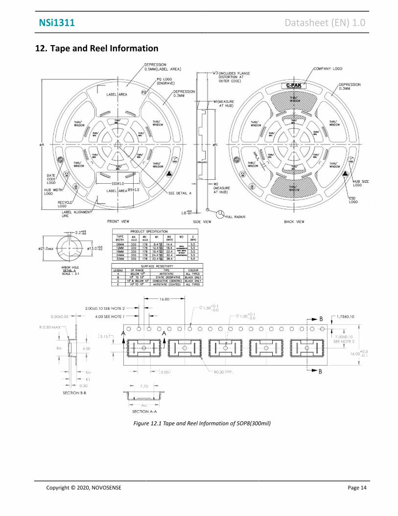
12. Tape and Reel Information
Figure 12.1 Tape and Reel Information of SOP8(300mil)

NSi1311 Datasheet (EN) 1.0
Copyright © 2020, NOVOSENSE Page 15
13. Revision History
Revision Description Date
1.0 Initial Release 2020/8/29


