NINA-B2 series Stand-alone dual-mode Bluetooth modules
System Integration Manual
Abstract
This document describes the system integration of NINA-B2 series stand-alone Bluetooth® modules. The NINA-B2 modules come with pre-flashed application software and support dual-mode Bluetooth (Bluetooth BR/EDR and Bluetooth low energy). The module has many important security features embedded, including secure boot, which ensures that only authenticated software can run on the module. This makes NINA-B2 ideal for critical IoT applications where security is important.
www.u-blox.com
UBX-18011096 - R04
NINA-B2 series - System Integration Manual
UBX-18011096 - R04 Document Information Page 2 of 30
Document Information Title NINA-B2 series
Subtitle Stand-alone dual-mode Bluetooth modules
Document type System Integration Manual
Document number UBX-18011096
Revision and date R04 17-Dec-2019
Disclosure Restriction
Product status Corresponding content status
Functional Sample Draft For functional testing. Revised and supplementary data will be published later.
In Development / Prototype
Objective Specification Target values. Revised and supplementary data will be published later.
Engineering Sample Advance Information Data based on early testing. Revised and supplementary data will be published later.
Initial Production Early Production Information Data from product verification. Revised and supplementary data may be published later.
Mass Production / End of Life
Production Information Document contains the final product specification.
This document applies to the following products:
Product name Type number Software version Hardware version PCN reference Product status
NINA-B221 NINA-B221-xxB-xx All versions 06 N/A Initial Production
NINA-B222 NINA-B222-xxB-xx All versions 06 N/A Initial Production
u-blox or third parties may hold intellectual property rights in the products, names, logos and designs included in this document. Copying, reproduction, modification or disclosure to third parties of this document or any part thereof is only permitted with the express written permission of u-blox.
The information contained herein is provided “as is” and u-blox assumes no liability for its use. No warranty, either express or implied, is given, including but not limited to, with respect to the accuracy, correctness, reliability and fitness for a particular purpose of the information. This document may be revised by u-blox at any time without notice. For the most recent documents, visit www.u-blox.com.
Copyright © u-blox AG.
NINA-B2 series - System Integration Manual
UBX-18011096 - R04 Contents Page 3 of 30
Contents Document Information ................................................................................................................................ 2 Contents .......................................................................................................................................................... 3 1 System description ............................................................................................................................... 5
1.1 Overview ........................................................................................................................................................ 5 1.1.1 Block diagram ...................................................................................................................................... 5
1.2 Product description .................................................................................................................................... 6 1.2.1 Radio in NINA-B2 series ..................................................................................................................... 6
1.3 CPU................................................................................................................................................................. 6 1.4 Operating modes ......................................................................................................................................... 6
1.4.1 Power modes ....................................................................................................................................... 6 1.5 Supply interfaces ........................................................................................................................................ 6
1.5.1 Module supply design (VCC) ............................................................................................................. 6 1.5.2 Digital I/O interfaces reference voltage (VCC_IO) ........................................................................ 6 1.5.3 VCC application circuits .................................................................................................................... 7
1.6 System function interfaces ...................................................................................................................... 7 1.6.1 Boot strapping pins ............................................................................................................................ 7
1.7 Serial Interfaces .......................................................................................................................................... 8 1.7.1 Universal asynchronous serial interface (UART) ......................................................................... 8
1.8 Antenna interfaces ..................................................................................................................................... 9 1.8.1 Antenna pin – NINA-B221 ................................................................................................................. 9 1.8.2 Integrated antenna – NINA-B222 .................................................................................................... 9
1.9 Reserved pins (RSVD) ................................................................................................................................ 9 1.10 GND pins ....................................................................................................................................................... 9
2 Software ................................................................................................................................................ 10 2.1 Flashing the NINA module .......................................................................................................................10 2.2 Updating the NINA-B2 u-blox connectivity software ........................................................................10
3 Design-in ................................................................................................................................................ 12 3.1 Overview ......................................................................................................................................................12 3.2 Supply interfaces ......................................................................................................................................12
3.2.1 Module supply (VCC) design ...........................................................................................................12 3.2.2 Digital I/O interfaces reference voltage (VCC_IO) ......................................................................12
3.3 Antenna interface .....................................................................................................................................13 3.3.1 RF transmission line design (NINA-B221 only) ..........................................................................13 3.3.2 Antenna design (NINA-B221) .........................................................................................................14 3.3.3 On-board antenna design (NINA-B222) .......................................................................................17
3.4 Data communication interfaces ............................................................................................................18 3.4.1 Asynchronous serial interface (UART) design ............................................................................18
3.5 General High Speed layout guidelines ..................................................................................................18 3.5.1 General considerations for schematic design and PCB floor-planning .................................19 3.5.2 Module placement ............................................................................................................................19 3.5.3 Layout and manufacturing .............................................................................................................19
3.6 Module footprint and paste mask .........................................................................................................19
NINA-B2 series - System Integration Manual
UBX-18011096 - R04 Contents Page 4 of 30
3.7 Thermal guidelines ...................................................................................................................................20 3.8 ESD guidelines ...........................................................................................................................................20
4 Handling and soldering ..................................................................................................................... 21 4.1 Packaging, shipping, storage and moisture preconditioning ..........................................................21 4.2 Handling ......................................................................................................................................................21 4.3 Soldering .....................................................................................................................................................21
4.3.1 Reflow soldering process ................................................................................................................21 4.3.2 Cleaning ..............................................................................................................................................22 4.3.3 Other remarks ...................................................................................................................................23
5 Approvals ............................................................................................................................................... 24 5.1 General requirements ..............................................................................................................................24 5.2 FCC/IC End-product regulatory compliance ........................................................................................24
5.2.1 NINA-B2 series FCC ID and IC certification number ..................................................................24 5.2.2 Antenna requirements ....................................................................................................................24
6 Product testing ................................................................................................................................... 26 6.1 u-blox In-Series production test .............................................................................................................26 6.2 OEM manufacturer production test .....................................................................................................26
6.2.1 “Go/No go” tests for integrated devices ......................................................................................27 Appendix ....................................................................................................................................................... 28 Related documents ................................................................................................................................... 29 Revision history .......................................................................................................................................... 29 Contact .......................................................................................................................................................... 30
NINA-B2 series - System Integration Manual
UBX-18011096 - R04 System description Page 5 of 30
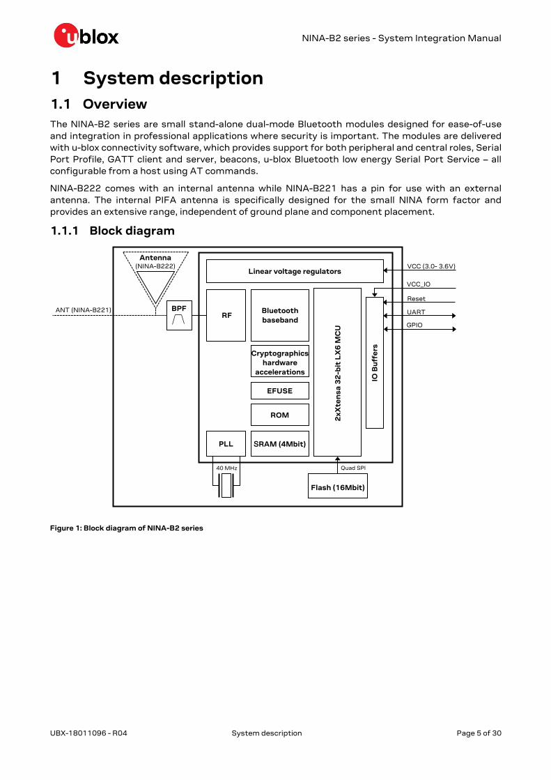
1 System description 1.1 Overview The NINA-B2 series are small stand-alone dual-mode Bluetooth modules designed for ease-of-use and integration in professional applications where security is important. The modules are delivered with u-blox connectivity software, which provides support for both peripheral and central roles, Serial Port Profile, GATT client and server, beacons, u-blox Bluetooth low energy Serial Port Service – all configurable from a host using AT commands.
NINA-B222 comes with an internal antenna while NINA-B221 has a pin for use with an external antenna. The internal PIFA antenna is specifically designed for the small NINA form factor and provides an extensive range, independent of ground plane and component placement.
1.1.1 Block diagram
Figure 1: Block diagram of NINA-B2 series
Flash (16Mbit)
Linear voltage regulators
RF
ROM
IO B
uff
ers
2xX
ten
sa 3
2-b
it L
X6
MC
U
SRAM (4Mbit)
Cryptographics hardware
accelerations
Antenna (NINA-B222)
PLL
Quad SPI
VCC_IO VCC (3.0- 3.6V)
40 MHz
Reset UART
EFUSE
GPIO BPF ANT (NINA-B221) Bluetooth
baseband
NINA-B2 series - System Integration Manual
UBX-18011096 - R04 System description Page 6 of 30
1.2 Product description
1.2.1 Radio in NINA-B2 series
The NINA-B2 series modules support Bluetooth BR/EDR, and Bluetooth Low Energy as explained in Table 1.
Bluetooth BR/EDR Bluetooth low energy
Bluetooth v4.2+EDR
Maximum number of slaves: 7
Bluetooth 4.2 BLE dual-mode
Band support
2.4 GHz, 79 channels
Band support
2.4 GHz, 40 channels
Typical conducted output power - 1 Mbit/s: 6 dBm - 2/3 Mbit/s: 8 dBm
Typical conducted output power
6 dBm
Typical conducted output power - 1 Mbit/s: 6 dBm - 2/3 Mbit/s: 8 dBm
Typical conducted output power
6 dBm
Typical radiated output power
- 1 Mbit: 9 dBm EIRP*
- 2/3 Mbit/s: 11 dBm EIRP*
Typical radiated output power
9 dBm EIRP*
Conducted sensitivity
-88 dBm
Conducted sensitivity
-88 dBm
Data rates:
1 / 2 / 3 Mbit/s
Data rates:
1 Mbit/s
* RF power including maximum antenna gain (3 dBi).
Table 1: NINA-B2 series - Bluetooth characteristics
1.3 CPU The NINA-B2 series has a dual-core system with two Harvard Architecture Xtensa LX6 CPUs with maximum 240 MHz internal clock frequency. The internal memory of NINA-B2 includes the following:
• 448 Kbyte ROM for booting and core functions • 520 Kbyte SRAM for data and instruction • 16 Mbit FLASH for code storage including hardware encryption to protect programs and
data • 1 kbit EFUSE (non- erasable memory) for MAC addresses, module configuration, Flash-
Encryption, and Chip-ID
1.4 Operating modes
1.4.1 Power modes
The NINA-B2 series modules are power efficient devices capable of operating in different power saving modes and configurations. Different sections of the module can be powered off when not needed and complex wake up events can be generated from different external and internal inputs.
1.5 Supply interfaces
1.5.1 Module supply design (VCC)
The NINA-B2 series modules use an integrated Linear Voltage converter to transform the supply voltage presented at the VCC pin into a stable system voltage.
1.5.2 Digital I/O interfaces reference voltage (VCC_IO)
NINA-B2 series - System Integration Manual
UBX-18011096 - R04 System description Page 7 of 30
All modules in the NINA-B2 series provide an additional voltage supply input for setting the I/O voltage level.
The separate VCC_IO pin enables integration of the module in many applications with different voltage levels (for example, 1.8 V or 3.3 V) without any level converters. The NINA-B2 modules support only 3.3 V as IO voltage level currently.
1.5.3 VCC application circuits
The power for the NINA-B2 series modules is provided through the VCC pins, which can be one of the following:
• Switching Mode Power Supply (SMPS) • Low Drop Out (LDO) regulator
The SMPS is the ideal choice when the available primary supply source has higher value than the operating supply voltage of the NINA-B2 series modules. The use of SMPS provides the best power efficiency for the overall application and minimizes current drawn from the main supply source.
While selecting SMPS, ensure that AC voltage ripple at switching frequency is kept as low as possible. Layout shall be implemented to minimize impact of high frequency ringing.
The use of an LDO linear regulator is convenient for a primary supply with a relatively low voltage where the typical 85-90% efficiency of the switching regulator leads to minimal current saving. Linear regulators are not recommended for high voltage step-down as they will dissipate a considerable amount of energy.
DC/DC efficiency should be evaluated as a tradeoff between active and idle duty cycle of the specific application. Although some DC/DC can achieve high efficiency at extremely light loads, a typical DC/DC efficiency quickly degrades as idle current drops below a few mA greatly reducing the battery life.
It is considered as a best practice to have decoupling capacitors on the supply rails close to the NINA-B2 series module, although depending on the design of the power routing on the host system, capacitance might not be needed.
See the NINA-B2 series Data Sheet [2] for electrical specifications.
1.6 System function interfaces
1.6.1 Boot strapping pins
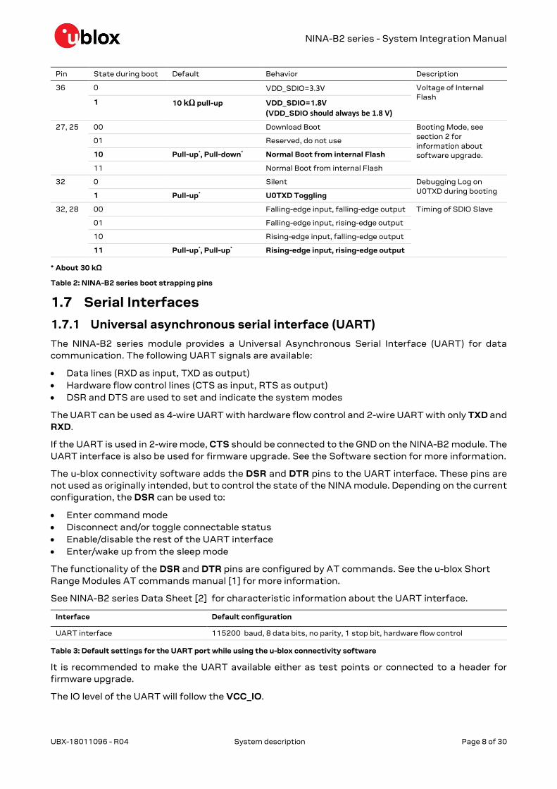
There are several boot configuration pins available on the module that must have the correct settings during boot. It is important that they are in the default state (marked with bold in Table 2) during startup for normal operation. The default state is automatically selected (with internal pull-ups or pull-downs) if the pins are left unconnected.
NINA-B2 series - System Integration Manual
UBX-18011096 - R04 System description Page 8 of 30
Pin State during boot Default Behavior Description
36 0 VDD_SDIO=3.3V Voltage of Internal Flash
1 10 kΩ pull-up VDD_SDIO=1.8V (VDD_SDIO should always be 1.8 V)
27, 25 00 Download Boot Booting Mode, see section 2 for information about software upgrade.
01 Reserved, do not use
10 Pull-up*, Pull-down* Normal Boot from internal Flash
11 Normal Boot from internal Flash
32 0 Silent Debugging Log on U0TXD during booting 1 Pull-up* U0TXD Toggling
32, 28 00 Falling-edge input, falling-edge output Timing of SDIO Slave
01 Falling-edge input, rising-edge output
10 Rising-edge input, falling-edge output
11 Pull-up*, Pull-up* Rising-edge input, rising-edge output
* About 30 kΩ
Table 2: NINA-B2 series boot strapping pins
1.7 Serial Interfaces
1.7.1 Universal asynchronous serial interface (UART)
The NINA-B2 series module provides a Universal Asynchronous Serial Interface (UART) for data communication. The following UART signals are available:
• Data lines (RXD as input, TXD as output) • Hardware flow control lines (CTS as input, RTS as output) • DSR and DTS are used to set and indicate the system modes
The UART can be used as 4-wire UART with hardware flow control and 2-wire UART with only TXD and RXD.
If the UART is used in 2-wire mode, CTS should be connected to the GND on the NINA-B2 module. The UART interface is also be used for firmware upgrade. See the Software section for more information.
The u-blox connectivity software adds the DSR and DTR pins to the UART interface. These pins are not used as originally intended, but to control the state of the NINA module. Depending on the current configuration, the DSR can be used to:
• Enter command mode • Disconnect and/or toggle connectable status • Enable/disable the rest of the UART interface • Enter/wake up from the sleep mode
The functionality of the DSR and DTR pins are configured by AT commands. See the u-blox Short Range Modules AT commands manual [1] for more information.
See NINA-B2 series Data Sheet [2] for characteristic information about the UART interface.
Interface Default configuration
UART interface 115200 baud, 8 data bits, no parity, 1 stop bit, hardware flow control
Table 3: Default settings for the UART port while using the u-blox connectivity software
It is recommended to make the UART available either as test points or connected to a header for firmware upgrade.
The IO level of the UART will follow the VCC_IO.
NINA-B2 series - System Integration Manual
UBX-18011096 - R04 System description Page 9 of 30
1.8 Antenna interfaces The antenna interface is different for each module variant in the NINA-B2 series.
1.8.1 Antenna pin – NINA-B221
The NINA-B221 modules are equipped with an RF pin. The RF pin has a nominal characteristic impedance of 50 Ω and must be connected to the antenna through a 50 Ω transmission line to allow reception of radio frequency (RF) signals in the 2.4 GHz frequency band.
Choose an antenna with optimal radiating characteristics for the best electrical performance and overall module functionality. An internal antenna, integrated on the application board or an external antenna that is connected to the application board through a proper 50 Ω connector can be used.
While using an external antenna, the PCB-to-RF-cable transition must be implemented using either a suitable 50 Ω connector, or an RF-signal solder pad (including GND) that is optimized for 50 Ω characteristic impedance.
1.8.1.1 Antenna matching
The antenna return loss should be as good as possible across the entire band when the system is operational to provide optimal performance. The enclosure, shields, other components, and surrounding environment will impact the return loss seen at the antenna port. Matching components are often required to retune the antenna to bring the return loss within an acceptable range.
It is difficult to predict the actual matching values for the antenna in the final form factor. Therefore, it is a good practice to have a placeholder in the circuit with a ”pi” network, with two shunt components and a series component in the middle, to allow maximum flexibility while tuning the matching to the antenna feed.
1.8.1.2 Approved antenna designs
NINA-B2 modules come with a pre-certified design that can be used to save costs and time during the certification process. To take advantage of this service, you have to implement the antenna layout according to the u-blox reference designs. The reference design is available on request from u-blox.
The designer integrating a u-blox reference design into an end-product is solely responsible for the unintentional emission levels produced by the end product.
The module may be integrated with other antennas. In this case, the OEM installer must certify his design with respective regulatory agencies.
1.8.2 Integrated antenna – NINA-B222
The NINA-B222 modules are equipped with an integrated antenna on the module for simpler integration.
1.9 Reserved pins (RSVD) RSVD pins should be left unconnected.
1.10 GND pins Good connection of the module's GND pins with solid ground layer of the host application board is required for correct RF performance. It significantly reduces the EMC issues and provides a thermal heat sink for the module.
NINA-B2 series - System Integration Manual
UBX-18011096 - R04 Software Page 10 of 30
2 Software The NINA-B2 series module is delivered with the u-blox connectivity software.
The u-blox connectivity software enables the use of Bluetooth, controlled by the AT commands over the UART interface. For more information on the features and capabilities of the u-blox connectivity software and how to use it, see the u-blox Short Range Modules AT Commands Manual [1] and NINA-B2 Getting Started [4].
2.1 Flashing the NINA module The NINA-B2 application can be flashed using the s-center (XMODEM protocol is used). The following pins should be made available as either headers or test points to flash the module:
• UART (RXD, TXD, CTS, RTS) • Bootstrap pins 25 and 27 • Reset_n • SWITCH_1 and SWITCH_2
2.2 Updating the NINA-B2 u-blox connectivity software The u-blox connectivity software for NINA-B2 is designed to validate the hardware, bootloader, and the binary image itself to make sure it runs only on a validated hardware such as NINA-B2.
The u-blox connectivity software is delivered in a zip file – “NINA-B22X-xxx.zip”.
Unzip this file before downloading. The secure boot is included in the file – “NINA-B2-Secureboot.json”.
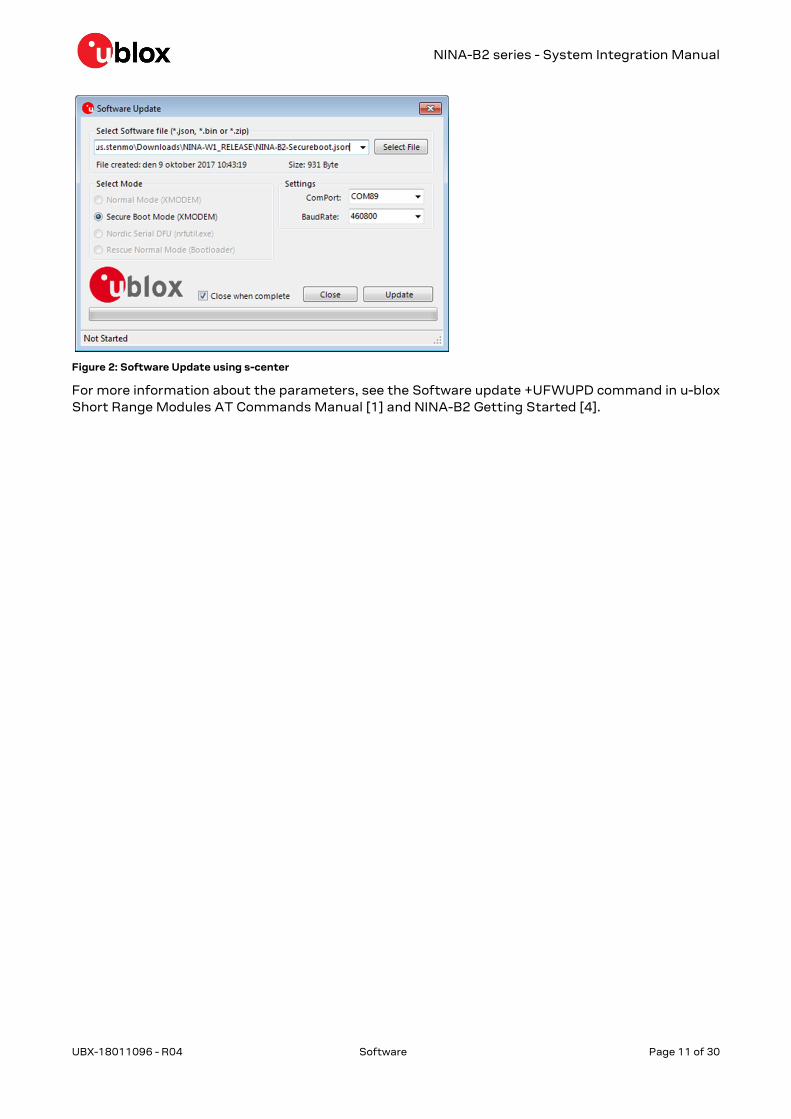
In the s-center software, secure boot is supported from version 4.7 onwards. The *.json-file should be selected to make to use secure boot in the s-center as shown in Figure 2.
The s-center will handle the download using the information in the *.json file. No other interaction is needed from the user.
To manually start the download using a software other than s-center, use the following AT command to start updating the NINA-B2 u-blox connectivity software:
AT+UFWUPD=<mode>,<baud>,<image id>,<image size>,<base64 encoded signature>,<image name>,<flags>
Sample parameters that can be used while doing the flash update is provided below:
AT+UFWUPD=0,115200,0,651840,jzlRIkg37ir/pVpDKVrPot2ZdsaNvUtSYP2pDAUVJc7iQI9yzIo8VFv8C1olP/9I4UJ4WmgC5oRay4AC0V8jRJSFFX/wop6x/sBJGOeDEu7yC/s0+Oj7CLs4TzNbiRqK0zLwKRiHohgVyzWqhwKFpmcxcDXphjkCTIvpffY8TwDLzkowuuD59R+sQCueJtBHBg9KDB3TOs8bsXLaVtT2x1rLfMg8/pb+BPQEK9NcNB4hbp693ATivYE3cmxzWykIjEje819SIRGhHFt0wAsqh7WFgSJYNgDi5cLdOYz+r1+j7+l4RqrMl/A/QYyWS9z0Q15QcJ3GlAJlXYa5v/ISjA==,nina-b2-debug,rwx
When a ‘C’ character is received from NINA-B2, the XMODEM download is ready to begin from the host.
NINA-B2 series - System Integration Manual
UBX-18011096 - R04 Software Page 11 of 30
Figure 2: Software Update using s-center
For more information about the parameters, see the Software update +UFWUPD command in u-blox Short Range Modules AT Commands Manual [1] and NINA-B2 Getting Started [4].
NINA-B2 series - System Integration Manual
UBX-18011096 - R04 Design-in Page 12 of 30
3 Design-in 3.1 Overview For an optimal integration of NINA-B2 series modules in the final application board, it is recommended to follow the design guidelines stated in this chapter. Every application circuit must be properly designed to guarantee the correct functionality of the related interface, however a number of points require high attention during the design of the application device.
The following list provides important points sorted by rank of importance in the application design, starting from the highest relevance:
1. Module antenna connection: Ant pad Antenna circuit affects the RF compliance of the device integrating NINA-B221 modules with applicable certification schemes. Follow the recommendations provided in section 3.3 for schematic and layout design.
2. Module supply: VCC, VCC_IO, and GND pins The supply circuit affects the performance of the device integrating NINA-B2 series module. Follow the recommendations provided in section 3.2 for schematic and layout design.
3. High speed interfaces: UART pins High speed interfaces can be a source of radiated noise and can affect compliance with regulatory standards for radiated emissions. Follow the recommendations provided in section 3.4.1 for schematic and layout design.
4. System functions: RESET_N, GPIO and other System input and output pins Accurate design is required to guarantee that the voltage level is well defined during module boot. Other pins: Accurate design is required to guarantee proper functionality.
3.2 Supply interfaces
3.2.1 Module supply (VCC) design
Good connection of the module’s VCC pin with DC supply source is required for correct RF performance. The guidelines are summarized below:
• The VCC connection must be as wide and short as possible. • The VCC connection must be routed through a PCB area separated from sensitive analog
signals and sensitive functional units. It is a good practice to interpose at least one layer of the PCB ground between VCC track and other signal routing.
There is no strict requirement of adding bypass capacitance to the supply net close to the module. But depending on the layout of the supply net and other consumers on the same net, bypass capacitors might still be beneficial. Though the GND pins are internally connected, connect all the available pins to solid ground on the application board, as a good (low impedance) connection to an external ground can minimize power loss and improve RF and thermal performance.
3.2.2 Digital I/O interfaces reference voltage (VCC_IO)
Good connection of the module’s VCC_IO pin with DC supply source is required for correct performance. The guidelines are summarized below:
• The VCC_IO connection must be as wide and short as possible. • The VCC_IO connection must be routed through a PCB area separated from sensitive analog
signals and sensitive functional units. It is a good practice to interpose at least one layer of PCB ground between VCC_IO track and other signal routing.
There is no strict requirement of adding bypass capacitance to the supply net close to the module. But depending on the layout of the supply net and other consumers on the same net, bypass capacitors might still be beneficial. Though the GND pins are internally connected, connect all the
NINA-B2 series - System Integration Manual
UBX-18011096 - R04 Design-in Page 13 of 30
available pins to solid ground on the application board, as a good (low impedance) connection to an external ground can minimize power loss and improve RF and thermal performance.
3.3 Antenna interface As the unit cannot be mounted arbitrarily, the placement should be chosen with consideration so that it does not interfere with radio communication. The NINA-B222 modules with an internal surface mounted antenna cannot be mounted in a metal enclosure. No metal casing or plastics using metal flakes should be used. Avoid metallic based paint or lacquer as well. The NINA-B222 modules offer more freedom as an external antenna can be mounted further away from the module.
According to the FCC regulations, the transmission line from the module’s antenna pin to the antenna or antenna connector on the host PCB is considered part of the approved antenna design. Therefore, module integrators must either follow exactly one of the antenna reference design used in the module’s FCC type approval or certify their own designs.
3.3.1 RF transmission line design (NINA-B221 only)
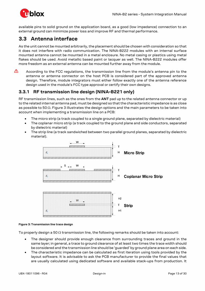
RF transmission lines, such as the ones from the ANT pad up to the related antenna connector or up to the related internal antenna pad, must be designed so that the characteristic impedance is as close as possible to 50 Ω. Figure 3 illustrates the design options and the main parameters to be taken into account when implementing a transmission line on a PCB:
• The micro strip (a track coupled to a single ground plane, separated by dielectric material) • The coplanar micro strip (a track coupled to the ground plane and side conductors, separated
by dielectric material) • The strip line (a track sandwiched between two parallel ground planes, separated by dielectric
material).
Figure 3: Transmission line trace design
To properly design a 50 Ω transmission line, the following remarks should be taken into account:
• The designer should provide enough clearance from surrounding traces and ground in the same layer; in general, a trace to ground clearance of at least two times the trace width should be considered and the transmission line should be ‘guarded’ by ground plane area on each side.
• The characteristic impedance can be calculated as first iteration using tools provided by the layout software. It is advisable to ask the PCB manufacturer to provide the final values that are usually calculated using dedicated software and available stack-ups from production. It
NINA-B2 series - System Integration Manual
UBX-18011096 - R04 Design-in Page 14 of 30
could also be possible to request an impedance coupon on panel’s side to measure the real impedance of the traces.
• FR-4 dielectric material, although its high losses at high frequencies can be considered in RF designs provided that:
o RF trace length must be minimized to reduce dielectric losses. o If traces longer than few centimeters are needed, it is recommended to use a coaxial
connector and cable to reduce losses o Stack-up should allow for thick 50 Ω traces and at least 200 µm trace width is
recommended to assure good impedance control over the PCB manufacturing process. o FR-4 material exhibits poor thickness stability and thus less control of impedance over
the trace length. Contact the PCB manufacturer for specific tolerance of controlled impedance traces.
• The transmission lines width and spacing to the GND must be uniform and routed as smoothly as possible: route RF lines in 45 °C angle or in arcs.
• Add GND stitching vias around transmission lines.
• Ensure solid metal connection of the adjacent metal layer on the PCB stack-up to main ground layer, providing enough vias on the adjacent metal layer.
• Route RF transmission lines far from any noise source (as switching supplies and digital lines) and from any sensitive circuit to avoid crosstalk between RF traces and Hi-impedance or analog signals.
• Avoid stubs on the transmission lines, any component on the transmission line should be placed with the connected pad over the trace. Also avoid any unnecessary component on RF traces.
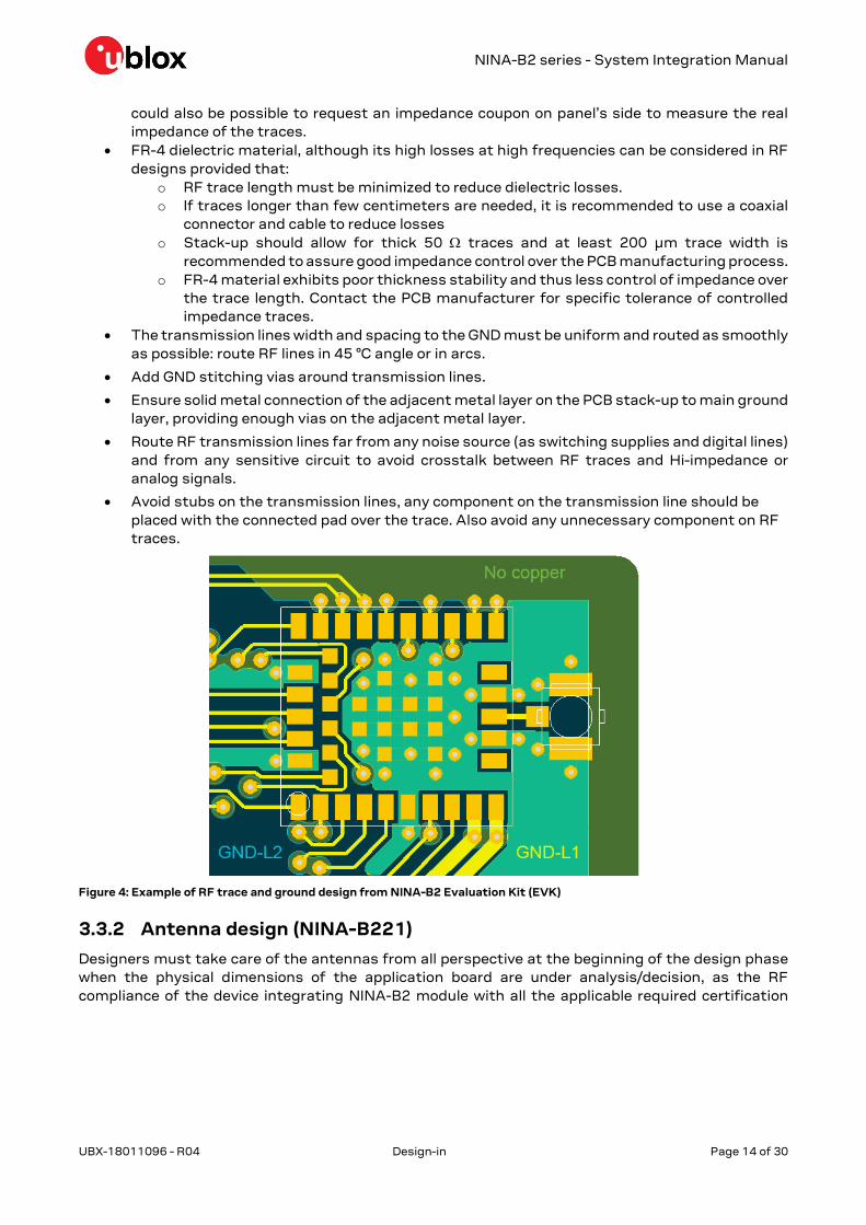
Figure 4: Example of RF trace and ground design from NINA-B2 Evaluation Kit (EVK)
3.3.2 Antenna design (NINA-B221)
Designers must take care of the antennas from all perspective at the beginning of the design phase when the physical dimensions of the application board are under analysis/decision, as the RF compliance of the device integrating NINA-B2 module with all the applicable required certification
NINA-B2 series - System Integration Manual
UBX-18011096 - R04 Design-in Page 15 of 30
schemes heavily depends on the radiating performance of the antennas. The designer is encouraged to consider one of the u-blox suggested antenna part numbers and follow the layout requirements.
• External antennas such as linear monopole:
o External antennas basically do not imply physical restriction to the design of the PCB where the module is mounted.
o The radiation performance mainly depends on the antennas. It is required to select antennas with optimal radiating performance in the operating bands.
o RF cables should be carefully selected with minimum insertion losses. Additional insertion loss will be introduced by low quality or long cable. Large insertion loss reduces radiation performance.
o A high quality 50 Ω coaxial connector provides proper PCB-to-RF-cable transition.
• Integrated antennas such as patch-like antennas:
o Internal integrated antennas imply physical restriction to the PCB design:
Integrated antenna excites RF currents on its counterpoise, typically the PCB ground plane of the device that becomes part of the antenna; its dimension defines the minimum frequency that can be radiated. Therefore, the ground plane can be reduced down to a minimum size that should be similar to the quarter of the wavelength of the minimum frequency that has to be radiated, given that the orientation of the ground plane related to the antenna element must be considered.
The RF isolation between antennas in the system has to be as high as possible and the correlation between the 3D radiation patterns of the two antennas has to be as low as possible. In general, an RF separation of at least a quarter wavelength between the two antennas is required to achieve a maximum isolation and low pattern correlation; increased separation should be considered if possible, to maximize the performance and fulfil the requirements in Table 4.
As a numerical example, the physical restriction to the PCB design can be considered as shown below:
Frequency = 2.4 GHz Wavelength = 12.5 cm Quarter wavelength = 3.125 cm1
o Radiation performance depends on the whole product and antenna system design, including product mechanical design and usage. Antennas should be selected with optimal radiating performance in the operating bands according to the mechanical specifications of the PCB and the whole product.
Table 4 summarizes the requirements for the antenna RF interface:
1 Wavelength referred to a signal propagating over the air.
NINA-B2 series - System Integration Manual
UBX-18011096 - R04 Design-in Page 16 of 30
Item Requirements Remarks
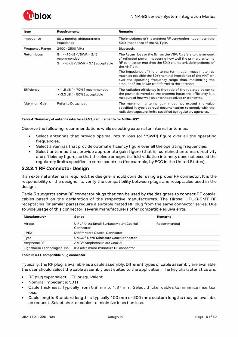
Impedance 50 Ω nominal characteristic impedance
The impedance of the antenna RF connection must match the 50 Ω impedance of the ANT pin.
Frequency Range 2400 - 2500 MHz Bluetooth.
Return Loss S11 < -10 dB (VSWR < 2:1) recommended
S11 < -6 dB (VSWR < 3:1) acceptable
The Return loss or the S11, as the VSWR, refers to the amount of reflected power, measuring how well the primary antenna RF connection matches the 50 Ω characteristic impedance of the ANT pin.
The impedance of the antenna termination must match as much as possible the 50 Ω nominal impedance of the ANT pin over the operating frequency range thus, maximizing the amount of the power transferred to the antenna.
Efficiency > -1.5 dB ( > 70% ) recommended
> -3.0 dB ( > 50% ) acceptable
The radiation efficiency is the ratio of the radiated power to the power delivered to the antenna input; the efficiency is a measure of how well an antenna receives or transmits.
Maximum Gain Refer to Datasheet The maximum antenna gain must not exceed the value specified in type approval documentation to comply with the radiation exposure limits specified by regulatory agencies.
Table 4: Summary of antenna interface (ANT) requirements for NINA-B221
Observe the following recommendations while selecting external or internal antennas:
• Select antennas that provide optimal return loss (or VSWR) figure over all the operating frequencies.
• Select antennas that provide optimal efficiency figure over all the operating frequencies. • Select antennas that provide appropriate gain figure (that is, combined antenna directivity
and efficiency figure) so that the electromagnetic field radiation intensity does not exceed the regulatory limits specified in some countries (for example, by FCC in the United States).
3.3.2.1 RF Connector Design
If an external antenna is required, the designer should consider using a proper RF connector. It is the responsibility of the designer to verify the compatibility between plugs and receptacles used in the design.
Table 5 suggests some RF connector plugs that can be used by the designers to connect RF coaxial cables based on the declaration of the respective manufacturers. The Hirose U.FL-R-SMT RF receptacles (or similar parts) require a suitable mated RF plug from the same connector series. Due to wide usage of this connector, several manufacturers offer compatible equivalents.
Manufacturer Series Remarks
Hirose U.FL® Ultra Small Surface Mount Coaxial Connector
Recommended
I-PEX MHF® Micro Coaxial Connector
Tyco UMCC® Ultra-Miniature Coax Connector
Amphenol RF AMC® Amphenol Micro Coaxial
Lighthorse Technologies, Inc. IPX ultra micro-miniature RF connector
Table 5: U.FL compatible plug connector
Typically, the RF plug is available as a cable assembly. Different types of cable assembly are available; the user should select the cable assembly best suited to the application. The key characteristics are:
• RF plug type: select U.FL or equivalent • Nominal impedance: 50 Ω • Cable thickness: Typically from 0.8 mm to 1.37 mm. Select thicker cables to minimize insertion
loss. • Cable length: Standard length is typically 100 mm or 200 mm; custom lengths may be available
on request. Select shorter cables to minimize insertion loss.
NINA-B2 series - System Integration Manual
UBX-18011096 - R04 Design-in Page 17 of 30
• RF connector on the other side of the cable: For example, another U.FL. (for board-to-board connection) or SMA (for panel mounting)
Consider that SMT connectors are typically rated for a limited number of insertion cycles. Additionally, the RF coaxial cable may be relatively fragile compared to other types of cables. To increase application ruggedness, connect U.FL connector to a more robust connector such as SMA fixed on panel.
• A de-facto standard for SMA connectors implies the usage of reverse polarity connectors (RP-SMA) on Wi-Fi and Bluetooth® end products to increase the difficulty for the end user to replace the antenna with higher gain versions and exceed regulatory limits.
The following recommendations apply for proper layout of the connector:
• Strictly follow the connector manufacturer’s recommended layout: o SMA Pin-Through-Hole connectors require GND keep-out (that is, clearance, a void area) on all
the layers around the central pin up to annular pads of the four GND posts. o U.FL. surface mounted connectors require no conductive traces (that is, clearance, a void area)
in the area below the connector between the GND land pads. • If the connector’s RF pad size is wider than the micro strip, remove the GND layer beneath the RF
connector to minimize the stray capacitance thus keeping the RF line 50 Ω. For example, the active pad of the U.FL. connector must have a GND keep-out (that is, clearance, a void area) at least on the first inner layer to reduce parasitic capacitance to ground.
3.3.2.2 Integrated antenna design
If integrated antennas are used, the transmission line is terminated by the integrated antennas themselves. Follow the guidelines mentioned below:
• The antenna design process should begin at the start of the whole product design process. Self-made PCBs and antenna assembly are useful in estimating overall efficiency and radiation path of the intended design.
• Use antennas designed by an antenna manufacturer providing the best possible return loss (or VSWR).
• Provide a ground plane large enough according to the related integrated antenna requirements. The ground plane of the application PCB may be reduced down to a minimum size that must be similar to one quarter of wavelength of the minimum frequency that has to be radiated; however overall antenna efficiency may benefit from larger ground planes.
• Proper placement of the antenna and its surroundings is also critical for antenna performance. Avoid placing the antenna close to conductive or RF-absorbing parts such as metal objects, ferrite sheets and so on as they may absorb part of the radiated power or shift the resonant frequency of the antenna or affect the antenna radiation pattern.
• It is highly recommended to strictly follow the detailed and specific guidelines provided by the antenna manufacturer regarding correct installation and deployment of the antenna system, including PCB layout and matching circuitry.
• Further to the custom PCB and product restrictions, antennas may require tuning/matching to comply with all the applicable required certification schemes. It is recommended to consult the antenna manufacturer for the design-in guidelines and plan the validation activities on the final prototypes like tuning/matching and performance measures (see Table 4).
• RF section may be affected by noise sources like hi-speed digital buses. Avoid placing the antenna close to buses such as DDR or consider taking specific countermeasures like metal shields or ferrite sheets to reduce the interference.
Take care of interaction between co-located RF systems like LTE sidebands on 2.4 GHz band. Transmitted power may interact or disturb the performance of NINA-B2 modules.
3.3.3 On-board antenna design (NINA-B222)
NINA-B2 series - System Integration Manual
UBX-18011096 - R04 Design-in Page 18 of 30
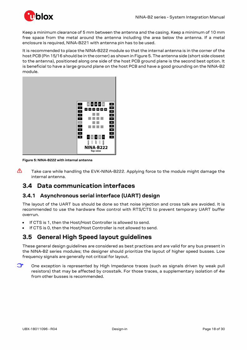
Keep a minimum clearance of 5 mm between the antenna and the casing. Keep a minimum of 10 mm free space from the metal around the antenna including the area below the antenna. If a metal enclosure is required, NINA-B221 with antenna pin has to be used.
It is recommended to place the NINA-B222 module so that the internal antenna is in the corner of the host PCB (Pin 15/16 should be in the corner) as shown in Figure 5. The antenna side (short side closest to the antenna), positioned along one side of the host PCB ground plane is the second best option. It is beneficial to have a large ground plane on the host PCB and have a good grounding on the NINA-B2 module.
Figure 5: NINA-B222 with internal antenna
Take care while handling the EVK-NINA-B222. Applying force to the module might damage the internal antenna.
3.4 Data communication interfaces
3.4.1 Asynchronous serial interface (UART) design
The layout of the UART bus should be done so that noise injection and cross talk are avoided. It is recommended to use the hardware flow control with RTS/CTS to prevent temporary UART buffer overrun.
• If CTS is 1, then the Host/Host Controller is allowed to send. • If CTS is 0, then the Host/Host Controller is not allowed to send.
3.5 General High Speed layout guidelines These general design guidelines are considered as best practices and are valid for any bus present in the NINA-B2 series modules; the designer should prioritize the layout of higher speed busses. Low frequency signals are generally not critical for layout.
One exception is represented by High Impedance traces (such as signals driven by weak pull resistors) that may be affected by crosstalk. For those traces, a supplementary isolation of 4w from other busses is recommended.
NINA-B2 series - System Integration Manual
UBX-18011096 - R04 Design-in Page 19 of 30
3.5.1 General considerations for schematic design and PCB floor-planning
• Verify which signal bus requires termination and add series resistor terminations to the schematics.
• Carefully consider the placement of the module with respect to antenna position and host processor.
• Verify with PCB manufacturer allowable stack-ups and controlled impedance dimensioning. • Verify that the power supply design and power sequence are compliant with the specification of
NINA-B2 series module.
3.5.2 Module placement
• Accessory parts like bypass capacitors should be placed as close as possible to the module to improve filtering capability, prioritizing the placement of the smallest size capacitor close to module pads.
Particular care should be taken not to place components close to the antenna area. The designer should carefully follow the recommendations from the antenna manufacturer about the distance of the antenna vs. other parts of the system. The designer should also maximize the distance of the antenna to Hi-frequency busses like DDRs and related components or consider an optional metal shield to reduce interferences that could be picked up by the antenna thus reducing the module’s sensitivity.
• An optimized module placement allows better RF performance. See Antenna interfaces section for more information on antenna consideration during module placement.
3.5.3 Layout and manufacturing
• Avoid stubs on high speed signals. Even through-hole vias may have an impact on signal quality. • Verify the recommended maximum signal skew for differential pairs and length matching of
buses. • Minimize the routing length; longer traces will degrade signal performance. Ensure that maximum
allowable length for high speed busses is not exceeded. • Ensure that you track your impedance matched traces. Consult with your PCB manufacturer early
in the project for proper stack-up definition. • RF and digital sections should be clearly separated on the board. • Ground splitting is not allowed below the module. • Minimize bus length to reduce potential EMI issues from digital busses. • All traces (including low speed or DC traces) must couple with a reference plane (GND or power);
Hi-speed busses should be referenced to the ground plane. In this case, if the designer needs to change the ground reference, an adequate number of GND vias must be added in the area of transition to provide a low impedance path between the two GND layers for the return current.
• Hi-Speed busses are not allowed to change reference plane. If a reference plane change is unavoidable, some capacitors should be added in the area to provide a low impedance return path through the different reference planes.
• Trace routing should keep a distance greater than 3W from the ground plane routing edge. • Power planes should keep a distance from the PCB edge sufficient to route a ground ring around
the PCB, the ground ring must then be connected to other layers through vias.
3.6 Module footprint and paste mask The mechanical outline of the NINA-B2 series modules can be found in the NINA-B2 series Data Sheet [2] . The proposed land pattern layout reflects the pads layout of the module.
The Non Solder Mask Defined (NSMD) pad type is recommended over the Solder Mask Defined (SMD) pad type, which implements the solder mask opening 50 μm larger per side than the corresponding copper pad.
NINA-B2 series - System Integration Manual
UBX-18011096 - R04 Design-in Page 20 of 30
The suggested paste mask layout for the NINA-B2 series modules is to follow the copper mask layout as described in the NINA-B2 series Data Sheet [2] .
These are recommendations only and not specifications. The exact mask geometries, distances and stencil thicknesses must be adapted to the specific production processes of the customer.
3.7 Thermal guidelines The NINA-B2 series modules have been successfully tested in -40 °C to +85 °C. A good grounding should be observed for temperature relief during high ambient temperature.
3.8 ESD guidelines The immunity of devices integrating NINA-B2 modules to Electro-Static Discharge (ESD) is part of the Electro-Magnetic Compatibility (EMC) conformity, which is required for products bearing the CE marking, compliant with the R&TTE Directive (99/5/EC), the EMC Directive (89/336/EEC) and the Low Voltage Directive (73/23/EEC) issued by the Commission of the European Community.
Compliance with these directives implies conformity to the following European Norms for device ESD immunity: ESD testing standard CENELEC EN 61000-4-2 and the radio equipment standards ETSI EN 301 489-1, ETSI EN 301 489-7, ETSI EN 301 489-24, the requirements of which are summarized in Table 6.
The ESD immunity test is performed at the enclosure port, defined by ETSI EN 301 489-1 as the physical boundary through which the electromagnetic field radiates. If the device implements an integral antenna, the enclosure port is seen as all insulating and conductive surfaces housing the device. If the device implements a removable antenna, the antenna port can be separated from the enclosure port. The antenna port includes the antenna element and its interconnecting cable surfaces.
The applicability of ESD immunity test to the whole device depends on the device classification as defined by ETSI EN 301 489-1. Applicability of ESD immunity test to the related device ports or the related interconnecting cables to auxiliary equipment, depends on the device accessible interfaces and manufacturer requirements, as defined by the ETSI EN 301 489-1.
Contact discharges are performed at conductive surfaces, while air discharges are performed at insulating surfaces. Indirect contact discharges are performed on the measurement setup horizontal and vertical coupling planes as defined in the CENELEC EN 61000-4-2.
For the definition of integral antenna, removable antenna, antenna port, and device classification, refer to the ETSI EN 301 489-1. For the contact and air discharges definitions, refer to CENELEC EN 61000-4-2.
Application Category Immunity Level
All exposed surfaces of the radio equipment and ancillary equipment in a representative configuration
Indirect Contact Discharge ±8 kV
Table 6: Electro-Magnetic Compatibility ESD immunity requirements as defined by CENELEC EN 61000-4-2, ETSI EN 301 489-1, ETSI EN 301 489-7, ETSI EN 301 489-24
NINA-B2 is manufactured taking into account specific standards to minimize the occurrence of ESD events; the highly automated process complies with the IEC61340-5-1 (STM5.2-1999 Class M1 devices) standard. Thus, the designer should implement proper measures to protect from ESD events any pin that may be exposed to the end user.
Compliance with standard protection level specified in the EN61000-4-2 can be achieved by including the ESD protections in parallel to the line, close to areas accessible by the end user.
NINA-B2 series - System Integration Manual
UBX-18011096 - R04 Handling and soldering Page 21 of 30
4 Handling and soldering No natural rubbers, hygroscopic materials or materials containing asbestos are employed.
4.1 Packaging, shipping, storage and moisture preconditioning For information pertaining to reels, tapes or trays, moisture sensitivity levels (MSL), shipment and storage, as well as drying for preconditioning refer to NINA-B2 series Data Sheet [2] and u-blox Package Information Guide [3].
4.2 Handling
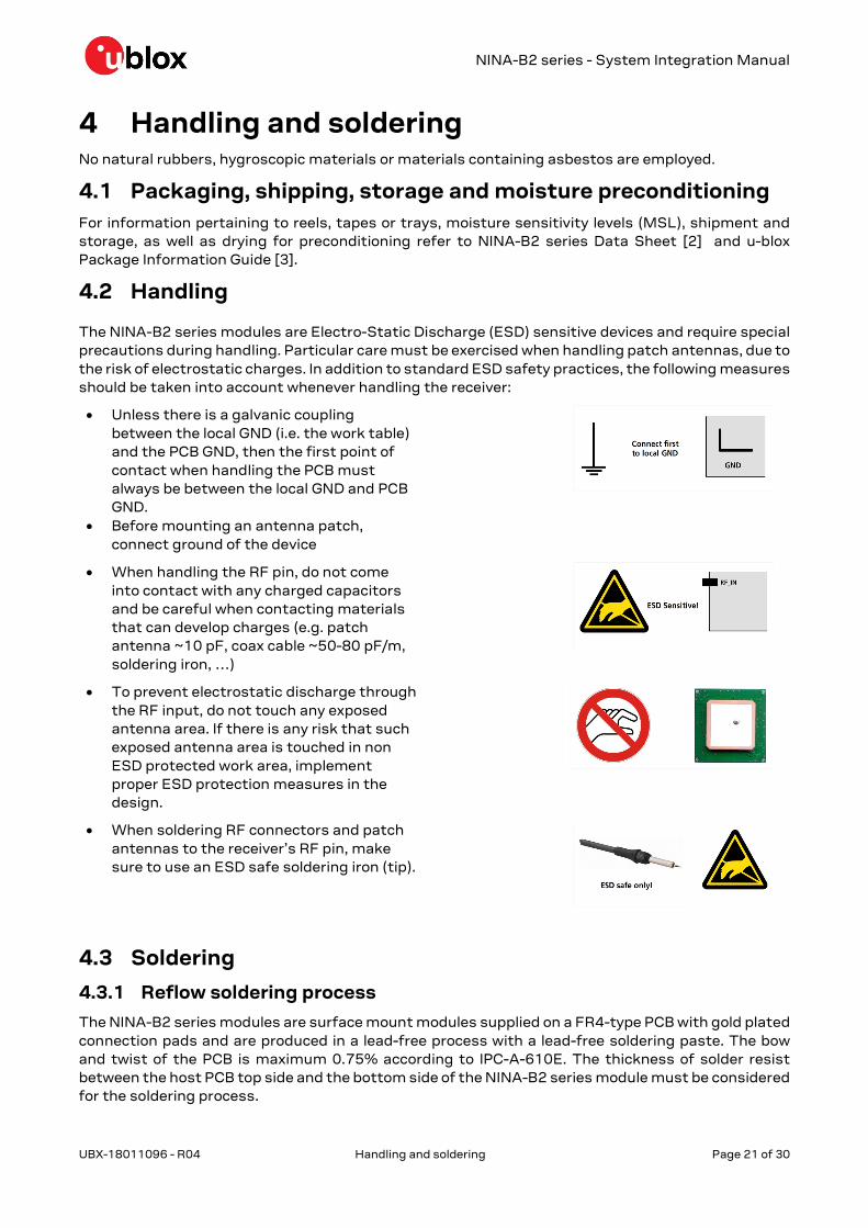
The NINA-B2 series modules are Electro-Static Discharge (ESD) sensitive devices and require special precautions during handling. Particular care must be exercised when handling patch antennas, due to the risk of electrostatic charges. In addition to standard ESD safety practices, the following measures should be taken into account whenever handling the receiver:
• Unless there is a galvanic coupling between the local GND (i.e. the work table) and the PCB GND, then the first point of contact when handling the PCB must always be between the local GND and PCB GND.
• Before mounting an antenna patch, connect ground of the device
• When handling the RF pin, do not come into contact with any charged capacitors and be careful when contacting materials that can develop charges (e.g. patch antenna ~10 pF, coax cable ~50-80 pF/m, soldering iron, …)
• To prevent electrostatic discharge through the RF input, do not touch any exposed antenna area. If there is any risk that such exposed antenna area is touched in non ESD protected work area, implement proper ESD protection measures in the design.
• When soldering RF connectors and patch antennas to the receiver’s RF pin, make sure to use an ESD safe soldering iron (tip).
4.3 Soldering
4.3.1 Reflow soldering process
The NINA-B2 series modules are surface mount modules supplied on a FR4-type PCB with gold plated connection pads and are produced in a lead-free process with a lead-free soldering paste. The bow and twist of the PCB is maximum 0.75% according to IPC-A-610E. The thickness of solder resist between the host PCB top side and the bottom side of the NINA-B2 series module must be considered for the soldering process.
NINA-B2 series - System Integration Manual
UBX-18011096 - R04 Handling and soldering Page 22 of 30
The module is compatible with industrial reflow profile for RoHS solders. Use of "No Clean" soldering paste is strongly recommended.
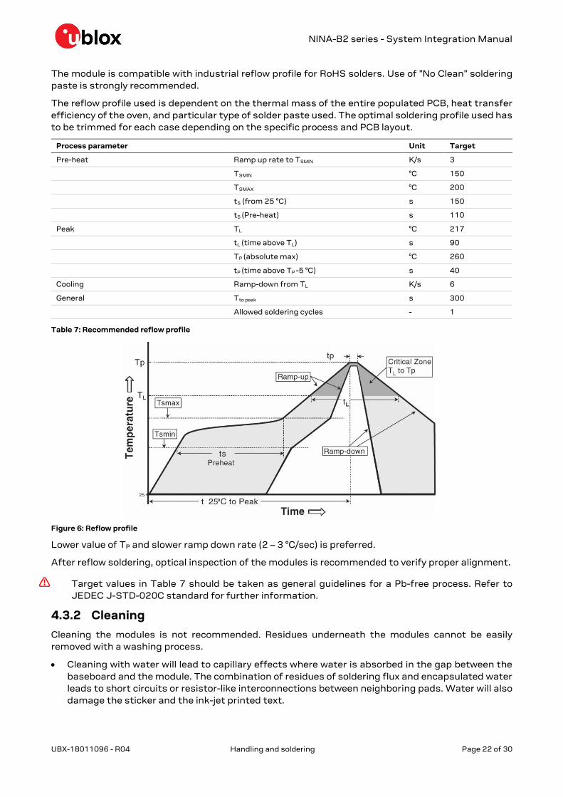
The reflow profile used is dependent on the thermal mass of the entire populated PCB, heat transfer efficiency of the oven, and particular type of solder paste used. The optimal soldering profile used has to be trimmed for each case depending on the specific process and PCB layout.
Process parameter Unit Target
Pre-heat Ramp up rate to TSMIN K/s 3
TSMIN °C 150
TSMAX °C 200
tS (from 25 °C) s 150
tS (Pre-heat) s 110
Peak TL °C 217
tL (time above TL) s 90
TP (absolute max) °C 260
tP (time above TP -5 °C) s 40
Cooling Ramp-down from TL K/s 6
General Tto peak s 300
Allowed soldering cycles - 1
Table 7: Recommended reflow profile
Figure 6: Reflow profile
Lower value of TP and slower ramp down rate (2 – 3 °C/sec) is preferred.
After reflow soldering, optical inspection of the modules is recommended to verify proper alignment.
Target values in Table 7 should be taken as general guidelines for a Pb-free process. Refer to JEDEC J-STD-020C standard for further information.
4.3.2 Cleaning
Cleaning the modules is not recommended. Residues underneath the modules cannot be easily removed with a washing process.
• Cleaning with water will lead to capillary effects where water is absorbed in the gap between the baseboard and the module. The combination of residues of soldering flux and encapsulated water leads to short circuits or resistor-like interconnections between neighboring pads. Water will also damage the sticker and the ink-jet printed text.

NINA-B2 series - System Integration Manual
UBX-18011096 - R04 Handling and soldering Page 23 of 30
• Cleaning with alcohol or other organic solvents can result in soldering flux residues flooding into the two housings, areas that are not accessible for post-wash inspections. The solvent will also damage the sticker and the ink-jet printed text.
• Ultrasonic cleaning will permanently damage the module, in particular the crystal oscillators.
For best results, use a "no clean" soldering paste and eliminate the cleaning step after the soldering process.
4.3.3 Other remarks
• Only a single reflow soldering process is allowed for boards with a module populated on it. • Boards with combined through-hole technology (THT) components and surface-mount
technology (SMT) devices may require wave soldering to solder the THT components. Only a single wave soldering process is allowed for boards populated with the modules. Miniature Wave Selective Solder process is preferred over traditional wave soldering process.
• Hand soldering is not recommended. • Rework is not recommended. • Conformal coating may affect the performance of the module, it is important to prevent the liquid
from flowing into the module. The RF shields do not provide protection for the module from coating liquids with low viscosity, therefore care is required in applying the coating. Conformal coating of the module will void the warranty.
• Grounding metal covers: attempts to improve grounding by soldering ground cables, wick or other forms of metal strips directly onto the EMI covers is done at the customer's own risk and will void module’s warranty. The numerous ground pins are adequate to provide optimal immunity to interferences.
• The module contains components that are sensitive to Ultrasonic Waves. Use of any ultrasonic processes such as cleaning, welding etc., may damage the module. Use of ultrasonic processes on an end product integrating this module will void the warranty.
NINA-B2 series - System Integration Manual
UBX-18011096 - R04 Approvals Page 24 of 30
5 Approvals For additional regulatory information, see the NINA-B2 series Datasheet [2].
5.1 General requirements The NINA-B2 series modules comply with the regulatory demands of Federal Communications Commission (FCC), Industry Canada (IC)2 and the CE mark. This section provides the instructions that must be followed by an integrator while including NINA-B2 series into an end product.
• Any changes to hardware, hosts or co-location configuration may require new radiated emission and SAR evaluation and/or testing.
• The regulatory compliance of NINA-B2 series does not exempt the end product from being evaluated against applicable regulatory demands; for example, FCC Part 15B criteria for unintentional radiators [9].
• Only authorized antenna(s) may be used. • Any notification to the end user about how to install or remove the integrated radio module is NOT
allowed.
5.2 FCC/IC End-product regulatory compliance u-blox warrants that the modular transmitter fulfills the FCC/IC regulations when operating in authorized modes on any host product given that the integrator follows the instructions as described in this document.
5.2.1 NINA-B2 series FCC ID and IC certification number
An end product integrating the NINA-B2 series module using u-blox connectivity software can refer to the u-blox FCC ID and IC certification number.
u-blox can support updates to the u-blox regulatory authorization, if needed. For example, adding new antennas to the u-blox authorization for NINA-B2 module using the antenna pin.
5.2.2 Antenna requirements
In addition to the general requirement to use only authorized antennas, the u-blox grant also requires a separation distance of at least 20 cm from the antenna to all persons. Also, the antenna must not be co-located with any other antenna or transmitter (simultaneous transmission) as well. If this cannot be met, a Permissive Change as described below must be made to the grant.
5.2.2.1 Separation distance
If the required separation distance of 20 cm cannot be fulfilled, a SAR evaluation must be performed. This consists of additional calculations and/or measurements. The result must be added to the grant file as a Class II Permissive Change.
5.2.2.2 Co-location (simultaneous transmission)
If the module is to be co-located with another transmitter, additional measurements for simultaneous transmission is required. The results must be added to the grant file as a Class II Permissive Change.
5.2.2.3 Adding a new antenna for authorization
If the authorized antennas and/or antenna trace design cannot be used, the new antenna and/or antenna trace designs must be added to the grant file. This is done by a Class I Permissive Change or a Class II Permissive Change, depending on the specific antenna and antenna trace design.
• Antennas of the same type and with less or same gain as an already approved antenna can be added under a Class I Permissive Change.
2 Official name is Innovation, Science and Economic Development (ISED) Canada.
NINA-B2 series - System Integration Manual
UBX-18011096 - R04 Approvals Page 25 of 30
• Antenna trace designs deviating from the u-blox reference design and new antenna types are added under a Class II Permissive Change.
Integrators who want to refer to the u-blox FCC ID / IC certification ID must send an email to the support team email address for your area as listed in the Contact section to discuss the Permissive Change Process. Class II Permissive Changes will be subject to NRE costs.

NINA-B2 series - System Integration Manual
UBX-18011096 - R04 Product testing Page 26 of 30
6 Product testing 6.1 u-blox In-Series production test u-blox focuses on high quality for its products. All units produced are fully tested automatically in production line. Stringent quality control process has been implemented in the production line. Defective units are analyzed in detail to improve the production quality.
This is achieved with automatic test equipment (ATE) in production line, which logs all production and measurement data. A detailed test report for each unit can be generated from the system. Figure 7 illustrates typical automatic test equipment (ATE) in a production line.
The following tests are performed as part of the production tests:
• Digital self-test (firmware download, MAC address programming) • Measurement of currents • Functional tests • Digital I/O tests • Measurement and verification of RF characteristics in all supported bands (calibration of
transmitter power levels, modulation and frequency accuracy, power levels, sensitivity, and so on.)
Figure 7: Automatic test equipment for module test
6.2 OEM manufacturer production test As the testing is already done by u-blox, an OEM manufacturer does not need to repeat firmware tests or measurement of the module’s RF performance or tests over analog and digital interfaces in their production test.
However, an OEM manufacturer should focus on:
• Module assembly on the device: It should be verified that: o Soldering and handling process did not damage the module components o All module pins are well soldered on device board o There are no short circuits between the pins
• Component assembly on the device: It should be verified that: o Communication with the host controller can be established o The interfaces between the module and device are working o Overall RF performance test of the device including antenna
NINA-B2 series - System Integration Manual
UBX-18011096 - R04 Product testing Page 27 of 30
Dedicated tests can be implemented to check the device. For example, the measurement of module current consumption when set in a specified state can detect a short circuit if compared with a “Golden Device” result.
The standard operational module firmware and test software on the host can be used to perform functional tests (communication with the host controller, check interfaces) and to perform basic RF performance tests.
6.2.1 “Go/No go” tests for integrated devices
A “Go/No go” test compares the signal quality with a “Golden Device” in a location with known signal quality. This test can be performed after establishing a connection with an external device.
A very simple test can be performed by just scanning for a known Bluetooth low energy device and checking the signal level.
These kinds of test may be useful as a “go/no go” test but not for RF performance measurements.
This test is suitable to check the functionality of the communication with the host controller and the power supply. It is also a means to verify if the components are well soldered.
A basic RF functional test of the device including the antenna can be performed with standard Bluetooth low energy devices as remote stations. The device containing the NINA-B2 series module and the antennas should be arranged in a fixed position inside an RF shield box to prevent interferences from other possible radio devices to get stable test results.
NINA-B2 series - System Integration Manual
UBX-18011096 - R04 Appendix Page 28 of 30
Appendix
A Glossary Abbreviation Definition
AP Access Point
ATE Automatic Test Equipment
BP Band Pass
BPF Band Pass Filter
BT Bluetooth
CAN Controller Area Network
CPU Central Processing Unit
CTS Clear To Send
DC Direct Current
DDR Double Data Rate
DSR Data Set Ready
DTR Data Terminal Ready
EIRP Equivalent Isotropically Radiated Power
EMC Electro-magnetic Compatibility
EMI Electromagnetic Interference
ESD Electro-Static Discharge
GND Ground
IoT Internet of Things
ISM Industrial, Scientific, and Medical radio
LED Light-Emitting Diode
LTE Long-Term Evolution
MAC Media Access Control
MCU Microcontroller
MCS Modulation Coding Scheme
MSL Moisture Sensitivity Level
NSMD Non Solder Mask Defined
OEM Original Equipment Manufacturer
PCB Printed Circuit Board
RF Radio Frequency
ROM Read-only Memory
RMII Reduced Media-independent Interface
RSSI Received Signal Strength Indicator
SMA SubMiniature version A
SRAM Static random-access memory
THT Through-hole Technology
UART Universal Asynchronous Receiver-Transmitter
Table 8: Explanation of abbreviations used
NINA-B2 series - System Integration Manual
UBX-18011096 - R04 Related documents Page 29 of 30
Related documents [1] u-blox Short Range AT Commands Manual, document number UBX-14044127 [2] NINA-B2 Series DataSheet, document number UBX-18006649 [3] u-blox Package Information Guide, document number UBX-14001652 [4] NINA-B2 Getting Started, document number UBX-18020603
For regular updates to u-blox documentation and to receive product change notifications, register on our homepage (www.u-blox.com).
Revision history Revision Date Name Comments
R01 27-Apr-2018 fbro, kgom Initial release.
R02 3-Jul-2018 cmag, kgom Modified the product status to Engineering Sample on page 2. Provided reference to NINA-B2 Getting Started.
R03 28-Jan-2019 fbro, mwej Modified the product status to Initial Production. Removed support for external LPO clock (section 1.4.1). Updated block diagram (Figure 1). Updated Output power data (Table 1). Removed pending status for FCC/IC approval in section 5.
R04 17-Dec-2019 flun Cleaned up Applicable Products section.
NINA-B2 series - System Integration Manual
UBX-18011096 - R04 Contact Page 30 of 30
Contact For complete contact information, visit us at www.u-blox.com.
u-blox Offices
North, Central and South America
u-blox America, Inc.
Phone: +1 703 483 3180 E-mail: [email protected]
Regional Office West Coast:
Phone: +1 408 573 3640 E-mail: [email protected]
Technical Support:
Phone: +1 703 483 3185 E-mail: [email protected]
Headquarters Europe, Middle East, Africa
u-blox AG
Phone: +41 44 722 74 44 E-mail: [email protected] Support: [email protected]
Asia, Australia, Pacific
u-blox Singapore Pte. Ltd.
Phone: +65 6734 3811 E-mail: [email protected] Support: [email protected]
Regional Office Australia:
Phone: +61 2 8448 2016 E-mail: [email protected] Support: [email protected]
Regional Office China (Beijing):
Phone: +86 10 68 133 545 E-mail: [email protected] Support: [email protected]
Regional Office China (Chongqing):
Phone: +86 23 6815 1588 E-mail: [email protected] Support: [email protected]
Regional Office China (Shanghai):
Phone: +86 21 6090 4832 E-mail: [email protected] Support: [email protected]
Regional Office China (Shenzhen):
Phone: +86 755 8627 1083 E-mail: [email protected] Support: [email protected]
Regional Office India:
Phone: +91 80 405 092 00 E-mail: [email protected] Support: [email protected]
Regional Office Japan (Osaka):
Phone: +81 6 6941 3660 E-mail: [email protected] Support: [email protected]
Regional Office Japan (Tokyo):
Phone: +81 3 5775 3850 E-mail: [email protected] Support: [email protected]
Regional Office Korea:
Phone: +82 2 542 0861 E-mail: [email protected] Support: [email protected]
Regional Office Taiwan:
Phone: +886 2 2657 1090 E-mail: [email protected] Support: [email protected]


