
NanoscienceNanoscience & & MicroscopiesMicroscopiesOptical MicroscopeOptical MicroscopeSEM, AFM & STMSEM, AFM & STM

Simple Optical MicroscopeSimple Optical MicroscopeSimple Optical Microscope
://www.substech.com/dokuwiki/lib/exe/fetch.php
A few more lenses than we used in class !

Confocal MicroscopeConfocalConfocal MicroscopeMicroscope
http://www.microscopyu.com/articles/confocal/confocalintrobasics.html
Used in medicine & medical research

Through a MicroscopeThrough a Microscope
www.answers.com/topic/microscopy
Sea urchin (left) & Pollen (below)

More Optical MicroscopyMore Optical Microscopy
Bugs & Vitamin C (color enhanced)

Block Diagram of EBlock Diagram of E--beambeam

SEM SEM PictsPicts

Ostrinium Nubilialis
Dendritic Growth
SEM SEM PictsPicts

Miami ResearchMiami ResearchResultsResults

Nanowires & NanosheetsNanowiresNanowires & & NanosheetsNanosheets

STM BasicsSTM BasicsSTM Basics

STM -=- Nobel Prize Material!STM STM --==-- Nobel Prize Material!Nobel Prize Material!
http://nobelprize.org/physics/educational/microscopes/scanning/
1981 Invention by two scientists from IBM Zurich
Gerd Binning & Heinrich Rohrer
1986Nobel Prize awarded !!
Only 5 years later -- a record !
1981 Invention by two scientists from IBM Zurich
Gerd Binning & Heinrich Rohrer
1986Nobel Prize awarded !!
Only 5 years later -- a record !

Two Principles…Two PrinciplesTwo Principles……Quantum Tunneling for “seeing” surfaces
Piezo-electric Effect for scanning surfaces
Quantum Tunneling for “seeing” surfaces
Piezo-electric Effect for scanning surfaces
This is the STM image of Si(111)-7x7 surface, the white spots represents the position of the atoms.

Electron Wave BehaviorOutside the Barrier
Electron Wave BehaviorElectron Wave BehaviorOutside the BarrierOutside the Barrier
Wavefunction extends outside of STM tip

At close approach,Electron Waves can Breach the
Air!
At close approach,Electron Waves can Breach the
Air!
Electrons can tunnel through the air from tip to sample depending on…
Electrons can tunnel through the air from tip to sample depending on…
http://phys.educ.ksu.edu/vqm/html/qtunneling.html
Barrier separationElectron energy
Barrier separationElectron energy

Introducing the STM…Introducing the STM…
http://www.iap.tuwien.ac.at/www/surface/STM_Gallery/stm_schematic.html

Closer look…Closer look…
www.nano.geo.uni-muenchen.de/stm

STM Tip in detail…STM Tip in detail…
www.chem.ucla.edu/~kodohert/0f1b3060

Scanning the STM tip…Scanning the STM tip…
www.surfaces.lsu.edu/STMoverview.html

Modes of OperationModes of OperationConstant Current
Constant Height
Constant Current
Constant Height
userpage.chemie.fu-berlin.de/.../html/node5.htm

Important note:Important note:Important note:Remember, the STM works because of electron tunneling between the surface of interest and the scanning tip.Thus--> Nuclear position is NOT probedTHEREFORE --> we are probing what?
Remember, the STM works because of electron tunneling between the surface of interest and the scanning tip.Thus--> Nuclear position is NOT probedTHEREFORE --> we are probing what?

Use of STMUse of STMExcitation of different vibrationalmodes depending on species (C2H2vs. C2D2)
Science, 280, 1715 (1998).
Single molecule chemical reactionsScience News, 158, 215 (2000).
Excitation of different vibrationalmodes depending on species (C2H2vs. C2D2)
Science, 280, 1715 (1998).
Single molecule chemical reactionsScience News, 158, 215 (2000).

This is the STM image of Si(111)-7x7 surface, the white spots represents the position of the atoms.
This is the STM image of Si(111)-7x7 surface, the white spots represents the position of the atoms.
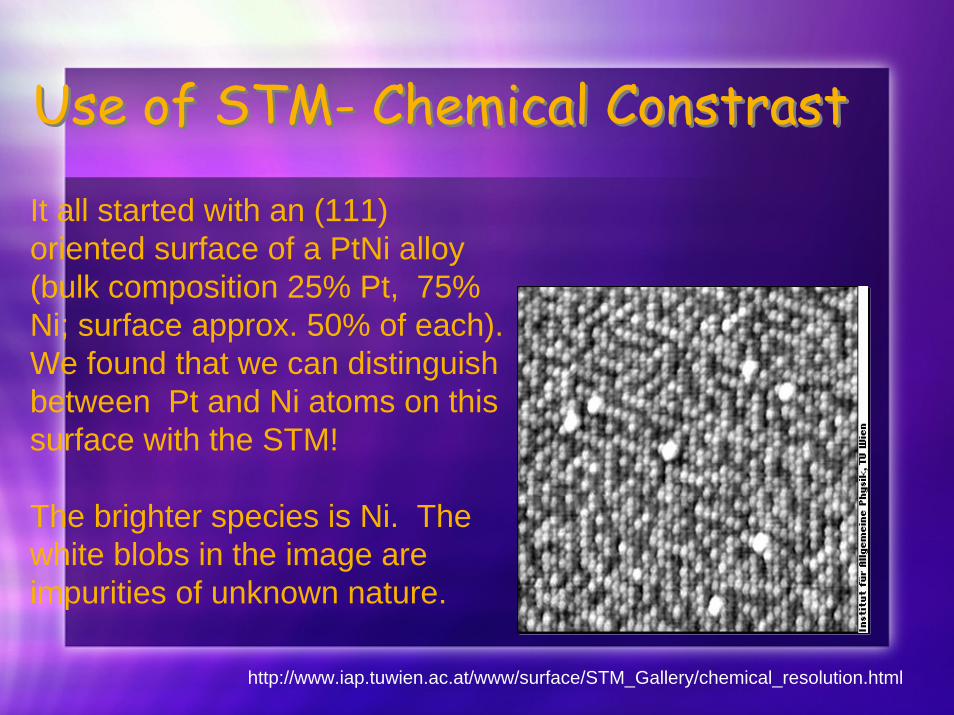
Use of STM- Chemical ConstrastUse of STM- Chemical Constrast
http://www.iap.tuwien.ac.at/www/surface/STM_Gallery/chemical_resolution.html
It all started with an (111) oriented surface of a PtNi alloy (bulk composition 25% Pt, 75% Ni; surface approx. 50% of each). We found that we can distinguish between Pt and Ni atoms on this surface with the STM!
The brighter species is Ni. The white blobs in the image are impurities of unknown nature.

Phys. Rev. Lett. 94, 046101
Researchers usually compare "before" and "after" pictures of typical regions of a material to see how it changes during a phase transition. This is now see on an atomic scale.
As the lead atoms in this 20 x 13 nanometer region are warmed from 40 to 136 Kelvin, they switch from the corrugated to the flat arrangement at the transition temperature of 86 Kelvin .Vienna University of Technology

Downside to STM?Downside to STM?Requires electrical path – for tunneling
Gives information of heights of electron clouds above surface – eg. graphite structure
Some questions cannot be explored
Requires electrical path – for tunneling
Gives information of heights of electron clouds above surface – eg. graphite structure
Some questions cannot be explored

Other cool sites…Other cool sites…http://www.almaden.ibm.com/vis/stm(Interesting STM images)
http://www.nobel.se/physics/educational/microscopes/scanning/ (Interesting STM images)
http://www.nanoscience.com/education/gallery/DDB.mpg (movie of scanned image)
http://www.almaden.ibm.com/vis/stm(Interesting STM images)
http://www.nobel.se/physics/educational/microscopes/scanning/ (Interesting STM images)
http://www.nanoscience.com/education/gallery/DDB.mpg (movie of scanned image)

Atomic Force MicroscopyAtomic Force Microscopy
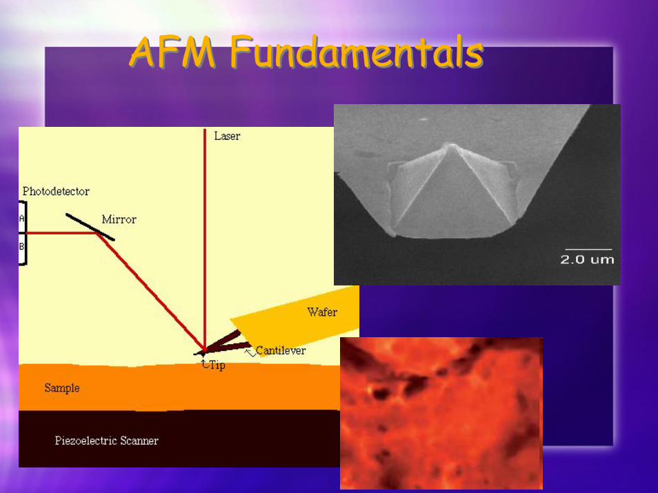
AFM FundamentalsAFM Fundamentals

AFMAFMThe AFM or Atomic Force Microscope was developed in 1986 – soon after the STM
The AFM was an offshoot of the STM which was limited to samples which were conducting in order to scan them
The AFM can operate in contact mode or non-contact mode
The AFM or Atomic Force Microscope was developed in 1986 – soon after the STM
The AFM was an offshoot of the STM which was limited to samples which were conducting in order to scan them
The AFM can operate in contact mode or non-contact mode

THE AFM TIPTHE AFM TIPThe AFM tip is generally made of silicon or silicon nitride
The tip is usually pyramidal or conical in shape with a ~10 nm end (~100 atoms)
The tip must be durable, and sharp enough to see surface features
The AFM tip is generally made of silicon or silicon nitride
The tip is usually pyramidal or conical in shape with a ~10 nm end (~100 atoms)
The tip must be durable, and sharp enough to see surface features
http://www.weizmann.ac.il/Chemical_Research_Support/surflab/peter/afmworks/

AFM Tip & CantileverAFM Tip & Cantilever
http://www.mobot.org/jwcross/spm/
The AFM tip is attached to a cantilever ~10 microns long
The cantilever must be flexible to allow for the scanning across various surface heights
http://en.wikipedia.org/wiki/Atomic_force_microscope

Wafer & TIPWafer & TIPSi or SiN – 10 nm at end – ~100 atomsSi or SiN – 10 nm at end – ~100 atoms
http://stm2.nrl.navy.mil/how-afm/how-afm.html
Electron micrograph of two 100 µm long V-shaped cantilevers (by Jean-Paul Revel, Caltech; cantilevers from Park Scientific Instruments, Sunnyvale, CA).
Three common types of AFM tip. (a) normal tip (3 µm tall); (b) supertip; (c) Ultralever (also 3 µm tall). (b) Electron micrographs by Jean-Paul Revel, Caltech.

Resolution of ALL Scanning ProbesResolution of ALL Scanning ProbesTip shape AND surface shape are convolved into shape recorded by probes.
Tip shape AND surface shape are convolved into shape recorded by probes.

Height & the AFMHeight & the AFMWhen tip is close to surface,Hooke’s Law takes over Hooke’s Law?F = k xForces between surface and tip deflect the cantilever
When tip is close to surface,Hooke’s Law takes over Hooke’s Law?F = k xForces between surface and tip deflect the cantilever
http://en.wikipedia.org/wiki/Atomic_force_microscope

Feedback & ScanningFeedback & ScanningPiezos –Again !Piezos –Again !
http://veecolifesciences.com/AFM_Basics.aspx

Why Feedback?Why Feedback?
Used AFM tip
Used AFM tip

AFMAFMScans microns of areaCan be in contact mode if surface is strongCan be in non-contact mode if have objects on surface to scanCan also use tapping mode
Scans microns of areaCan be in contact mode if surface is strongCan be in non-contact mode if have objects on surface to scanCan also use tapping mode

AFM ModesAFM ModesContact
Low and High GainLow gain – “drag” tip across sample see deflection which is OK for relatively flat surfacesHigh gain – tries to push down on sample to maintain a particular height which is OK for more bumpy surfaces, but not for soft surfaces
- Tapping modeGood for local surface distortions to measure friction and spring forces on surfaces
Non-contactRequires a frequency modulation technique which is good for biological samples- repulsive forces from surface
Contact Low and High Gain
Low gain – “drag” tip across sample see deflection which is OK for relatively flat surfacesHigh gain – tries to push down on sample to maintain a particular height which is OK for more bumpy surfaces, but not for soft surfaces
- Tapping modeGood for local surface distortions to measure friction and spring forces on surfaces
Non-contactRequires a frequency modulation technique which is good for biological samples- repulsive forces from surface

Metrology -- FabricationMetrology -- FabricationAFM can be used to study the success of e-beam lithography and subsequent processing steps.
AFM can be used to study the success of e-beam lithography and subsequent processing steps.
Nanotechnology, 13 659 (2002).


Tobacco Mosaic VirusTobacco Mosaic Virus

Non-Contact Mode – SolidLipid NanoparticlesNon-Contact Mode – SolidLipid Nanoparticles

Which probe microscope do I use?Which probe microscope do I use?
Optical Microscope – good for objects in the 1-100 micron range (10-6m)SEM – provides range from microns to 10 nmAFM – microns of scan range, 10s of nm resolution, tip 10nmSTM – nm of scan range, angstrom resolution, tip single atom
Optical Microscope – good for objects in the 1-100 micron range (10-6m)SEM – provides range from microns to 10 nmAFM – microns of scan range, 10s of nm resolution, tip 10nmSTM – nm of scan range, angstrom resolution, tip single atom


