NANOCOMPOSITES: CHARACTERIZATION AND APPLICATIONS
TOWARDS ELECTRICAL ENERGY STORAGE DEVICES
_______________________________
A Dissertation
presented to the Faculty of the Graduate School
at the University of Missouri
________________________________________________
In Partial Fulfillment
of the Requirements for the Degree
Doctor of Philosophy
________________________________________________
by
STEVEN C. HAMM
Dr. Shubhra Gangopadhyay, Dissertation Supervisor
June 2014
The undersigned, appointed by the Dean of the Graduate School, have examined the dissertation entitled
NANOCOMPOSITES: CHARACTERIZATION AND APPLICATIONS TOWARDS ENERGY STORAGE DEVICES
presented by Steven Hamm
a candidate for the degree of Doctor of Philosophy in Electrical and Computer Engineering
and hereby certify that, in their opinion, it is worthy of acceptance.
Professor Shubhra Gangopadhyay
Professor Scott Kovaleski
Professor John Gahl
Professor Gary Baker
Adjunct Faculty Member Luke Currano

ii
Acknowledgments
First and foremost, I would like to thank Dr. Shubhra Gangopadhyay for her
support, intellectual insight, and drive to help push me to become a better researcher. The
experience and knowledge I have gained from the large variety of projects obtained under
her supervision is more than I could have ever hoped for in pursuing a graduate degree.
The entire Gangopahdyay Research Group has always been a joy to work with and learn
from. I am extremely lucky to have been given the opportunity to work in her group. I
would also like to thank Dr. Keshab Gangopadhyay, for providing me with additional
research opportunities and support as an intern in his company.
Additional thanks go to the members of my doctoral committee. Dr. John Gahl,
Dr. Scott Kovaleski, Dr. Gary Baker, and Dr. Luke Currano have provided insightful
advice on my research and dissertation. As an undergraduate struggling to find my goal
and purpose as an engineer, it was Dr. Scott Kovaleski who guided me to look into the
realm of research. Without this simple suggestion I probably would not be where I am
today. Dr. Gary Baker has been a strong influence throughout my work, and has helped to
push my publication record and research to new heights. Dr. Luke Currano was gracious
enough to hire me as a summer intern at the Army Research Laboratory in Adelphi, MD.
The work accomplished over this period led to additional research opportunities and
continued on to be a major component within my dissertation.
There are a number of other “little” things for which I will be forever grateful. I
was lucky enough to have superb teachers throughout my life. I would specifically like to
mention Mr. and Mrs. Cloud, who taught high school physics and fifth grade,
respectively. The dedication and energy these teachers exhausted towards ensuring
iii
students learned will never be forgotten, and will always be appreciated. I wish everyone
could experience having such great teachers. Additionally, although there were a number
of factors that led me to pursue a PhD, it was the discussions with Brian Samuels from
the Lafferre machine shop that shined light on the fact that I would most likely regret it if
I didn’t. Without this down-to-earth, no-nonsense insight, who knows where I would be.
Of course, I would also like to thank my family. The insurmountable guidance
and support has been very been a huge influence throughout my life. They are the best.
Last, and most important, I would like to thank my wife. Her love and support has
made this journey much more enjoyable.
The funding for the projects discussed in this dissertation has been provided by
many sources. The Kansas City Plant provided the initial funding for some preliminary
experiments prior to the work discussed in Chapter 2, under contract number
DE-AC04-01AL66850. Although none of the work is shown in the dissertation, the initial
idea and some preliminary experiments which led to the multilayer capacitor work in
Chapter 3 came from the Army Research Laboratory – Adelphi during my summer
internship. This project was then further funded by the Office of Naval Research (ONR),
under contract number N00014-11-C-0392. Lastly, the work discussed in Chapter 4 and
Chapter 5 was funded by the U.S. Army under contract number
W15QKN-11-9-0001-RPP1.

iv
Page Intentionally Left Blank
v
Table of Contents
Acknowledgments............................................................................................................... ii
List of Figures .................................................................................................................. viii
List of Tables ..................................................................................................................... xi
Abstract ............................................................................................................................. xii
Chapter 1 – Introduction ..................................................................................................... 1
1.1 Capacitor Basics ........................................................................................................ 2
1.2 Nanocomposites within Capacitors ........................................................................... 5
1.2.1 Dielectric Capacitors .......................................................................................... 5
1.2.2 Electrochemical Double Layer Capacitors ......................................................... 8
1.3 Scope of the Dissertation ........................................................................................ 13
1.4 References ............................................................................................................... 15
Chapter 2 – Characterization of SiOCN Grown by PECVD towards use in Thin Film Capacitors ......................................................................................................................... 18
2.1 Introduction ............................................................................................................. 18
2.2 Materials and Methods ............................................................................................ 20
2.3 Results and Discussion ............................................................................................ 23
2.4 Conclusions ............................................................................................................. 45
2.5 References ............................................................................................................... 46
Chapter 3 – Thin Film Multi-layer Capacitors by Highly Selective Etching Techniques 53
3.1 Introduction ............................................................................................................. 53
3.2 Materials and Methods ............................................................................................ 55
3.3 Fabrication Procedure ............................................................................................. 57
3.4 Results and Discussion ............................................................................................ 64
3.5 Conclusions ............................................................................................................. 69
3.6 References ............................................................................................................... 70
Chapter 4 – Investigations into the Crystal Growth of Nanoparticles Sputter-Deposited into Ionic Liquids .............................................................................................................. 72
4.1 Introduction ............................................................................................................. 72
4.2 Materials and Methods ............................................................................................ 74
vi
4.3 Results And Discussion ........................................................................................... 77
4.4 Conclusion ............................................................................................................... 93
4.5 References ............................................................................................................... 95
Chapter 5 – Electrochemical Enhancement of Nanoparticle-in-ionic liquid based electrolytes for Supercapacitor Applications .................................................................... 99
5.1 Introduction ............................................................................................................. 99
5.2 Materials and Methods .......................................................................................... 100
5.3 Results and Discussion .......................................................................................... 103
5.3.1 Potential Windows .......................................................................................... 103
5.3.2 Double-layer Capacitance ............................................................................... 105
5.3.3 Ionic Conductivity .......................................................................................... 109
5.3.4 Electrochemical Impedance Spectroscopy ..................................................... 114
5.4 Conclusion ............................................................................................................. 121
5.5 References ............................................................................................................. 122
Chapter 6 – Conclusions and Future Work ..................................................................... 128
6.1 Conclusions ........................................................................................................... 128
6.1.1 Multilayer Capactitor ...................................................................................... 128
6.1.2 Nanoparticle-in-Ionic Liquid .......................................................................... 128
6.2 Future Direction .................................................................................................... 129
6.2.1 Multilayer Capactitor ...................................................................................... 129
6.2.2 Nanoparticle-in-Ionic Liquid .......................................................................... 131
Appendix A – Further Characterization and Applications of SiOCN ............................ 133
Additional Characterization Methods ......................................................................... 133
Additional Characterization Results ........................................................................... 136
Applications ................................................................................................................ 140
Abrasion Resistant Coating ..................................................................................... 141
Coating on Flexibile Substrates ............................................................................... 142
Direct Charge Nuclear Capacitor ............................................................................ 144
Multi-layer dielectrics .............................................................................................. 149
References ................................................................................................................... 151
Appendix B. EIS fitting results ....................................................................................... 154

vii
Vita .................................................................................................................................. 156
viii
List of Figures
Figure 1-1(a) Illustration of a parallel plate capacitor, and (b) demonstration of how the dipoles within a material placed between two charged plates polarize with the electric field. .................................................................................................................................... 2
Figure 1-2. (a) A simplified illustration demonstrating the charge separation and storage within an EDLC, and (b) photograph of SWCNT electrode deposited by electrophoretic deposition for an EDLC with and an example of an SEM image of the SWCNTs. ......... 10
Figure 2-1. EDS calculated atomic concentrations for a) Si, b) O, c) C, and d) N. Error bars represent the standard deviation. ............................................................................... 25
Figure 2-2. FTIR spectra of SiOCN films growth with (a) silane and (b) TMS precursors at various deposition temperatures. ................................................................................... 27
Figure 2-3. Resolved FTIR absorption coefficient spectra ranges for (left) silane- and (right) TMS-based SiOCN films. ...................................................................................... 31
Figure 2-4. Three-dimensional 500 nm × 500 nm AFM topography images (and 2D inset) of films prepared with (a) silane at 100 °C [ra = 0.58 ± 0.01 nm], (b) silane at 250 °C [0.69 ± 0.09 nm], (c) silane at 400 °C [0.53 ± 0.01 nm], (d) TMS at 100 °C [0.32 ± 0.01 nm], (e) TMS at 250 °C [0.15 ± 0.01 nm], and (f) TMS at 400 °C [0.15 ± 0.01 nm]. The Z-axes are normalized for better visualization of the roughness comparison. .......... 34
Figure 2-5. Low field (<0.1 MV cm-1) resistivity versus deposition temperature measured for ~50 nm and ~1000 nm thick samples. (Inset) Current density vs. electric field measurements for TMS ~1000 nm deposited at various deposition temperatures with best linear fits represented by the lines and corresponding slope values (conductivities). ...... 36
Figure 2-6. Examples of the typical current density versus electric field measurements for ~100 nm thick (a) Silane- and (b) TMS-based films deposited at 100 °C, 250 °C, and 400 °C. .............................................................................................................................. 38
Figure 2-7. Breakdown strength versus thickness for (a) silane and (b) TMS based samples .............................................................................................................................. 40
Figure 2-8. Measured stress of the ~1000 nm thick films versus deposition temperature 41
Figure 2-9. Measured stress and the residual stress calculated by subtracting the theoretical thermal stress developed between Si and SiO2 or SiC. ................................... 43
Figure 3-1. Demonstration of how integrating capacitors into circuit boards will result in decreased board size. ........................................................................................................ 53
Figure 3-2. Thin film multi-layer capacitor fabrication process for a two-layer device. A short description of the process as is follows: (a) deposit all layers alternating Pt and Ru electrodes until desired number of layers is achieved and pattern devices with Cr hard mask, (b) dry etch to define device area, (c) remove Cr mask, expose one side of devices using photolithography and selectively etch Ru, (d) deposit Cr sidewall to connect all exposed Ru electrodes, (e) expose opposite side using photolithography and selectively undercut Pt, (f) deposit another Cr sidewall to connect all exposed Pt electrodes to
ix
complete the devices. An elaborated process description is provided in the text. Illustration not drawn to scale. .......................................................................................... 58
Figure 3-3. Optical microscopy image of the device showing (a) before and (b) after a Ru undercut etching. ............................................................................................................... 62
Figure 3-4. (a) Illustration demonstrating the dimensions of the devices and Cr sidewall electrode pads with units in mm, (b) photograph of six completed devices, and (c) cross-sectional SEM image of completed one-layer device with 1 μm thick dielectric layers showing the Pt layer undercut and connection between the Ru layer and the Cr sidewall............................................................................................................................................ 65
Figure 3-5. (a) Averages and standard deviations of capacitances and dissipation factors measured at 10 kHz versus number of layers for 1 μm thick dielectric devices, and (b) average capacitance versus frequency for one-, two-, and three-layer devices (standard deviation of <6 pF for all data points). ............................................................................. 66
Figure 3-6. Best obtained current leakage measurements for (a) one-, two-, and three-layer devices with 1 μm thick dielectric layers, and (b) one-layer devices with 3.5 μm thick dielectric layers. Inset: Current density versus electric field, calculated from the area of the device (2.5 mm × 2.5 mm) and the corresponding dielectric thickness. ................ 68
Figure 4-1. IL spread on a Si wafer (a) before and (b) after Au deposition ..................... 76
Figure 4-2. (a) raw UV–Vis spectra of diluted [emim][EtSO4] with AuNPs at various times after deposition, (b) SPR peak growth with time, (c) peak wavelength position, and (d) peak absorbance values over time (data in (c) and (d) are taken from marked points in (b)). Results are normalized to the wt% of the first measurement. ................................... 80
Figure 4-3. HRTEM images of AuNPs in [emim][EtSO4] (a) 0.5 h, (b) 7.5 h, (c) 43.3 h after deposition with corresponding size histogram and mean particle sizes of 1.3 ± 0.7 nm, 3.0 ± 1.2, and 4.9 ± 2.9 nm, respectively. (d) Peak absorbance and particle size measured versus time after deposition. ............................................................................. 82
Figure 4-4. HRTEM images of (a) a 3.4 nm particle 7.5 h after deposition and (b) a 5.7 nm particle 43.3 h after deposition with the corresponding fast Fourier transform (FFT) pattern obtained from ImageJ software provide in the inset. The FFT pattern represent an FCC crystal along the <110> zone axis. ........................................................................... 84
Figure 4-5. TEM images of (a) [hmim][BF4] Au50, (b) [emim][Tf2N] Ag340 with higher magnification supplied in the inset, and (c) [hmim][PF6] Ag340. .................................... 85
Figure 4-6. Photograph of [P14,666][Cl] after ~90 nm Au deposition showing no color change and (inset) resulting UV-Vis showing no SPR peak indicating Au particles (if present) remain <1 nm. ..................................................................................................... 87
Figure 4-7. Schematic showing proposed nanoparticle growth mechanism depending on interaction energy between metal and ions. (A) The sputtered material first enters the ionic liquid as atoms which (B) start to come together as single crystals, and depending on the interaction energy between the ions and the metal form (i) remain small (<1 nm) crystals for sufficiently high interaction energy, (ii) single crystal nanoparticles for intermediate interaction energy, and (iii) polycrystalline nanoparticles due to low interaction energy.............................................................................................................. 89
x
Figure 4-8. UV–Vis absorbance spectra of Au in [emim][EtSO4] comparing the effects of storage at room temperature and at -5 °C. ........................................................................ 91
Figure 4-9. (a) Change in SPR absorbance as a function of time for the sample left at room temperature following Au deposition and a sample stored at +5 °C for 27 days prior to storing at RT. (b) the change in absorbance as a function of time where 0 h is the time placed at RT. ..................................................................................................................... 93
Figure 5-1. CV measurements taken (a) immediately following Ag deposition into [hmim][PF6], (b) after 34 days after deposition, and (c) calculated CV voltage windows over time after deposition. Dashed lines are provided to guide the eye only. Black line represents the control value. ........................................................................................... 104
Figure 5-2. CV measurements taken (a) 1 h, (b) 2 h, (c) 8 h, and (d) 20 h after Au deposition ........................................................................................................................ 106
Figure 5-3. (a) Calculated double-layer capacitance from CV measurements calculated by averaging the currents obtained from the final three scans and (b) mean difference in forward and reverse sweeping currents with respect to time after deposition. The dashed lines are provided to guide the eye only. ........................................................................ 108
Figure 5-4. Examples of ionic conductivity versus time after deposition for (a) [omim][BF4] and (b) [Bmpy][Tf2N]. Dashed lines are provided to guide the eye only. Black line represents the control value. .......................................................................... 110
Figure 5-5. Waldon plot of the investigated ILs with Au or Ag NPs ............................. 111
Figure 5-6. (a) Randles circuit, (b) cartoon representation of the cross-sectional view of the electrochemical test cell, and (c) the circuit model used for fitting the experimental EIS data. .......................................................................................................................... 115
Figure 5-7. Nyquist plots (a) 0.3 h, (b) 2 h, (c) 7.5 h, and (d) 20 h after Au deposition. Symbols are experimental results, and lines represent best fit. ...................................... 117
Figure 5-8. Ratio between the (a) electrolyte resistances and (b) double layer CPE coefficients with AuNP with respect to neat [emim][EtSO4]. The dashed lines are provided to guide the eye only. ....................................................................................... 118
Figure 5-9. Cartoon illustrating plausible ion adsorption and resulting free ions after incorporation of AuNPs. ................................................................................................. 121
Figure 6-1. Simplified process flow of the fabrication process in which the undercut gaps are filled to improve performance. .................................................................................. 130
Figure 6-2. Illustration of how the multilayer capacitor fabrication process can be utilized to incorporate devices onto three-dimensional substrates. ............................................ 131
Figure 6-3. Molecular structures for ethylsulfate and octylsulfate. ................................ 132

xi
List of Tables
Table 1-1. Dielectric constant and theoretical breakdown strengths for various materials with a tetragonal crystal structure, as reported in ref 2. ...................................................... 4
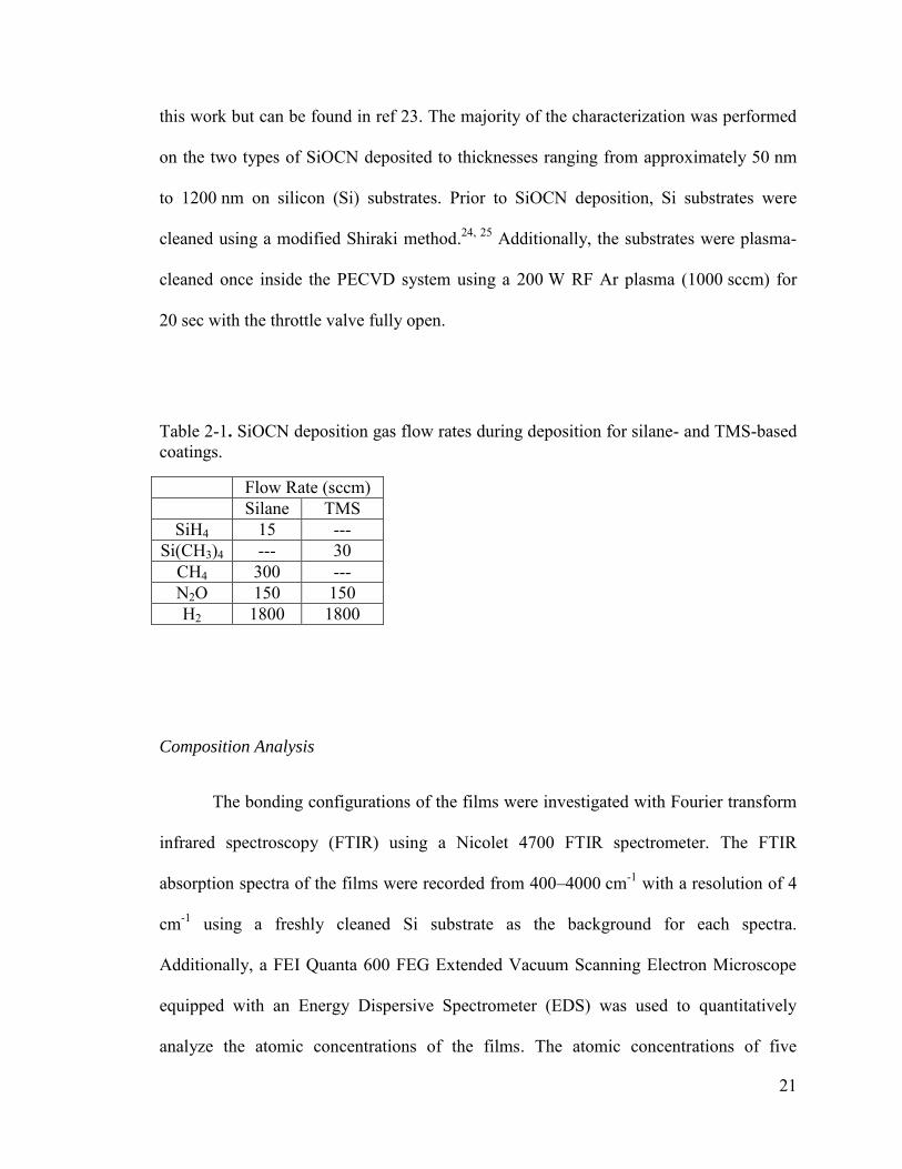
Table 2-1. SiOCN deposition gas flow rates during deposition for silane- and TMS-based coatings. ............................................................................................................................ 21
Table 2-2. FTIR peak assignments. ν=stretching, δ=bending, ρ=rocking, a=asymmetric, s=symmetric ...................................................................................................................... 31
Table 2-3. Dielectric constant (κ), total average breakdown strength (BD), and deposition rate (rd) versus deposition temperature (TD). .................................................................... 35
Table 3-1. List of etch recipes ........................................................................................... 60
Table 4-1. List of investigated ILs and concentrations (v/v) of Ag or Au........................ 76
Table 4-2. Generalization of the resulting particles sizes. L denotes that large particles were formed, and S denotes that the particles remained small and separated. ................. 86
Table 5-1. CV Voltage windows measured at least 3 weeks after metal deposition ...... 105
Table 5-2. Parameters used to plot within the Waldon plot. Values were taken from the manufacturer unless specified otherwise. ....................................................................... 112
xii
Abstract The growing need for energy to be stored in decreasing volumes has resulted in
extensive amounts of research into materials chemistry, new fabrication techniques, and
the utilization of nano-materials. In this investigation, we have extensively characterized
two nanocomposite materials for potential use within energy storage devices. The first
nanocomposite is a silicon oxycarbonitride (SiOCN) film grown by plasma enhanced
chemical vapor deposition which demonstrates low leakage current, high breakdown
strength (>7 MV cm-1), low roughness (<0.7 nm), low stress, and superb chemical
inertness, making it an ideal candidate for use as a dielectric in thin film capacitors.
Utilizing this SiOCN material, a technique has been developed to fabricate one-, two-,
and three-layer thin film capacitors by highly selective etching techniques. The technique
demonstrates the ability to fabricate devices with different numbers of active capacitive
layers with the same number of steps.
The second nanocomposite is a sputtered nanoparticle-in-ionic liquid colloid.
Careful investigations into the deposited nanoparticle growth mechanism and resulting
electrochemical properties suggest anions with more localized charges provide increased
stability and produce single crystal particles and provide increased electrochemical
performance (e.g. up to a 53% increase in potential window, 4.2x increase in ionic
conductivity, 2.9x increase in double-layer capacitance), while less localized charges
promote coalescence and do not provide enhanced electrochemical behavior. These
properties suggest prospective use as electrolytes for increase energy and power density
within electrochemical double layer capacitors, as well as improved performance in ionic
liquid based solar cells and sensors.
1
Chapter 1 – Introduction
Energy storage devices are necessary to meet the ever increasing energy
demands of the world. Electronic devices are getting smaller all the time, and energy
storage devices need to follow suit. Although there are many types of energy storage
devices that are receiving extensive attention, this work will focus on capacitors – both
dielectric capacitors and electrochemical double layer capacitors – and the incorporation
and application of nanotechnology towards current and future advancements.
As opposed to other forms of energy storage – such as fuel cells, and batteries
– capacitors exhibit superior power density. Power density is defined as the rate at which
energy can be put into or released from the device per unit volume. In other words, for
the same amount of energy density (the amount of energy stored per unit volume),
capacitors can charge and discharge at a much faster rate than batteries. Although this
characteristic is desired for some applications in which fast discharge is needed, such as
pulsed power applications, it is easy to see that it is highly desired for the fast charging
rate. For example, current battery-operated devices might take hours to charge, while if
the battery was replaced with capacitor technology it may charge in minutes or less.
However, the drawback of capacitors is the significantly inferior energy density. This
means for the same size, capacitors are not able to provide the necessary energy to power
the aforementioned device.
Extensive amounts of research is being performed striving towards the best of
both worlds – high power and high energy – and nanotechnology is a common path for
the attempts to reach this goal. Before discussing some of the ways nanotechnology has
2
impacted capacitor devices, a short description of the basics of capacitors will be
provided.
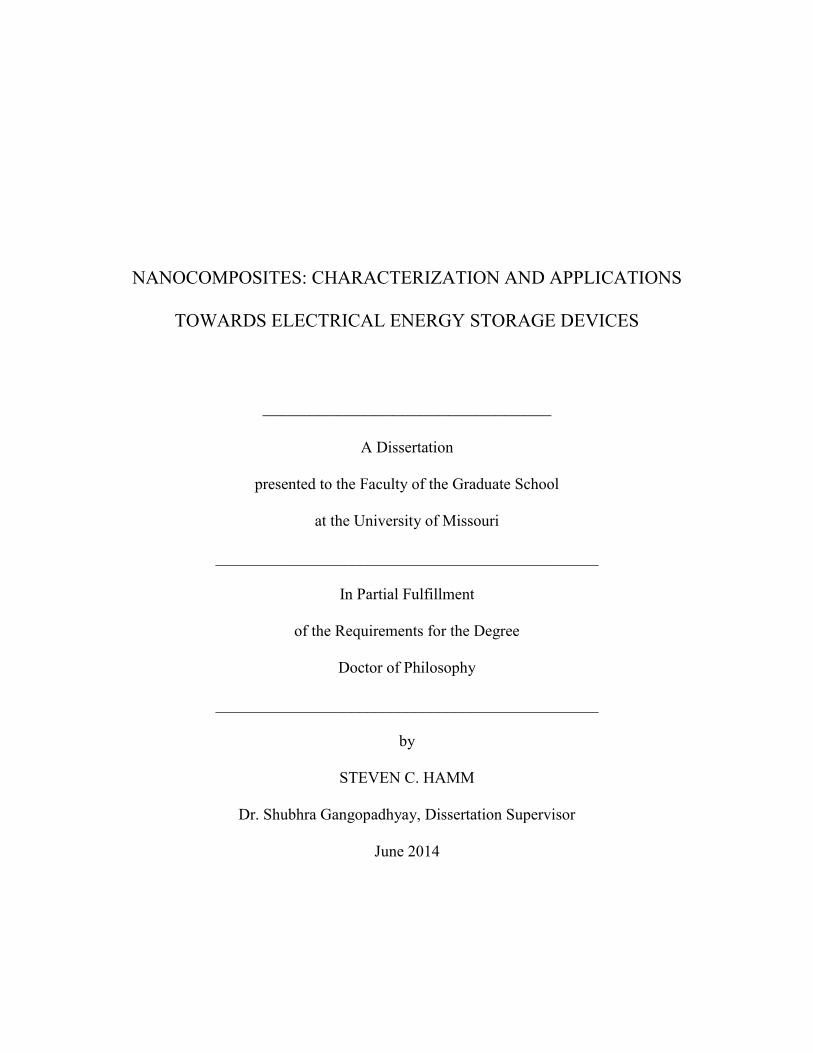
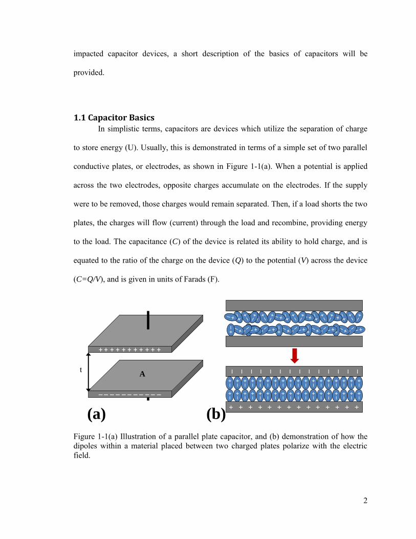
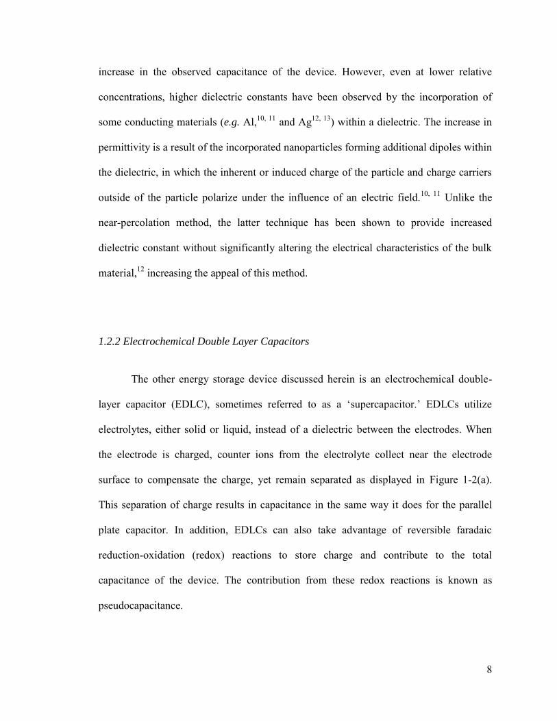
1.1 Capacitor Basics In simplistic terms, capacitors are devices which utilize the separation of charge
to store energy (U). Usually, this is demonstrated in terms of a simple set of two parallel
conductive plates, or electrodes, as shown in Figure 1-1(a). When a potential is applied
across the two electrodes, opposite charges accumulate on the electrodes. If the supply
were to be removed, those charges would remain separated. Then, if a load shorts the two
plates, the charges will flow (current) through the load and recombine, providing energy
to the load. The capacitance (C) of the device is related its ability to hold charge, and is
equated to the ratio of the charge on the device (Q) to the potential (V) across the device
(C=Q/V), and is given in units of Farads (F).
Figure 1-1(a) Illustration of a parallel plate capacitor, and (b) demonstration of how the dipoles within a material placed between two charged plates polarize with the electric field.
t
+ + + + + + + + + + +
– – – – – – – – – – –
A – – – – – – – – – – – – – – – –
++++++++++++++
–+
–+
–+
–+
–+
–+
–+
–+
–+
–+
–+
–+
–+
–+
–+
–+
–+
–+
–+
–+
–+
–+
–+
–+
–+
–+
–+
–+
–+
–+
–+
–+
–+
–+
–+
–+
–+
–+
–+
–+
–+
(a) (b)
3
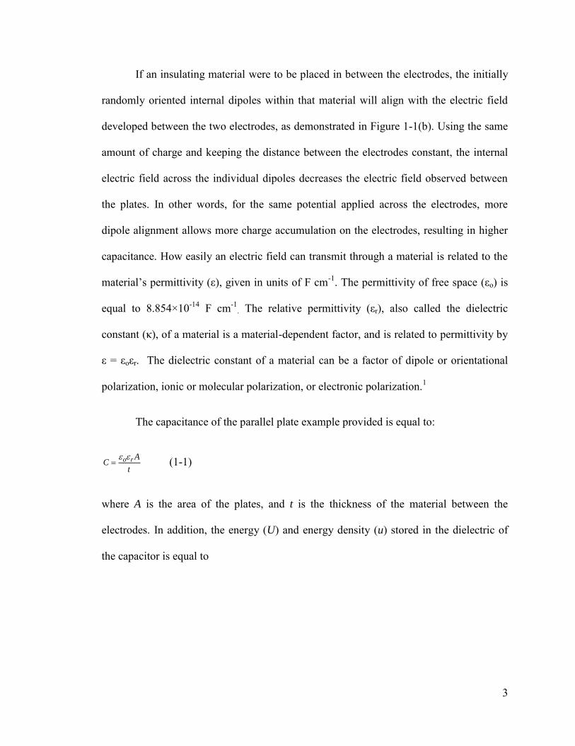
If an insulating material were to be placed in between the electrodes, the initially
randomly oriented internal dipoles within that material will align with the electric field
developed between the two electrodes, as demonstrated in Figure 1-1(b). Using the same
amount of charge and keeping the distance between the electrodes constant, the internal
electric field across the individual dipoles decreases the electric field observed between
the plates. In other words, for the same potential applied across the electrodes, more
dipole alignment allows more charge accumulation on the electrodes, resulting in higher
capacitance. How easily an electric field can transmit through a material is related to the
material’s permittivity (ε), given in units of F cm-1. The permittivity of free space (εo) is
equal to 8.854×10⁻¹⁴ F cm-1. The relative permittivity (εr), also called the dielectric
constant (κ), of a material is a material-dependent factor, and is related to permittivity by
ε = εoεr. The dielectric constant of a material can be a factor of dipole or orientational
polarization, ionic or molecular polarization, or electronic polarization.1
The capacitance of the parallel plate example provided is equal to:
o r AC
t
(1-1)
where A is the area of the plates, and t is the thickness of the material between the
electrodes. In addition, the energy (U) and energy density (u) stored in the dielectric of
the capacitor is equal to
4
212
U CV (1-2)
212 o ru E (1-3)
where V is the applied voltage, and E is the electric field observed across the dielectric (E
= V/t). As can be seen in the previous equations, to increase the energy density of the
device, the dielectric constant of the material in between the electrodes must increase, the
applied potential must increase, or the distance between the electrodes must decrease.
Although the equations make increasing the energy density appear easy, inherent
material properties significantly limit these possibilities. First of all, dielectric materials
can only withstand a set amount of electric field before it reaches failure, known as
electrical breakdown strength (EBD), resulting in a short between the two electrodes. In
other words, you can only decrease the dielectric thickness or increase the applied
potential to the determined material-dependent amount before the device fails. To
complicate things ever more, the breakdown strength is inversely proportional to the
dielectric constant of a material, with a relationship proportional to approximately (κ)-0.5.2
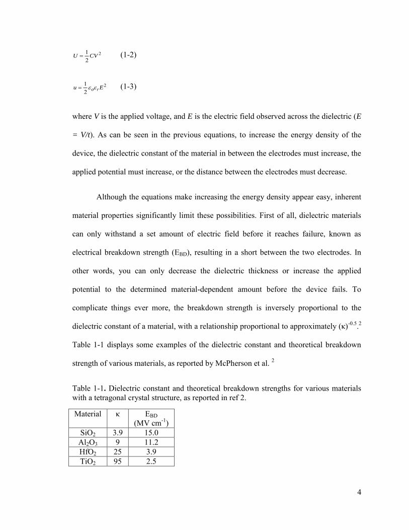
Table 1-1 displays some examples of the dielectric constant and theoretical breakdown
strength of various materials, as reported by McPherson et al. 2
Table 1-1. Dielectric constant and theoretical breakdown strengths for various materials with a tetragonal crystal structure, as reported in ref 2.
Material κ EBD (MV cm-1)
SiO2 3.9 15.0 Al2O3 9 11.2 HfO2 25 3.9 TiO2 95 2.5
5
1.2 Nanocomposites within Capacitors Nanocomposites, which by definition are materials or combinations of
materials in which at least one of the constituent’s dimensions is on the nanometer scale
(<100 nm), are being increasingly explored as materials to meet the energy storage needs
of future capacitors and electrochemical double-layer capacitors (EDLCs). Some
examples of current investigations utilizing nanocomposite materials within dielectric
capacitors and EDLCs will be provided below.
1.2.1 Dielectric Capacitors
Dielectric capacitors, like the parallel plate example described earlier, are energy
storage devices that are used in applications ranging from pulsed power to signal filters.
Regardless of the application, there is great need to reduce the size (increase energy
density), whether it is for more easily deployable weapon systems or to decrease the size
and weight of circuit boards in electronic devices. Although dielectric capacitors are
utilized in such a variety of applications, this work will focus on increasing the energy
density of capacitors used in integrated circuits or on circuit boards.
Current surface-mount capacitors used on circuit boards are fabricated through
ceramic processes. In short, a ceramic slurry made of dielectric particles is made into
sheets, which are screen printed with electrodes from a metal slurry and stacked
numerous times. The stacked material is then pressed and diced into individual
capacitors, followed by firing and a process to connect the electrodes.3, 4 Significant
improvements have been made to the fabrication process to achieve capacitors that are
now 1 million times smaller than the same capacitance values achieved in 1961, an
6
achievement reached by investigating different materials and developing methods to
decrease the thickness of the ceramic slabs.
One signficant contribution to the decrease in size is a result of decreased particle
size used within the slurries. Using smaller particles, such as those on the nanometer
scale, improves the capacitors in a number of ways. Smaller particles result in smoother
ceramic slabs, which levels the electric field observed across the dielectric area. In
contrast, rough layers cause increased electric fields at the peaks of the rough surface,
inducing increased leakage current and decreased voltage capabilities.3 In addition,
smaller particles reduce the void fraction observed in the dielectric and metal layers.
These defects within the layers cause increases in leakage current, decrease the
breakdown strength of the device, and result in decreased reliability.3
To obtain next generation devices with even greater reliability and smaller size,
new fabrication methods should be investigated. Thin film deposition techniques, such as
physical vapor deposition (PVD) and chemical vapor deposition (CVD) methods, have
the ability to deposit very smooth, dense films. Another advantage of using thin film
fabrication techniques is the ability to form the multilayer capacitors on three
dimensional substrates. These capacitors, sometimes called trench capacitors,5 are
gaining increasing interest for use within integrated circuits since these capacitors
efficiently utilize the underlying substrate to achieve larger capacitances without
increasing the total footprint size.6-9 These qualities make thin film deposition techniques
a very appealing alternative to current methods. However, typical thin film capacitor
fabrication techniques are disadvantageous and costly because they require a large
number of fabrication steps. To overcome this issue, a process which fabricated
7
multilayer thin film capacitors utilizing the same number of fabrication steps despite the
number of layers, and which can be transferred to processes for the formation of
capacitors on three-dimensional substrates was developed and elaborated on in Chapter 3.
Although the use of nanomaterials to achieve enhancments in relative permitivity
are not a topic of this work, it is worth mentioning a couple methods for the sake of
elaboration. Nanotechnology has received a lot of interest in the pursuit of increasing the
dielectric constant of materials as a consequence of the interesting and superior properties
some nanoparticles exhibit compared to their bulk counterparts. For instance, thin film
barium titanate has a dielectric constant less than 500, while fabricated <100 nm particles
can achieve dielectric constants greater than 10,000.5 Similar ultra-high dielectric
constant nanoparticle fillers have been incorporated into high dielectric strength polymers
in an attempt to achieve films with increased energy density. This process has achieved
increasing success, achieving energy densities 42.9% higher than the base polymers.6
This approach appears to be promising for polymer-based dielectrics, which are
appealing for low temperature-based fabrication methods.
In addition, conducting nanoparticles have been incorporated into various media
resulting in increased dielectric constant.7-13 Depending on the concentration of the
nanoparticles, the enhanced dielectric constant is a result of different factors. At high
concentrations just below percolation (the concentration at which the particles will form a
conducting path between the electrodes), the particles cluster and propagate from the
electrodes, effectively acting as extensions of the electrode.7-9 This near-percolation
effect results in large concentrations of parallel particle clusters, and consequently can be
viewed as a parallel capacitor network with minimal thickness, causing a significant
8
increase in the observed capacitance of the device. However, even at lower relative
concentrations, higher dielectric constants have been observed by the incorporation of
some conducting materials (e.g. Al,10, 11 and Ag12, 13) within a dielectric. The increase in
permittivity is a result of the incorporated nanoparticles forming additional dipoles within
the dielectric, in which the inherent or induced charge of the particle and charge carriers
outside of the particle polarize under the influence of an electric field.10, 11 Unlike the
near-percolation method, the latter technique has been shown to provide increased
dielectric constant without significantly altering the electrical characteristics of the bulk
material,12 increasing the appeal of this method.
1.2.2 Electrochemical Double Layer Capacitors
The other energy storage device discussed herein is an electrochemical double-
layer capacitor (EDLC), sometimes referred to as a ‘supercapacitor.’ EDLCs utilize
electrolytes, either solid or liquid, instead of a dielectric between the electrodes. When
the electrode is charged, counter ions from the electrolyte collect near the electrode
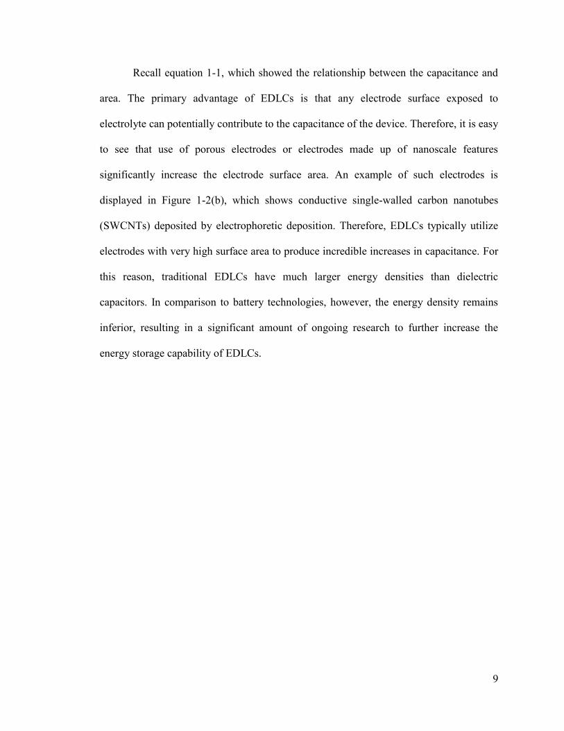
surface to compensate the charge, yet remain separated as displayed in Figure 1-2(a).
This separation of charge results in capacitance in the same way it does for the parallel
plate capacitor. In addition, EDLCs can also take advantage of reversible faradaic
reduction-oxidation (redox) reactions to store charge and contribute to the total
capacitance of the device. The contribution from these redox reactions is known as
pseudocapacitance.
9
Recall equation 1-1, which showed the relationship between the capacitance and
area. The primary advantage of EDLCs is that any electrode surface exposed to
electrolyte can potentially contribute to the capacitance of the device. Therefore, it is easy
to see that use of porous electrodes or electrodes made up of nanoscale features
significantly increase the electrode surface area. An example of such electrodes is
displayed in Figure 1-2(b), which shows conductive single-walled carbon nanotubes
(SWCNTs) deposited by electrophoretic deposition. Therefore, EDLCs typically utilize
electrodes with very high surface area to produce incredible increases in capacitance. For
this reason, traditional EDLCs have much larger energy densities than dielectric
capacitors. In comparison to battery technologies, however, the energy density remains
inferior, resulting in a significant amount of ongoing research to further increase the
energy storage capability of EDLCs.
10
Figure 1-2. (a) A simplified illustration demonstrating the charge separation and storage within an EDLC, and (b) photograph of SWCNT electrode deposited by electrophoretic deposition for an EDLC with and an example of an SEM image of the SWCNTs.
As just discussed, nanotechnology has an inherently significant role in EDLCs. It
is worth noting that it has recently been shown that optimization of the electrode pore
size is necessary to obtain maximum energy density.14, 15 These reports indicate that the
pore size should be approximately the same dimension as the ion size for the maximum
capacitance. In addition, MnO2,17 Fe2O3,16 and RuO2 17 are popular electrode
nanomaterials within EDLCs for enhancement in the energy density due to
psuedocapacitance. These materials have been investigated as independent high surface
area nanostructured electrodes as well as nanoscale decorations on high surface area
conducting electrodes. 17, 18
––––––––
+
+
+
+
+
+
+
+
+
+
+
–
–
–
–
––
Electrolyte
1 µm
(a) (b)
11
Despite the significant interest in nanomaterials for electrodes, there are far less
investigations into utilizing nanoparticles within the EDLC electrolyte. One of the more
popular investigations is utilizing silica nanoparticles within lithium ion–ionic liquid
electrolytes for lithium battery–EDLC hybrid devices or within lithium ion batteries
using the ionic liquid as a solvent.17-21 One primary issue with EDLCs is that many
liquid-based electrolytes are volatile, flammable, and have low potential windows. As
will be elaborated on in Chapter 4 and 5, ionic liquids are excellent electrolyte materials
because they do not have these issues, providing potential improvements in longevity and
energy density of the devices. The anions from the lithium salt and ionic liquid in these
hybrid electrolyte systems have been found to agglomerate with the Li+ ion, and therefore
prevent the Li+ ion from interacting with the electrode. However, the incorporation of
silica nanoparticles, which have an inherent hydroxyl-terminated surface, forms hydrogen
bonds with anions, subsequently freeing Li+ ions.17, 18 Metal nanoparticles within ionic
liquid electrolytes, such as those investigated in this work, have received even less
attention. One exemplary example investigated freely suspended AuNPs in IL which
demonstrated quantized charging behavior.22
Upon initial investigation of the electrochemical properties of the IL electrolyte 1-
ethyl-3-methylimidazolium bis(trifluoromethylsulfonyl)imide with sputter deposited
metal nanoparticles, it was observed that there was increased electrochemical window
and double-layer capacitance when compared to the IL without the nanoparticles. The
rather perplexing enhancements is what instigated the investigation of the metal
nanoparticle growth (Chapter 4) as well as a more detailed investigation towards the
electrochemical properties (Chapter 5) of metal nanoparticles in a variety of ionic liquids.
12
The motivation of these investigations was to develop a theory for the cause of the
enhancements, so that a future direction could be provided towards even more
enhancement and prolonged permanence.
Regardless of the nanocomposite material, it is important to understand the
fundamental characteristics and even the growth mechanisms to investigate the potential
use within energy storage devices and provide possible future improvement. On this end,
this dissertation will cover the characterization and applications of two nanocomposite
materials towards energy storage devices. A detailed description of the work provided
herein is described in the following section
.
13
1.3 Scope of the Dissertation
This dissertation is divided into five chapters discussing different investigated
nanocomposite materials and their inherent characteristics, as well as their applications
toward energy storage devices. Chapter 2 reviews a nanocomposite silicon
oxycarbonitride (SiOCN) thin film grown by plasma-enhanced chemical vapor deposition
(PECVD). Understanding the film compositional, electrical, and mechanical properties is
important in determining the applicability of the material towards use within thin film
capacitors.
Chapter 3 describes the development and results of a process to fabricate thin
film multilayer capacitors. Novel thin film capacitor fabrication techniques are needed in
order to further miniaturize current electronics by integrating passive components within
the circuit board itself. A great challenge to this is finding an appropriate method which
provides a time and cost effective process. The fabrication steps and the device
characterization will be discussed utilizing the SiOCN dielectric and the highly selective
etching capabilities of two metals.
Chapter 4 focuses on the growth mechanisms of sputter deposited metal
nanoparticles in ionic liquids. This process poses as a potentially cleaner method of
fabricating nanoparticles in that it does not require reducing or structure forming agents,
or results in byproducts formed by conventional wet chemistry means. In addition to
supplying a theory for the growth mechanisms of metal nanoparticles within the liquid,
suggestions are provided for other researchers utilizing this method for more controlled
14
experiments to investigate the growth. The theory developed in this chapter precedes the
theory discussed in Chapter 5.
Chapter 5 provides electrochemical analysis of the nanoparticle-in-ionic liquid
composites from Chapter 4 utilizing cyclic voltammetry and electrochemical impedance
spectroscopy as a function of time after deposition. Based on the evidence provided, a
theory is developed to describe the observed changes in the electrochemical properties of
the electrolyte, providing potential avenues towards the further enhancement and
increased longevity of the characteristics.
To wrap up, Chapter 6 will provide an overview of the major conclusions derived
from the work and provide direction for potential future work.
15
1.4 References
1. Balanis, C. A., Engineering Electromagnetics. Wiley: 1989.
2. McPherson, J. W.; Jinyoung, K.; Shanware, A.; Mogul, H.; Rodriguez, J., Trends in the ultimate breakdown strength of high dielectric-constant materials. IEEE Trans.
Electron Devices 2003, 50, 1771-1778.
3. Samantaray, M. M.; Gurav, A.; Dickey, E. C.; Randall, C. A., Electrode Defects in Multilayer Capacitors Part I: Modeling the Effect of Electrode Roughness and Porosity on Electric Field Enhancement and Leakage Current. J. Am. Ceram. Soc. 2012, 95, 257-263.
4. Kishi, H.; Mizuno, Y.; Chazono, H., Base-metal electrode-multilayer ceramic capacitors: past, present and future perspectives. Jpn. J. Appl. Phys. 2003, 42, 1-15.
5. Klootwijk, J. H.; Jinesh, K. B.; Dekkers, W.; Verhoeven, J. F.; Van Den Heuvel, F. C.; Kim, H. D.; Blin, D.; Verheijen, M. A.; Weemaes, R. G. R.; Kaiser, M.; Ruigrok, J.; Roozeboom, F., Ultrahigh Capacitance Density for Multiple ALD-Grown MIM Capacitor Stacks in 3-D Silicon. IEEE Electron Device Lett. 2008, 29, 740-742.
6. Detalle, M.; Barrenetxea, M.; Muller, P.; Potoms, G.; Phommahaxay, A.; Soussan, P.; Vaesen, K.; De Raedt, W., High density, low leakage Back-End 3D capacitors for mixed signals applications. Microelectron. Eng. 2010, 87, 2571-2576.
7. Banerjee, P.; Perez, I.; Henn-Lecordier, L.; Lee, S. B.; Rubloff, G. W., Nanotubular metal–insulator–metal capacitor arrays for energy storage. Nat.
Nanotechnol. 2009, 4, 292-296.
8. Banerjee, P.; Perez, I.; Henn-Lecordier, L.; Lee, S. B.; Rubloff, G. W., ALD based Metal-insulator-metal (MIM) Nanocapacitors for Energy Storage. ECS Trans.
2009, 25, 345-353.
9. Nongaillard, M.; Lallemand, F.; Allard, B., Design for manufacturing of 3D capacitors. Microelectron. J. 2010, 41, 845-850.
10. Wada, S.; Kondo, S.; Moriyoshi, C.; Kuroiwa, Y., Preparation of highly dispersed barium titanate nanoparticles from barium titanyl oxalate nanoparticles and their
16
dielectric properties. Japanese Journal of Applied Physics-Part 1Regular Papers and
Short Notes 2008, 47, 7612.
11. Tang, H.; Sodano, H. A., Ultra High Energy Density Nanocomposite Capacitors with Fast Discharge Using Ba0.2Sr0.8TiO3 Nanowires. Nano Lett. 2013, 13, 1373-1379.
12. Lu, J.; Moon, K.-S.; Xu, J.; Wong, C., Synthesis and dielectric properties of novel high-K polymer composites containing in-situ formed silver nanoparticles for embedded capacitor applications. J. Mater. Chem. 2006, 16, 1543-1548.
13. Lu, J.; Wong, C., Recent advances in high-k nanocomposite materials for embedded capacitor applications. Dielectrics and Electrical Insulation, IEEE
Transactions on 2008, 15, 1322-1328.
14. Xu, J.; Wong, M.; Wong, C. In Super high dielectric constant carbon black-filled
polymer composites as integral capacitor dielectrics, Electronic Components and Technology Conference, 2004. Proceedings. 54th, IEEE: 2004; pp 536-541.
15. Jianwen, X.; Wong, C. P. In Effects of the low loss polymers on the dielectric
behavior of novel aluminum-filled high-k nano-composites, Int. Symp. Adv. Packag. Mater.: Processes, Prop. Interfaces, 9th., 2004; 2004; pp 158-170.
16. Jianwen, X.; Kyoung-Sik, M.; Tison, C.; Wong, C. P., A novel aluminum-filled composite dielectric for embedded passive applications. Advanced Packaging, IEEE
Transactions on 2006, 29, 295-306.
17. Ravindran, R.; Gangopadhyay, K.; Gangopadhyay, S.; Mehta, N.; Biswas, N., Permittivity enhancement of aluminum oxide thin films with the addition of silver nanoparticles. Appl. Phys. Lett. 2006, 89, 263511-263511-3.
18. Saha, S., Observation of giant dielectric constant in an assembly of ultrafine Ag particles. Physical Review B 2004, 69, 125416.
19. Largeot, C.; Portet, C.; Chmiola, J.; Taberna, P.-L.; Gogotsi, Y.; Simon, P., Relation between the Ion Size and Pore Size for an Electric Double-Layer Capacitor. J.
Am. Chem. Soc. 2008, 130, 2730-2731.
17
20. Lin, R.; Huang, P.; Ségalini, J.; Largeot, C.; Taberna, P. L.; Chmiola, J.; Gogotsi, Y.; Simon, P., Solvent effect on the ion adsorption from ionic liquid electrolyte into sub-nanometer carbon pores. Electrochim. Acta 2009, 54, 7025-7032.
21. Lee, J. S.; Shin, D. H.; Jun, J.; Lee, C.; Jang, J., Fe3O4/Carbon Hybrid Nanoparticle Electrodes for High-Capacity Electrochemical Capacitors. ChemSusChem
2014, n/a-n/a.
22. Saito, Y.; Umecky, T.; Niwa, J.; Sakai, T.; Maeda, S., Existing Condition and Migration Property of Ions in Lithium Electrolytes with Ionic Liquid Solvent. J. Phys.
Chem. B 2007, 111, 11794-11802.
23. Umecky, T.; Saito, Y.; Okumura, Y.; Maeda, S.; Sakai, T., Ionization Condition of Lithium Ionic Liquid Electrolytes under the Solvation Effect of Liquid and Solid Solvents. J. Phys. Chem. B 2008, 112, 3357-3364.
24. Unemoto, A.; Iwai, Y.; Mitani, S.; Baek, S.-W.; Ito, S.; Tomai, T.; Kawamura, J.; Honma, I., Electrical conductivity and dynamics of quasi-solidified lithium-ion conducting ionic liquid at oxide particle surfaces. Solid State Ionics 2011, 201, 11-20.
25. Unemoto, A.; Iwai, Y.; Mitani, S.; Baek, S.-W.; Ito, S.; Tomai, T.; Kawamura, J.; Honma, I., Mass transport properties in quasi-solidified lithium-ion conducting ionic liquids at oxide particle surfaces. Solid State Ionics 2012, 225, 416-419.
26. Sun, J.; Bayley, P.; MacFarlane, D.; Forsyth, M., Gel electrolytes based on lithium modified silica nano-particles. Electrochim. Acta 2007, 52, 7083-7090.
27. Mertens, S. F.; Vollmer, C.; Held, A.; Aguirre, M. H.; Walter, M.; Janiak, C.; Wandlowski, T., “Ligand‐Free” Cluster Quantized Charging in an Ionic Liquid. Angew.
Chem. Int. Ed. 2011, 50, 9735-9738.
18
Chapter 2 – Characterization of SiOCN Grown by PECVD towards
use in Thin Film Capacitors
2.1 Introduction
A good candidate for thin film capacitors must meet a number of requirements.
First, the material should have low leakage current and high breakdown strength, to
reduce loss and offer enhanced energy density. Second, the film should preferably have a
low residual stress so that the film can be deposited to large thicknesses, providing high
voltage capability. Third, the material should be very smooth and dense, as elaborated on
in Chapter 1. Finally, the material should have adequate chemical inertness, so that it is
impervious to the various etchants required in the thin film capacitor microelectronic
fabrication steps.
Plasma-enhanced chemical vapor deposition (PECVD) is a highly desirable
technique to deposit a material to meet these needs due to the ability to deposit quality
films at moderate-to-low temperatures, while offering relatively easy tunability of the
resulting film by changing the deposition parameters. Many of the characteristics and
growth mechanisms of PECVD deposited silicon-based films (e.g. SiO2, SiC, Si3N4,
SiCN) have been extensively studied and have found use as dielectrics,1-3 within
waveguides and other optical devices,4 as barrier layers,5 as well as many other
applications.6 However, excepting a small number of investigations using PECVD grown
SiOCN within electronics or studying the hardness and growth 6-9, there are still very few
studies on this material and its properties, rendering its future applicability undetermined.
19
One of the recurring issues with films deposited by PECVD is the incorporation
of hydrogen, particularly at low deposition temperatures (e.g. in the form of Si–H, Si–
OH, Si–CH3, etc.). Hydrogen is typically known to be detrimental towards a number of
electrical, optical, and mechanical properties due to the disruption of the molecular order
within the films (i.e. the introduction of pores, defect states, and CHx polymeric-like
components). For example, hydrogen incorporation is known to decrease dielectric
constant, breakdown strength, hardness, refractive index, and increase leakage current, to
name a few. 10-12
A post-deposition anneal at increased temperatures is a common method to
decrease the hydrogen concentration within a PECVD grown film. However, to maintain
the versatility of the coating and the possible substrates which can be used, this method is
undesirable. Therefore, a more attractive method is the use of hydrogen as a dilution gas
during the deposition. Hydrogen dilution has been observed to have high reactivity with
hydrogen-containing groups and other weak bonds, effectively acting as an etching
mechanism in competition with the deposition of the film.13, 14 Examples of hydrogen
dilution can be seen extensively in PECVD grown Si,14, 15 SiC,13, 16-18 SiN,19, 20 as well as
other Si alloys.21 In conjunction with the optimization of other deposition parameters,
hydrogen dilution has been observed to decrease the total hydrogen concentration in
PECVD grown films, and/or promote higher molecular order with decreased
concentrations of defects and voids, and increased atomic density.19 In addition, hydrogen
dilution has also shown evidence of increasing the concentration of reactive species
within the plasma, facilitating the formation of bonds not readily formed otherwise.22
20
This work investigates the temperature-dependent growth and potentially
applicable characteristics of the extremely versatile silicon oxycarbonitride (SiOCN) thin
films towards thin film capacitors. The purpose of developing these SiOCN film was to
utilize the same process which could be used for a wide variety of applications, such as a
high voltage insulator, or as a material which could be used as a mask or structure within
microelectronic fabricated devices. These films were grown by PECVD using two sets of
precursors at growth temperatures ranging from 100 °C to 400 °C using hydrogen
dilution. The films were investigated using electron dispersive spectroscopy (EDS),
Fourier Transform Infrared (FTIR) spectroscopy, electrical measurements, atomic force
microscopy, and stress measurements. Further characterization and applications of the
material can be found in Appendix A.
2.2 Materials and Methods
Deposition
SiOCN was deposited at temperatures of 100 °C, 250 °C, and 400 °C using an
Applied Materials Precision 5000 PECVD tool at a chamber pressure of 7 Torr and RF
(13.56 MHz) power of 400 W. Two types of SiOCN were investigated using silane and
tetramethylsilane (TMS) precursors, from now on referred to as silane- and TMS-based
SiOCN, respectively. The precursors and corresponding gas flow rates for each type are
displayed in Table 2-1. These parameters were chosen so that the resulting film had low
hydrogen concentration for optimized characteristics, including high hardness and
electrical breakdown strength. The details of the gas optimization will not be discussed in
21
this work but can be found in ref 23. The majority of the characterization was performed
on the two types of SiOCN deposited to thicknesses ranging from approximately 50 nm
to 1200 nm on silicon (Si) substrates. Prior to SiOCN deposition, Si substrates were
cleaned using a modified Shiraki method.24, 25 Additionally, the substrates were plasma-
cleaned once inside the PECVD system using a 200 W RF Ar plasma (1000 sccm) for
20 sec with the throttle valve fully open.
Table 2-1. SiOCN deposition gas flow rates during deposition for silane- and TMS-based coatings.
Flow Rate (sccm) Silane TMS
SiH4 15 --- Si(CH3)4 --- 30
CH4 300 --- N2O 150 150 H2 1800 1800
Composition Analysis
The bonding configurations of the films were investigated with Fourier transform
infrared spectroscopy (FTIR) using a Nicolet 4700 FTIR spectrometer. The FTIR
absorption spectra of the films were recorded from 400–4000 cm-1 with a resolution of 4
cm-1 using a freshly cleaned Si substrate as the background for each spectra.
Additionally, a FEI Quanta 600 FEG Extended Vacuum Scanning Electron Microscope
equipped with an Energy Dispersive Spectrometer (EDS) was used to quantitatively
analyze the atomic concentrations of the films. The atomic concentrations of five
22
randomly selected locations on the ~1000–1200 nm thick films were analyzed under an
acceleration voltage of 10 kV, which was the minimum voltage required to obtain
consistent results and should sample the bulk of the film with minimal influence of the Si
substrate.
Electrical Characterization
Electrical characterization was performed on SiOCN deposited on heavily doped
n(100) Si substrates (0.001 – 0.002 Ωcm) which were used as the bottom electrode of the
devices. The top electrode, tantalum, was deposited to 100 nm through a shadow mask by
sputter deposition at a chamber pressure of 4 mTorr, 200 W DC power, and Ar flow rate
of 20 sccm. Device areas of 0.196 mm2 were used to study dielectric constant, leakage
current (resistivity), and breakdown strength of the films. An Agilent 4284A LCR Meter
was used to study the dielectric constant of the ~480–600 nm thick films using
capacitance–voltage (C–V) measurements taken at 1 kHz. The electrical resistivities of
the films were measured in a Signatone probe station enclosure with N2 atmosphere using
a Keithley 4200 SCS. The resistivities were calculated from the slopes of the leakage
current at low applied potentials (<0.1 MV cm-1) using voltage steps of ~1 kV cm-1 with a
delay of 12 seconds between subsequent measurements. Finally, the dielectric breakdown
strength of the SiOCN films were tested using current–voltage (I–V) measurements using
a Keithley 6487 Picoammeter and a Keithley 248 High Voltage Power Supply with a
2.4 MΩ series resistor to protect the equipment at the time of failure. The voltage was
applied to the Si substrate and was increased from 0 with a voltage step of 2 V until
breakdown was reached, holding the voltage for approximately 2 s before each step due
to the time delay from system communications.
23
Mechanical Characterization
Stress measurements were performed using a Tencor FLX 3000 laser deflection
radius of curvature tool at room temperature, therefore the stress measured is a sum of
the extrinsic and intrinsic stresses. The radius of curvature of Si was measured before
and after SiOCN deposition on a four inch Si substrate in four different positions. The
film stress (σf) was calculated using Stoney’s method:26
2
2 1
1 1( )6 (1 )
s sf
f s
E t
t R R
(2-1)
Where Es is the Young’s modulus for the Si wafer (130 GPa),27 ts is the substrate
thickness (525 μm), tf is the film thickness, νs is Poisson’s ratio for the Si wafer (0.28),28
and R1 and R2 are the measured radii of curvature before and after deposition,
respectively.
2.3 Results and Discussion
EDS
The semi-quantitative atomic concentrations were calculated from the EDS data
and plotted in Figure 2-1. Both types of SiOCN have comparable silicon (Si)
concentrations (TMS 26.7–29.3 at.%, silane 26.6–27.8 at.%), which remain relatively
unchanged with increasing deposition temperature. However, the incorporated
concentrations of oxygen (O), carbon (C), and nitrogen (N) are dependent on the
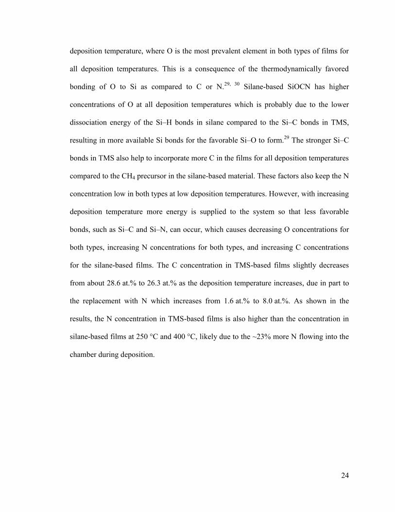
24
deposition temperature, where O is the most prevalent element in both types of films for
all deposition temperatures. This is a consequence of the thermodynamically favored
bonding of O to Si as compared to C or N.29, 30 Silane-based SiOCN has higher
concentrations of O at all deposition temperatures which is probably due to the lower
dissociation energy of the Si–H bonds in silane compared to the Si–C bonds in TMS,
resulting in more available Si bonds for the favorable Si–O to form.29 The stronger Si–C
bonds in TMS also help to incorporate more C in the films for all deposition temperatures
compared to the CH4 precursor in the silane-based material. These factors also keep the N
concentration low in both types at low deposition temperatures. However, with increasing
deposition temperature more energy is supplied to the system so that less favorable
bonds, such as Si–C and Si–N, can occur, which causes decreasing O concentrations for
both types, increasing N concentrations for both types, and increasing C concentrations
for the silane-based films. The C concentration in TMS-based films slightly decreases
from about 28.6 at.% to 26.3 at.% as the deposition temperature increases, due in part to
the replacement with N which increases from 1.6 at.% to 8.0 at.%. As shown in the
results, the N concentration in TMS-based films is also higher than the concentration in
silane-based films at 250 °C and 400 °C, likely due to the ~23% more N flowing into the
chamber during deposition.
25
Figure 2-1. EDS calculated atomic concentrations for a) Si, b) O, c) C, and d) N. Error bars represent the standard deviation.
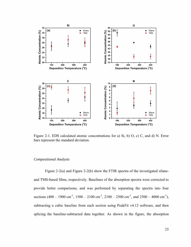
Compositional Analysis
Figure 2-2(a) and Figure 2-2(b) show the FTIR spectra of the investigated silane-
and TMS-based films, respectively. Baselines of the absorption spectra were corrected to
provide better comparisons, and was performed by separating the spectra into four
sections (400 – 1900 cm-1, 1500 – 2100 cm-1, 2100 – 2500 cm-1, and 2500 – 4000 cm-1),
subtracting a cubic baseline from each section using PeakFit v4.12 software, and then
splicing the baseline-subtracted data together. As shown in the figure, the absorption
26
coefficient results reveal similar compositions for both types of SiOCN. The primary
absorption peaks are displayed in the figure and include the following: overlapping Si–C
stretching and Si–O bending modes at 800–810 cm-1,4, 31 Si–H bending mode from H–Si–
O3 at ~885 cm-1,1, 6, 32 Si–O–Si symmetric stretching mode between 1020–1060 cm-1,1, 31
Si–CH3 bending mode located near ~1275 cm-1,1, 31, 33 a peak consisting of closely
overlapping Si–H stretching from H–Si–O3 31, 32, 34 and Si–C≡N 35-37 at around 2250 cm-1,
C–Hx stretching modes between 2830–2970 cm -1,33 N–H stretching at ~3400 cm-1,32, 38
and –OH stretching modes between 3600–3700 cm-1.32, 33, 39 A list of the prominent
absorption modes can also be found in Table 2-2.
27
Figure 2-2. FTIR spectra of SiOCN films growth with (a) silane and (b) TMS precursors at various deposition temperatures.
The corrected spectra were separated in Figure 3 into sections of 600–1500 cm-1
(Figure 2-3(a) and Figure 2-3(b)) and 2050–4000 cm-1 (Figure 2-3(c) and Figure 2-3(d))
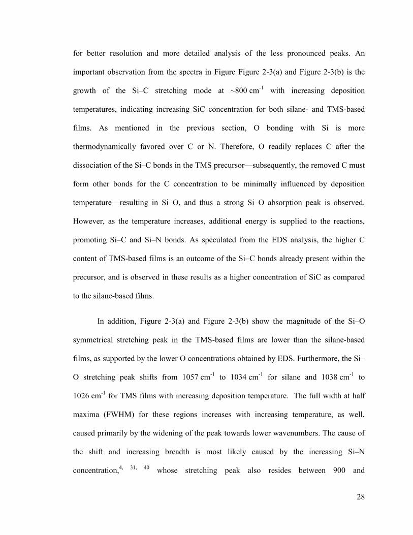
28
for better resolution and more detailed analysis of the less pronounced peaks. An
important observation from the spectra in Figure Figure 2-3(a) and Figure 2-3(b) is the
growth of the Si–C stretching mode at ~800 cm-1 with increasing deposition
temperatures, indicating increasing SiC concentration for both silane- and TMS-based
films. As mentioned in the previous section, O bonding with Si is more
thermodynamically favored over C or N. Therefore, O readily replaces C after the
dissociation of the Si–C bonds in the TMS precursor—subsequently, the removed C must
form other bonds for the C concentration to be minimally influenced by deposition
temperature—resulting in Si–O, and thus a strong Si–O absorption peak is observed.
However, as the temperature increases, additional energy is supplied to the reactions,
promoting Si–C and Si–N bonds. As speculated from the EDS analysis, the higher C
content of TMS-based films is an outcome of the Si–C bonds already present within the
precursor, and is observed in these results as a higher concentration of SiC as compared
to the silane-based films.
In addition, Figure 2-3(a) and Figure 2-3(b) show the magnitude of the Si–O
symmetrical stretching peak in the TMS-based films are lower than the silane-based
films, as supported by the lower O concentrations obtained by EDS. Furthermore, the Si–
O stretching peak shifts from 1057 cm-1 to 1034 cm-1 for silane and 1038 cm-1 to
1026 cm-1 for TMS films with increasing deposition temperature. The full width at half
maxima (FWHM) for these regions increases with increasing temperature, as well,
caused primarily by the widening of the peak towards lower wavenumbers. The cause of
the shift and increasing breadth is most likely caused by the increasing Si–N
concentration,4, 31, 40 whose stretching peak also resides between 900 and
29
1000 cm-1,33, 36, 41, 42 but could also be caused by that of decreasing Si–O–Si angles caused
by increased density.43 The increase in Si–N stretching absorption is a plausible
explanation, then, for the appearance of the growing Si–O symmetrical stretching peak
for the TMS films, despite the O concentration decreasing with increasing deposition
temperature as indicated by the EDS results. In addition, the shoulder located around
1100–1200 cm-1 is representative of the Si–O–Si asymmetrical stretching, as well as
possibly overlapping C–O–C or Si–O–C asymmetric stretching bands.31 Finally, Figure
2-3(a) and Figure 2-3(b) also display that higher deposition temperatures promote the
dissociation of hydrogen bonds, as is observed in the H–Si–O3 and Si–CH3 bending
modes, which tend to decrease with increasing deposition temperature for both types of
films.
Figure 2-3(c) and Figure 2-3(d) show peaks consisting of a convolution of C–Hx
stretching (2830–2970 cm -1),5, 31, 44 N–H stretching (3400 cm-1),32, 33, 38 N–H2
asymmetrical stretching (3500 cm-1),32, 33 and Si–OH (3650 cm-1)32, 33, 39 stretching modes
indicating hydrogen is present in a variety of moieties within the films, albeit at relatively
low concentrations. The Si–OH peak rises sharply at ~3650 cm-1 and has a rather long
tail towards lower wavenumbers, which is typically observed from isolated Si–OH,
where the tail originates from the various bonding strengths and distances of the
hydrogen to surrounding atoms.39 The Si–OH peak for silane is larger than TMS films
because of the larger concentration of O to which the hydrogen can bond. The total
hydrogen concentration decreases with increasing deposition temperature due to the
additional energy provided to dissociate these bonds, as indicated by the decrease in
magnitudes. It is important to note that both film types see an even more pronounced
30
decrease in the peak at 2970 cm-1, which is the asymmetrical stretching mode for sp3 –
CH3.31, 44 The strong decrease in the –OH, –NH2, and –CH3 components is extremely
important because these indicate low concentrations of terminating groups, which would
prevent long-ordered molecular structures and facilitate the formation of voids. In other
words, the results suggest lower porosity and enhanced order with increasing deposition
temperature, which will be demonstrated by other means later. Therefore, the TMS-based
SiOCN is expected to exhibit higher molecular order than silane-based films since they
have lower hydrogen concentrations at the same deposition temperatures.
While the H–Si–O3 bending and stretching peaks at 885 cm-1 and 2250 cm-1,
respectively, decrease with increasing temperature, a strong relationship between the
magnitudes of the peaks between all samples is not observed. We therefore attribute the
peak observed between 2240 cm-1 and 2260 cm-1 to also be representative of Si–C≡N, as
has been reported repeatedly in PECVD SiCN films.9, 35-37, 42 The H–SiO3/Si–C≡N peak
is larger in magnitude within TMS-based films due to the larger concentration of N
within the system during deposition, which may facilitate the formation of CN radicals in
the plasma with the assistance of hydrogen dilution, as was reported by Wu et al.22 We
should also note that the decreasing concentration of H–SiO3, as well as the replacement
of the oxygen with C or N, would also cause a shift of the peak for silane-based films
from 2260 cm-1 to 2240 cm-1 due to the lower electronegativity of C and N.32, 34 The peak
for the TMS films, however, is constant at 2240 cm-1 since it consists of a larger portion
of Si–C≡N.
31
Figure 2-3. Resolved FTIR absorption coefficient spectra ranges for (left) silane- and (right) TMS-based SiOCN films.
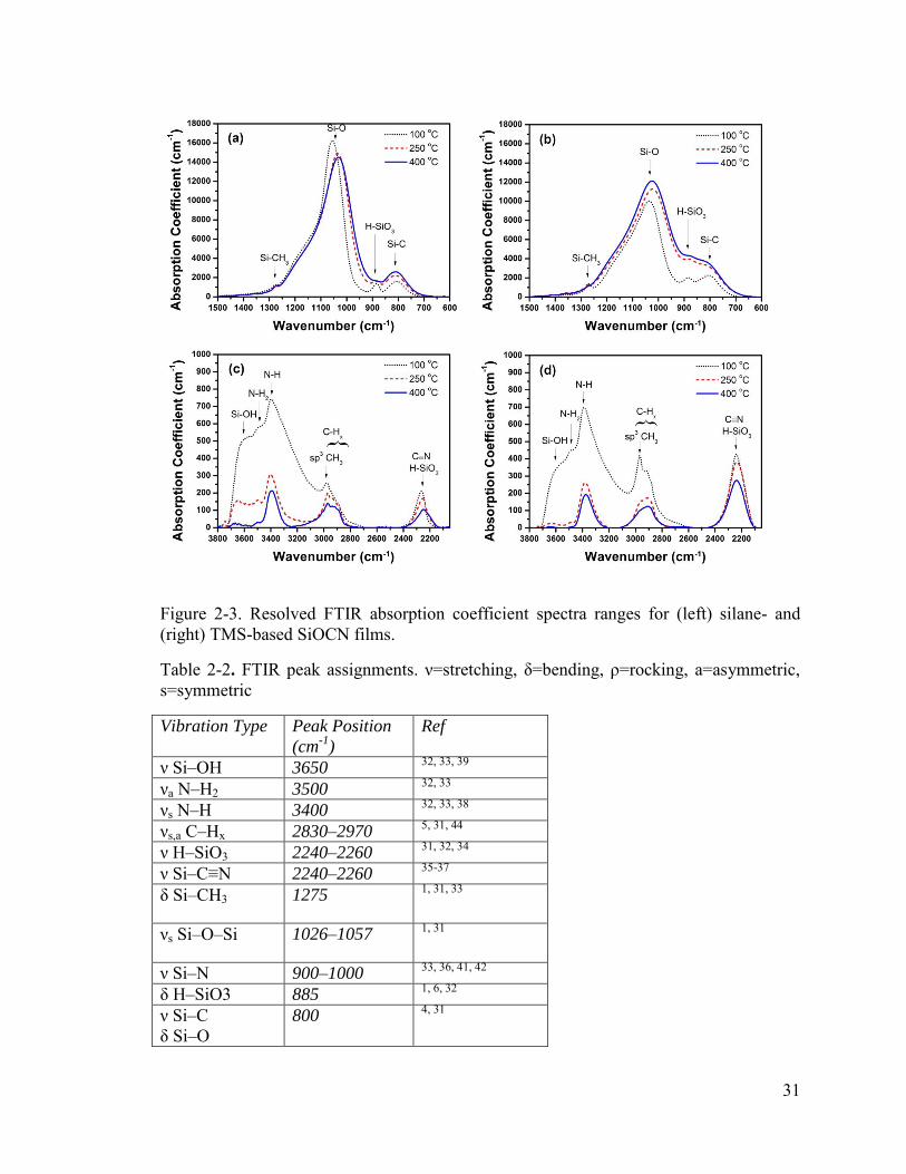
Table 2-2. FTIR peak assignments. ν=stretching, δ=bending, ρ=rocking, a=asymmetric, s=symmetric
Vibration Type Peak Position
(cm-1
)
Ref
ν Si–OH 3650 32, 33, 39
νa N–H2 3500 32, 33
νs N–H 3400 32, 33, 38
νs,a C–Hx 2830–2970 5, 31, 44
ν H–SiO3 2240–2260 31, 32, 34
ν Si–C≡N 2240–2260 35-37
δ Si–CH3 1275 1, 31, 33
νs Si–O–Si 1026–1057 1, 31
ν Si–N 900–1000 33, 36, 41, 42
δ H–SiO3 885 1, 6, 32
ν Si–C δ Si–O
800 4, 31
32
AFM Topography
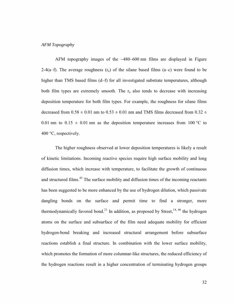
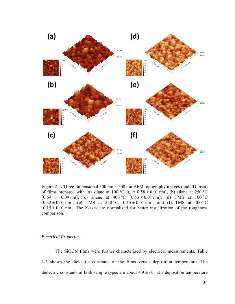
AFM topography images of the ~480–600 nm films are displayed in Figure
2-4(a–f). The average roughness (ra) of the silane based films (a–c) were found to be
higher than TMS based films (d–f) for all investigated substrate temperatures, although
both film types are extremely smooth. The ra also tends to decrease with increasing
deposition temperature for both film types. For example, the roughness for silane films
decreased from 0.58 ± 0.01 nm to 0.53 ± 0.01 nm and TMS films decreased from 0.32 ±
0.01 nm to 0.15 ± 0.01 nm as the deposition temperature increases from 100 °C to
400 °C, respectively.
The higher roughness observed at lower deposition temperatures is likely a result
of kinetic limitations. Incoming reactive species require high surface mobility and long
diffusion times, which increase with temperature, to facilitate the growth of continuous
and structured films.45 The surface mobility and diffusion times of the incoming reactants
has been suggested to be more enhanced by the use of hydrogen dilution, which passivate
dangling bonds on the surface and permit time to find a stronger, more
thermodynamically favored bond.21 In addition, as proposed by Street,14, 46 the hydrogen
atoms on the surface and subsurface of the film need adequate mobility for efficient
hydrogen-bond breaking and increased structural arrangement before subsurface
reactions establish a final structure. In combination with the lower surface mobility,
which promotes the formation of more columnar-like structures, the reduced efficiency of
the hydrogen reactions result in a higher concentration of terminating hydrogen groups
33
(e.g. –OH and –CH3), which promote discontinuous growth and the formation of voids.
Therefore, the roughness is higher for lower deposition temperatures. As the deposition
temperature increases, the terminating bond concentrations decrease and surface mobility
increases resulting in more continuous, i.e. smoother, films. Furthermore, we speculate
that the TMS-based films are smoother than silane-based films because of the slower
diffusion rate of the larger reactive TMS molecule. The slower diffusion for this case
appears advantageous, as it provides more time for the hydrogen atoms from the
hydrogen dilution to break weak bonds and promote more structure within the films.
Therefore, from the average roughness results, we can speculate that the TMS films are
denser than the silane films, and that the density increases with increasing temperature for
both film types.
34
Figure 2-4. Three-dimensional 500 nm × 500 nm AFM topography images (and 2D inset) of films prepared with (a) silane at 100 °C [ra = 0.58 ± 0.01 nm], (b) silane at 250 °C [0.69 ± 0.09 nm], (c) silane at 400 °C [0.53 ± 0.01 nm], (d) TMS at 100 °C [0.32 ± 0.01 nm], (e) TMS at 250 °C [0.15 ± 0.01 nm], and (f) TMS at 400 °C [0.15 ± 0.01 nm]. The Z-axes are normalized for better visualization of the roughness comparison.
Electrical Properties
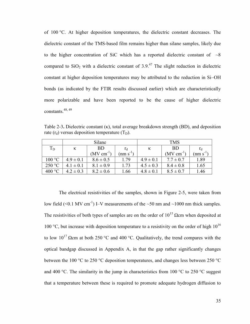
The SiOCN films were further characterized by electrical measurements. Table
2-3 shows the dielectric constants of the films versus deposition temperature. The
dielectric constants of both sample types are about 4.9 ± 0.1 at a deposition temperature
(a)
(b)
(c) (f)
(e)
(d)
35
of 100 °C. At higher deposition temperatures, the dielectric constant decreases. The
dielectric constant of the TMS-based film remains higher than silane samples, likely due
to the higher concentration of SiC which has a reported dielectric constant of ~8
compared to SiO2 with a dielectric constant of 3.9.47 The slight reduction in dielectric
constant at higher deposition temperatures may be attributed to the reduction in Si–OH
bonds (as indicated by the FTIR results discussed earlier) which are characteristically
more polarizable and have been reported to be the cause of higher dielectric
constants.48, 49
Table 2-3. Dielectric constant (κ), total average breakdown strength (BD), and deposition rate (rd) versus deposition temperature (TD).
Silane TMS TD κ BD
(MV cm-1) rd
(nm s-1) κ BD
(MV cm-1) rd
(nm s-1) 100 °C 4.9 ± 0.1 8.6 ± 0.5 1.79 4.9 ± 0.1 7.7 ± 0.7 1.89 250 °C 4.1 ± 0.1 8.1 ± 0.9 1.73 4.5 ± 0.3 8.4 ± 0.8 1.65 400 °C 4.2 ± 0.3 8.2 ± 0.6 1.66 4.8 ± 0.1 8.5 ± 0.7 1.46
The electrical resistivities of the samples, shown in Figure 2-5, were taken from
low field (<0.1 MV cm-1) I–V measurements of the ~50 nm and ~1000 nm thick samples.
The resistivities of both types of samples are on the order of 1015 Ωcm when deposited at
100 °C, but increase with deposition temperature to a resistivity on the order of high 1016
to low 1017 Ωcm at both 250 °C and 400 °C. Qualitatively, the trend compares with the
optical bandgap discussed in Appendix A, in that the gap rather significantly changes
between the 100 °C to 250 °C deposition temperatures, and changes less between 250 °C
and 400 °C. The similarity in the jump in characteristics from 100 °C to 250 °C suggest
that a temperature between these is required to promote adequate hydrogen diffusion to

36
enhance hydrogen bond-breaking and increase structural arrangement, as is also observed
in the growth of Si.14, 50 In addition, the similarity between the 50 nm and 1000 nm film
also indicates the initial growths of the films are of comparable compactness and
structure to thicker films. Although comparison to other film resistivities is clouded by
the variations in measurement and film preparation techniques, the low bias resistivities
measured in this work compare with that of thermally grown SiO2, which also has
reported values of 1015 – 1017 Ωcm.51-53
Figure 2-5. Low field (<0.1 MV cm-1) resistivity versus deposition temperature measured for ~50 nm and ~1000 nm thick samples. (Inset) Current density vs. electric field measurements for TMS ~1000 nm deposited at various deposition temperatures with best linear fits represented by the lines and corresponding slope values (conductivities).
The leakage current at larger biases, however, is significantly impacted by the
efficacy of hydrogen’s ability to break weak bonds, as is shown in the current density
versus electric field (J–E) curves in Figure 2-6(a) and Figure 2-6(b) for silane and TMS-
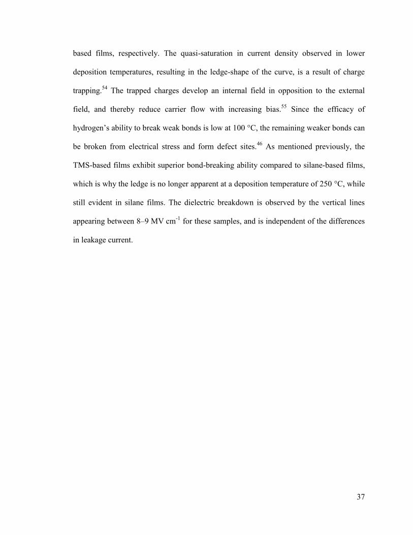
37
based films, respectively. The quasi-saturation in current density observed in lower
deposition temperatures, resulting in the ledge-shape of the curve, is a result of charge
trapping.54 The trapped charges develop an internal field in opposition to the external
field, and thereby reduce carrier flow with increasing bias.55 Since the efficacy of
hydrogen’s ability to break weak bonds is low at 100 °C, the remaining weaker bonds can
be broken from electrical stress and form defect sites.46 As mentioned previously, the
TMS-based films exhibit superior bond-breaking ability compared to silane-based films,
which is why the ledge is no longer apparent at a deposition temperature of 250 °C, while
still evident in silane films. The dielectric breakdown is observed by the vertical lines
appearing between 8–9 MV cm-1 for these samples, and is independent of the differences
in leakage current.
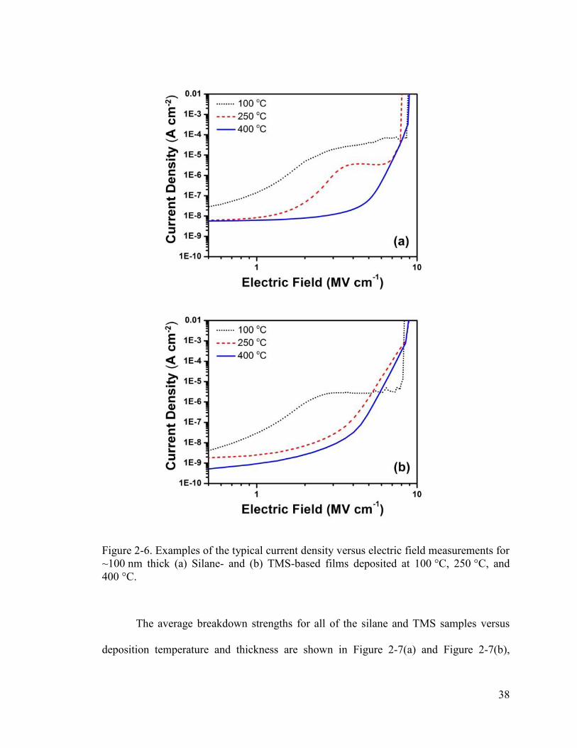
38
Figure 2-6. Examples of the typical current density versus electric field measurements for ~100 nm thick (a) Silane- and (b) TMS-based films deposited at 100 °C, 250 °C, and 400 °C.
The average breakdown strengths for all of the silane and TMS samples versus
deposition temperature and thickness are shown in Figure 2-7(a) and Figure 2-7(b),
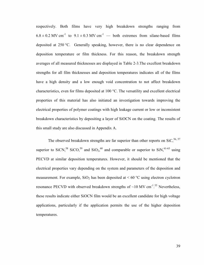
39
respectively. Both films have very high breakdown strengths ranging from
6.8 ± 0.2 MV cm-1 to 9.1 ± 0.3 MV cm-1 — both extremes from silane-based films
deposited at 250 °C. Generally speaking, however, there is no clear dependence on
deposition temperature or film thickness. For this reason, the breakdown strength
averages of all measured thicknesses are displayed in Table 2-3.The excellent breakdown
strengths for all film thicknesses and deposition temperatures indicates all of the films
have a high density and a low enough void concentration to not affect breakdown
characteristics, even for films deposited at 100 °C. The versatility and excellent electrical
properties of this material has also initiated an investigation towards improving the
electrical properties of polymer coatings with high leakage current or low or inconsistent
breakdown characteristics by depositing a layer of SiOCN on the coating. The results of
this small study are also discussed in Appendix A.
The observed breakdown strengths are far superior than other reports on SiC,56, 57
superior to SiCN,58 SiCO,59 and SiO2,60 and comparable or superior to SiN,61-63 using
PECVD at similar deposition temperatures. However, it should be mentioned that the
electrical properties vary depending on the system and parameters of the deposition and
measurement. For example, SiO2 has been deposited at < 60 °C using electron cyclotron
resonance PECVD with observed breakdown strengths of ~10 MV cm-1.55 Nevertheless,
these results indicate either SiOCN film would be an excellent candidate for high voltage
applications, particularly if the application permits the use of the higher deposition
temperatures.
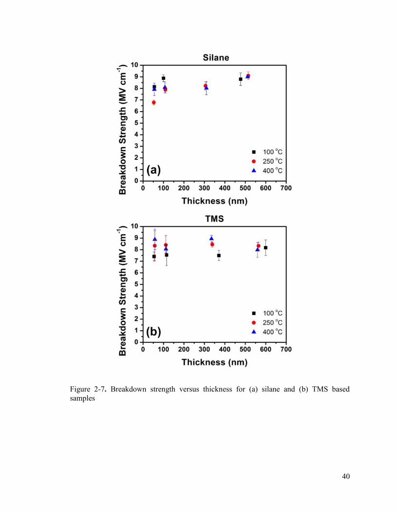
40
Figure 2-7. Breakdown strength versus thickness for (a) silane and (b) TMS based samples
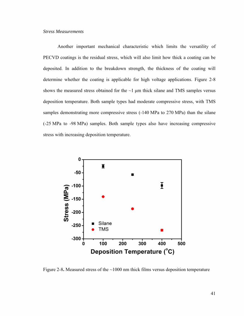
41
Stress Measurements
Another important mechanical characteristic which limits the versatility of
PECVD coatings is the residual stress, which will also limit how thick a coating can be
deposited. In addition to the breakdown strength, the thickness of the coating will
determine whether the coating is applicable for high voltage applications. Figure 2-8
shows the measured stress obtained for the ~1 μm thick silane and TMS samples versus
deposition temperature. Both sample types had moderate compressive stress, with TMS
samples demonstrating more compressive stress (-140 MPa to 270 MPa) than the silane
(-25 MPa to -98 MPa) samples. Both sample types also have increasing compressive
stress with increasing deposition temperature.
Figure 2-8. Measured stress of the ~1000 nm thick films versus deposition temperature
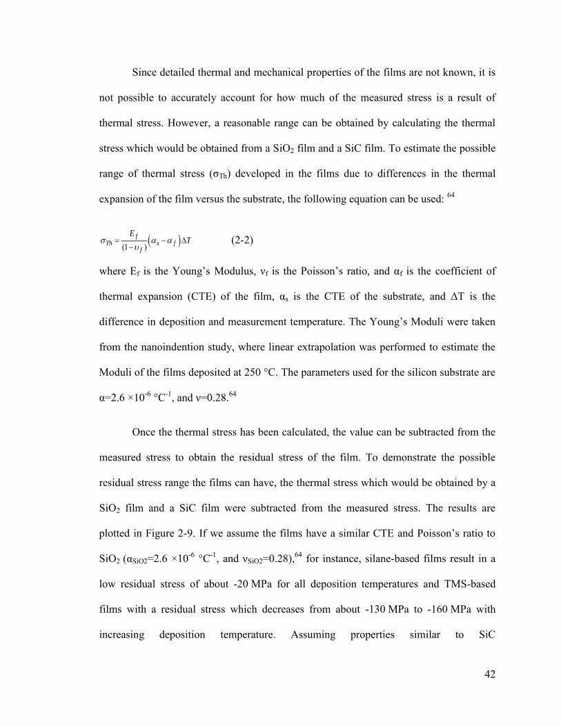
42
Since detailed thermal and mechanical properties of the films are not known, it is
not possible to accurately account for how much of the measured stress is a result of
thermal stress. However, a reasonable range can be obtained by calculating the thermal
stress which would be obtained from a SiO2 film and a SiC film. To estimate the possible
range of thermal stress (σTh) developed in the films due to differences in the thermal
expansion of the film versus the substrate, the following equation can be used: 64
(1 )f
Th s ff
ET
(2-2)
where Ef is the Young’s Modulus, νf is the Poisson’s ratio, and αf is the coefficient of
thermal expansion (CTE) of the film, αs is the CTE of the substrate, and ΔT is the
difference in deposition and measurement temperature. The Young’s Moduli were taken
from the nanoindention study, where linear extrapolation was performed to estimate the
Moduli of the films deposited at 250 °C. The parameters used for the silicon substrate are
α=2.6 ×10⁻⁶ °C-1, and ν=0.28.64
Once the thermal stress has been calculated, the value can be subtracted from the
measured stress to obtain the residual stress of the film. To demonstrate the possible
residual stress range the films can have, the thermal stress which would be obtained by a
SiO2 film and a SiC film were subtracted from the measured stress. The results are
plotted in Figure 2-9. If we assume the films have a similar CTE and Poisson’s ratio to
SiO2 (αSiO2=2.6 ×10⁻⁶ °C-1, and νSiO2=0.28),64 for instance, silane-based films result in a
low residual stress of about -20 MPa for all deposition temperatures and TMS-based
films with a residual stress which decreases from about -130 MPa to -160 MPa with
increasing deposition temperature. Assuming properties similar to SiC
43
(αSiC=2.6×10⁻⁶ °C-1, and νSiC=0.28),64 however, shift the residual stress to more
compressive values, due to the higher CTE of SiC. It is interesting to note that silane-
based SiOCN films have been grown thicker than 30 μm without delamination or signs of
fracture. TMS based films, on the other hand, start showing signs of failure after a few
μm. Therefore, we can assume that at least the silane-based films have similar thermal
and mechanical properties to SiO2, because low stress is required to achieve such thick
films. In addition, since the increasing compressive stress due to increasing deposition
temperature is mostly accounted for with this assumption in properties (i.e. the stress
values are more consistent across the deposition temperatures), the thermal stress is likely
a major contributor for the decrease in stress from increasing temperature.
Figure 2-9. Measured stress and the residual stress calculated by subtracting the theoretical thermal stress developed between Si and SiO2 or SiC.
44
Many studies have observed that higher hydrogen concentrations within thin films
grown by PECVD result in films with more compressive stress.65, 66 This, however, does
not explain the more compressive nature of the TMS-based films compared to silane-
based films, or the more compressive nature of films at higher deposition temperatures,
because FTIR results clearly indicate lower concentrations of hydrogen-containing
moieties. With a higher concentration of Si–C bonds, we might expect the TMS-based
films to behave more like SiC, which has a higher CTE than Si (as compared to SiO2 with
a lower CTE) and should consequently result in more tensile stress. Therefore, we
speculate the additional compressive stress to be caused by other, more complicated
effects from the differences in the internal structure. For instance, it could be an effect of
increased density as seen from the AFM images and the lower Si–O–Si stretching
frequency from FTIR,64 or differences in the bonding configurations within the films.67
However, further investigation is needed to provide a more detailed explanation.
Etch Resistance
Both types of SiOCN have proven to be extremely resistant to many wet etchants
indicating it can be used as a masking material within MEMs fabrication processes, such
as those required of the fabrication of thin film capacitors. For example, concentrated
hydrofluoric acid (37% v/v) in ethanol (1:1 by volume) results in etch rates of roughly
15 nm min-1 and 1 nm min-1 for silane and TMS based SiOCN deposited at 400 °C,
respectively. Silane based SiOCN (400 °C) has also shown a slow etch rate of about 1.3
nm min-1 in phosphoric acid (@ 180 °C) and no discernible etching after 30 min in strong
45
oxidizers such as Aqua Regia (3 HCl : 1 HNO3 @ 75 °C), or Cyantek CR-9 (ceric
ammonium nitrate solution).
2.4 Conclusions
The characterizations of two types of SiOCN films grown by PECVD have been
presented. The results suggest the properties of the silane-based SiOCN films render it a
better candidate for the fabrication of multilayer capacitors discussed in Chapter 3.
Silane-based films can be grown to large thicknesses, owing to its low residual stress.
Large thicknesses and high breakdown strengths of > 7 MV cm-1 are properties useful for
high voltage applications. The low average surface roughness of <0.7 nm and suggested
high density of the material is also advantageous for thin film capacitors in the prevention
of electric field enhancements observed at propagating points or from internal voids, as
mentioned in Chapter 1. Finally, the etch resistance against a number of different etchants
renders it a good candidate as a masking material within devices fabricated using
standard microelectronic techniques.
46
2.5 References
1. Grill, A., Plasma enhanced chemical vapor deposited SiCOH dielectrics: from low-k to extreme low-k interconnect materials. J. Appl. Phys. 2003, 93, 1785-1790.
2. Grill, A.; Patel, V., Low dielectric constant films prepared by plasma-enhanced chemical vapor deposition from tetramethylsilane. J. Appl. Phys. 1999, 85, 3314-3318.
3. Kim, C. Y.; Kim, S. H.; Navamathavan, R.; Choi, C. K.; Jeung, W. Y., Characteristics of low-k SiOC(–H) films deposited at various substrate temperature by PECVD using DMDMS/O2 precursor. Thin Solid Films 2007, 516, 340-344.
4. Alayo, M. I.; Pereyra, I.; Scopel, W. L.; Fantini, M. C. A., On the nitrogen and oxygen incorporation in plasma-enhanced chemical vapor deposition (PECVD) SiOxNy films. Thin Solid Films 2002, 402, 154-161.
5. Matsuda, Y.; King, S. W.; Dauskardt, R. H., Tailored amorphous silicon carbide barrier dielectrics by nitrogen and oxygen doping. Thin Solid Films 2013, 531, 552-558.
6. Mandracci, P.; Ricciardi, C., Silicon–carbon–oxynitrides grown by plasma-enhanced chemical vapor deposition technique. Thin Solid Films 2007, 515, 7639-7642.
7. Zhou, Y.; Probst, D.; Thissen, A.; Kroke, E.; Riedel, R.; Hauser, R.; Hoche, H.; Broszeit, E.; Kroll, P.; Stafast, H., Hard silicon carbonitride films obtained by RF-plasma-enhanced chemical vapour deposition using the single-source precursor bis (trimethylsilyl) carbodiimide. J. Eur. Ceram. Soc. 2006, 26, 1325-1335.
8. Zhou, Y.; Yan, X.; Kroke, E.; Riedel, R.; Probst, D.; Thissen, A.; Hauser, R.; Ahles, M.; Von Seggern, H., Deposition Temperature Effect on the Structure and Optical Property of RF‐PACVD‐Derived Hydrogenated SiCNO Film. Materialwiss.
Werkstofftech. 2006, 37, 173-177.
9. Zhou, Y.; Probst, D.; Thissen, A.; Kroke, E.; Riedel, R.; Hauser, R.; Hoche, H.; Broszeit, E.; Kroll, P.; Stafast, H., Hard silicon carbonitride films obtained by RF-plasma-enhanced chemical vapour deposition using the single-source precursor bis(trimethylsilyl)carbodiimide. J. Eur. Ceram. Soc. 2006, 26, 1325-1335.
10. Grill, A.; Sternhagen, V.; Neumayer, D.; Patel, V., Hydrogen plasma effects on ultralow-k porous SiCOH dielectrics. J. Appl. Phys. 2005, 98, 074502.
47
11. Pan, P.; Nesbit, L. A.; Douse, R. W.; Gleason, R. T., The Composition and Properties of PECVD Silicon Oxide Films. J. Electrochem. Soc. 1985, 132, 2012-2019.
12. Kim, H.-S.; Gilmer, D. C.; Campbell, S. A.; Polla, D. L., Leakage current and electrical breakdown in metal-organic chemical vapor deposited TiO[sub 2] dielectrics on silicon substrates. Appl. Phys. Lett. 1996, 69, 3860-3862.
13. Demichelis, F.; Crovini, G.; Pirri, C.; Tresso, E.; Galloni, R.; Rizzoli, R.; Summonte, C.; Zignani, F.; Rava, P.; Madan, A., The influence of hydrogen dilution on the optoelectronic and structural properties of hydrogenated amorphous silicon carbide films. Philos. Mag. B 1994, 69, 377-386.
14. Street, R., Model for growth of a-Si: H and its alloys. Physical Review B 1991, 44, 10610.
15. Ganguly, G.; Matsuda, A., Defect formation during growth of hydrogenated amorphous silicon. Physical Review B 1993, 47, 3661.
16. Rajagopalan, T.; Wang, X.; Lahlouh, B.; Ramkumar, C.; Dutta, P.; Gangopadhyay, S., Low temperature deposition of nanocrystalline silicon carbide films by plasma enhanced chemical vapor deposition and their structural and optical characterization. J. Appl. Phys. 2003, 94, 5252-5260.
17. Hu, Z.; Liao, X.; Diao, H.; Kong, G.; Zeng, X.; Xu, Y., Amorphous silicon carbide films prepared by H2 diluted silane–methane plasma. J. Cryst. Growth 2004, 264, 7-12.
18. Zhang, H.; Xu, Z., Microstructure of nanocrystalline SiC films deposited by modified plasma-enhanced chemical vapor deposition. Opt. Mater. 2002, 20, 177-181.
19. Rocheleau, R. E.; Zhang, Z.; Niles, D. W.; Mason, A., Effect of hydrogen dilution on the properties and bonding in plasma‐deposited silicon nitride. J. Appl. Phys. 1992, 72, 282-284.
20. Stapinski, T.; Ambrosone, G.; Coscia, U.; Giorgis, F.; Pirri, C. F., Defect characterization of a-SiC:H and a-SiN:H alloys produced by ultrahigh vacuum plasma enhanced chemical vapor deposition in different plasma conditions. Physica B:
Condensed Matter 1998, 254, 99-106.
48
21. Middya, A.; Ray, S.; Jones, S.; Williamson, D., Improvement of microstructure of amorphous silicon–germanium alloys by hydrogen dilution. J. Appl. Phys. 1995, 78, 4966-4974.
22. Wu, J.-J.; Chen, K.-H.; Wen, C.-Y.; Chen, L.-C.; Wang, J.-K.; Yu, Y.-C.; Wang, C.-W.; Lin, E.-K., Effect of H2 addition on SiCN film growth in an electron cyclotron resonance plasma chemical vapor deposition reactor. J. Mater. Chem. 2000, 10, 783-787.
23. Gangopadhyay, S.; Hossain, M.; Gangapadhyay, K. NANOCOMPOSITE DIELECTRIC COATINGS. 2009.
24. Ishizaka, A.; Shiraki, Y., Low Temperature Surface Cleaning of Silicon and Its Application to Silicon MBE. J. Electrochem. Soc. 1986, 133, 666-671.
25. Choi, K.; Harris, H.; Gangopadhyay, S.; Temkin, H., Cleaning of Si and properties of the HfO2–Si interface. J. Vac. Sci. Tech., A 2003, 21, 718-722.
26. Stoney, G. G., The Tension of Metallic Films Deposited by Electrolysis. Proceedings of the Royal Society of London. Series A, Containing Papers of a
Mathematical and Physical Character 1909, 82, 172-175.
27. Hopcroft, M. A.; Nix, W. D.; Kenny, T. W., What is the Young's Modulus of Silicon? J. Microelectromech. Syst. 2010, 19, 229-238.
28. Wortman, J.; Evans, R., Young's modulus, shear modulus, and Poisson's ratio in silicon and germanium. J. Appl. Phys. 1965, 36, 153.
29. Darwent, B., Bond dissociation energies in simple molecules. NSRDS-NBS NO.
31, U. S. DEPT. COMMERCE, WASHINGTON, D. C. JAN. 1970, 48 P 1970.
30. Dupuis, J.; Fourmond, E.; Ballutaud, D.; Bererd, N.; Lemiti, M., Optical and structural properties of silicon oxynitride deposited by plasma enhanced chemical vapor deposition. Thin Solid Films 2010, 519, 1325-1333.
31. Grill, A.; Neumayer, D. A., Structure of low dielectric constant to extreme low dielectric constant SiCOH films: Fourier transform infrared spectroscopy characterization. J. Appl. Phys. 2003, 94, 6697-6707.
49
32. Sassella, A.; Borghesi, A.; Corni, F.; Monelli, A.; Ottaviani, G.; Tonini, R.; Pivac, B.; Bacchetta, M.; Zanotti, L., Infrared study of Si-rich silicon oxide films deposited by plasma-enhanced chemical vapor deposition. Journal of Vacuum Science & Technology
A 1997, 15, 377-389.
33. Ay, F.; Aydinli, A., Comparative investigation of hydrogen bonding in silicon based PECVD grown dielectrics for optical waveguides. Opt. Mater. 2004, 26, 33-46.
34. Karakuscu, A.; Guider, R.; Pavesi, L.; Soraru, G. D., White Luminescence from Sol–Gel‐Derived SiOC Thin Films. J. Am. Ceram. Soc. 2009, 92, 2969-2974.
35. Cao, Z., Plasma enhanced deposition of silicon carbonitride thin films and property characterization. Diamond Relat. Mater. 2002, 11, 16-21.
36. Wrobel, A.; Błaszczyk, I.; Walkiewicz-Pietrzykowska, A.; Tracz, A.; Klemberg-Sapieha, J.; Aoki, T.; Hatanaka, Y., Remote hydrogen–nitrogen plasma chemical vapor deposition from a tetramethyldisilazane source. Part 1. Mechanism of the process, structure and surface morphology of deposited amorphous hydrogenated silicon carbonitride films. J. Mater. Chem. 2003, 13, 731-737.
37. Ogata, K.; Chubaci, J. F. D.; Fujimoto, F., Properties of carbon nitride films with composition ratio C/N= 0.5–3.0 prepared by the ion and vapor deposition method. J.
Appl. Phys. 1994, 76, 3791-3796.
38. Claassen, W.; vd Pol, H. T.; Goemans, A.; Kuiper, A., Characterization of Silicon‐Oxynitride Films Deposited by Plasma‐Enhanced CVD. J. Electrochem. Soc.
1986, 133, 1458-1464.
39. Theil, J.; Tsu, D.; Watkins, M.; Kim, S.; Lucovsky, G., Local bonding environments of Si–OH groups in SiO2 deposited by remote plasma-enhanced chemical vapor deposition and incorporated by postdeposition exposure to water vapor. J. Vac. Sci.
Tech., A 1990, 8, 1374-1381.
40. Lucovsky, G.; Tsu, D. V., Plasma enhanced chemical vapor deposition: Differences between direct and remote plasma excitation. J. Vac. Sci. Tech., A 1987, 5, 2231-2238.
41. Blaszczyk-Lezak, I.; Wrobel, A.; Kivitorma, M.; Vayrynen, I.; Tracz, A., Silicon carbonitride by remote microwave plasma CVD from organosilicon precursor: Growth
50
mechanism and structure of resulting Si: C: N films. Appl. Surf. Sci. 2007, 253, 7211-7218.
42. Peter, S.; Bernütz, S.; Berg, S.; Richter, F., FTIR analysis of a-SiCN:H films deposited by PECVD. Vacuum 2013, 98, 81-87.
43. Lucovsky, G.; Mantini, M.; Srivastava, J.; Irene, E., Low‐temperature growth of silicon dioxide films: A study of chemical bonding by ellipsometry and infrared spectroscopy. J. Vac. Sci. Tech., B 1987, 5, 530-537.
44. Pryce Lewis, H. G.; Edell, D. J.; Gleason, K. K., Pulsed-PECVD films from hexamethylcyclotrisiloxane for use as insulating biomaterials. Chem. Mater. 2000, 12, 3488-3494.
45. Venables, J.; Spiller, G.; Hanbucken, M., Nucleation and growth of thin films. Rep. Prog. Phys. 1984, 47, 399.
46. Street, R., Hydrogen diffusion and electronic metastability in amorphous silicon. Physica B: Condensed Matter 1991, 170, 69-81.
47. Pham, H. T.; Akkaya, T.; de Boer, C.; Visser, C.; Sarro, P. In Electrical and
Optical Properties of PECVD SiC Thin Film for Surface Micromachined Devices, Proceedings of SeSens 2002-Workshop on Semiconductor Sensors, Citeseer: 2002.
48. Patrick, W. J.; Schwartz, G. C.; Chapple‐Sokol, J. D.; Carruthers, R.; Olsen, K., Plasma‐Enhanced Chemical Vapor Deposition of Silicon Dioxide Films Using Tetraethoxysilane and Oxygen: Characterization and Properties of Films. J. Electrochem.
Soc. 1992, 139, 2604-2613.
49. Lim, S. W.; Shimogaki, Y.; Nakano, Y.; Tada, K.; Komiyama, H., Reduction Mechanism in the Dielectric Constant of Fluorine‐Doped Silicon Dioxide Film. J.
Electrochem. Soc. 1997, 144, 2531-2537.
50. Robertson, J.; Powell, M. J., Deposition, defect and weak bond formation processes in a-Si:H. Thin Solid Films 1999, 337, 32-36.
51. Srivastava, J.; Prasad, M.; Wagner, J., Electrical conductivity of silicon dioxide thermally grown on silicon. J. Electrochem. Soc. 1985, 132, 955-963.
51
52. Dorda, G.; Vrba, J., Electrical conductivity of silicon oxide. Surf. Sci. 1967, 6, 369-376.
53. Lorenz, H.; Eisele, I.; Ramm, J.; Edlinger, J.; Bühler, M., Characterization of low temperature SiO2 and Si3N4 films deposited by plasma enhanced evaporation. J. Vac.
Sci. Tech., B 1991, 9, 208-214.
54. Jeon, Y. C.; Lee, H. Y.; Joo, S. K., I‐V characteristics of electron‐cyclotron‐resonance plasma‐enhanced chemical‐vapor‐deposition silicon nitride thin films. J. Appl. Phys. 1994, 75, 979-984.
55. Isai, G. I.; Holleman, J.; Wallinga, H.; Woerlee, P. H., Conduction and trapping mechanisms in SiO 2 films grown near room temperature by multipolar electron cyclotron resonance plasma enhanced chemical vapor deposition. J. Vac. Sci. Tech., B:
Microelectronics and nanometer structures 2004, 22, 1022-1029.
56. Brassard, D.; El Khakani, M. A., Dielectric properties of amorphous hydrogenated silicon carbide thin films grown by plasma-enhanced chemical vapor deposition. J. Appl. Phys. 2003, 93, 4066-4071.
57. Tsui, B.-Y.; Kuo-Lung, F.; Shyh-Dar, L., Electrical instability of low-dielectric constant diffusion barrier film (a-SiC:H) for copper interconnect. Electron Devices, IEEE
Transactions on 2001, 48, 2375-2383.
58. Peter, S.; Günther, M.; Berg, S.; Clausner, A.; Richter, F., Mid-frequency PECVD of a-SiCN:H films and their structural, mechanical and electrical properties. Vacuum
2013, 90, 155-159.
59. Grill, A.; Patel, V., Ultralow-k dielectrics prepared by plasma-enhanced chemical vapor deposition. Appl. Phys. Lett. 2001, 79, 803-805.
60. Haque, M.; Naseem, H.; Brown, W., Characterization of high rate deposited PECVD silicon dioxide films for MCM applications. J. Electrochem. Soc. 1995, 142, 3864-3869.
61. Herth, E.; Legrand, B.; Buchaillot, L.; Rolland, N.; Lasri, T., Optimization of SiNX: H films deposited by PECVD for reliability of electronic, microsystems and optical applications. Microelectronics Reliability 2010, 50, 1103-1106.
52
62. Piccirillo, A.; Gobbi, A., Physical‐Electrical Properties of Silicon Nitride Deposited by PECVD on III–V Semiconductors. J. Electrochem. Soc. 1990, 137, 3910-3917.
63. Parsons, G. N.; Souk, J. H.; Batey, J., Low hydrogen content stoichiometric silicon nitride films deposited by plasma‐enhanced chemical vapor deposition. J. Appl.
Phys. 1991, 70, 1553-1560.
64. Tarraf, A.; Daleiden, J.; Irmer, S.; Prasai, D.; Hillmer, H., Stress investigation of PECVD dielectric layers for advanced optical MEMS. Journal of micromechanics and
microengineering 2004, 14, 317.
65. El Khakani, M.; Chaker, M.; Jean, A.; Boily, S.; Pépin, H.; Kieffer, J.; Gujrathi, S., Effect of rapid thermal annealing on both the stress and the bonding states of a‐SiC: H films. J. Appl. Phys. 1993, 74, 2834-2840.
66. Hughey, M. P.; Cook, R. F., Stress development kinetics in plasma-enhanced chemical-vapor-deposited silicon nitride films. J. Appl. Phys. 2005, 97, 114914.
67. Gunde, M. K.; Maček, M., The relationship between the macroscopic properties of PECVD silicon nitride and oxynitride layers and the characteristics of their networks. Appl. Phys. A 2002, 74, 181-186.
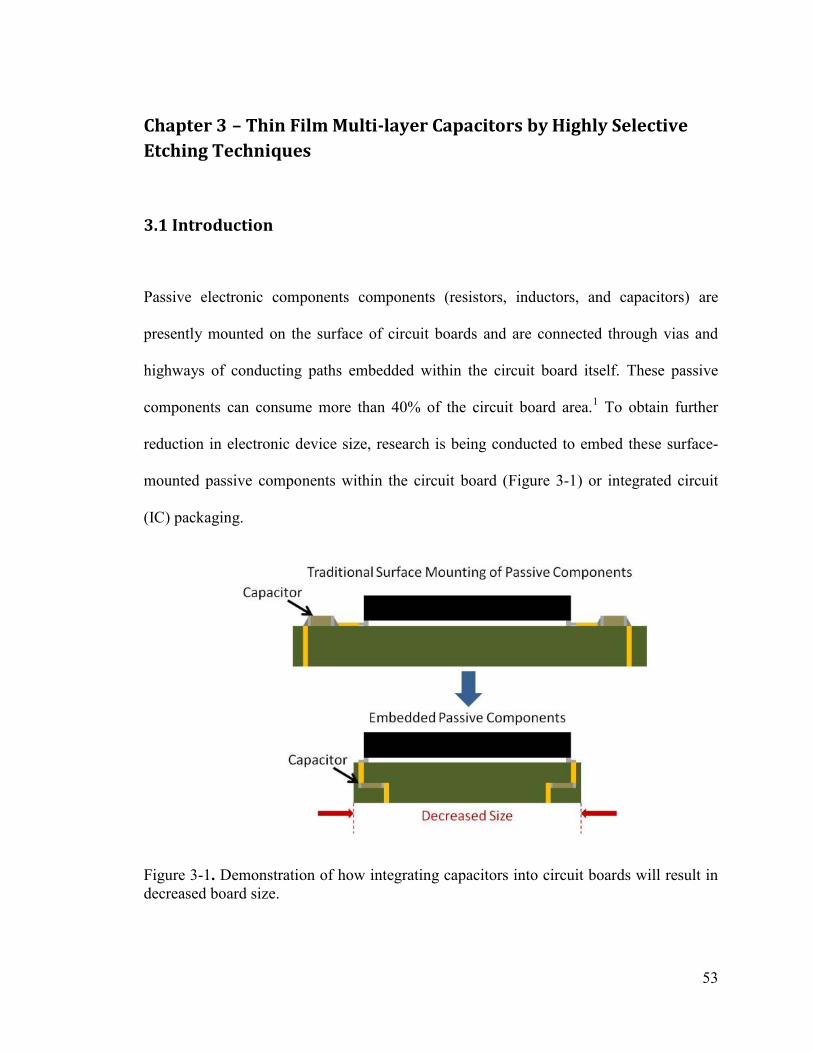
53
Chapter 3 – Thin Film Multi-layer Capacitors by Highly Selective
Etching Techniques
3.1 Introduction
Passive electronic components components (resistors, inductors, and capacitors) are
presently mounted on the surface of circuit boards and are connected through vias and
highways of conducting paths embedded within the circuit board itself. These passive
components can consume more than 40% of the circuit board area.1 To obtain further
reduction in electronic device size, research is being conducted to embed these surface-
mounted passive components within the circuit board (Figure 3-1) or integrated circuit
(IC) packaging.
Figure 3-1. Demonstration of how integrating capacitors into circuit boards will result in decreased board size.
54
As touched on in Chapter 1, thin film deposition techniques promise to be the
future of the miniaturization of passive component development, due to the ability to
deposit uniform, dense, and smooth dielectric and metal layers, which are all factors
which can significantly affect the performance and reliability of the current multilayer
capacitor technology.2 However, many of the recently reported thin film multilayer
capacitor fabrication methods are disadvantageous in that the electrode layers are
connected through a series of vias.3, 4 Therefore, the fabrication process is very
cumbersome and adds a significant number of processing steps, increasing the probability
of device failure and the overall cost of the device, as well as wasting valuable footprint
area. In an attempt to overcome this issue, Imamiya et al.5 demonstrated multilayer
capacitors fabricated by magnetron sputtering through successive shadow masks to
outline the features of alternating platinum electrodes and the barium titanate dielectric.
However, shadow masks require smooth surfaces, can pose as a substrate or device
scratching hazard, and the masking capabilities are not sufficient for CVD or atomic layer
deposition processes.
To achieve a multilayer capacitor process which is more scalable, efficient,
universal and can be deposited from a variety of deposition systems, a process which
does not require a separate patterning step for each layer is needed. Such fabrication
processes have previously been visualized and patented in which two different electrode
materials with highly selective etchants are alternated throughout the multilayer
capacitor. 6, 7 The concept is to make the full mulitlayer stack first, and only two or three
patterning steps are needed to connect alternate electrode layers and create a capacitor
with an arbitrary number of layers. However, these ideas have not been realized in the
55
market today. The key to the success of this method is finding two electrode materials
with isotropic etching processes which are extremely selective to only that material, and
do not attack the other electrode material of the dielectric. Additionally, the electrode
material would ideally have a high conductivity to reduce loss due to equivalent series
resistances.
To this end, we have developed a process utilizing highly selective etching of two
metals, platinum (Pt) and ruthenium (Ru), to significantly decrease the processing steps
required in fabricating thin film multilayer capacitors. The current process was developed
as a proof-of-concept approach in which the investigated dielectric layer (silicon
oxycarbonitride) was deposited by plasma-enhanced chemical vapor depsoition
(PECVD), and the metal layers were deposited using sputtering. The advantage of this
process is that all of the layers are deposited sequentially, followed by the same top-down
fabrication process regardless of the number of layers. This process could therefore be
easily transferable to single systems or cluster tools to deposit all of the layers in situ,
which would reduce the chance for defects or atmospheric contamination.
3.2 Materials and Methods
Deposition of Layers
Silicon (Si) wafers were used as the substrate for these devices. The Si substrates
were cleaved into large pieces, typically ~2 inches × 6 inches, and then rinsed in acetone,
methanol, and isopropyl alcohol, sonicated in an acetone bath for 10 minutes, and placed
56
in a dilute HF bath followed by rinsing in DI water and subsequent drying under blowing
nitrogen.
A PECVD grown Silicon oxycarbonitride (SiOCN) was chosen as the dielectric
for the fabrication of the devices, the deposition parameters of which are described in
Chapter 2. In short, silane (15 sccm), methane (150 sccm), nitrous oxide (300 sccm), and
hydrogen (1800 sccm) were introduced into an Applied Materials Precision 5000 PECVD
deposition chamber at a pressure of 7 Torr, RF power of 400 W, and substrate
temperature of 400 °C. As previously discussed, silane-based SiOCN was chosen because
of the good electrical properties, low residual stress, ability to deposit very thick films,
and observed excellent chemical resistance to all of the etchants used throughout the
process. This material was chosen for fabrication proof-of-concept, and it should be
mentioned that other materials will also be suitable for this process. In fact, SiO2 and
HfO2 also show excellent etch resistance to the Ru and Pt etchants.
The Ru and Pt electrodes were deposited using a magnetron sputter deposition
system (AJA International, Inc.). Both metals were sputter deposited to ~30 nm using a
2 in. target (Kurt J. Lesker) at 200 W RF power, chamber pressure of 4 mTorr, argon
flow rate of 20 sccm, and target-to-substrate distance of 6 inches. Titanium (~5 nm) was
deposited before and after the Pt electrode for adhesion, but for simplification of the
process description we will refer to this Ti/Pt/Ti layer as solely a Pt layer. Chromium (Cr)
was sputtered for use as a dry etching mask and the sidewall electrode, and was also
sputtered using the same conditions as above except with a 3 inch target and 200 W DC
power.
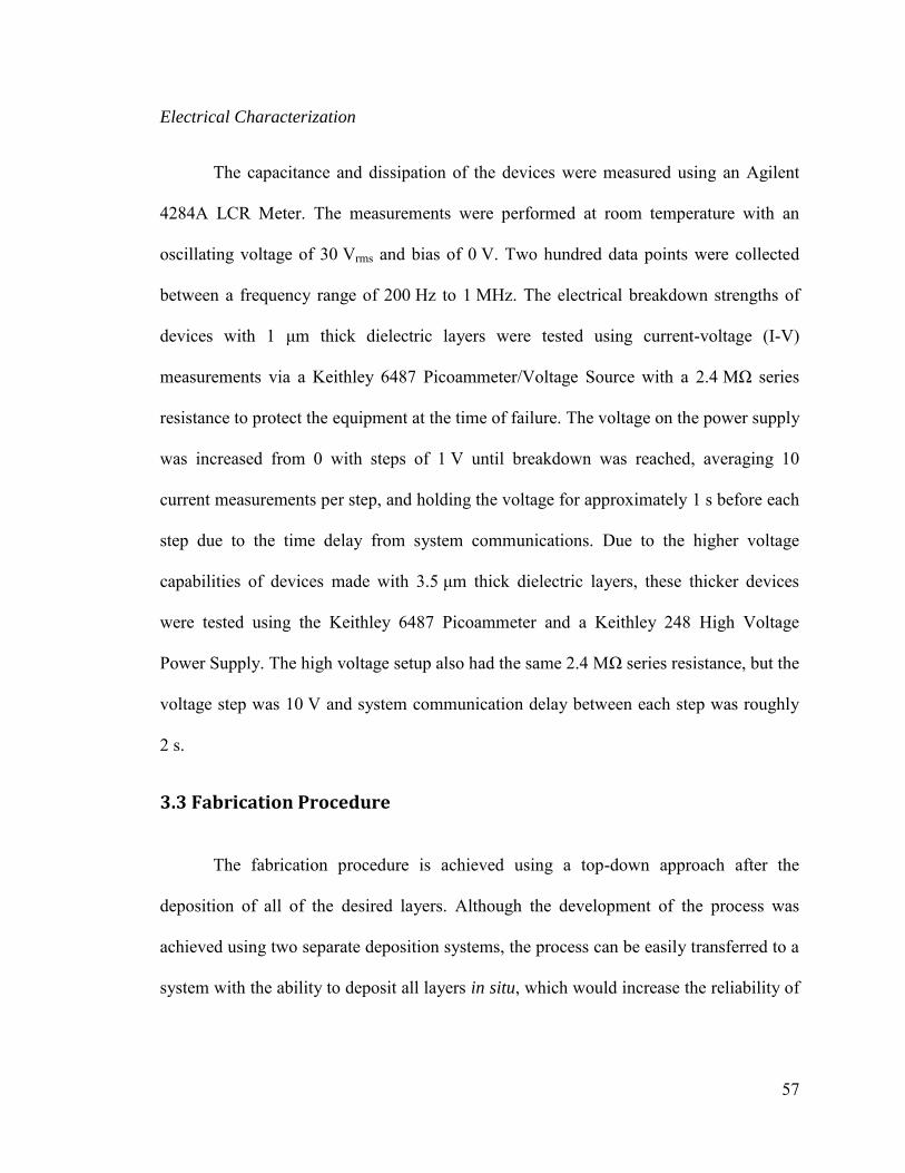
57
Electrical Characterization
The capacitance and dissipation of the devices were measured using an Agilent
4284A LCR Meter. The measurements were performed at room temperature with an
oscillating voltage of 30 Vrms and bias of 0 V. Two hundred data points were collected
between a frequency range of 200 Hz to 1 MHz. The electrical breakdown strengths of
devices with 1 μm thick dielectric layers were tested using current-voltage (I-V)
measurements via a Keithley 6487 Picoammeter/Voltage Source with a 2.4 MΩ series
resistance to protect the equipment at the time of failure. The voltage on the power supply
was increased from 0 with steps of 1 V until breakdown was reached, averaging 10
current measurements per step, and holding the voltage for approximately 1 s before each
step due to the time delay from system communications. Due to the higher voltage
capabilities of devices made with 3.5 μm thick dielectric layers, these thicker devices
were tested using the Keithley 6487 Picoammeter and a Keithley 248 High Voltage
Power Supply. The high voltage setup also had the same 2.4 MΩ series resistance, but the
voltage step was 10 V and system communication delay between each step was roughly
2 s.
3.3 Fabrication Procedure
The fabrication procedure is achieved using a top-down approach after the
deposition of all of the desired layers. Although the development of the process was
achieved using two separate deposition systems, the process can be easily transferred to a
system with the ability to deposit all layers in situ, which would increase the reliability of
58
the process and decrease the probability of defects. Figure 3-2 illustrates a simplified
fabrication process flow, with a detailed description provided below.
Figure 3-2. Thin film multi-layer capacitor fabrication process for a two-layer device. A short description of the process as is follows: (a) deposit all layers alternating Pt and Ru electrodes until desired number of layers is achieved and pattern devices with Cr hard mask, (b) dry etch to define device area, (c) remove Cr mask, expose one side of devices using photolithography and selectively etch Ru, (d) deposit Cr sidewall to connect all exposed Ru electrodes, (e) expose opposite side using photolithography and selectively undercut Pt, (f) deposit another Cr sidewall to connect all exposed Pt electrodes to complete the devices. An elaborated process description is provided in the text. Illustration not drawn to scale.
The following steps were followed to deposit all of the layers to achieve the
structure illustrated in Figure 3-2(a) prior to device fabrication: i) SiOCN was first
deposited as an insulating layer on the Si substrate, ii) a Pt layer was deposited as the first
electrode, iii) SiOCN was deposited again to a thickness of either 1 μm or 3.5 μm to test
the changes in electrical properties from different dielectric thicknesses, iv) a Ru layer
was deposited as the second electrode, v) SiOCN was deposited again to the same
thickness as Step iii, and vi) the process was repeated from Step ii until the desired
59
number of layers had been reached. The device finishes with a SiOCN deposition because
this is also necessary for electrical insulation when the sidewall electrodes are deposited
to connect alternate electrodes. We will refer to the devices tested within this work as
one-, two-, or three-layer devices, which correspond to the number of active capacitive
layers (e.g. a two-layer device consists of a Si substrate-
SiOCN/Pt/SiOCN/Ru/SiOCN/Pt/SiOCN stack).
After deposition of all the layers was completed, a ~800 nm thick Cr mask was
then sputtered and patterned on the stack into 2.5 mm x 2.5 mm squares using standard
photolithography techniques. Cr was chosen as the mask material as it exhibited superior
etching protection compared to photoresist or aluminum. All photolithography steps
throughout the fabrication process were performed using Futurexx NR5-8000 negative
photoresist, which was selected owing to its adequate etch resistance for the wet etch
processing. The photoresist was removed using Futurexx RR-41 resist remover solution
at a temperature of ~60 °C.
The devices were etched out of the layers using magnetically-enhanced reactive
ion etching using the Applied Materials Precision 5000 etching chamber, resulting in
devices similar to that displayed in Figure 3-2(b). The etching recipes corresponding and
etch rates are displayed in Table 3-1. The devices were etched down to at least 300 nm
into the bottom-most insulating SiOCN layer to ensure the bottom-most electrode was
well exposed. The SiOCN etching was cycled between the ‘Dielectric Etch’ for 5 min,
followed by a 60 s delay, a 10 s ‘Cr Etch,’ another 60 s delay, and repeating until the
metal layer was exposed. The ‘Cr Etch’ step was found to significantly improve the
etching uniformity and resulting roughness, which is believed to have been caused by Cr
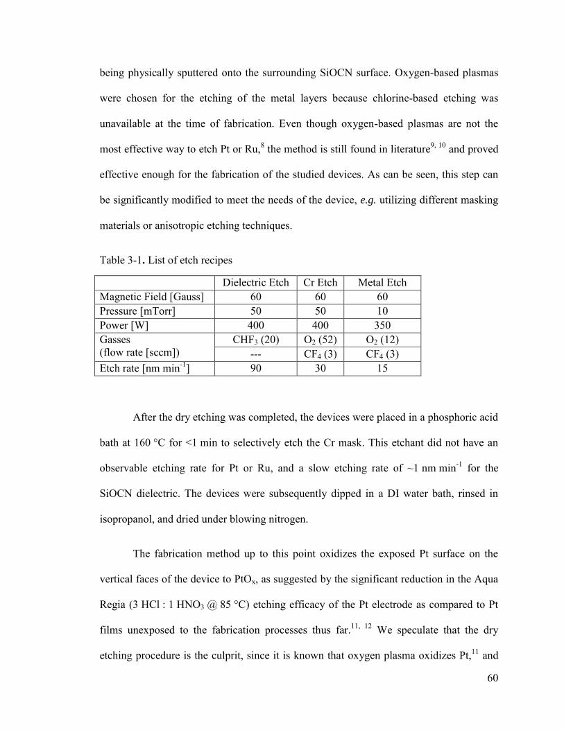
60
being physically sputtered onto the surrounding SiOCN surface. Oxygen-based plasmas
were chosen for the etching of the metal layers because chlorine-based etching was
unavailable at the time of fabrication. Even though oxygen-based plasmas are not the
most effective way to etch Pt or Ru,8 the method is still found in literature9, 10 and proved
effective enough for the fabrication of the studied devices. As can be seen, this step can
be significantly modified to meet the needs of the device, e.g. utilizing different masking
materials or anisotropic etching techniques.
Table 3-1. List of etch recipes
Dielectric Etch Cr Etch Metal Etch Magnetic Field [Gauss] 60 60 60 Pressure [mTorr] 50 50 10 Power [W] 400 400 350 Gasses (flow rate [sccm])
CHF3 (20) O2 (52) O2 (12) --- CF4 (3) CF4 (3)
Etch rate [nm min-1] 90 30 15
After the dry etching was completed, the devices were placed in a phosphoric acid
bath at 160 °C for <1 min to selectively etch the Cr mask. This etchant did not have an
observable etching rate for Pt or Ru, and a slow etching rate of ~1 nm min-1 for the
SiOCN dielectric. The devices were subsequently dipped in a DI water bath, rinsed in
isopropanol, and dried under blowing nitrogen.
The fabrication method up to this point oxidizes the exposed Pt surface on the
vertical faces of the device to PtOx, as suggested by the significant reduction in the Aqua
Regia (3 HCl : 1 HNO3 @ 85 °C) etching efficacy of the Pt electrode as compared to Pt
films unexposed to the fabrication processes thus far.11, 12 We speculate that the dry
etching procedure is the culprit, since it is known that oxygen plasma oxidizes Pt,11 and
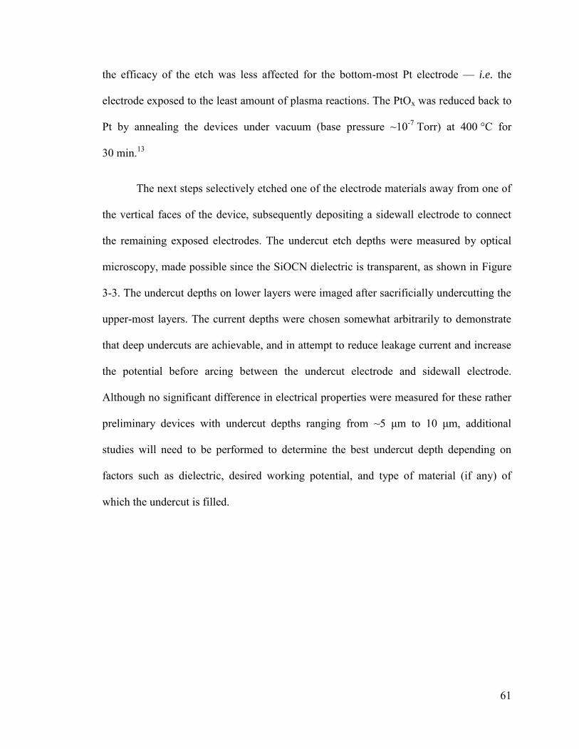
61
the efficacy of the etch was less affected for the bottom-most Pt electrode — i.e. the
electrode exposed to the least amount of plasma reactions. The PtOx was reduced back to
Pt by annealing the devices under vacuum (base pressure ~10-7 Torr) at 400 °C for
30 min.13
The next steps selectively etched one of the electrode materials away from one of
the vertical faces of the device, subsequently depositing a sidewall electrode to connect
the remaining exposed electrodes. The undercut etch depths were measured by optical
microscopy, made possible since the SiOCN dielectric is transparent, as shown in Figure
3-3. The undercut depths on lower layers were imaged after sacrificially undercutting the
upper-most layers. The current depths were chosen somewhat arbitrarily to demonstrate
that deep undercuts are achievable, and in attempt to reduce leakage current and increase
the potential before arcing between the undercut electrode and sidewall electrode.
Although no significant difference in electrical properties were measured for these rather
preliminary devices with undercut depths ranging from ~5 μm to 10 μm, additional
studies will need to be performed to determine the best undercut depth depending on
factors such as dielectric, desired working potential, and type of material (if any) of
which the undercut is filled.
62
Figure 3-3. Optical microscopy image of the device showing (a) before and (b) after a Ru undercut etching.
Photolithography was used again to expose only one side of the device. The
window in the photoresist had dimensions of 0.7 mm × 2.9 mm, and was placed so that it
overlapped with the device by approximately 0.2 mm, as illustrated in Figure 3-4(a). The
samples were subsequently placed in a Cyantek CR-9 etchant at 35 °C under slight
agitation for 10 min to selectively etch the Ru electrode about 8–10 μm away from the
edge of the structure. Performing the etch at room temperature for 30 min only undercuts
the Ru about 5 μm, after which point the etch rate was significantly hindered, probably a
result of the long diffusion lengths of the reactants and products, as well as the formation
of bubbles. The former process was utilized for the devices with 1μm thick dielectric
layers, while the latter process was used during the formation of the devices with 3.5 μm
63
thick dielectric layers. This etching step had no measurable Pt or SiOCN removal,
resulting in only the Pt electrodes remaining exposed on the face of the device, as
observed in Figure 3-2(c). The devices were rinsed in DI water followed by a 90 s O2
plasma (100 sccm O2, 250 mTorr, 100W RF, 60 Gauss) to clean the surface, which was
found to improve Cr adhesion to SiOCN after the Ru etching step. The devices were
subsequently placed within the sputter tool, where Cr was deposited as the sidewall
electrode material to connect all exposed Pt electrodes, followed by lift-off. The devices
were then as shown in Figure 3-2(d). Sputter deposition was chosen to deposit the
sidewall electrode since sputtering results in more uniform coverage over sidewalls than
evaporation techniques. The Cr sidewall electrode was deposited to thicknesses ranging
from 300 nm to 750 nm as measured on a flat substrate. The various thicknesses were
investigated because the Cr was originally intended to be used as a mask as well as
electrode during the Aqua Regia etching step, since the etch rate was observed to be a
low ~1 nm min-1. Despite this low etch rate, it was anomalously discovered that the Cr
itself provided no significant masking capability. During the etching step, the electrical
contact between the Pt and Cr was lost, therefore requiring the use of another photoresist
mask for the Pt etch. No significant differences were observed in the investigated
electrical characteristics between the different Cr sidewall thicknesses.
Photolithography was performed one last time to expose only the opposite side of
the device using the same method as that in the Ru selective etching step. The devices
were left undisturbed at ambient conditions for at least one hour after developing the
photoresist. This step was discovered to be necessary to ensure the photoresist did not
delaminate or crack during the Aqua Regia etching step. After 30 min of etching under
64
slight agitation, the Pt layers were undercut about 5-10 μm away from the edge of the
device. The large range in undercut depth is a result of irregular reproducibility across
devices and etching attempts, warranting further investigation towards improvement.
Again, this selective etching step had no measurable Ru or SiOCN removal, resulting in
only the Ru electrodes remaining exposed on this face of the device (Figure 3-2(e)). It
should be mentioned that the Aqua Regia reacts with the NR5-8000 photoresist, but the
masking is adequate within the investigated etching time for proper device fabrication.
The reacted photoresist was removed with the resist remover and the devices were re-
patterned exposing the same area, followed by another O2 plasma. To complete the
devices (Figure 3-2(f)), a Cr sidewall was deposited to make contact between all Ru
electrodes followed by lift-off.
3.4 Results and Discussion
A photograph of six completed devices is presented in Figure 3-4(b). Figure
3-4(c) shows a SEM image of a one-layer completed device with 1 μm SiOCN dielectric
layers. The image demonstrates the undercut Pt layer and confirms the contact between
the Ru layer and Cr sidewall electrode.
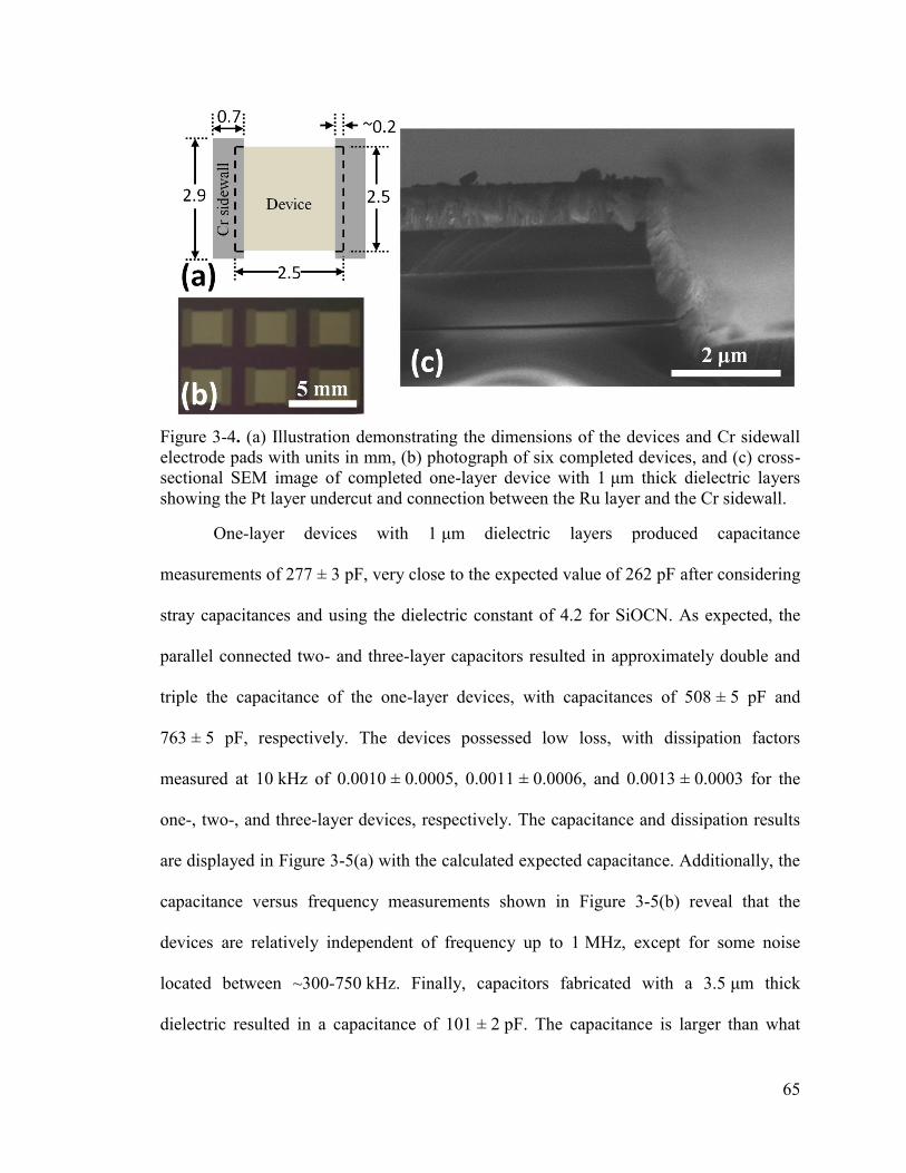
65
Figure 3-4. (a) Illustration demonstrating the dimensions of the devices and Cr sidewall electrode pads with units in mm, (b) photograph of six completed devices, and (c) cross-sectional SEM image of completed one-layer device with 1 μm thick dielectric layers showing the Pt layer undercut and connection between the Ru layer and the Cr sidewall.
One-layer devices with 1 μm dielectric layers produced capacitance
measurements of 277 ± 3 pF, very close to the expected value of 262 pF after considering
stray capacitances and using the dielectric constant of 4.2 for SiOCN. As expected, the
parallel connected two- and three-layer capacitors resulted in approximately double and
triple the capacitance of the one-layer devices, with capacitances of 508 ± 5 pF and
763 ± 5 pF, respectively. The devices possessed low loss, with dissipation factors
measured at 10 kHz of 0.0010 ± 0.0005, 0.0011 ± 0.0006, and 0.0013 ± 0.0003 for the
one-, two-, and three-layer devices, respectively. The capacitance and dissipation results
are displayed in Figure 3-5(a) with the calculated expected capacitance. Additionally, the
capacitance versus frequency measurements shown in Figure 3-5(b) reveal that the
devices are relatively independent of frequency up to 1 MHz, except for some noise
located between ~300-750 kHz. Finally, capacitors fabricated with a 3.5 μm thick
dielectric resulted in a capacitance of 101 ± 2 pF. The capacitance is larger than what
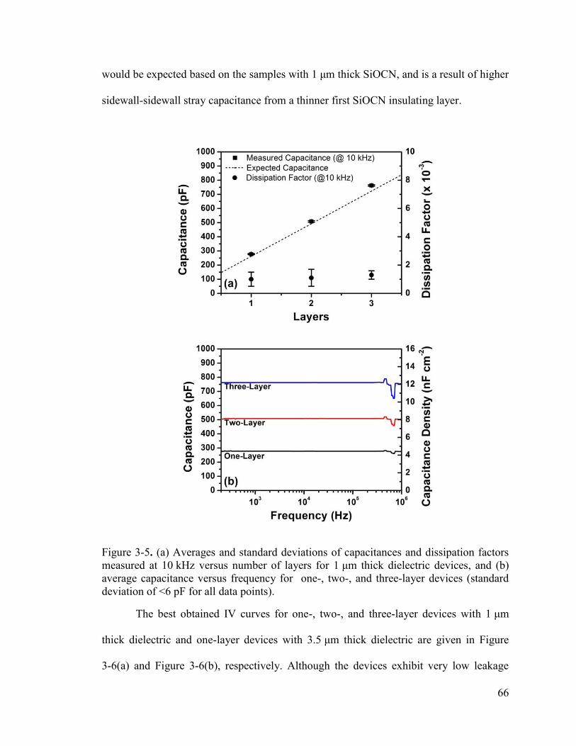
66
would be expected based on the samples with 1 μm thick SiOCN, and is a result of higher
sidewall-sidewall stray capacitance from a thinner first SiOCN insulating layer.
Figure 3-5. (a) Averages and standard deviations of capacitances and dissipation factors measured at 10 kHz versus number of layers for 1 μm thick dielectric devices, and (b) average capacitance versus frequency for one-, two-, and three-layer devices (standard deviation of <6 pF for all data points).
The best obtained IV curves for one-, two-, and three-layer devices with 1 μm
thick dielectric and one-layer devices with 3.5 μm thick dielectric are given in Figure
3-6(a) and Figure 3-6(b), respectively. Although the devices exhibit very low leakage
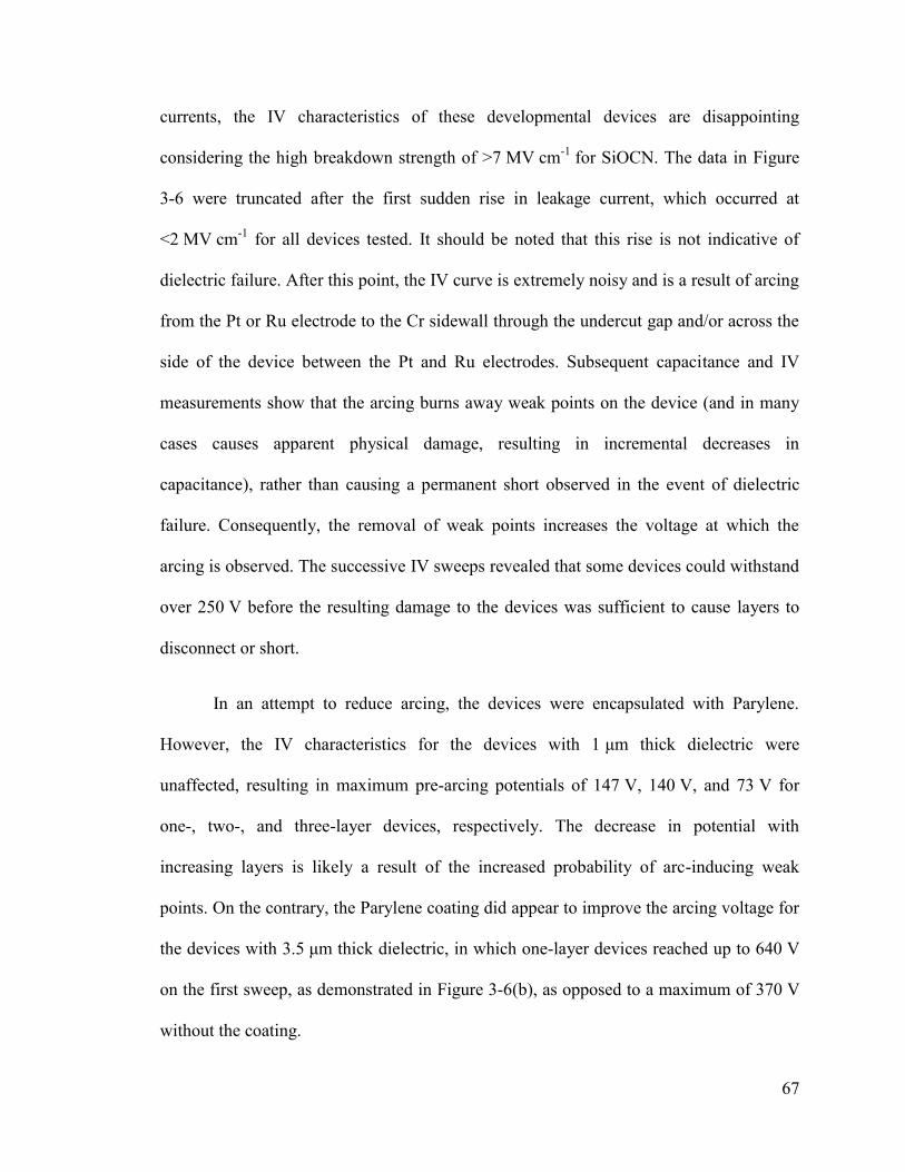
67
currents, the IV characteristics of these developmental devices are disappointing
considering the high breakdown strength of >7 MV cm-1 for SiOCN. The data in Figure
3-6 were truncated after the first sudden rise in leakage current, which occurred at
<2 MV cm-1 for all devices tested. It should be noted that this rise is not indicative of
dielectric failure. After this point, the IV curve is extremely noisy and is a result of arcing
from the Pt or Ru electrode to the Cr sidewall through the undercut gap and/or across the
side of the device between the Pt and Ru electrodes. Subsequent capacitance and IV
measurements show that the arcing burns away weak points on the device (and in many
cases causes apparent physical damage, resulting in incremental decreases in
capacitance), rather than causing a permanent short observed in the event of dielectric
failure. Consequently, the removal of weak points increases the voltage at which the
arcing is observed. The successive IV sweeps revealed that some devices could withstand
over 250 V before the resulting damage to the devices was sufficient to cause layers to
disconnect or short.
In an attempt to reduce arcing, the devices were encapsulated with Parylene.
However, the IV characteristics for the devices with 1 μm thick dielectric were
unaffected, resulting in maximum pre-arcing potentials of 147 V, 140 V, and 73 V for
one-, two-, and three-layer devices, respectively. The decrease in potential with
increasing layers is likely a result of the increased probability of arc-inducing weak
points. On the contrary, the Parylene coating did appear to improve the arcing voltage for
the devices with 3.5 μm thick dielectric, in which one-layer devices reached up to 640 V
on the first sweep, as demonstrated in Figure 3-6(b), as opposed to a maximum of 370 V
without the coating.
68
Figure 3-6. Best obtained current leakage measurements for (a) one-, two-, and three-layer devices with 1 μm thick dielectric layers, and (b) one-layer devices with 3.5 μm thick dielectric layers. Inset: Current density versus electric field, calculated from the area of the device (2.5 mm × 2.5 mm) and the corresponding dielectric thickness.
69
Although this work clearly demonstrates a relatively simple process for the
fabrication of multilayer capacitors, the IV characteristics demonstrate that much
improvement is needed to achieve device-readiness. Future work will consist of
developing a process to fill the undercut gap with a dielectric material as well as electric
field modeling to provide pathways towards improving the voltage capabilities.
Regardless, this work demonstrates a method to fabricate thin film multilayer capacitors,
which can potentially be deposited from wide variety of methods, including cluster tools,
sputter deposition, and atomic layer deposition (ALD). The transferability to ALD is
particularly desirable, as it permits the ability to incorporate the devices on three-
dimensional substrates with high aspect ratio surfaces, which has received considerable
attention recently.14-17
3.5 Conclusions Although further optimizations are required to achieve device-ready capacitors,
we have demonstrated the successful fabrication of multilayer capacitors using the same
number of steps independent of the number of layers. The resulting process is potentially
scalable to capacitors with tens or even hundreds of layers, and is a good candidate for
the potential integration of thin film capacitors into circuit boards or IC packaging.
Acknowledgments
This work was funded by the U.S. Office of Naval Research under contract number
N00014-11-C-0392
70
3.6 References
1. Jianwen, X.; Wong, C. P. In Effects of the low loss polymers on the dielectric
behavior of novel aluminum-filled high-k nano-composites, Advanced Packaging Materials: Processes, Properties and Interfaces, 2004. Proceedings. 9th International Symposium on, 2004; 2004; pp 158-170.
2. Samantaray, M. M.; Gurav, A.; Dickey, E. C.; Randall, C. A., Electrode Defects in Multilayer Capacitors Part I: Modeling the Effect of Electrode Roughness and Porosity on Electric Field Enhancement and Leakage Current. J. Am. Ceram. Soc. 2012, 95, 257-263.
3. Schaper, L. W.; Thomason, C., High Density Double and Triple Layer Tantalum Pentoxide Decoupling Capacitors. Components and Packaging Technologies, IEEE
Transactions on 2007, 30, 563-568.
4. Klootwijk, J. H.; Jinesh, K. B.; Dekkers, W.; Verhoeven, J. F.; Van Den Heuvel, F. C.; Kim, H. D.; Blin, D.; Verheijen, M. A.; Weemaes, R. G. R.; Kaiser, M.; Ruigrok, J.; Roozeboom, F., Ultrahigh Capacitance Density for Multiple ALD-Grown MIM Capacitor Stacks in 3-D Silicon. Electron Device Letters, IEEE 2008, 29, 740-742.
5. Imamiya, Y.; Yokokawa, R.; Kanno, I.; Kotera, H. In Multilayer thin-film
capacitors fabricated by radio-frequency magnetron sputtering, Applications of Ferroelectrics (ISAF/PFM), 2011 International Symposium on and 2011 International Symposium on Piezoresponse Force Microscopy and Nanoscale Phenomena in Polar Materials, IEEE: 2011; pp 1-4.
6. Tigelaar, H. L.; Riemenschneider, B. R., Fabricating a stacked capacitor. Google Patents: 1987.
7. Willer, J.; Wendt, H.; Reisinger, H., Method for manufacturing a multi-layer capacitor. Google Patents: 1994.
8. Hsu, C. C.; Coburn, J. W.; Graves, D. B., Etching of ruthenium coatings in O2- and Cl2-containing plasmas. Journal of Vacuum Science & Technology A 2006, 24, 1-8.
9. Chou, C. H.; Phillips, J., Platinum metal etching in a microwave oxygen plasma. J. Appl. Phys. 1990, 68, 2415-2423.
71
10. Shibano, T.; Nakamura, K.; Oomori, T., Platinum etching in Ar/O2 mixed gas plasma with a thin SiO2 etching mask. Journal of Vacuum Science & Technology A 1998, 16, 502-508.
11. Kim, M. J.; Gruenke, L. A.; Saia, R. J.; Cohen, S. S., Inhibition of acid etching of Pt by pre‐exposure to oxygen plasma. Appl. Phys. Lett. 1984, 44, 462-464.
12. Köllensperger, P.; Karl, W.; Ahmad, M.; Pike, W.; Green, M., Patterning of platinum (Pt) thin films by chemical wet etching in Aqua Regia. Journal of
micromechanics and microengineering 2012, 22, 067001.
13. Liu, C.-L.; Lee, Z.-Y.; Wu, T.-B.; Lung, S.-L.; Liu, R., Polarization Switching Characteristics of Pb (Zr0. 5Ti0. 5) O3 Thin Films Deposited on Vacuum-Annealed PtOx/Pt Electrode. Japanese journal of applied physics 2002, 41, 6054.
14. Detalle, M.; Barrenetxea, M.; Muller, P.; Potoms, G.; Phommahaxay, A.; Soussan, P.; Vaesen, K.; De Raedt, W., High density, low leakage Back-End 3D capacitors for mixed signals applications. Microelectron. Eng. 2010, 87, 2571-2576.
15. Banerjee, P.; Perez, I.; Henn-Lecordier, L.; Lee, S. B.; Rubloff, G. W., Nanotubular metal–insulator–metal capacitor arrays for energy storage. Nature
Nanotechnology 2009, 4, 292-296.
16. Banerjee, P.; Perez, I.; Henn-Lecordier, L.; Lee, S. B.; Rubloff, G. W., ALD based Metal-insulator-metal (MIM) Nanocapacitors for Energy Storage. ECS
Transactions 2009, 25, 345-353.
17. Nongaillard, M.; Lallemand, F.; Allard, B., Design for manufacturing of 3D capacitors. Microelectron. J. 2010, 41, 845-850.
72
Chapter 4 – Investigations into the Crystal Growth of Nanoparticles
Sputter-Deposited into Ionic Liquids
4.1 Introduction
Ionic liquids (ILs) are room temperature molten salts, in other words, liquids
consisting entirely of ions. ILs are typically composed of a large, asymmetric cation and
charge-delocalized anion, resulting in a fairly weak interionic interaction, and thereby,
low melting temperatures.
ILs are being investigated as superior alternative solvents or electrolytes for
numerous applications, such as EDLCs, owing to the significant number of desirable
properties, from high ionic conductivity, significant electrochemical windows, negligible
vapor pressure, high temperature stability, to application-specific tunability (e.g.
functionalizing ILs with amines for enhanced CO2 capture), among others.1-4 The
negligible vapor pressure of ILs has allowed the usage of novel, cleaner, methodologies
using physical vapor deposition techniques to form unique nano-materials. Direct
deposition of materials into IL allows development of nano-materials without external
structure-directing agents or byproducts formed by conventional wet chemistry
techniques. As these agents and byproducts lead to additional electrochemical reactions
increasing the complexity of analytes or the products, it is particularly desirable that they
are absent while studying native electrochemical properties of nano-materials,5, 6 which
will be expanded upon in the next chapter.
73
Torimoto et al. first reported sputter deposition of gold into ILs,7 and further
demonstrated the ability to form metal alloys,8 and metal oxides.9 Since then, deposition
of metal NPs in ILs by sputter deposition,10 thermal evaporation,11 or by laser ablation
deposition12 is an area of active research, resulting in emerging applications of NP-in-IL
systems ranging from utilizing the catalytic behavior of the formed Pd NPs to
incorporating the IL with deposited Ag NPs into a thin film for pronounced antimicrobial
properties.13, 14 Investigations into the formation of the NPs formed via physical vapor
deposition in ILs show the particles start off as atoms/small clusters and continuously
increase in size over hours to days.10 Such growth is modulated by the deposited material
concentration, ionic structure, viscosity, and the concentration of impurities.10, 11, 15
However, observations of NP-in-IL dispersions over longer temporal scales clearly show
pronounced NP instability.10, 15
The classical inverse relationship of viscosity and temperature for ILs infers the
thermal stability of NPs at low temperatures, due to a significant decrease in Brownian
motion of the particles.16-18 Here, the thermal stability is exploited by using low
temperatures to not only drastically retard the growth rate of NPs, but also provide long-
term storage options. This has opened new vistas for better resolved investigation of NP
size-dependent phenomena. Additionally, we characterized NP growth within the IL
system using UV–Vis and transmission electron microscopy (TEM) and provided
explanations toward the crystalline growth mechanisms of the resultant NPs from low-
energy sputter deposition. Although many ILs were studied in this work, a more detailed
analysis was performed on [emim][EtSO4] since this IL showed more significant
74
electrochemical enhancement after the incorporation of sputtered NPs, as will be
discussed in the next chapter.
4.2 Materials and Methods
Ionic Liquid
The ionic liquids used in the studies were purchased from vendors and included the
following: 1-ethyl-3-methylimidazolium bis(trifluoromethylsulfonyl)imide
([emim][Tf2N], Covalent Associates >99.5%), 1-ethyl-3-methylimidazolium ethyl sulfate
([emim][EtSO4], BASF >95%), 1-ethyl-3-methylimidazolium dicyanamide
([emim][DCA], BASF >98%), 1-butyl-1-methylpyrrolidinium
bis(trifluoromethylsulfonyl)imide ([Bmpy][Tf2N], Aldrich >98%), 1-Hexyl-3-
methylimidazolium tetrafluoroborate ([hmim][BF4], Aldrich >97%), 1-Hexyl-3-
methylimidazolium hexafluorophosphate ([hmim][PF6], Fluka >97%), and 1-Methyl-3-
octylimidazolium tetrafluoroborate ([omim][BF4], Aldrich >97%). The ILs were dried
over night at ~30 mTorr and 50 °C to remove water. The IL was subsequently placed
under 5 × 10⁻⁷ Torr for at least 6 h for further drying before testing and deposition.
Sputter Deposition
One half mL of the IL was spread over a clean silicon substrate to form a thin film within
a ~13 cm diameter area followed by introduction into the sputtering system (ATC 2000
V, AJA International Inc., N. Scituate, MA) as shown in Figure 4-1(a). Gold or silver was
deposited using a 2 inch target (99.99%, Kurt J. Lesker) at 30 W RF power using an Ar
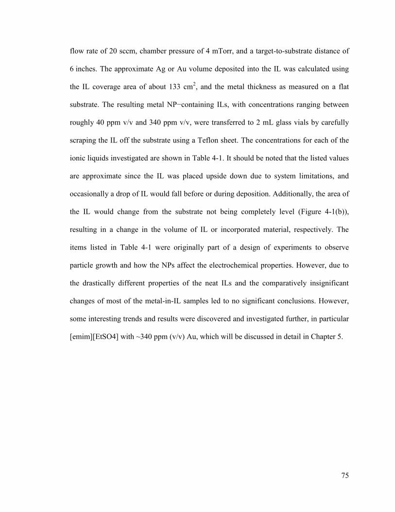
75
flow rate of 20 sccm, chamber pressure of 4 mTorr, and a target-to-substrate distance of
6 inches. The approximate Ag or Au volume deposited into the IL was calculated using
the IL coverage area of about 133 cm2, and the metal thickness as measured on a flat
substrate. The resulting metal NP−containing ILs, with concentrations ranging between
roughly 40 ppm v/v and 340 ppm v/v, were transferred to 2 mL glass vials by carefully
scraping the IL off the substrate using a Teflon sheet. The concentrations for each of the
ionic liquids investigated are shown in Table 4-1. It should be noted that the listed values
are approximate since the IL was placed upside down due to system limitations, and
occasionally a drop of IL would fall before or during deposition. Additionally, the area of
the IL would change from the substrate not being completely level (Figure 4-1(b)),
resulting in a change in the volume of IL or incorporated material, respectively. The
items listed in Table 4-1 were originally part of a design of experiments to observe
particle growth and how the NPs affect the electrochemical properties. However, due to
the drastically different properties of the neat ILs and the comparatively insignificant
changes of most of the metal-in-IL samples led to no significant conclusions. However,
some interesting trends and results were discovered and investigated further, in particular
[emim][EtSO4] with ~340 ppm (v/v) Au, which will be discussed in detail in Chapter 5.
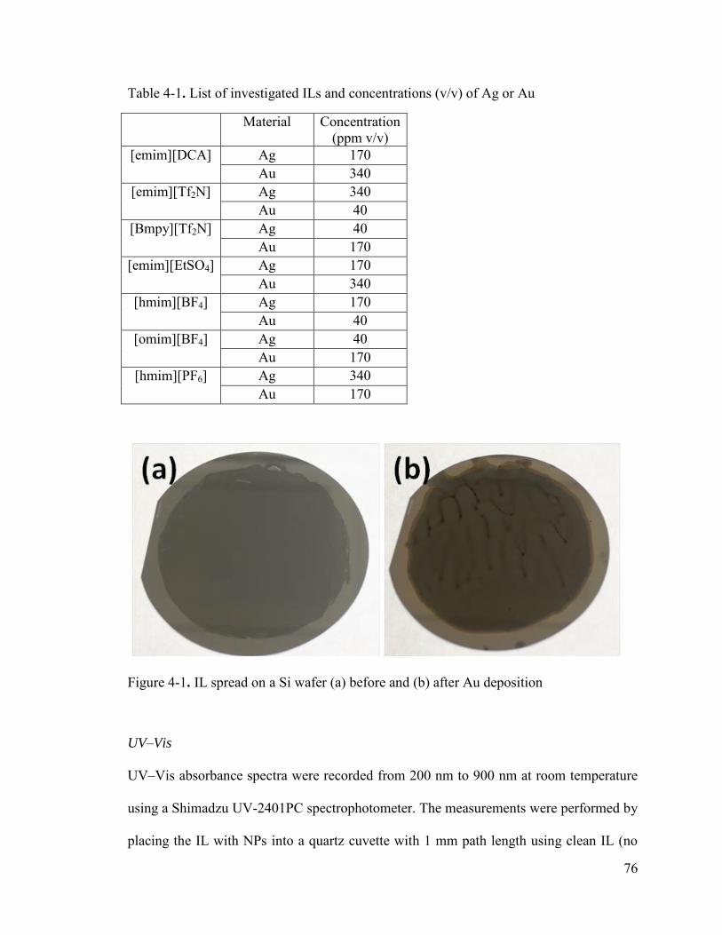
76
Table 4-1. List of investigated ILs and concentrations (v/v) of Ag or Au
Material
Concentration (ppm v/v)
[emim][DCA] Ag 170 Au 340
[emim][Tf2N] Ag 340 Au 40
[Bmpy][Tf2N] Ag 40 Au 170
[emim][EtSO4] Ag 170 Au 340
[hmim][BF4] Ag 170 Au 40
[omim][BF4] Ag 40 Au 170
[hmim][PF6] Ag 340 Au 170
Figure 4-1. IL spread on a Si wafer (a) before and (b) after Au deposition
UV–Vis
UV–Vis absorbance spectra were recorded from 200 nm to 900 nm at room temperature
using a Shimadzu UV-2401PC spectrophotometer. The measurements were performed by
placing the IL with NPs into a quartz cuvette with 1 mm path length using clean IL (no
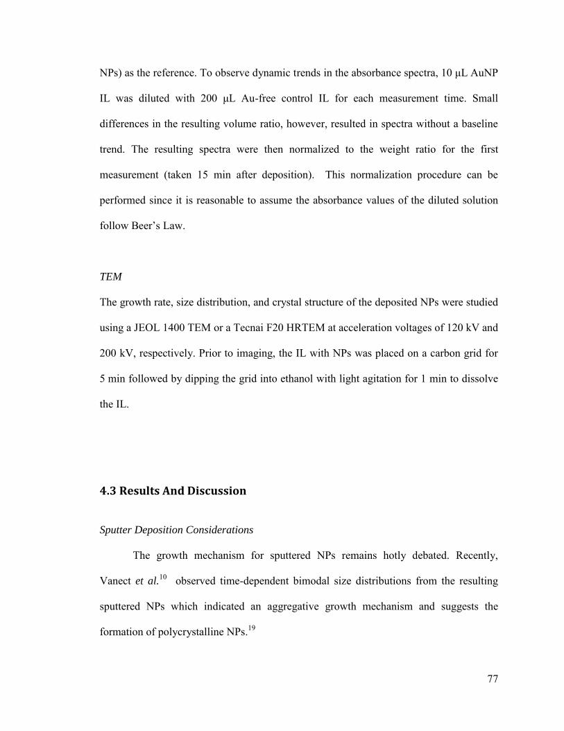
77
NPs) as the reference. To observe dynamic trends in the absorbance spectra, 10 μL AuNP
IL was diluted with 200 μL Au-free control IL for each measurement time. Small
differences in the resulting volume ratio, however, resulted in spectra without a baseline
trend. The resulting spectra were then normalized to the weight ratio for the first
measurement (taken 15 min after deposition). This normalization procedure can be
performed since it is reasonable to assume the absorbance values of the diluted solution
follow Beer’s Law.
TEM
The growth rate, size distribution, and crystal structure of the deposited NPs were studied
using a JEOL 1400 TEM or a Tecnai F20 HRTEM at acceleration voltages of 120 kV and
200 kV, respectively. Prior to imaging, the IL with NPs was placed on a carbon grid for
5 min followed by dipping the grid into ethanol with light agitation for 1 min to dissolve
the IL.
4.3 Results And Discussion
Sputter Deposition Considerations
The growth mechanism for sputtered NPs remains hotly debated. Recently,
Vanect et al.10 observed time-dependent bimodal size distributions from the resulting
sputtered NPs which indicated an aggregative growth mechanism and suggests the
formation of polycrystalline NPs.19
78
It is noteworthy that the growth process is a result of a number of different factors
including the deposition parameters as well as the IL composition, as will be discussed
later. Our group has recently shown the sputter deposition parameters are important to
control the energy of the deposited materials.20 A decrease in the mean-free path of
sputtered atoms/clusters due to high power (consisting of a higher atomic flux/deposition
rate) or deposition at high pressures, consequently increases the process of
thermalization. Thermalization of the sputtered atoms results in a reduction of
atom/cluster energy due to collisions and interactions with neighboring atoms/clusters
subsequently resulting in higher concentrations of larger atomic clusters being
incorporated into the IL.
Once the sputtered atoms/clusters enter the IL surface, Brownian motion within
the IL takes over. It is worth noting that Ag and AuNPs enter the IL surface with a slight
positive charge and thus are likely to attract anions to form a charge shielding layer.21
The effective root mean square Brownian velocity (ve) of particles within a liquid can be
given by the formula
3 be
e
k T
m (4-1)
where kb is the Boltzmann constant, T the temperature, and me is the effective particle
mass.22 In this case, me would include the mass of the particle with the additional mass of
the counter-ion sheath surrounding the NP. This assumption is made in accordance with
relatively strong interaction between the anions in the IL and metal. When the metal
atoms/clusters have a small effective mass, the Brownian dynamics are pronounced and
these metal atoms/clusters can move within the IL and due to high free energy (particle
free energy is inversely proportional the particle size), can fuse with other atoms or
79
clusters and form single crystal seeds which grow into single crystalline NPs. If during
sputtering the atoms/clusters undergo pronounced thermalization before entering the IL,
the average cluster size would be enhanced and the particle free energy from Brownian
dynamics of these clusters would be reduced. The result would be agglomerative growth
of nanoparticles and an absence of single crystal domains. The study performed by
Vanect et al.10 used a high deposition pressure of 75 mTorr which likely contributed to
the observed agglomerative growth for these reasons. Based on these assumptions, we
used low power, low gas pressure and thus low deposition rate for better control in
studying crystal growth.
UV–Vis
Immediately following the deposition, the resulting liquid is a dark brown (Figure
4-1(b)). UV–Vis absorbance spectra of diluted [emim][EtSO4] with 340 ppm v/v AuNP
with respect to time after deposition are plotted in Figure 4-2(a). The peak observed at
~510 nm is characteristic of the surface plasmon resonance (SPR) of AuNPs. A baseline
fit was then subtracted from the data to obtain peak position and absorbance from the
NPs while removing absorbance due to scattering as shown in Figure 4-2(b). The NPs
initially exhibit a low SPR absorbance peak because the sample consists of a large
fraction of sub-nanometer particles, which do not show the SPR behavior in the
investigated wavelength range.23 The corresponding peak position and peak absorbance
values from Figure 4-2(b) were then plotted in Figure 4-2(c) and Figure 4-2(d),
respectively. The peak position was found to shift towards higher wavelengths and the
80
peak absorbance increased with time, characteristic of particle growth which will be
discussed further in the following section.
Figure 4-2. (a) raw UV–Vis spectra of diluted [emim][EtSO4] with AuNPs at various times after deposition, (b) SPR peak growth with time, (c) peak wavelength position, and (d) peak absorbance values over time (data in (c) and (d) are taken from marked points in (b)). Results are normalized to the wt% of the first measurement.
TEM
Figure 4-3(a-c) shows examples of the obtained HRTEM images of [emim][EtSO4]
with 300 ppm v/v AuNP at 0.5 h, 7.5 h, and 43.3 h after deposition with the
corresponding size distribution histograms. The particle size of 1.3 ± 0.7 nm measured
only 0.5 h after deposition indicates that the atoms are able to move and form particles
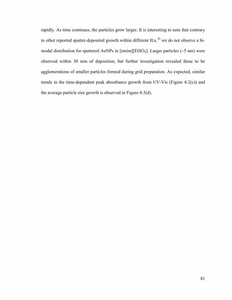
81
rapidly. As time continues, the particles grow larger. It is interesting to note that contrary
to other reported sputter-deposited growth within different ILs,10 we do not observe a bi-
modal distribution for sputtered AuNPs in [emim][EtSO4]. Larger particles (~5 nm) were
observed within 30 min of deposition, but further investigation revealed these to be
agglomerations of smaller particles formed during grid preparation. As expected, similar
trends in the time-dependent peak absorbance growth from UV-Vis (Figure 4-2(c)) and
the average particle size growth is observed in Figure 4-3(d).
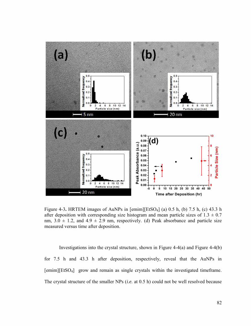
82
Figure 4-3. HRTEM images of AuNPs in [emim][EtSO4] (a) 0.5 h, (b) 7.5 h, (c) 43.3 h after deposition with corresponding size histogram and mean particle sizes of 1.3 ± 0.7 nm, 3.0 ± 1.2, and 4.9 ± 2.9 nm, respectively. (d) Peak absorbance and particle size measured versus time after deposition.
Investigations into the crystal structure, shown in Figure 4-4(a) and Figure 4-4(b)
for 7.5 h and 43.3 h after deposition, respectively, reveal that the AuNPs in
[emim][EtSO4] grow and remain as single crystals within the investigated timeframe.
The crystal structure of the smaller NPs (i.e. at 0.5 h) could not be well resolved because
83
IL which was not dissolved completely made focusing on the particles difficult. The
obtained HRTEM images confirmed nearly equidimentional FCC AuNPs.
Examples of TEM images of other ionic liquids and metals are shown in Figure
4-5. Here, we observed some ionic liquids with BF4–, PF6
–, and DCA– anions which
tended to promote particle coalescence and formed large particles or dendritic structures
([hmim][BF4] with AuNPs) over longer investigated time periods. Ionic liquids with
[Tf2N]– and [EtSO4] – anions, on the other hand, formed regions of accumulated 5-10 nm
Au or Ag particles which were separated by thin layers of ionic liquid, thereby preventing
coalescence. Table 4-2 provides a generalization of the resulting particle sizes, where ‘L’
denotes that large particles were typically formed, and ‘S’ denotes that the particles
remained small and separated. It should be noted that all samples contained some fraction
of large and small particles, but the notations are given to describe which trend was
observed more frequently.
These general trends suggest that the interaction between the anion and the metal
plays a significant role in particle growth. It should be noted that [Tf2N]– and [EtSO4]–
have more pronounced negatively charged regions which suggests higher interaction
energy with the highly electronegative Au surface than charge distributed anions such as
[BF4]– and [PF6]–,24, 25 for example. Additionally, the anions would have lower interaction
energy with the less electronegative Ag surface, suggesting Ag would be less stable.
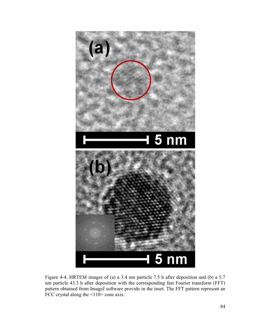
84
Figure 4-4. HRTEM images of (a) a 3.4 nm particle 7.5 h after deposition and (b) a 5.7 nm particle 43.3 h after deposition with the corresponding fast Fourier transform (FFT) pattern obtained from ImageJ software provide in the inset. The FFT pattern represent an FCC crystal along the <110> zone axis.
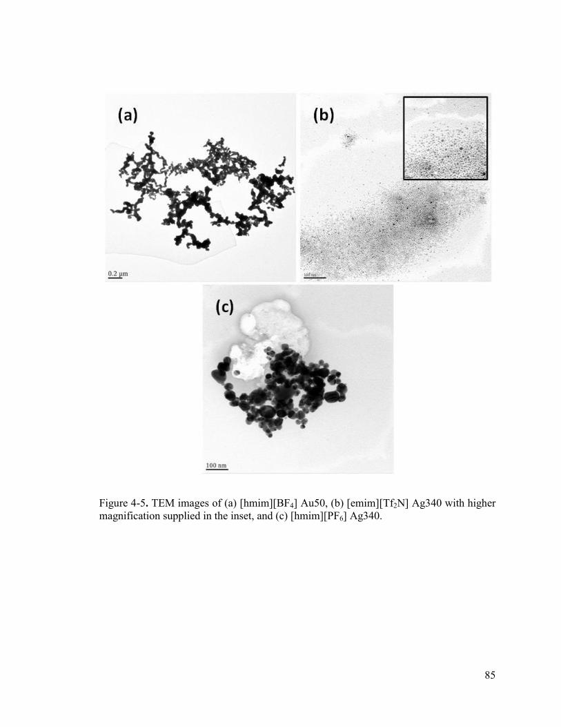
85
Figure 4-5. TEM images of (a) [hmim][BF4] Au50, (b) [emim][Tf2N] Ag340 with higher magnification supplied in the inset, and (c) [hmim][PF6] Ag340.
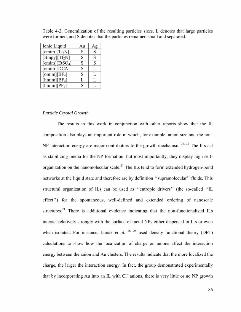
86
Table 4-2. Generalization of the resulting particles sizes. L denotes that large particles were formed, and S denotes that the particles remained small and separated.
Ionic Liquid Au Ag [emim][Tf2N] S S [Bmpy][Tf2N] S S [emim][EtSO4] S S [emim][DCA] S L [omim][BF4] S L [hmim][BF4] L L [hmim][PF6] S L
Particle Crystal Growth
The results in this work in conjunction with other reports show that the IL
composition also plays an important role in which, for example, anion size and the ion–
NP interaction energy are major contributors to the growth mechanism.26, 27 The ILs act
as stabilizing media for the NP formation, but most importantly, they display high self-
organization on the nanomolecular scale.21 The ILs tend to form extended hydrogen-bond
networks at the liquid state and therefore are by definition ‘‘supramolecular’’ fluids. This
structural organization of ILs can be used as ‘‘entropic drivers’’ (the so-called ‘‘IL
effect’’) for the spontaneous, well-defined and extended ordering of nanoscale
structures.21 There is additional evidence indicating that the non-functionalized ILs
interact relatively strongly with the surface of metal NPs either dispersed in ILs or even
when isolated. For instance, Janiak et al. 26, 28 used density functional theory (DFT)
calculations to show how the localization of charge on anions affect the interaction
energy between the anion and Au clusters. The results indicate that the more localized the
charge, the larger the interaction energy. In fact, the group demonstrated experimentally
that by incorporating Au into an IL with Cl– anions, there is very little or no NP growth
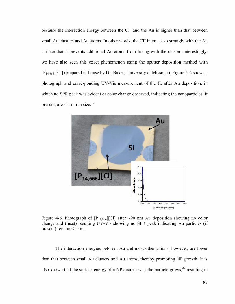
87
because the interaction energy between the Cl– and the Au is higher than that between
small Au clusters and Au atoms. In other words, the Cl– interacts so strongly with the Au
surface that it prevents additional Au atoms from fusing with the cluster. Interestingly,
we have also seen this exact phenomenon using the sputter deposition method with
[P14,666][Cl] (prepared in-house by Dr. Baker, University of Missouri). Figure 4-6 shows a
photograph and corresponding UV-Vis measurement of the IL after Au deposition, in
which no SPR peak was evident or color change observed, indicating the nanoparticles, if
present, are < 1 nm in size.19
Figure 4-6. Photograph of [P14,666][Cl] after ~90 nm Au deposition showing no color change and (inset) resulting UV-Vis showing no SPR peak indicating Au particles (if present) remain <1 nm.
The interaction energies between Au and most other anions, however, are lower
than that between small Au clusters and Au atoms, thereby promoting NP growth. It is
also known that the surface energy of a NP decreases as the particle grows,29 resulting in
88
decreased ion–NP interaction energy. Therefore, it is likely the ions act as a barrier to
prevent agglomeration yet still promote single crystal growth until a critical size is
reached, at which point agglomeration and polycrystalline growth takes effect.
Figure 4-7 illustrates a schematic demonstrating the developed theory for crystal
growth mechanisms for metal nanoparticles in ionic liquid. The process is described as
follows: (A) High concentrations of single atoms are initially deposited into the liquid
where (B) they collide and form small clusters or crystal seeds; (i) sufficiently high
interaction energy between the anion and the Au cluster (e.g. [P14,666][Cl]) prevents
further growth; (ii) interaction energy which is high enough to prevent clusters from
fusing (i.e the IL acts as a barrier between clusters), yet low enough to permit single
atoms, will promote single crystal growth; (iii) low interaction energy renders the IL
ineffective as a barrier against cluster agglomeration and coalescence, promoting
polycrystalline nanoparticles. As mentioned, it is possible the interaction energy will be
low enough after a critical crystal size has been achieved to promote agglomeration and
the formation of polycrystalline particles of the larger crystals, as well. It should also be
noted that although it is expected that the interaction energies would be different for other
materials, we expect the trends described in this theory to remain applicable.
In support of the provided theory, Watanabe et al.30 have reported the use of the
Derjaguin–Landua–Verwey–Overbeek (DLVO) theory to approximate the attractive
energy versus distance between nanoparticles in ILs and observed local energy
minimums with anion–dependent energy barrier heights. From this, we can speculate that
for the nanoparticles formed with [Tf2N]– and [EtSO4] – anions for example, the energy is
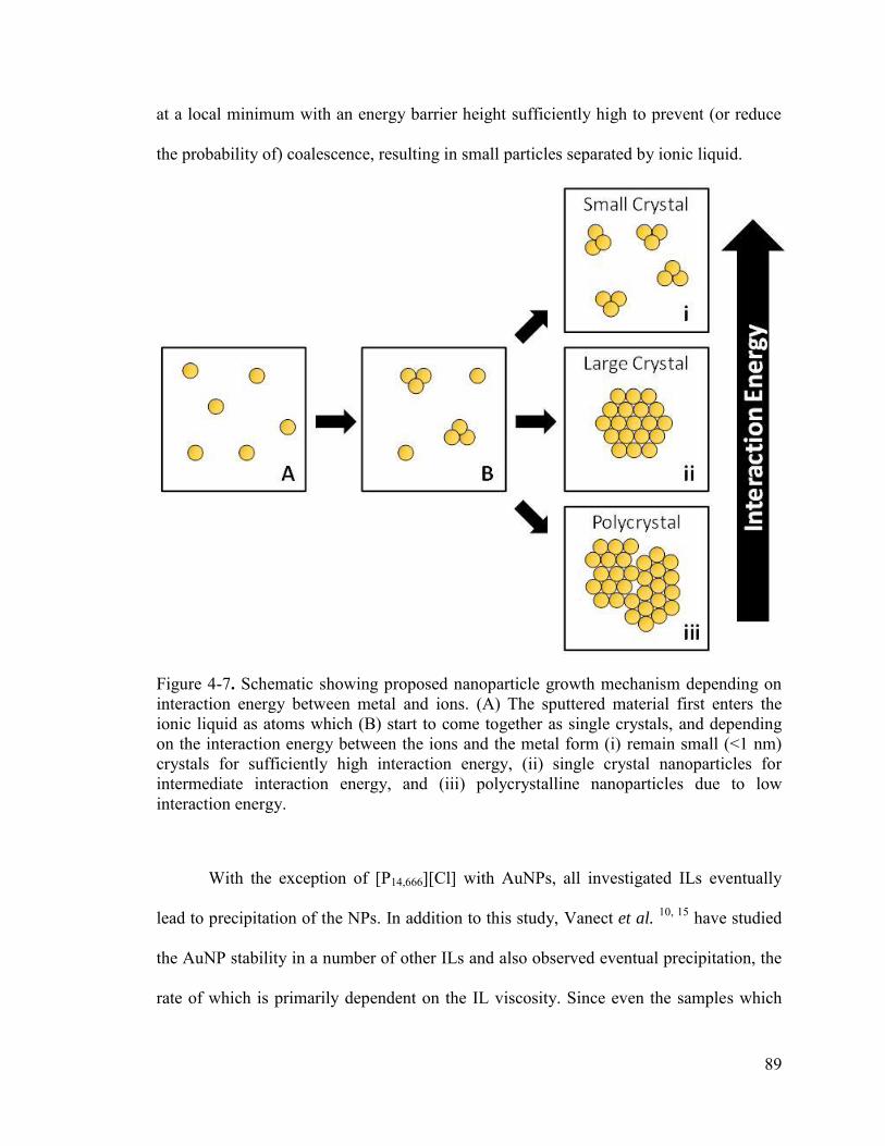
89
at a local minimum with an energy barrier height sufficiently high to prevent (or reduce
the probability of) coalescence, resulting in small particles separated by ionic liquid.
Figure 4-7. Schematic showing proposed nanoparticle growth mechanism depending on interaction energy between metal and ions. (A) The sputtered material first enters the ionic liquid as atoms which (B) start to come together as single crystals, and depending on the interaction energy between the ions and the metal form (i) remain small (<1 nm) crystals for sufficiently high interaction energy, (ii) single crystal nanoparticles for intermediate interaction energy, and (iii) polycrystalline nanoparticles due to low interaction energy.
With the exception of [P14,666][Cl] with AuNPs, all investigated ILs eventually
lead to precipitation of the NPs. In addition to this study, Vanect et al. 10, 15 have studied
the AuNP stability in a number of other ILs and also observed eventual precipitation, the
rate of which is primarily dependent on the IL viscosity. Since even the samples which
90
showed accumulations of small NPs showed precipitation, it is possible that the
accumulations of NPs eventually leads to coalescence and formation of larger particles
which are less likely to be captured when collecting near the top of the sample for TEM
imaging. Another explanation is that the accumulations are behaving as one large mass
similar to large particles, and the underlying IL does not provide adequate support to
prevent the accumulation from crashing out.
Demonstration of decreased particle growth rate
The growth rate of particles can be assumed to be dependent on and limited by the
collision rate (ν) between two particles based on the following equation:31
3bk T
a
(4-2)
where kb is Boltzmann’s constant, T is temperature, ϕ is the particle volumetric
concentration, η is viscosity, and a is the particle radius. The temperature plays a very
significant role in the particle diffusion and collision rate since the viscosity of ILs is
inversely proportional to temperature.32 As discussed previously, the metal atoms or
clusters must also overcome the attractive energy between the ions and the metal surface
in order to form larger particles. Decreasing the thermal energy of the solution would
therefore decrease the probability of overcoming this barrier. The combination of these
two factors suggests a significant increase in the stability of the solution.
Figure 4-8 shows the UV–Vis spectra of the [emim][EtSO4] with AuNPs using
the previously described procedures to compare the effect of decreased storage
temperature. The spectrum shows very little change from the measurement just after
deposition (Day 0) at a storage temperature of -5 °C indicating very little particle growth.
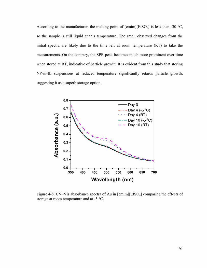
91
According to the manufacturer, the melting point of [emim][EtSO4] is less than -30 °C,
so the sample is still liquid at this temperature. The small observed changes from the
initial spectra are likely due to the time left at room temperature (RT) to take the
measurements. On the contrary, the SPR peak becomes much more prominent over time
when stored at RT, indicative of particle growth. It is evident from this study that storing
NP-in-IL suspensions at reduced temperature significantly retards particle growth,
suggesting it as a superb storage option.
Figure 4-8. UV–Vis absorbance spectra of Au in [emim][EtSO4] comparing the effects of storage at room temperature and at -5 °C.
92
In addition, [N10,111][Beti] (prepared in-house by Dr. Baker, University of
Missouri), which has a melting temperature of about 25 °C, was further investigated at
storage temperatures of +5 °C, i.e. the liquid was solidified with the deposited NPs during
storage. Figure 4-9(a) shows the SPR absorbance change from the first UV–Vis
measurement as a function of time for a sample left at room temperature just after Au
deposition and one stored at +5 °C for about 27 days before leaving at RT. Plotting the
change in absorbance over time after being left at room temperature in Figure 4-9(b), the
trends are very similar. The initially faster growth of the sample stored at +5 °C is due to
the growth which occurred when the sample was brought up to RT to perform the
previous measurements.
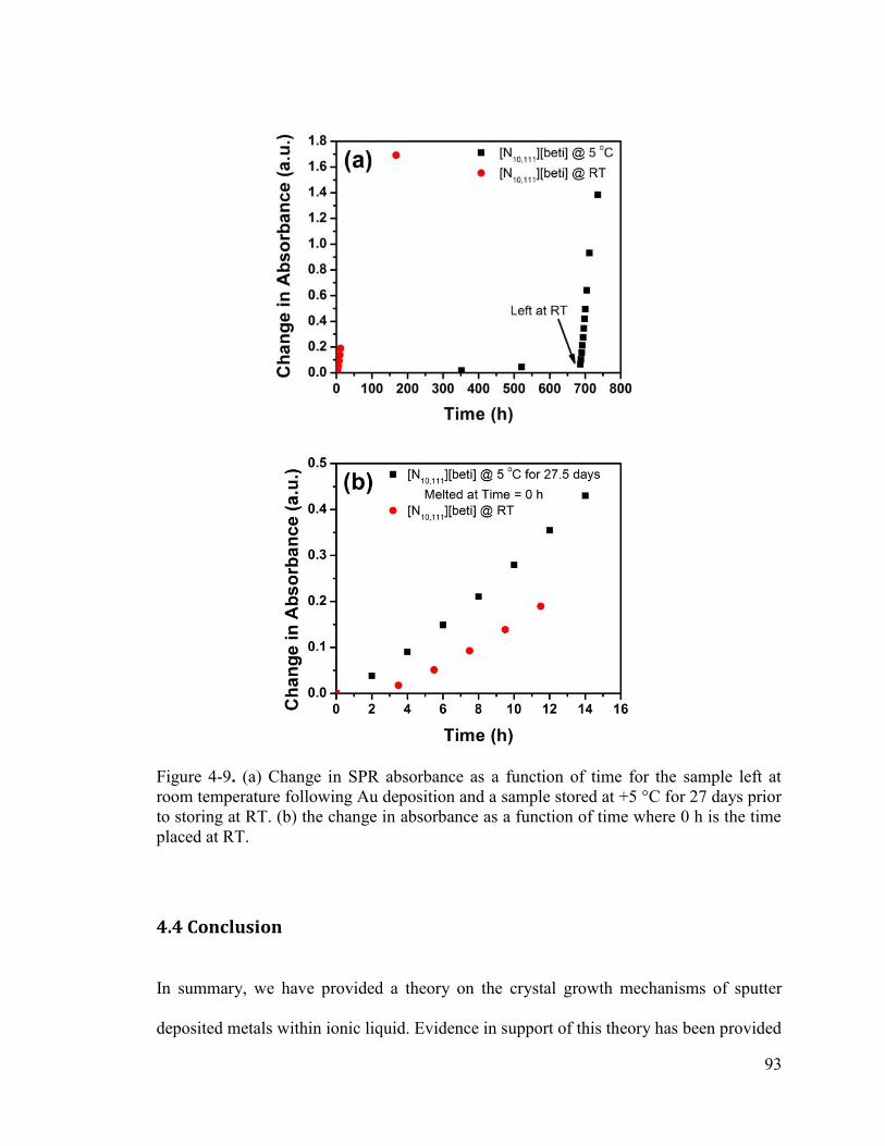
93
Figure 4-9. (a) Change in SPR absorbance as a function of time for the sample left at room temperature following Au deposition and a sample stored at +5 °C for 27 days prior to storing at RT. (b) the change in absorbance as a function of time where 0 h is the time placed at RT.
4.4 Conclusion
In summary, we have provided a theory on the crystal growth mechanisms of sputter
deposited metals within ionic liquid. Evidence in support of this theory has been provided
94
by investigating the particle structures developed in ionic liquids with different anions.
The developed theory presents a pathway towards potential long-term stability and
nanoparticle size control using ionic liquids with highly charge-localized anions. Such
ionic liquids will need to be investigated to take advantage of the electrochemical
enhancements brought on by the incorporation of these nanoparticles demonstrated in
Chapter 5.
95
4.5 References
Portions of this chapter consist of published information, which can be found within the following article: Hamm, S. C.; Basuray, S.; Mukherjee, S.; Sengupta, S.; Mathai, J. C.; Baker, G. A.; Gangopadhyay, S., Ionic conductivity enhancement of sputtered gold nanoparticle-in-ionic liquid electrolytes. Journal of Materials Chemistry A 2014, 2, 792-803. <http://pubs.rsc.org/en/content/articlehtml/2014/ta/c3ta13431h> - Reproduced by permission of The Royal Society of Chemistry
1. Galiński, M.; Lewandowski, A.; Stępniak, I., Ionic liquids as electrolytes. Electrochim. Acta 2006, 51, 5567-5580.
2. Lee, S.-g., Functionalized imidazolium salts for task-specific ionic liquids and their applications. Chem. Commun. 2006, 0, 1049-1063.
3. Giernoth, R., Task-Specific Ionic Liquids. Angew. Chem. Int. Ed. 2010, 49, 2834-2839.
4. Fredlake, C. P.; Crosthwaite, J. M.; Hert, D. G.; Aki, S. N. V. K.; Brennecke, J. F., Thermophysical Properties of Imidazolium-Based Ionic Liquids. J. Chem. Eng. Data
2004, 49, 954-964.
5. Burrell, A. K.; Sesto, R. E. D.; Baker, S. N.; McCleskey, T. M.; Baker, G. A., The large scale synthesis of pure imidazolium and pyrrolidinium ionic liquids. Green Chem.
2007, 9, 449-454.
6. Hapiot, P.; Lagrost, C., Electrochemical reactivity in room-temperature ionic liquids. Chem. Rev. 2008, 108, 2238-2264.
7. Torimoto, T.; Okazaki, K.-i.; Kiyama, T.; Hirahara, K.; Tanaka, N.; Kuwabata, S., Sputter deposition onto ionic liquids: Simple and clean synthesis of highly dispersed ultrafine metal nanoparticles. Appl. Phys. Lett. 2006, 89, 243117-243117-3.
96
8. Okazaki, K.-i.; Kiyama, T.; Hirahara, K.; Tanaka, N.; Kuwabata, S.; Torimoto, T., Single-step synthesis of gold–silver alloy nanoparticles in ionic liquids by a sputter deposition technique. Chem. Commun. 2008, 691-693.
9. Suzuki, T.; Suzuki, S.; Tomita, Y.; Okazaki, K.-i.; Shibayama, T.; Kuwabata, S.; Torimoto, T., Fabrication of Transition Metal Oxide Nanoparticles Highly Dispersed in Ionic Liquids by Sputter Deposition. Chem. Lett. 2010, 39, 1072-1074.
10. Vanecht, E.; Binnemans, K.; Seo, J. W.; Stappers, L.; Fransaer, J., Growth of sputter-deposited gold nanoparticles in ionic liquids. Phys. Chem. Chem. Phys. 2011, 13, 13565-13571.
11. Richter, K.; Birkner, A.; Mudring, A.-V., Stability and growth behavior of transition metal nanoparticles in ionic liquids prepared by thermal evaporation: how stable are they really? Phys. Chem. Chem. Phys. 2011, 13, 7136-7141.
12. Wender, H.; Andreazza, M. L.; Correia, R. R.; Teixeira, S. R.; Dupont, J., Synthesis of gold nanoparticles by laser ablation of an Au foil inside and outside ionic liquids. Nanoscale 2011, 3, 1240-1245.
13. Oda, Y.; Hirano, K.; Yoshii, K.; Kuwabata, S.; Torimoto, T.; Miura, M., Palladium Nanoparticles in Ionic Liquid by Sputter Deposition as Catalysts for Suzuki-Miyaura Coupling in Water. Chem. Lett. 2010, 39, 1069-1071.
14. Hamm, S. C.; Shankaran, R.; Korampally, V.; Bok, S.; Praharaj, S.; Baker, G. A.; Robertson, J. D.; Lee, B. D.; Sengupta, S.; Gangopadhyay, K.; Gangopadhyay, S., Sputter-Deposition of Silver Nanoparticles into Ionic Liquid as a Sacrificial Reservoir in Antimicrobial Organosilicate Nanocomposite Coatings. ACS Appl. Mater. Interfaces
2012, 4, 178-184.
15. Vanecht, E.; Binnemans, K.; Patskovsky, S.; Meunier, M.; Seo, J. W.; Stappers, L.; Fransaer, J., Stability of sputter-deposited gold nanoparticles in imidazolium ionic liquids. Phys. Chem. Chem. Phys. 2012, 14, 5662-5671.
16. Tokuda, H.; Hayamizu, K.; Ishii, K.; Susan, M. A. B. H.; Watanabe, M., Physicochemical properties and structures of room temperature ionic liquids. 1. Variation of anionic species. J. Phys. Chem. B 2004, 108, 16593-16600.
97
17. Tokuda, H.; Tsuzuki, S.; Susan, M. A. B. H.; Hayamizu, K.; Watanabe, M., How Ionic Are Room-Temperature Ionic Liquids? An Indicator of the Physicochemical Properties. J. Phys. Chem. B 2006, 110, 19593-19600.
18. Crosthwaite, J. M.; Muldoon, M. J.; Dixon, J. K.; Anderson, J. L.; Brennecke, J. F., Phase transition and decomposition temperatures, heat capacities and viscosities of pyridinium ionic liquids. J. Chem. Thermodyn. 2005, 37, 559-568.
19. Shields, S. P.; Richards, V. N.; Buhro, W. E., Nucleation Control of Size and Dispersity in Aggregative Nanoparticle Growth. A Study of the Coarsening Kinetics of Thiolate-Capped Gold Nanocrystals. Chem. Mater. 2010, 22, 3212-3225.
20. Balavinayagam, R.; Somik, M.; Cherian, J. M.; Keshab, G.; Shubhra, G., Sub-2 nm size and density tunable platinum nanoparticles using room temperature tilted-target sputtering. Nanotechnol. 2013, 24, 205602.
21. Dupont, J.; Scholten, J. D., On the structural and surface properties of transition-metal nanoparticles in ionic liquids. Chem. Soc. Rev. 2010, 39, 1780-1804.
22. Prasher, R.; Bhattacharya, P.; Phelan, P. E., Thermal Conductivity of Nanoscale Colloidal Solutions (Nanofluids). Phys Rev Lett 2005, 94, 025901.
23. Alvarez, M. M.; Khoury, J. T.; Schaaff, T. G.; Shafigullin, M. N.; Vezmar, I.; Whetten, R. L., Optical Absorption Spectra of Nanocrystal Gold Molecules. J. Phys.
Chem. B 1997, 101, 3706-3712.
24. Canongia Lopes, J. N.; Pádua, A. A.; Shimizu, K., Molecular force field for ionic liquids IV: Trialkylimidazolium and alkoxycarbonyl-imidazolium cations; alkylsulfonate and alkylsulfate anions. J. Phys. Chem. B 2008, 112, 5039-5046.
25. Tsuzuki, S.; Tokuda, H.; Hayamizu, K.; Watanabe, M., Magnitude and Directionality of Interaction in Ion Pairs of Ionic Liquids: Relationship with Ionic Conductivity. J. Phys. Chem. B 2005, 109, 16474-16481.
26. Vollmer, C.; Janiak, C., Naked metal nanoparticles from metal carbonyls in ionic liquids: Easy synthesis and stabilization. Coord. Chem. Rev. 2011, 255, 2039-2057.
27. Wender, H.; de Oliveira, L. F.; Migowski, P.; Feil, A. F.; Lissner, E.; Prechtl, M. H. G.; Teixeira, S. R.; Dupont, J., Ionic Liquid Surface Composition Controls the Size of
98
Gold Nanoparticles Prepared by Sputtering Deposition. J. Phys. Chem. C 2010, 114, 11764-11768.
28. Redel, E.; Walter, M.; Thomann, R.; Hussein, L.; Kruger, M.; Janiak, C., Stop-and-go, stepwise and "ligand-free" nucleation, nanocrystal growth and formation of Au-NPs in ionic liquids (ILs). Chem. Commun. 2010, 46, 1159-1161.
29. Campbell, C. T.; Parker, S. C.; Starr, D. E., The Effect of Size-Dependent Nanoparticle Energetics on Catalyst Sintering. Science 2002, 298, 811-814.
30. Ueno, K.; Inaba, A.; Kondoh, M.; Watanabe, M., Colloidal stability of bare and polymer-grafted silica nanoparticles in ionic liquids. Langmuir 2008, 24, 5253-5259.
31. Kraynov, A.; Müller, T. E.; Handy, S., Concepts for the Stabilization of Metal Nanoparticles in Ionic Liquids. Application of Ionic Liquids in Science and Technology
2011.
32. Hatakeyama, Y.; Takahashi, S.; Nishikawa, K., Can Temperature Control the Size of Au Nanoparticles Prepared in Ionic Liquids by the Sputter Deposition Technique? J.
Phys. Chem. C 2010, 114, 11098-11102.
99
Chapter 5 – Electrochemical Enhancement of Nanoparticle-in-ionic
liquid based electrolytes for Supercapacitor Applications
5.1 Introduction
As mentioned in Chapter 4, the highly desirable electrochemical properties have
warranted extensive investigation of ILs as electrolytes within electrochemical double-
layer capacitors. As a result, significant discussion of the interaction of the ions with
charged surfaces has occurred. For instance, the measured double-layer capacitance (Cdl)
is a function of the ion sizes,1, 2 as well as the specific and non-specific adsorption of
anions or cations on the electrode surface.3 Imidazolium-based cations adsorb to the
surface of metals (Au, Pt, etc.) due to π-bonding which results in adsorption-induced
pseudocapacitance.2 Sum frequency generation spectroscopy showed that imidazolium-
based cations at an electrified surface change orientation, from normal to parallel to the
surface at small and large anodic potential, respectively, with respect to the potential of
zero charge (the applied potential resulting in no inherent charge on the electrode).4-6
Such orientation of the ions affects Cdl by specifically altering the capacitive length-
scales at the ion-surface interface. Further, it has been observed that the different
diffusion coefficients of the ions leads to anomalous behavior, where the cation diffuses
faster despite it being larger than the anions in the investigated IL.7 High ion
concentrations in ILs have also shown anomalous increase in Cdl with increasing
temperature.1, 8 This behavior is attributed to the decrease in ion-pairing due to increased
thermal energy, which results in lower viscosity and increased conductivity, allowing
more ions to adsorb and interact near the surface.1, 9 Prediction of the behavior of ILs at
100
charged surfaces using different modeling techniques have been complicated by the
complexity of such systems and hence the best validation tools for the dependence of the
IL is still experimental observations.10, 11
As discussed in Chapter 1, the electrochemical measurements of some NP-in-ILs
have been investigated. However, to our knowledge no one has studied the
electrochemical properties of the nanocomposites by sputter deposition, which provides
the ability for a time-resolved investigation into how the size of the nanoparticles affects
the properties. In this work, we demonstrate enhanced double-layer capacitance and ionic
conductivity from the sputtered nanoparticle-in-IL electrolytes from Chapter 4 through
cyclic voltammetry (CV), ionic conductivity probe, and electrochemical impedance
spectroscopy (EIS) measurements. An explanation of the possible interactions of the NPs
with the IL is provided to illustrate the complex nature of the electrode-IL interface.
These results suggest these sputtered NP-in-IL electrolytes should be investigated further
for improved energy storage and quicker device response for applications ranging from
EDLCs to sensors.
5.2 Materials and Methods
Electrochemical cell preparation.
Cell 1: Au-coated stainless steel sheets were cut into 1 mm and 3 mm wide strips to a
length of about 1 cm, used as the working and counter electrodes, respectively. A 0.5 mm
diameter Pt wire was used as a pseudo-reference electrode (PSE). The sheets were
soldered to copper leads and the three electrodes were placed about 5 mm into the IL
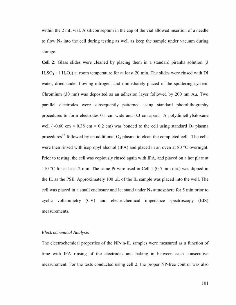
101
within the 2 mL vial. A silicon septum in the cap of the vial allowed insertion of a needle
to flow N2 into the cell during testing as well as keep the sample under vacuum during
storage.
Cell 2: Glass slides were cleaned by placing them in a standard piranha solution (3
H2SO4 : 1 H2O2) at room temperature for at least 20 min. The slides were rinsed with DI
water, dried under flowing nitrogen, and immediately placed in the sputtering system.
Chromium (30 nm) was deposited as an adhesion layer followed by 200 nm Au. Two
parallel electrodes were subsequently patterned using standard photolithography
procedures to form electrodes 0.1 cm wide and 0.3 cm apart. A polydimethylsiloxane
well (~0.60 cm × 0.38 cm × 0.2 cm) was bonded to the cell using standard O2 plasma
procedures12 followed by an additional O2 plasma to clean the completed cell. The cells
were then rinsed with isopropyl alcohol (IPA) and placed in an oven at 80 °C overnight.
Prior to testing, the cell was copiously rinsed again with IPA, and placed on a hot plate at
110 °C for at least 2 min. The same Pt wire used in Cell 1 (0.5 mm dia.) was dipped in
the IL as the PSE. Approximately 100 µL of the IL sample was placed into the well. The
cell was placed in a small enclosure and let stand under N2 atmosphere for 5 min prior to
cyclic voltammetry (CV) and electrochemical impedance spectroscopy (EIS)
measurements.
Electrochemical Analysis
The electrochemical properties of the NP-in-IL samples were measured as a function of
time with IPA rinsing of the electrodes and baking in between each consecutive
measurement. For the tests conducted using cell 2, the proper NP-free control was also
102
measured immediately following the NP sample in an attempt to remove error due to
atmospheric changes. For instance, we observed the electrochemical properties of
[emim][EtSO4] to be significantly affected by humidity due to the intrinsic hygroscopic
and hydrophilic nature of the IL.
Cyclic voltammetry was performed using a CH Instruments CHI800B
Electrochemical Analyzer. The cathodic and anodic breakdown limitations of the IL were
studied by gradually increasing the upper and lower voltage limits until a sharp increase
in current was observed using a rate of 100 mV s-1 and steps of 1 mV. Due to the
inconsistency of electrode area within Cell 1, the breakdown positions were taken at a
point just prior to the sharp increase in current. The breakdown positions of Cell 2 were
taken arbitrarily at 2 mA cm-2. A sweep from -1 to 1 V vs. PSE was also performed on
[emim][EtSO4] using Cell 2 to obtain a more accurate representation of the formed Cdl,
the range of which was chosen as it is well within the anodic and cathodic breakdown
limits of [emim][EtSO4] which was found to be approximately ±2.3 V at 2 mA cm-2. All
CV measurements were cycled ten times before collecting the data for evaluation.
Zheng et al. 13, 14 suggested that multiple CV scan rates should be performed to
construct a model of the system based on CV data, which can then be compared to EIS
data. However, the comparatively lengthy times required for multiple scans would result
in errors when evaluating the data since the particles are continuously growing. The
moderate scan rate of 100 mV s-1 was chosen so that the measurement could be taken in
a relatively quick manner (~7 min) while keeping the scan rate slow enough as to allow
adequate time for reactions to occur.
103
Ionic conductivities of the samples were measured using a Jenway 4520
conductivity probe. According to the manufacturer, the applied frequency is 800 Hz for
conductivities > 100 μS cm-1.
EIS was performed on the [emim][EtSO4] sample with 340 ppm Au using an
Agilent 4294A Impedance Analyzer with a 0.5 Vrms signal with frequencies between
40 Hz and 110 MHz. The model was fitted using Matlab via a code written by Jean-Luc
Dellis provided on the Mathworks website.
5.3 Results and Discussion
5.3.1 Potential Windows
The voltage windows of the ILs were studied as a function of time after deposition.
Figure 5-1 shows an example of [hmim][PF6] with 340 ppm v/v of Ag just after
deposition and 34 days after deposition. Immediately following deposition (Day 0, Figure
5-1(a)), the window decreased from about 3.8 V to 3.2 V, the cause of which will be
discussed further in the next section. After 34 days, the voltage window increased to
about 5.8 V, a 53 % increase in window with respect to the control as shown in Figure
5-1(b). The calculated window versus time after deposition is displayed in Figure 5-1(c).
As demonstrated in Table 5-1, some samples also showed increases in electrochemical
windows, while others had little or no change. Although the cause of this anomalous
increase is uncertain, it is plausible to assume that some of the increase in window may
be that the impurities (which causes decreased windows)15 adsorb to the nanoparticles.
As the nanoparticles precipitate, the impurities are removed, as well.
104
Figure 5-1. CV measurements taken (a) immediately following Ag deposition into [hmim][PF6], (b) after 34 days after deposition, and (c) calculated CV voltage windows over time after deposition. Dashed lines are provided to guide the eye only. The black line in (c) represents the control value.
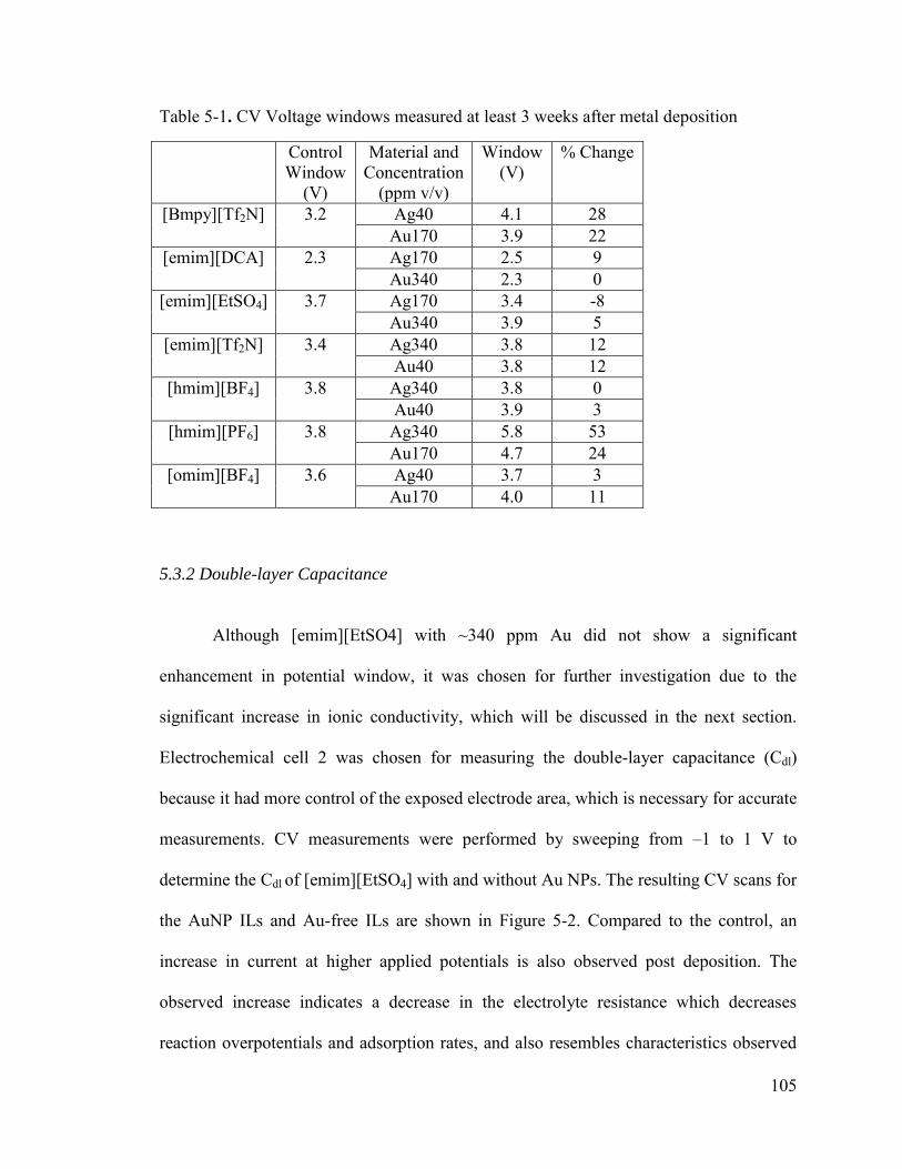
105
Table 5-1. CV Voltage windows measured at least 3 weeks after metal deposition
Control Window
(V)
Material and Concentration
(ppm v/v)
Window (V)
% Change
[Bmpy][Tf2N] 3.2 Ag40 4.1 28 Au170 3.9 22
[emim][DCA] 2.3 Ag170 2.5 9 Au340 2.3 0
[emim][EtSO4] 3.7 Ag170 3.4 -8 Au340 3.9 5
[emim][Tf2N] 3.4 Ag340 3.8 12 Au40 3.8 12
[hmim][BF4] 3.8 Ag340 3.8 0 Au40 3.9 3
[hmim][PF6] 3.8 Ag340 5.8 53 Au170 4.7 24
[omim][BF4] 3.6 Ag40 3.7 3 Au170 4.0 11
5.3.2 Double-layer Capacitance
Although [emim][EtSO4] with ~340 ppm Au did not show a significant
enhancement in potential window, it was chosen for further investigation due to the
significant increase in ionic conductivity, which will be discussed in the next section.
Electrochemical cell 2 was chosen for measuring the double-layer capacitance (Cdl)
because it had more control of the exposed electrode area, which is necessary for accurate
measurements. CV measurements were performed by sweeping from –1 to 1 V to
determine the Cdl of [emim][EtSO4] with and without Au NPs. The resulting CV scans for
the AuNP ILs and Au-free ILs are shown in Figure 5-2. Compared to the control, an
increase in current at higher applied potentials is also observed post deposition. The
observed increase indicates a decrease in the electrolyte resistance which decreases
reaction overpotentials and adsorption rates, and also resembles characteristics observed
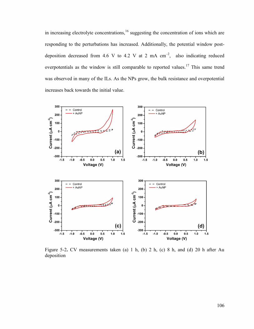
106
in increasing electrolyte concentrations,16 suggesting the concentration of ions which are
responding to the perturbations has increased. Additionally, the potential window post-
deposition decreased from 4.6 V to 4.2 V at 2 mA cm–2, also indicating reduced
overpotentials as the window is still comparable to reported values.17 This same trend
was observed in many of the ILs. As the NPs grow, the bulk resistance and overpotential
increases back towards the initial value.
Figure 5-2. CV measurements taken (a) 1 h, (b) 2 h, (c) 8 h, and (d) 20 h after Au deposition
107
The effective Cdl was taken from the CV curves at the minimum point of Eq. (5.1)
( )2
f rdl
I I dEC
dt
(5-1)
where If and Ir are the forward and reverse sweep currents, respectively, and dE/dt is the
voltage sweep rate. It has been suggested, although debated, that the minimum value
corresponds to the potential of zero charge and is representative of the Cdl of the IL.3, 10
The calculated capacitance values are plotted versus time after deposition in Figure
5-3(a). Immediately following deposition, the measured capacitance is at the highest
measured value, up to 2.9x that of the control, subsequently decreasing exponentially
with increasing time (particle size). Figure 5-3(b) individually plots the forward and
reverse sweeping currents used in calculating Cdl versus time. It can be observed that
while the forward sweeping current remains comparable to the control, the reverse
sweeping current is the primary cause of the experimental increase in calculated
capacitance. The observed asymmetrical increase in current post deposition verifies that
the AuNPs are not promoting significant electrical conduction, as would be expected
since the Au concentration is orders lower than percolation limits.18 Rather, the results
suggest increased interaction between the cations and the Au electrode. It should be
mentioned that freely suspended AuNPs in IL can show quantized charging behavior.19
However, the derivatives of our CV curves did not result in any discernible charging
peaks, so we cannot conclude that it is a contributing mechanism for the observed
capacitance increase.
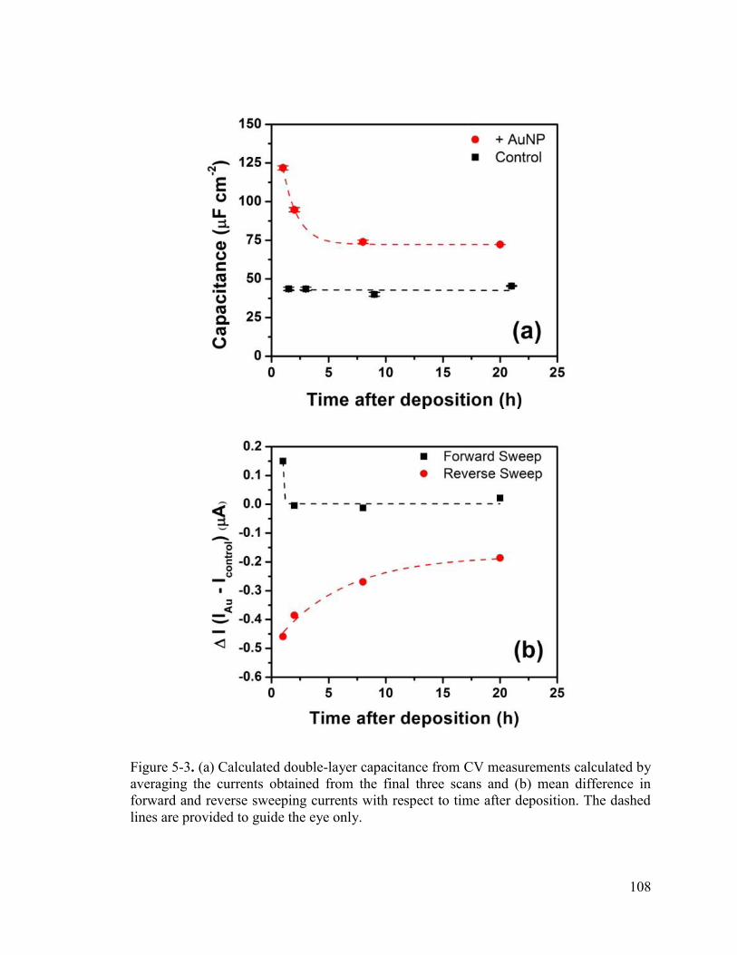
108
Figure 5-3. (a) Calculated double-layer capacitance from CV measurements calculated by averaging the currents obtained from the final three scans and (b) mean difference in forward and reverse sweeping currents with respect to time after deposition. The dashed lines are provided to guide the eye only.
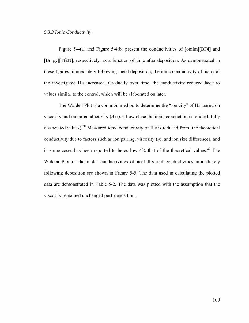
109
5.3.3 Ionic Conductivity
Figure 5-4(a) and Figure 5-4(b) present the conductivities of [omim][BF4] and
[Bmpy][Tf2N], respectively, as a function of time after deposition. As demonstrated in
these figures, immediately following metal deposition, the ionic conductivity of many of
the investigated ILs increased. Gradually over time, the conductivity reduced back to
values similar to the control, which will be elaborated on later.
The Walden Plot is a common method to determine the “ionicity” of ILs based on
viscosity and molar conductivity (Λ) (i.e. how close the ionic conduction is to ideal, fully
dissociated values).20 Measured ionic conductivity of ILs is reduced from the theoretical
conductivity due to factors such as ion pairing, viscosity (η), and ion size differences, and
in some cases has been reported to be as low 4% that of the theoretical values.20 The
Walden Plot of the molar conductivities of neat ILs and conductivities immediately
following deposition are shown in Figure 5-5. The data used in calculating the plotted
data are demonstrated in Table 5-2. The data was plotted with the assumption that the
viscosity remained unchanged post-deposition.
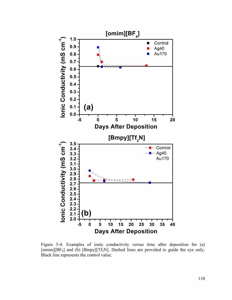
110
Figure 5-4. Examples of ionic conductivity versus time after deposition for (a) [omim][BF4] and (b) [Bmpy][Tf2N]. Dashed lines are provided to guide the eye only. Black line represents the control value.
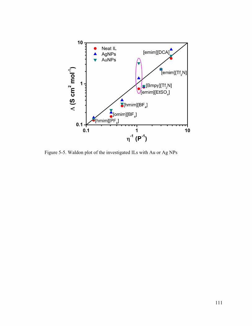
111
Figure 5-5. Waldon plot of the investigated ILs with Au or Ag NPs
112
Table 5-2. Parameters used to plot within the Waldon plot. Values were taken from the manufacturer unless specified otherwise.
ρ (g cm-3)
η (cP)
σcontrol (mS cm-1)
Material & Concentration
(ppm v/v)
σmetal (mS cm-1)
[emim][DCA] 1.0621 2121 25.0 Ag170 40.6 Au340 28.6
[emim][Tf2N] 1.524 3322 8.8 Ag340 8.7 Au40 8.9
[Bmpy][Tf2N] 1.39823 7323 2.8 Ag40 2.9 Au170 3.0
[emim][EtSO4] 1.239 92 24 4.0 Ag170 7.2 Au340 16.6*
[hmim][BF4] 1.149 19525 1.3 Ag170 1.8 Au40 1.5
[omim][BF4] 1.12 32525 0.6 Ag40 0.8 Au170 0.9
[hmim][PF6] 1.419 71126 0.6 Ag340 0.7 Au170 0.6
*taken from the ratio of σmetal/ σcontrol from EIS measurements and multiplied by the σcontrol measured from the probe.
From Figure 5-5, we can see that [emim][EtSO4] is the most affected by the
incorporation of metal NPs. Additionally, the general trend from these results indicate
that the anion plays an important role in the change in conductivity. The increase in
conductivity is greatest for the [EtSO4]– anion, followed by [DCA] –, [BF4] –, [PF6] –, and
finally [Tf2N]– which showed very little enhancement with NP incorporation. We can
eliminate enhanced electronic conduction as a possible explanation as mentioned
previously, which is also verified by the similar metal concentrations not showing
comparable enhancement. Additionally, enhanced conduction due to quantum charging
(if it were present) can be ruled out since the electron transfer rate is known to be slow,27
so electrons are incapable of responding to such high frequencies such as those described
113
in the next section. Therefore, if we assume the enhanced conduction is due to a change
in viscosity, using [emim][EtSO4] as an example, the AuNPs would have to decrease the
viscosity approximately 3x based on the Walden Plot to achieve the same conductivity
enhancement. A decrease in viscosity by the incorporation of NPs goes against Einstein’s
equations,28 but the incorporation of NPs into fluids has previously been observed to
provide anomalous decreased viscosity with reported values less than 50% those of the
controls.29-32 Regrettably, viscosity measurements could not be performed due to the
small quantity used in the study.
The incorporation of small NPs, with highest surface area and strongest anion
interaction energy, likely disrupts the well-ordered structure and separates ion
agglomerates within the IL. The disruption results in nanodomains consisting of free
cations with high self-diffusion coefficients resulting in an apparent decrease in viscosity.
Another plausible explanation is that the aforementioned structure disruption results in an
increase in free volume, which has been shown to be the limiting factor for viscosity and
ionic conductivity in ILs.33-35 The enhancement due to the disruption in the structure is
surely a factor controlled by the ion shape and location of charge, which will affect its
ability to structure around the NPs. As the NPs grow, the concentration of the disrupted
nanoscale domains decreases, resulting in a decrease in the enhanced electrochemical
properties.
114
5.3.4 Electrochemical Impedance Spectroscopy
EIS was used to analyze the frequency – dependent electrochemical interactions
between the IL [emim][EtSO4] and the electrodes. A Randles circuit, as shown in Figure
5-6(a), is typically used to describe electrolyte-electrode interactions obtained by EIS,36
and is represented by a capacitor in parallel with a resistor and Warburg element
connected in series. These elements represent Cdl, charge transfer resistance (Rct), and
diffusion, respectively. Additionally, a resistor is connected in series to represent the
electrolyte resistance (RE), and the capacitance of the cell is neglected. The Randles
circuit, however, assumes similar diffusion properties and interactions with the electrode
for both ions, which is not typically the case for ILs, as discussed previously. Therefore,
EIS was evaluated using the equivalent circuit model presented in Figure 5-6(b). The
model consists of three circuits, representative of the cation, anion, and the bulk
properties. The cation– and anion–electrode interactions can be represented individually
because the ions exhibit different diffusion properties.7, 37, 38 These ion – electrode
interfaces are represented by a modified Randles circuit in which Cdl and the Warburg
elements are replaced by constant phase elements (CPE) with an equivalent impedance of
σ(jω)-n, where σ is the constant, ω is the angular frequency, and n is an exponent
(0 ≤ n ≤ 1). A CPE element is typically used to replace Cdl due to inhomogeneity of the
ion–electrode interface.39, 40 We also chose to represent the Warburg element with a CPE
to account for non-ideal diffusive behavior, ion orientation changes under the applied AC
signal, as well as pseudocapacitive adsorption of ions.4, 41 Finally, the bulk resistance
(RHF) and capacitance (CHF) are represented by a parallel R-C circuit.42 It should be noted
that we deduced the high frequency (HF) results to be indicative of the bulk properties as
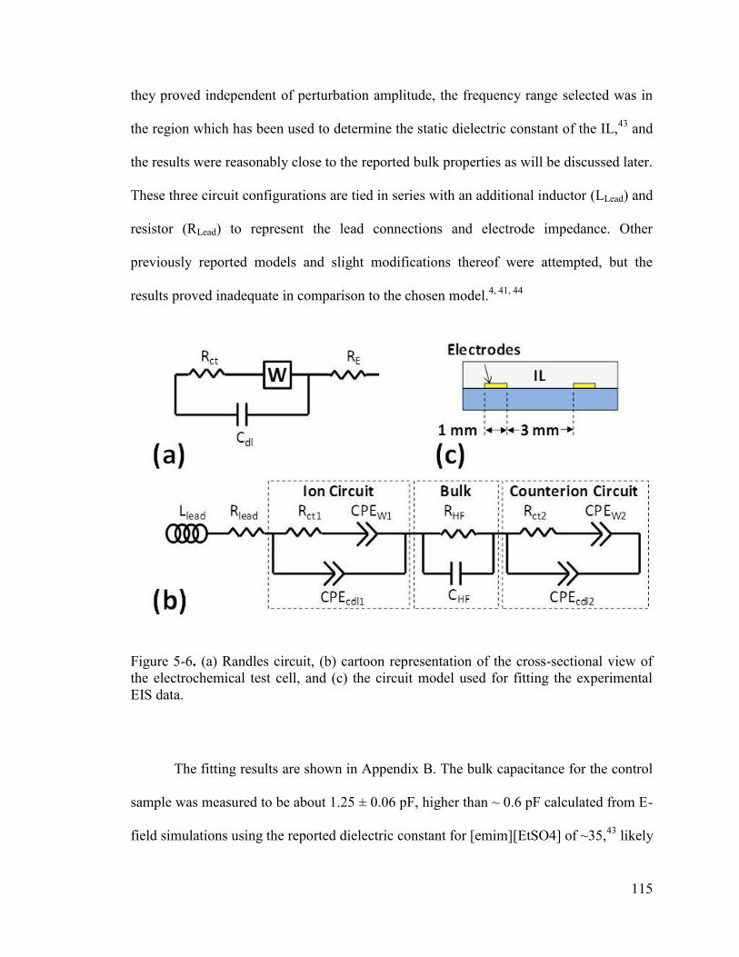
115
they proved independent of perturbation amplitude, the frequency range selected was in
the region which has been used to determine the static dielectric constant of the IL,43 and
the results were reasonably close to the reported bulk properties as will be discussed later.
These three circuit configurations are tied in series with an additional inductor (LLead) and
resistor (RLead) to represent the lead connections and electrode impedance. Other
previously reported models and slight modifications thereof were attempted, but the
results proved inadequate in comparison to the chosen model.4, 41, 44
Figure 5-6. (a) Randles circuit, (b) cartoon representation of the cross-sectional view of the electrochemical test cell, and (c) the circuit model used for fitting the experimental EIS data.
The fitting results are shown in Appendix B. The bulk capacitance for the control
sample was measured to be about 1.25 ± 0.06 pF, higher than ~ 0.6 pF calculated from E-
field simulations using the reported dielectric constant for [emim][EtSO4] of ~35,43 likely
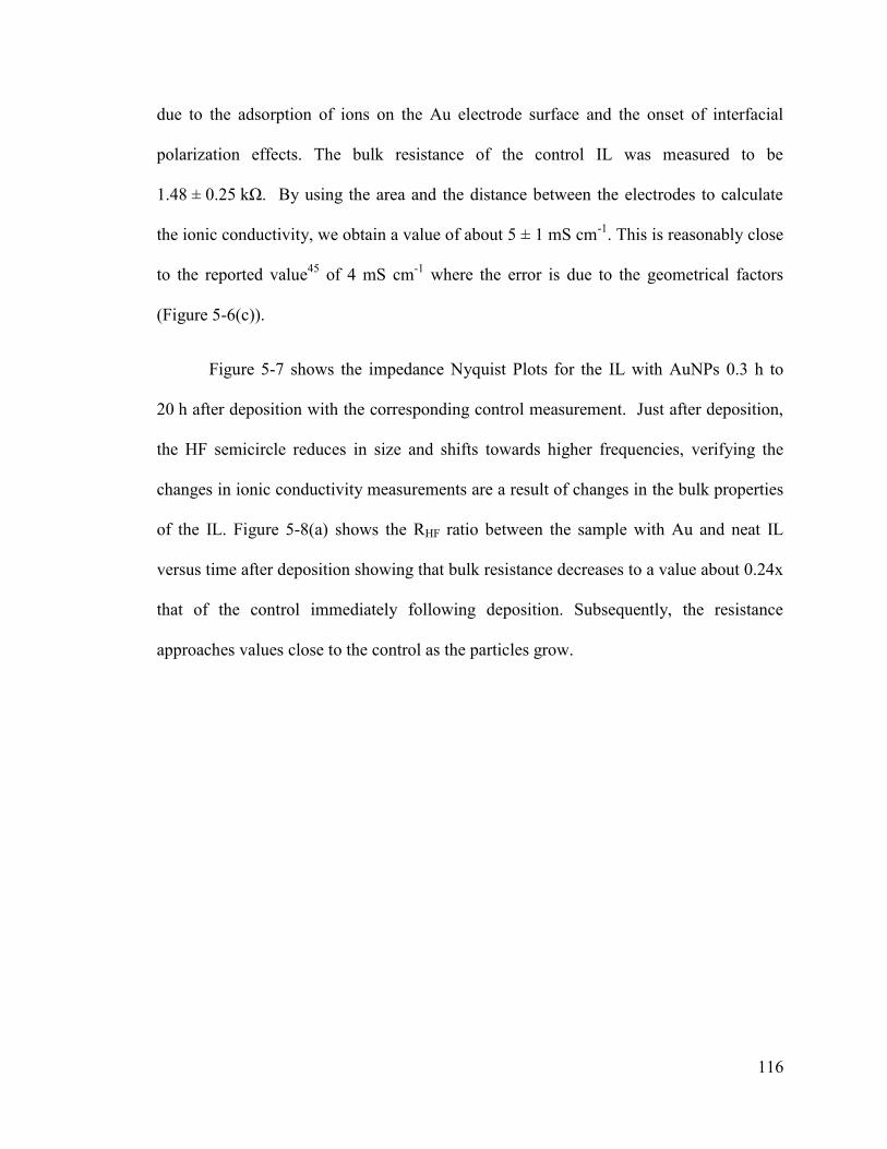
116
due to the adsorption of ions on the Au electrode surface and the onset of interfacial
polarization effects. The bulk resistance of the control IL was measured to be
1.48 ± 0.25 kΩ. By using the area and the distance between the electrodes to calculate
the ionic conductivity, we obtain a value of about 5 ± 1 mS cm-1. This is reasonably close
to the reported value45 of 4 mS cm-1 where the error is due to the geometrical factors
(Figure 5-6(c)).
Figure 5-7 shows the impedance Nyquist Plots for the IL with AuNPs 0.3 h to
20 h after deposition with the corresponding control measurement. Just after deposition,
the HF semicircle reduces in size and shifts towards higher frequencies, verifying the
changes in ionic conductivity measurements are a result of changes in the bulk properties
of the IL. Figure 5-8(a) shows the RHF ratio between the sample with Au and neat IL
versus time after deposition showing that bulk resistance decreases to a value about 0.24x
that of the control immediately following deposition. Subsequently, the resistance
approaches values close to the control as the particles grow.
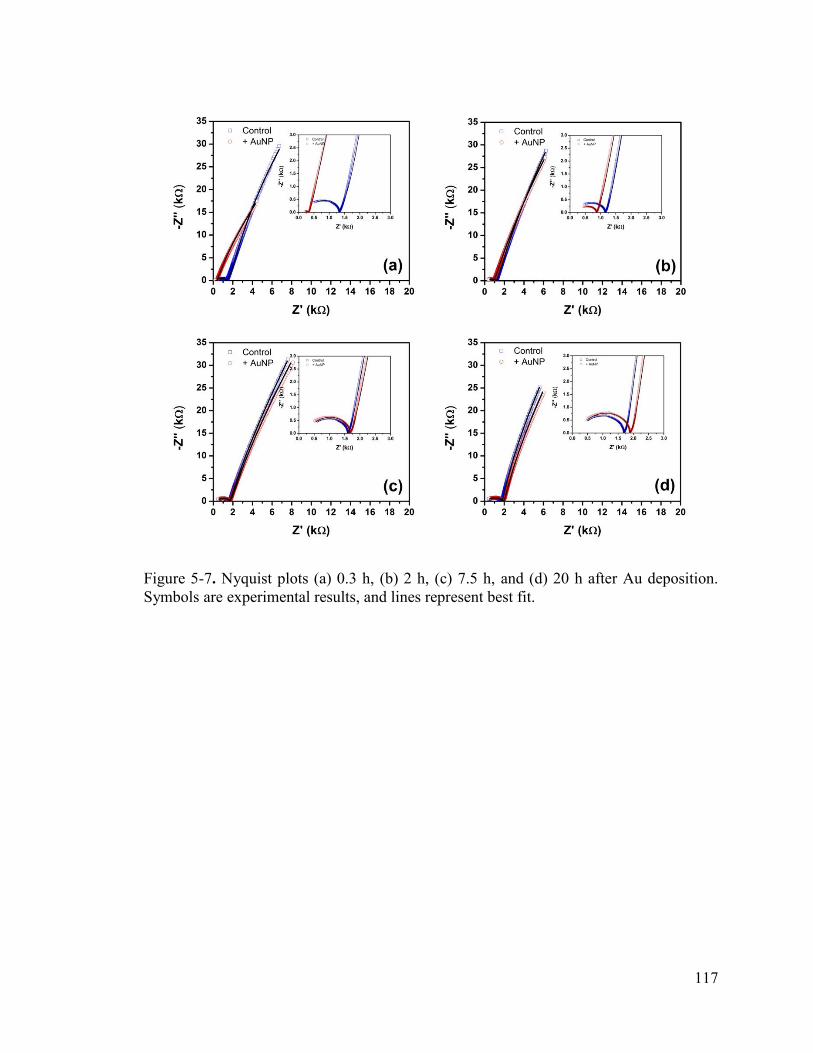
117
Figure 5-7. Nyquist plots (a) 0.3 h, (b) 2 h, (c) 7.5 h, and (d) 20 h after Au deposition. Symbols are experimental results, and lines represent best fit.
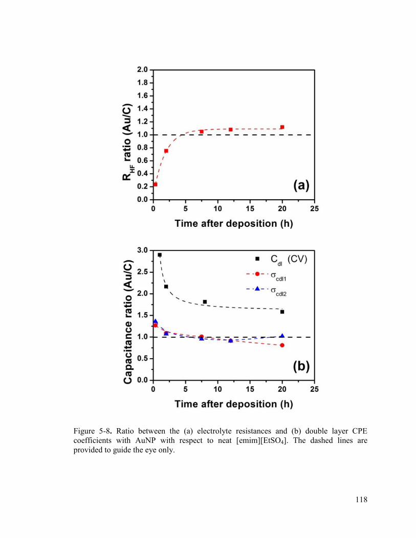
118
Figure 5-8. Ratio between the (a) electrolyte resistances and (b) double layer CPE coefficients with AuNP with respect to neat [emim][EtSO4]. The dashed lines are provided to guide the eye only.
119
The fitted results also indicate the bulk capacitance increases just after deposition.
The cause of which may be due to the decrease in electrolyte resistance. Decreased
resistance suggests increased mobility of the ions, requiring higher frequencies to achieve
a closer representation of bulk capacitance because of increased interfacial polarization
effects at lower frequencies, resulting in a higher measured capacitance as well as
increased fitting error.43 Additionally, the incorporation of conducting materials, such as
carbon nanotubes, into an electrolyte has also shown to increase bulk capacitance
measured in the HF regime.46
The impedance curves at lower frequencies result in a steep line, indicative of the
capacitive nature of the IL at the electrode surface. The fitting results show the ion double
layer CPEcdl1 exponent (n) is approximately 0.80 ± 0.02, whereas the counterion circuit
CPEcdl2 represents almost ideal capacitive behavior with an exponent of approximately 1.
The low exponent for the ion circuit is likely caused from the geometry of the cell
resulting in varying electric field and current densities across the surface. The Warburg
CPE exponents for the ion and counterion circuits are 0.34 ± 0.05 and 0.60 ± 0.03,
respectively. These results indicate a more capacitive behavior for the counterion circuit
and more resistive behavior for the ion circuit, the cause of which warrants further
investigation, but may be due to the specific adsorption of one of the ions on the Au
electrode surface.
The EIS results for the samples after Au incorporation show very similar behavior
to the control in the two low frequency circuits. One noticeable difference between them
is the value of the double layer CPE constants (σ), which increases up to 27% and 36%
just after deposition for the ion and counterion circuits, respectively, followed by an
120
approach to the control values over time (Figure 5-8(b)). This behavior resembles that
seen from the CV scans, although on a different scale, an issue which has been reported
when comparing the two measurement techniques.13
To reiterate, the observed electrochemical enhancements can be explained as an
effect of the adsorption of ions onto the NP surface. Sufficiently small, neutral Ag and
AuNPs resulting from sputter deposition are expected to attract anion adsorption due to
the electron deficient metal surface.47 The interaction energy between molecules and NPs
is also known to increase with decreasing NP size, owing to the low coordination
numbers of the atoms on the NP surface.48, 49 Higher interaction energies with the NP
surface is also expected of anions with more localized charges,50 such as that expected in
[EtSO4]. As mentioned previously, the attraction of anions to the NPs results in a change
in charge distribution and ionic liquid structure, seemingly dependent on the ionic
composition and anion charge distribution, consequently “freeing” additional cations to
respond and interact with the electrode surface, as well as decreasing the electrolyte
resistance (Figure 5-9). Indeed, the increase in currents at anodic potentials of the CV
scan indicates an increase in cation interaction with the electrode, suggesting the NPs are
attracting anions. Similarly, the decrease in electrolyte resistance observed indicates
increased self-diffusion coefficients of the ions caused by the aforementioned changes.
The total surface area and attractive energy of the NPs decreases as the NPs grow
resulting in a decrease in adsorbed anion strength and free cation concentrations with
time.
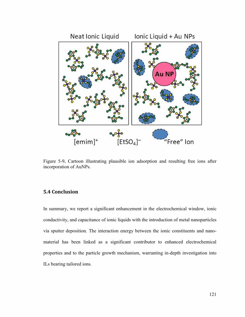
121
Figure 5-9. Cartoon illustrating plausible ion adsorption and resulting free ions after incorporation of AuNPs.
5.4 Conclusion
In summary, we report a significant enhancement in the electrochemical window, ionic
conductivity, and capacitance of ionic liquids with the introduction of metal nanoparticles
via sputter deposition. The interaction energy between the ionic constituents and nano-
material has been linked as a significant contributor to enhanced electrochemical
properties and to the particle growth mechanism, warranting in-depth investigation into
ILs bearing tailored ions.
122
5.5 References
Portions of this chapter consist of published information, which can be found within the following article: Hamm, S. C.; Basuray, S.; Mukherjee, S.; Sengupta, S.; Mathai, J. C.; Baker, G. A.; Gangopadhyay, S., Ionic conductivity enhancement of sputtered gold nanoparticle-in-ionic liquid electrolytes. Journal of Materials Chemistry A 2014, 2, 792-803. <http://pubs.rsc.org/en/content/articlehtml/2014/ta/c3ta13431h> - Reproduced by permission of The Royal Society of Chemistry
1. Lockett, V.; Sedev, R.; Ralston, J.; Horne, M.; Rodopoulos, T., Differential Capacitance of the Electrical Double Layer in Imidazolium-Based Ionic Liquids: Influence of Potential, Cation Size, and Temperature. J. Phys. Chem. C 2008, 112, 7486-7495.
2. Alam, M. T.; Islam, M. M.; Okajima, T.; Ohsaka, T., Capacitance Measurements in a Series of Room-Temperature Ionic Liquids at Glassy Carbon and Gold Electrode Interfaces. J. Phys. Chem. C 2008, 112, 16600-16608.
3. Lockett, V.; Horne, M.; Sedev, R.; Rodopoulos, T.; Ralston, J., Differential capacitance of the double layer at the electrode/ionic liquids interface. Phys. Chem.
Chem. Phys. 2010, 12, 12499-12512.
4. Baldelli, S., Surface Structure at the Ionic Liquid−Electrified Metal Interface. Acc. Chem. Res. 2008, 41, 421-431.
5. Rivera-Rubero, S.; Baldelli, S., Surface Spectroscopy of Room-temperature Ionic Liquids on a Platinum Electrode: A Sum Frequency Generation Study. J. Phys. Chem. B
2004, 108, 15133-15140.
6. Aliaga, C.; Santos, C. S.; Baldelli, S., Surface chemistry of room-temperature ionic liquids. Phys. Chem. Chem. Phys. 2007, 9, 3683-3700.
7. Tokuda, H.; Hayamizu, K.; Ishii, K.; Susan, M. A. B. H.; Watanabe, M., Physicochemical properties and structures of room temperature ionic liquids. 1. Variation of anionic species. J. Phys. Chem. B 2004, 108, 16593-16600.
123
8. Silva, F.; Gomes, C.; Figueiredo, M.; Costa, R.; Martins, A.; Pereira, C. M., The electrical double layer at the [BMIM][PF6] ionic liquid/electrode interface – Effect of temperature on the differential capacitance. J. Electroanal. Chem. 2008, 622, 153-160.
9. Holovko, M.; Kapko, V.; Henderson, D.; Boda, D., On the influence of ionic association on the capacitance of an electrical double layer. Chem. Phys. Lett. 2001, 341, 363-368.
10. Kornyshev, A. A., Double-Layer in Ionic Liquids: Paradigm Change? J. Phys.
Chem. B 2007, 111, 5545-5557.
11. Lauw, Y.; Horne, M. D.; Rodopoulos, T.; Nelson, A.; Leermakers, F. A. M., Electrical Double-Layer Capacitance in Room Temperature Ionic Liquids: Ion-Size and Specific Adsorption Effects. J. Phys. Chem. B 2010, 114, 11149-11154.
12. Bhattacharya, S.; Datta, A.; Berg, J. M.; Gangopadhyay, S., Studies on surface wettability of poly(dimethyl) siloxane (PDMS) and glass under oxygen-plasma treatment and correlation with bond strength. J. Microelectromech. Syst. 2005, 14, 590-597.
13. Zheng, J. P.; Goonetilleke, P. C.; Pettit, C. M.; Roy, D., Probing the electrochemical double layer of an ionic liquid using voltammetry and impedance spectroscopy: A comparative study of carbon nanotube and glassy carbon electrodes in [EMIM]+[EtSO4]−. Talanta 2010, 81, 1045-1055.
14. Zheng, J. P.; Pettit, C. M.; Goonetilleke, P. C.; Zenger, G. M.; Roy, D., D.C. voltammetry of ionic liquid-based capacitors: Effects of Faradaic reactions, electrolyte resistance and voltage scan speed investigated using an electrode of carbon nanotubes in EMIM-EtSO4. Talanta 2009, 78, 1056-1062.
15. Burrell, A. K.; Sesto, R. E. D.; Baker, S. N.; McCleskey, T. M.; Baker, G. A., The large scale synthesis of pure imidazolium and pyrrolidinium ionic liquids. Green Chem.
2007, 9, 449-454.
16. Yufei, C.; Cunnane, V. J.; Schiffrin, D. J.; Mutomaki, L.; Kontturi, K., Interfacial capacitance and ionic association at electrified liquid/liquid interfaces. J. Chem. Soc.,
Faraday Trans. 1991, 87, 107-114.
17. Holbrey, J. D.; Reichert, W. M.; Swatloski, R. P.; Broker, G. A.; Pitner, W. R.; Seddon, K. R.; Rogers, R. D., Efficient, halide free synthesis of new, low cost ionic
124
liquids: 1,3-dialkylimidazolium salts containing methyl- and ethyl-sulfate anions. Green
Chem. 2002, 4, 407-413.
18. Nan, C.-W.; Shen, Y.; Ma, J., Physical properties of composites near percolation. Annu. Rev. Mater. Res. 2010, 40, 131-151.
19. Mertens, S. F.; Vollmer, C.; Held, A.; Aguirre, M. H.; Walter, M.; Janiak, C.; Wandlowski, T., “Ligand‐Free” Cluster Quantized Charging in an Ionic Liquid. Angew.
Chem. Int. Ed. 2011, 50, 9735-9738.
20. MacFarlane, D. R.; Forsyth, M.; Izgorodina, E. I.; Abbott, A. P.; Annat, G.; Fraser, K., On the concept of ionicity in ionic liquids. Phys. Chem. Chem. Phys. 2009, 11, 4962-4967.
21. MacFarlane, D. R.; Golding, J.; Forsyth, S.; Forsyth, M.; Deacon, G. B., Low viscosity ionic liquids based on organic salts of the dicyanamide anion. Chem. Commun.
2001, 1430-1431.
22. Yao, H.; Zhang, S.; Wang, J.; Zhou, Q.; Dong, H.; Zhang, X., Densities and Viscosities of the Binary Mixtures of 1-Ethyl-3-methylimidazolium Bis (trifluoromethylsulfonyl) imide with N-Methyl-2-pyrrolidone or Ethanol at T=(293.15 to 323.15) K. J. Chem. Eng. Data 2012, 57, 875-881.
23. Shamsipur, M.; Beigi, A. A. M.; Teymouri, M.; Pourmortazavi, S. M.; Irandoust, M., Physical and electrochemical properties of ionic liquids 1-ethyl-3-methylimidazolium tetrafluoroborate, 1-butyl-3-methylimidazolium trifluoromethanesulfonate and 1-butyl-1-methylpyrrolidinium bis (trifluoromethylsulfonyl) imide. J. Mol. Liq. 2010, 157, 43-50.
24. Torrecilla, J. S.; Rafione, T.; García, J.; Rodríguez, F., Effect of Relative Humidity of Air on Density, Apparent Molar Volume, Viscosity, Surface Tension, and Water Content of 1-Ethyl-3-methylimidazolium Ethylsulfate Ionic Liquid. J. Chem. Eng.
Data 2008, 53, 923-928.
25. Zhu, A.; Wang, J.; Liu, R., A volumetric and viscosity study for the binary mixtures of 1-hexyl-3-methylimidazolium tetrafluoroborate with some molecular solvents. J. Chem. Thermodyn. 2011, 43, 796-799.
26. Tomida, D.; Kumagai, A.; Kenmochi, S.; Qiao, K.; Yokoyama, C., Viscosity of 1-hexyl-3-methylimidazolium hexafluorophosphate and 1-octyl-3-methylimidazolium hexafluorophosphate at high pressure. J. Chem. Eng. Data 2007, 52, 577-579.
125
27. Chen, S.; Pei, R., Ion-induced rectification of nanoparticle quantized capacitance charging in aqueous solutions. J. Am. Chem. Soc. 2001, 123, 10607-10615.
28. Einstein, A.; Fürth, R., Investigations on the Theory of the Brownian Movement. DOVER PUBN Incorporated: 1956.
29. Tuteja, A.; Duxbury, P. M.; Mackay, M. E., Multifunctional Nanocomposites with Reduced Viscosity. Macromolecules 2007, 40, 9427-9434.
30. Grabowski, C. A.; Adhikary, B.; Mukhopadhyay, A., Dynamics of gold nanoparticles in a polymer melt. Appl. Phys. Lett. 2009, 94, 021903.
31. Roberts, C.; Cosgrove, T.; Schmidt, R. G.; Gordon, G. V., Diffusion of Poly(dimethylsiloxane) Mixtures with Silicate Nanoparticles. Macromolecules 2000, 34, 538-543.
32. Mackay, M. E.; Dao, T. T.; Tuteja, A.; Ho, D. L.; Van Horn, B.; Kim, H.-C.; Hawker, C. J., Nanoscale effects leading to non-Einstein-like decrease in viscosity. Nat.
Mater. 2003, 2, 762-766.
33. Abbott, A. P., Application of Hole Theory to the Viscosity of Ionic and Molecular Liquids. ChemPhysChem 2004, 5, 1242-1246.
34. Abbott, A. P., Model for the Conductivity of Ionic Liquids Based on an Infinite Dilution of Holes. ChemPhysChem 2005, 6, 2502-2505.
35. Abbott, A. P.; Harris, R. C.; Ryder, K. S., Application of Hole Theory to Define Ionic Liquids by their Transport Properties†. J. Phys. Chem. B 2007, 111, 4910-4913.
36. Basuray, S.; Senapati, S.; Aijian, A.; Mahon, A. R.; Chang, H.-C., Shear and AC Field Enhanced Carbon Nanotube Impedance Assay for Rapid, Sensitive, and Mismatch-Discriminating DNA Hybridization. ACS Nano 2009, 3, 1823-1830.
37. Tokuda, H.; Tsuzuki, S.; Susan, M. A. B. H.; Hayamizu, K.; Watanabe, M., How Ionic Are Room-Temperature Ionic Liquids? An Indicator of the Physicochemical Properties. J. Phys. Chem. B 2006, 110, 19593-19600.
126
38. Gnahm, M.; Muller, C.; Repanszki, R.; Pajkossy, T.; Kolb, D. M., The interface between Au(100) and 1-butyl-3-methyl-imidazolium-hexafluorophosphate. Phys. Chem.
Chem. Phys. 2011, 13, 11627-11633.
39. Sadkowski, A., On the ideal polarisability of electrodes displaying cpe-type capacitance dispersion. J. Electroanal. Chem. 2000, 481, 222-226.
40. Jorcin, J.-B.; Orazem, M. E.; Pébère, N.; Tribollet, B., CPE analysis by local electrochemical impedance spectroscopy. Electrochim. Acta 2006, 51, 1473-1479.
41. Gore, T. R.; Bond, T.; Zhang, W.; Scott, R. W. J.; Burgess, I. J., Hysteresis in the measurement of double-layer capacitance at the gold–ionic liquid interface. Electrochem.
Commun. 2010, 12, 1340-1343.
42. Puttaswamy, S.; Sengupta, S., Rapid detection of bacterial proliferation in food samples using microchannel impedance measurements at multiple frequencies. Sens. &
Instrumen. Food Qual. 2010, 4, 108-118.
43. Huang, M.-M.; Jiang, Y.; Sasisanker, P.; Driver, G. W.; Weing rtner, H., Static Relative Dielectric Permittivities of Ionic Liquids at 25 °C. J. Chem. Eng. Data 2011, 56, 1494-1499.
44. Kerner, Z.; Pajkossy, T., Measurement of adsorption rates of anions on Au(111) electrodes by impedance spectroscopy. Electrochim. Acta 2002, 47, 2055-2063.
45. Yu, Y.-H.; Soriano, A. N.; Li, M.-H., Heat capacities and electrical conductivities of 1-ethyl-3-methylimidazolium-based ionic liquids. J. Chem. Thermodyn. 2009, 41, 103-108.
46. Sengupta, S.; Battigelli, D. A.; Chang, H.-C., A micro-scale multi-frequency reactance measurement technique to detect bacterial growth at low bio-particle concentrations. Lab Chip 2006, 6, 682-692.
47. Dupont, J.; Scholten, J. D., On the structural and surface properties of transition-metal nanoparticles in ionic liquids. Chem. Soc. Rev. 2010, 39, 1780-1804.
48. Janssens, T. W.; Clausen, B.; Hvolbæk, B.; Falsig, H.; Christensen, C.; Bligaard, T.; Nørskov, J., Insights into the reactivity of supported Au nanoparticles: combining theory and experiments. Top. Catal. 2007, 44, 15-26.

127
49. Campbell, C. T.; Parker, S. C.; Starr, D. E., The Effect of Size-Dependent Nanoparticle Energetics on Catalyst Sintering. Science 2002, 298, 811-814.
50. Redel, E.; Walter, M.; Thomann, R.; Hussein, L.; Kruger, M.; Janiak, C., Stop-and-go, stepwise and "ligand-free" nucleation, nanocrystal growth and formation of Au-NPs in ionic liquids (ILs). Chem. Commun. 2010, 46, 1159-1161.
128
Chapter 6 – Conclusions and Future Work
6.1 Conclusions
6.1.1 Multilayer Capactitor
This work has demonstrated the characterization and application of two nanocomposite
systems. The characterization results of the nanocomposite SiOCN film grown by
PECVD shows excellent versatility, and properties well suited towards use within thin
film capacitors. Utilizing the aforementioned SiOCN as a proof-of-concept dielectric,
high voltage multi-layer thin film capacitors have been fabricated using a highly selective
etching technique. The developed technique proves advantageous over many other thin
film multilayer capacitor fabrication methods in that it can be fabricated from a variety of
deposition systems, and the number of steps is independent from the number of
capacitive layers.
6.1.2 Nanoparticle-in-Ionic Liquid
The unique negligible vapor pressure property of ionic liquids has been taken
advantage of to investigate the growth mechanisms and electrochemical behavior of Au
and Ag nanoparticles deposited by sputter deposition. The results indicate the growth
mechanism is strongly correlated with the anion, in which anions with a more localized
charge provides more control in the crystal growth and nanoparticle size. The
enhancement provided by the metal nanoparticles include electrochemical window
increases of as much as 53%, ionic conductivity increased as much as 320%, and the
double layer capacitance was also observed to increase 60% after sputter deposition of
129
metal nanoparticles. In conjunction with the theory obtained from the growth
investigation, the anion-metal nanoparticle interaction is also proposed as the mechanism
resulting in these electrochemical enhancements. These results suggest further
investigation into tailored anions to achieve optimum results. The anomalous
enhancement in the electrochemical properties promises increased energy and power
densities of ionic liquid based EDLCs, and also suggests improved device performance in
ionic-liquid based solar cells, fuel cells, and sensors.
6.2 Future Direction
6.2.1 Multilayer Capactitor
Although the multilayer capacitor fabrication process has successfully
demonstrated the ability to achieve multilayer capacitors with the same number of steps
despite the thickness or number of capacitive layers, the work also shows that there is a
lot of room for improvement before they could be considered ready for incorporation into
circuit boards or ICs. More specifically, the IV characteristics of the device need
improvement. To achieve this, a process to fill the undercut gap with a dielectric material
must be developed. Even though other techniques can be investigated, atomic layer
deposition (ALD) is one such technique which may be a superior method, since it can
deposit high quality layers on three-dimensional surfaces owing to the surface reactions
necessary for deposition.
Figure 6-1provides an illustration depicting a simplified process flow of how
filling the undercut could be achieve. First, instead of depositing a sidewall electrode
after the first undercut, the other electrode on the opposite side of the device should be
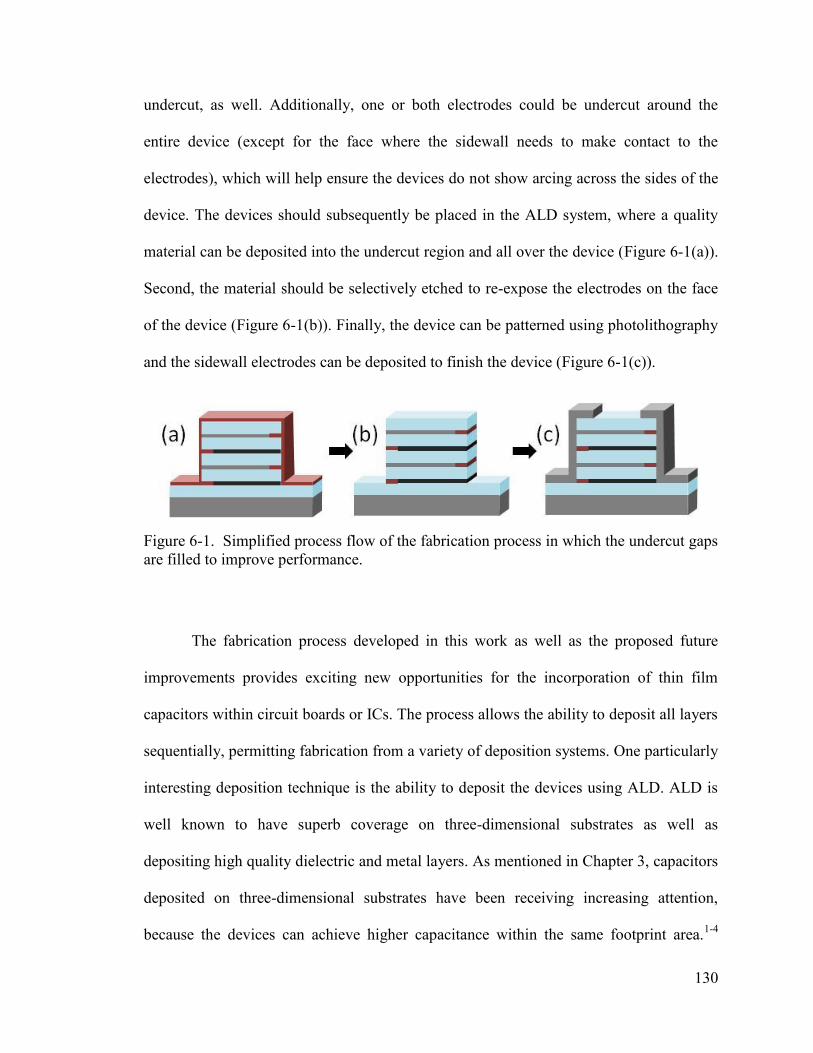
130
undercut, as well. Additionally, one or both electrodes could be undercut around the
entire device (except for the face where the sidewall needs to make contact to the
electrodes), which will help ensure the devices do not show arcing across the sides of the
device. The devices should subsequently be placed in the ALD system, where a quality
material can be deposited into the undercut region and all over the device (Figure 6-1(a)).
Second, the material should be selectively etched to re-expose the electrodes on the face
of the device (Figure 6-1(b)). Finally, the device can be patterned using photolithography
and the sidewall electrodes can be deposited to finish the device (Figure 6-1(c)).
Figure 6-1. Simplified process flow of the fabrication process in which the undercut gaps are filled to improve performance.
The fabrication process developed in this work as well as the proposed future
improvements provides exciting new opportunities for the incorporation of thin film
capacitors within circuit boards or ICs. The process allows the ability to deposit all layers
sequentially, permitting fabrication from a variety of deposition systems. One particularly
interesting deposition technique is the ability to deposit the devices using ALD. ALD is
well known to have superb coverage on three-dimensional substrates as well as
depositing high quality dielectric and metal layers. As mentioned in Chapter 3, capacitors
deposited on three-dimensional substrates have been receiving increasing attention,
because the devices can achieve higher capacitance within the same footprint area.1-4
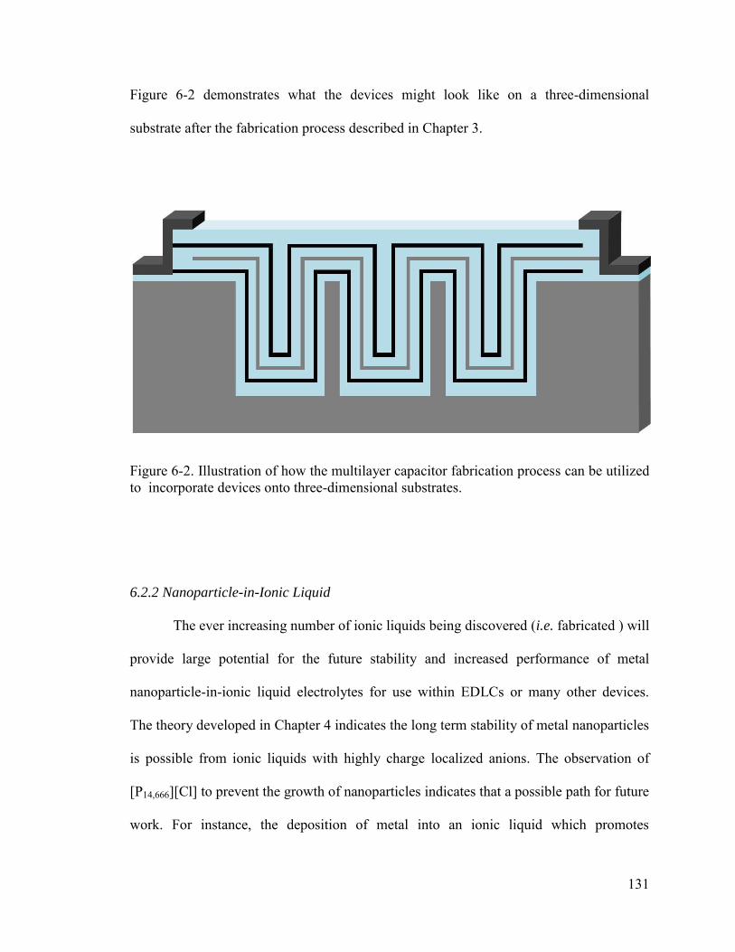
131
Figure 6-2 demonstrates what the devices might look like on a three-dimensional
substrate after the fabrication process described in Chapter 3.
Figure 6-2. Illustration of how the multilayer capacitor fabrication process can be utilized to incorporate devices onto three-dimensional substrates.
6.2.2 Nanoparticle-in-Ionic Liquid
The ever increasing number of ionic liquids being discovered (i.e. fabricated ) will
provide large potential for the future stability and increased performance of metal
nanoparticle-in-ionic liquid electrolytes for use within EDLCs or many other devices.
The theory developed in Chapter 4 indicates the long term stability of metal nanoparticles
is possible from ionic liquids with highly charge localized anions. The observation of
[P14,666][Cl] to prevent the growth of nanoparticles indicates that a possible path for future
work. For instance, the deposition of metal into an ionic liquid which promotes
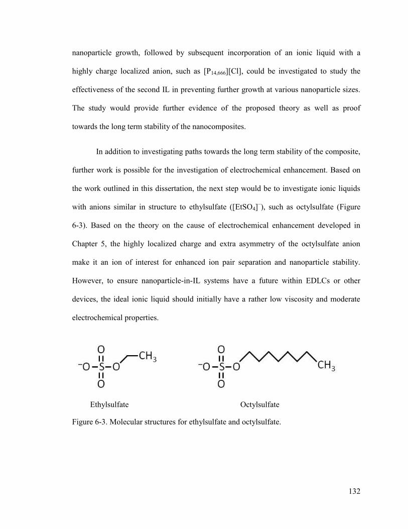
132
nanoparticle growth, followed by subsequent incorporation of an ionic liquid with a
highly charge localized anion, such as [P14,666][Cl], could be investigated to study the
effectiveness of the second IL in preventing further growth at various nanoparticle sizes.
The study would provide further evidence of the proposed theory as well as proof
towards the long term stability of the nanocomposites.
In addition to investigating paths towards the long term stability of the composite,
further work is possible for the investigation of electrochemical enhancement. Based on
the work outlined in this dissertation, the next step would be to investigate ionic liquids
with anions similar in structure to ethylsulfate ([EtSO4]–), such as octylsulfate (Figure
6-3). Based on the theory on the cause of electrochemical enhancement developed in
Chapter 5, the highly localized charge and extra asymmetry of the octylsulfate anion
make it an ion of interest for enhanced ion pair separation and nanoparticle stability.
However, to ensure nanoparticle-in-IL systems have a future within EDLCs or other
devices, the ideal ionic liquid should initially have a rather low viscosity and moderate
electrochemical properties.
Ethylsulfate Octylsulfate
Figure 6-3. Molecular structures for ethylsulfate and octylsulfate.
133
Appendix A – Further Characterization and Applications of SiOCN
The work provided in Chapter 2 was focused on the characterization methods
which would provide an understanding of how the material is grown, as well as
investigate the characteristics which would be applicable for using SiOCN as a dielectric
within thin film capacitors fabricated using microelectronic fabrication techniques, such
as those described in Chapter 3. However, much more work has been performed on
characterizing and discovering more applications of SiOCN which is worth mentioning.
Additional Characterization Methods
Mechanical Characterization
Nanoindentation experiments were conducted using an Agilent Nano Indenter
G200 using a standard XP head. The Continuous Stiffness Measurement (CSM) method
was performed on 15 regions of each sample with a constant load to loading rate ratio
held at 0.05 sec-1. The average hardness and Young’s Modulus were calculated from the
penetration depth range of 350–450 nm. The tested samples were deposited to
thicknesses >1000 nm to minimize influence of the Si substrate.
In addition, to demonstrate the feasibility of this coating as a protective layer on
polymer-based windows, a 1μm thick silane-based SiOCN deposited at 100 °C on
isopropanol cleaned polycarbonate (PC) slabs (1 in. x 3 in. x 0.2 in.) was tested under
sand-water wiper abrasion testing. For this experiment, commercial rubber windshield
wiper blades (1.5 in. long) were clamped rigidly to a solid metal backing plate with a

134
carriage weight of 1.874 lb. Arizona medium test dust (ISO 12103–1, A3; Reade
Advanced Materials) was mixed with water to a mass ratio of 53 g dust to16 kg water.
The slurry was continuously stirred in a reservoir and fed to the test surface using a
peristaltic pump with a flow rate of 1 gallon per hour. The wiper blade was cycled across
the samples up to 75,000 times. The UV–Vis transmittance and topography (using a
Veeco Optical Profilometer) with and without a SiOCN coating were measured
periodically throughout the experiment to gauge the effectiveness of the coating.
Finally, as a preliminary demonstration of the flexibility and adhesion strength of
thick silane-based SiOCN, a 10 μm thick film was deposited at 400 °C on a two inch
diameter, 800 μm thick brush-finish Al substrate cleaned with acetone sonication. The
sample was rounded around cylindrical objects with diameters ranging from 172 mm to
51 mm by pressing firmly against the objects. The sample was rounded around objects of
decreasing diameter until the SiOCN film cracked in a similar fashion as that laid out in
ASTM D522.5 Using this technique, an estimate of the strain at the time of failure was
calculated.
Direct Charge Nuclear Capacitor
Self-recharging energy storage devices using radioisotopes has gained renewed interest
due to the proposed long-term life (based on half-life of isotope), low maintenance, and
potential to reduce the batteries weight on military personnel. Our group participated in
research with a collaborator, TRACE Photonics, Inc., to investigate a direct charge
nuclear capacitor (DCNC) using SiOCN as a dielectric. DCNCs are devices which utilize
the charge of beta-emitting sources to directly charge capacitors.6, 7
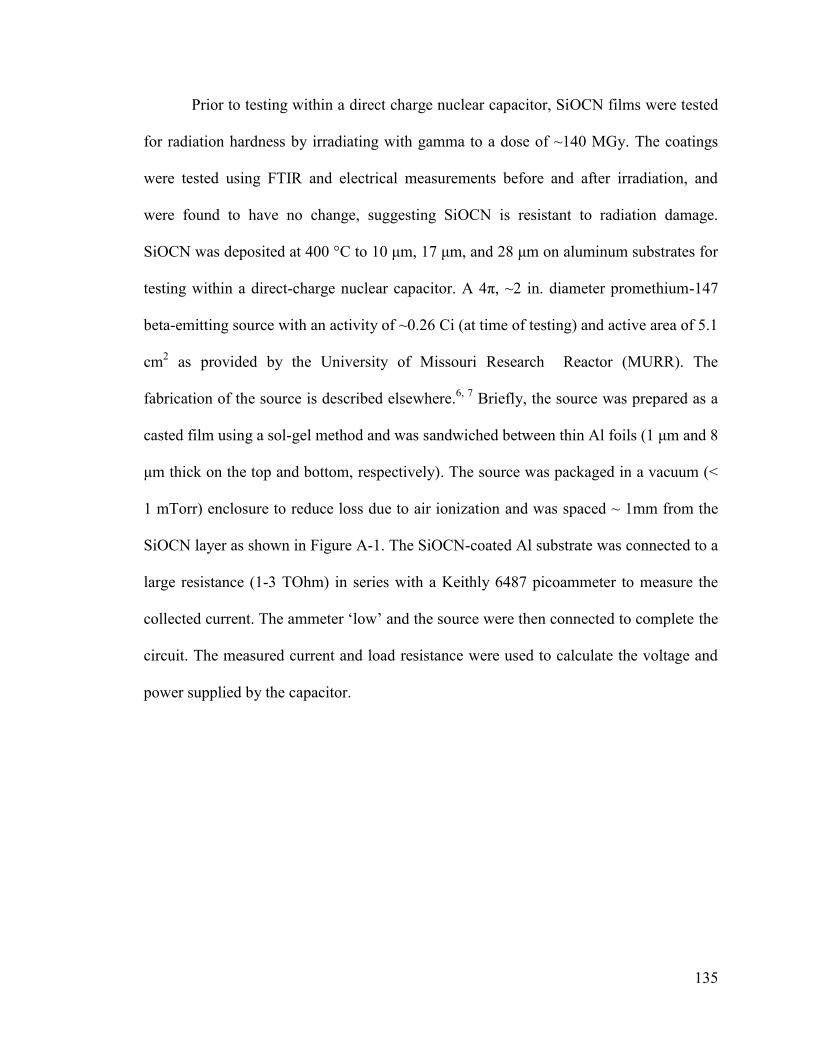
135
Prior to testing within a direct charge nuclear capacitor, SiOCN films were tested
for radiation hardness by irradiating with gamma to a dose of ~140 MGy. The coatings
were tested using FTIR and electrical measurements before and after irradiation, and
were found to have no change, suggesting SiOCN is resistant to radiation damage.
SiOCN was deposited at 400 °C to 10 μm, 17 μm, and 28 μm on aluminum substrates for
testing within a direct-charge nuclear capacitor. A 4π, ~2 in. diameter promethium-147
beta-emitting source with an activity of ~0.26 Ci (at time of testing) and active area of 5.1
cm2 as provided by the University of Missouri Research Reactor (MURR). The
fabrication of the source is described elsewhere.6, 7 Briefly, the source was prepared as a
casted film using a sol-gel method and was sandwiched between thin Al foils (1 μm and 8
μm thick on the top and bottom, respectively). The source was packaged in a vacuum (<
1 mTorr) enclosure to reduce loss due to air ionization and was spaced ~ 1mm from the
SiOCN layer as shown in Figure A-1. The SiOCN-coated Al substrate was connected to a
large resistance (1-3 TOhm) in series with a Keithly 6487 picoammeter to measure the
collected current. The ammeter ‘low’ and the source were then connected to complete the
circuit. The measured current and load resistance were used to calculate the voltage and
power supplied by the capacitor.
136
Figure A-1. Schematic of the direct charge nuclear capacitor test setup (not to scale).
Optical measurements
The refractive index (@630 nm) and thicknesses of the films deposited on Si were
measured using a J.A. Woolhams Variable Angle ellipsometer. The absorbance spectra of
the ~1 μm thick films deposited on quartz or polycarbonate were recorded from 190 nm
to 900 nm at room temperature using a Shimadzu UV–2401PC spectrophotometer.
Additional Characterization Results
Nanoindentation Hardness
Table A-1 displays the hardness and Young’s modulus obtained from the CSM
nanoindentation study. The results show that the TMS-based films have a hardness that
increases from 6.3 ± 0.2 GPa to 13.3 ± 0.2 GPa, while the silane-based films increase
from 4.8 ± 0.1 GPa to 10.4 ± 0.2 GPa as the deposition temperature increases from
100 °C to 400 °C. The higher hardness of the TMS-based films is attributed to the lower
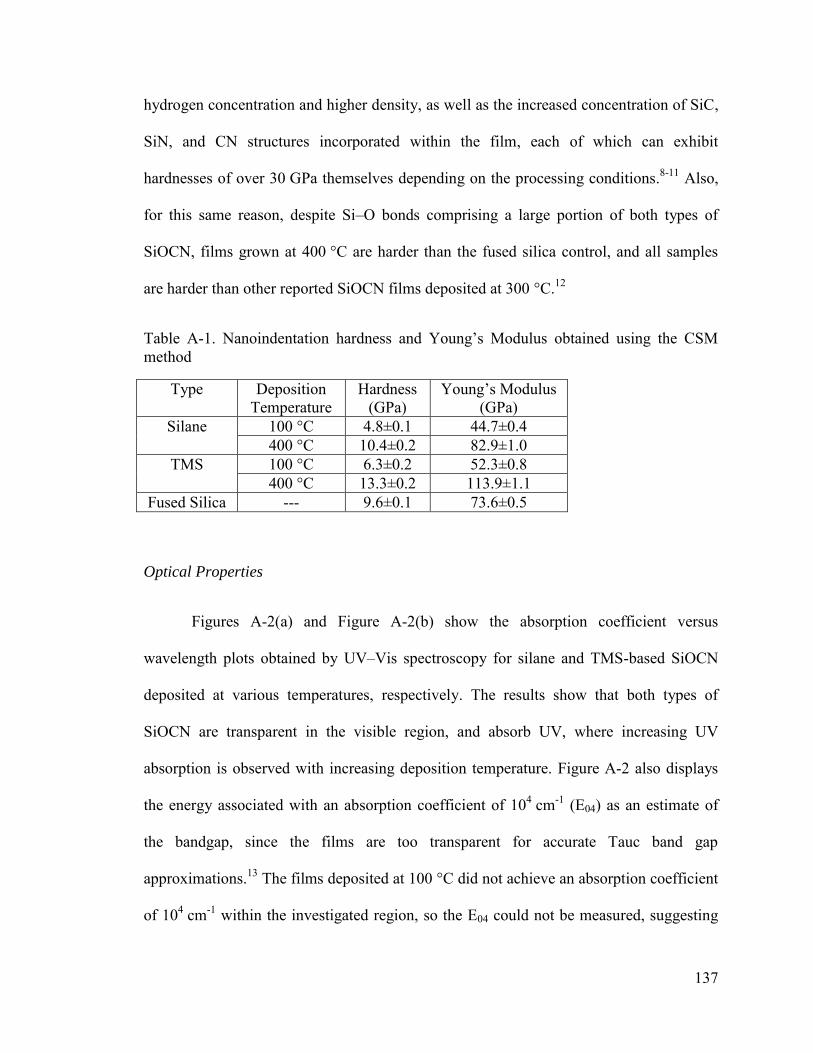
137
hydrogen concentration and higher density, as well as the increased concentration of SiC,
SiN, and CN structures incorporated within the film, each of which can exhibit
hardnesses of over 30 GPa themselves depending on the processing conditions.8-11 Also,
for this same reason, despite Si–O bonds comprising a large portion of both types of
SiOCN, films grown at 400 °C are harder than the fused silica control, and all samples
are harder than other reported SiOCN films deposited at 300 °C.12
Table A-1. Nanoindentation hardness and Young’s Modulus obtained using the CSM method
Type Deposition Temperature
Hardness (GPa)
Young’s Modulus (GPa)
Silane 100 °C 4.8±0.1 44.7±0.4 400 °C 10.4±0.2 82.9±1.0
TMS 100 °C 6.3±0.2 52.3±0.8 400 °C 13.3±0.2 113.9±1.1
Fused Silica --- 9.6±0.1 73.6±0.5
Optical Properties
Figures A-2(a) and Figure A-2(b) show the absorption coefficient versus
wavelength plots obtained by UV–Vis spectroscopy for silane and TMS-based SiOCN
deposited at various temperatures, respectively. The results show that both types of
SiOCN are transparent in the visible region, and absorb UV, where increasing UV
absorption is observed with increasing deposition temperature. Figure A-2 also displays
the energy associated with an absorption coefficient of 104 cm-1 (E04) as an estimate of
the bandgap, since the films are too transparent for accurate Tauc band gap
approximations.13 The films deposited at 100 °C did not achieve an absorption coefficient
of 104 cm-1 within the investigated region, so the E04 could not be measured, suggesting
138
the optical bandgap is larger than 6.5 eV for these samples. The large drop in the optical
band gap from 100 °C to 250 °C will be discussed later. For the 250 °C and 400 °C
depositions, the E04 for the silane films is higher than TMS films, caused by the higher
concentrations of SiO. The gap also decreases from 6.0 eV to 5.8 eV for the silane-based
film and 5.6 eV to 5.5 eV for the TMS-based film between 250 °C and 400 °C
depositions, respectively. This decrease, although small, can be attributed to the
increasing SiC concentration (reported optical band gap of around 2–3 eV)14, 15 and/or
decreasing hydrogen concentration16 within the films with increasing deposition
temperature, as demonstrated in the FTIR analysis. These measurements suggest that
either type of SiOCN is a good candidate as a transparent coating material, which will be
the subject of further discussion later.
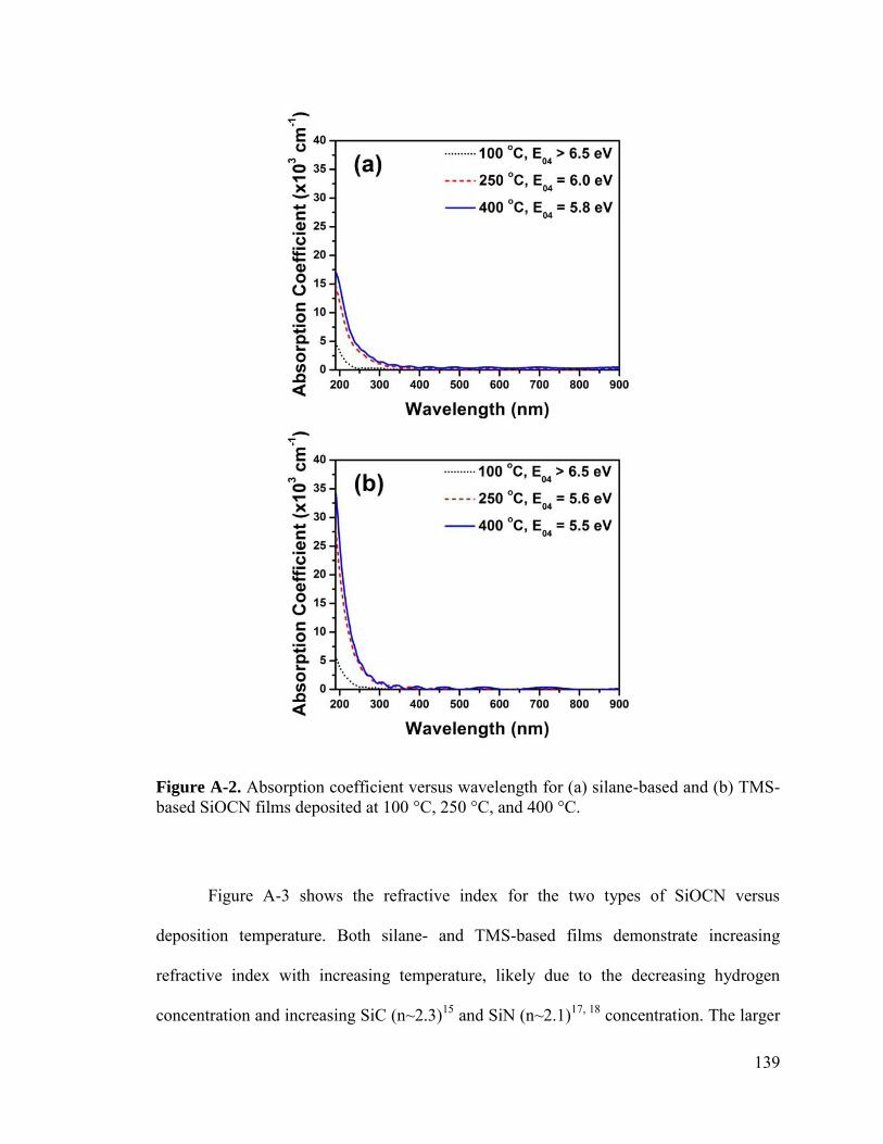
139
Figure A-2. Absorption coefficient versus wavelength for (a) silane-based and (b) TMS-based SiOCN films deposited at 100 °C, 250 °C, and 400 °C.
Figure A-3 shows the refractive index for the two types of SiOCN versus
deposition temperature. Both silane- and TMS-based films demonstrate increasing
refractive index with increasing temperature, likely due to the decreasing hydrogen
concentration and increasing SiC (n~2.3)15 and SiN (n~2.1)17, 18 concentration. The larger
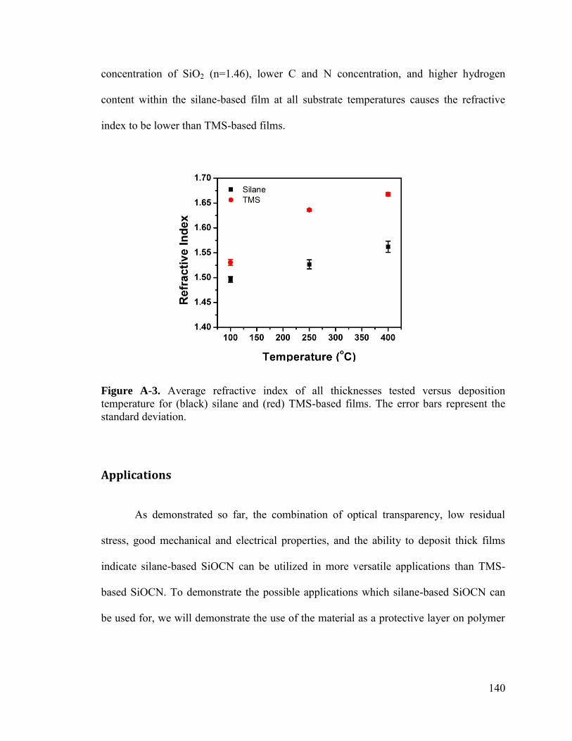
140
concentration of SiO2 (n=1.46), lower C and N concentration, and higher hydrogen
content within the silane-based film at all substrate temperatures causes the refractive
index to be lower than TMS-based films.
Figure A-3. Average refractive index of all thicknesses tested versus deposition temperature for (black) silane and (red) TMS-based films. The error bars represent the standard deviation.
Applications
As demonstrated so far, the combination of optical transparency, low residual
stress, good mechanical and electrical properties, and the ability to deposit thick films
indicate silane-based SiOCN can be utilized in more versatile applications than TMS-
based SiOCN. To demonstrate the possible applications which silane-based SiOCN can
be used for, we will demonstrate the use of the material as a protective layer on polymer
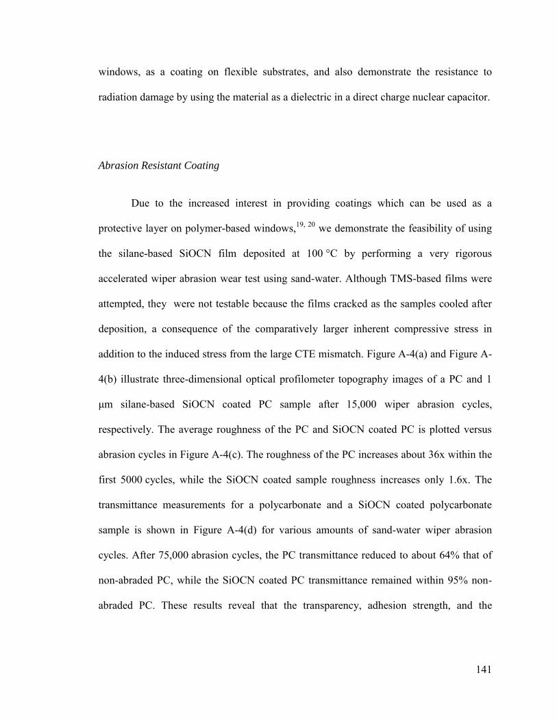
141
windows, as a coating on flexible substrates, and also demonstrate the resistance to
radiation damage by using the material as a dielectric in a direct charge nuclear capacitor.
Abrasion Resistant Coating
Due to the increased interest in providing coatings which can be used as a
protective layer on polymer-based windows,19, 20 we demonstrate the feasibility of using
the silane-based SiOCN film deposited at 100 °C by performing a very rigorous
accelerated wiper abrasion wear test using sand-water. Although TMS-based films were
attempted, they were not testable because the films cracked as the samples cooled after
deposition, a consequence of the comparatively larger inherent compressive stress in
addition to the induced stress from the large CTE mismatch. Figure A-4(a) and Figure A-
4(b) illustrate three-dimensional optical profilometer topography images of a PC and 1
μm silane-based SiOCN coated PC sample after 15,000 wiper abrasion cycles,
respectively. The average roughness of the PC and SiOCN coated PC is plotted versus
abrasion cycles in Figure A-4(c). The roughness of the PC increases about 36x within the
first 5000 cycles, while the SiOCN coated sample roughness increases only 1.6x. The
transmittance measurements for a polycarbonate and a SiOCN coated polycarbonate
sample is shown in Figure A-4(d) for various amounts of sand-water wiper abrasion
cycles. After 75,000 abrasion cycles, the PC transmittance reduced to about 64% that of
non-abraded PC, while the SiOCN coated PC transmittance remained within 95% non-
abraded PC. These results reveal that the transparency, adhesion strength, and the
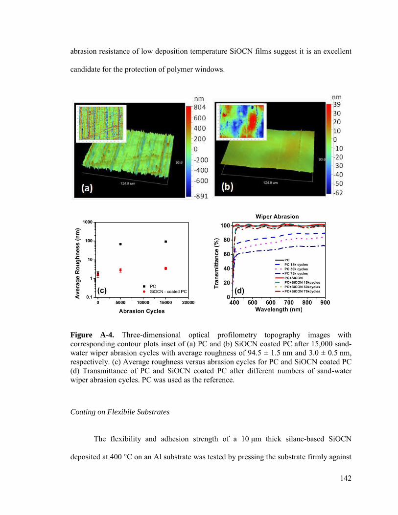
142
abrasion resistance of low deposition temperature SiOCN films suggest it is an excellent
candidate for the protection of polymer windows.
Figure A-4. Three-dimensional optical profilometry topography images with corresponding contour plots inset of (a) PC and (b) SiOCN coated PC after 15,000 sand-water wiper abrasion cycles with average roughness of 94.5 ± 1.5 nm and 3.0 ± 0.5 nm, respectively. (c) Average roughness versus abrasion cycles for PC and SiOCN coated PC (d) Transmittance of PC and SiOCN coated PC after different numbers of sand-water wiper abrasion cycles. PC was used as the reference.
Coating on Flexibile Substrates
The flexibility and adhesion strength of a 10 μm thick silane-based SiOCN
deposited at 400 °C on an Al substrate was tested by pressing the substrate firmly against
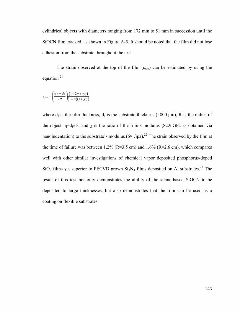
143
cylindrical objects with diameters ranging from 172 mm to 51 mm in succession until the
SiOCN film cracked, as shown in Figure A-5. It should be noted that the film did not lose
adhesion from the substrate throughout the test.
The strain observed at the top of the film (εtop) can be estimated by using the
equation 21
1 22 1 1
ftop
d ds
R
where df is the film thickness, ds is the substrate thickness (~800 μm), R is the radius of
the object, η=df/ds, and χ is the ratio of the film’s modulus (82.9 GPa as obtained via
nanoindentation) to the substrate’s modulus (69 Gpa).22 The strain observed by the film at
the time of failure was between 1.2% (R=3.5 cm) and 1.6% (R=2.6 cm), which compares
well with other similar investigations of chemical vapor deposited phosphorus-doped
SiO2 films yet superior to PECVD grown Si3N4 films deposited on Al substrates.23 The
result of this test not only demonstrates the ability of the silane-based SiOCN to be
deposited to large thicknesses, but also demonstrates that the film can be used as a
coating on flexible substrates.
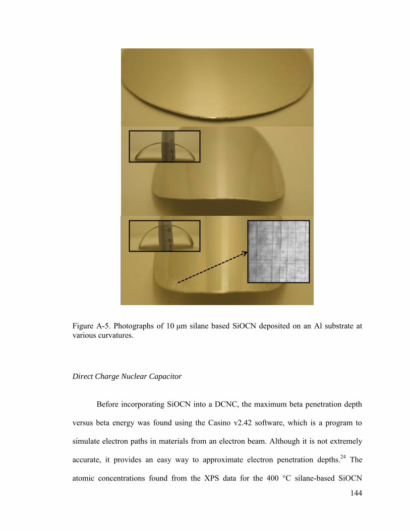
144
Figure A-5. Photographs of 10 μm silane based SiOCN deposited on an Al substrate at various curvatures.
Direct Charge Nuclear Capacitor
Before incorporating SiOCN into a DCNC, the maximum beta penetration depth
versus beta energy was found using the Casino v2.42 software, which is a program to
simulate electron paths in materials from an electron beam. Although it is not extremely
accurate, it provides an easy way to approximate electron penetration depths.24 The
atomic concentrations found from the XPS data for the 400 °C silane-based SiOCN
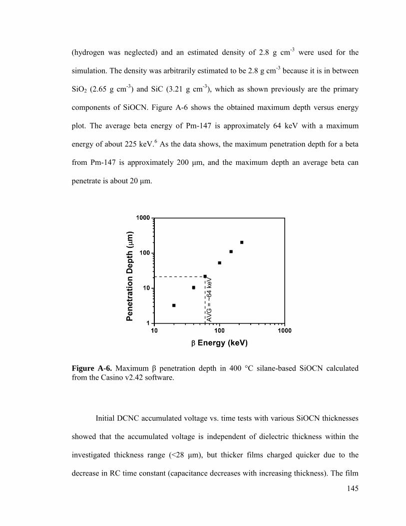
145
(hydrogen was neglected) and an estimated density of 2.8 g cm-3 were used for the
simulation. The density was arbitrarily estimated to be 2.8 g cm-3 because it is in between
SiO2 (2.65 g cm-3) and SiC (3.21 g cm-3), which as shown previously are the primary
components of SiOCN. Figure A-6 shows the obtained maximum depth versus energy
plot. The average beta energy of Pm-147 is approximately 64 keV with a maximum
energy of about 225 keV.6 As the data shows, the maximum penetration depth for a beta
from Pm-147 is approximately 200 μm, and the maximum depth an average beta can
penetrate is about 20 μm.
Figure A-6. Maximum β penetration depth in 400 °C silane-based SiOCN calculated from the Casino v2.42 software.
Initial DCNC accumulated voltage vs. time tests with various SiOCN thicknesses
showed that the accumulated voltage is independent of dielectric thickness within the
investigated thickness range (<28 μm), but thicker films charged quicker due to the
decrease in RC time constant (capacitance decreases with increasing thickness). The film
146
thickness does not affect the accumulated voltage because high concentrations of the
emitted beta are able to penetrate completely through the SiOCN layer within the
investigated thickness range.
A 10 μm thick SiOCN dielectric was then measured with a 1 TΩ and 3 TΩ load
resistor to measure the effects of load resistance. Figure A-7(a) shows the accumulated
voltage versus time. The collected current from the device was approximately 145 pA
(Figure A-7(b)), resulting in accumulated voltages of about 150 V and 450 V for the
1 TΩ and 3 TΩ load, respectively. Since the measurement only accounts for the beta
collected from one side of the source, we can assume the maximum available charging
current from beta is approximately 770 pA. The measured current was about 145 pA for
both load resistances, meaning the capacitor is collecting roughly 19% of the maximum
available current from the beta alone. Some of the loss may be due to any remaining air
in the test setup or the sample holders, which will ionize and promote conduction away
from the dielectric, electron trajectories not falling onto the dielectric (due to the spacer),
and the backscattering of electrons which will increase with increasing potential. With a
3 TΩ load, the output power of the device reached about 60 nW.
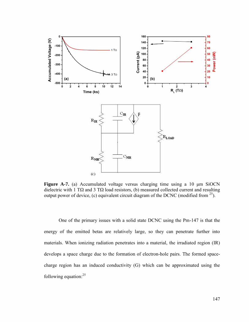
147
Figure A-7. (a) Accumulated voltage versus charging time using a 10 μm SiOCN dielectric with 1 TΩ and 3 TΩ load resistors, (b) measured collected current and resulting output power of device, (c) equivalent circuit diagram of the DCNC (modified from 25).
One of the primary issues with a solid state DCNC using the Pm-147 is that the
energy of the emitted betas are relatively large, so they can penetrate further into
materials. When ionizing radiation penetrates into a material, the irradiated region (IR)
develops a space charge due to the formation of electron-hole pairs. The formed space-
charge region has an induced conductivity (G) which can be approximated using the
following equation:25
148
0.5 1oo
DG G
D
(A-1)
where D is the absorbed dose rate, Do is a reference dose rate, Go is the conductivity at
Do, and Δ is the trap and energy distribution constant. For a rough approximation, if we
take a source with an activity of 0.26 Ci and a stopping power of 4.857 MeV cm2 g-1 for a
beta energy of 60 keV (calculated from the NIST ESTAR program),26 a film thickness of
10 μm would acquire a dose rate of ~0.18 Gy s-1. Accordingly, the resistivity of the film
will decrease at least a few orders.27 A 10 μm SiOCN film on a 2 in. diameter substrate
and a resistivity on the order of 1017 Ω cm (from Chapter 2) results in a film resistance of
about 5 TΩ. Referring to the provided DCNC circuit model in Figure A-7(c), the
resistance of the non-irradiated region (NIR) for these SiOCN films is non-existent since
the beta can penetrate completely through the dielectric (RNIR is shorted). Without any
induced conductivity, if the source were to be placed directly on the dielectric to conserve
space, the maximum possible current (assuming all emitted beta charge is collected)
through a 1 TΩ load is reduced to 83.3% (50% for a 5 TΩ load, etc. since RIR || RLOAD).
Therefore, it is clearly indicated that any induced conductivity would be completely
detrimental to device performance if the vacuum spacer were to be removed. This issue
can be resolved by switching to a source with much lower beta energy (and thus lower
penetration depth), or by increasing the thickness of the dielectric until it is much thicker
than the maximum penetration depth. The TRACE Photonics group had much more
success using the former, with a tritium source and a polyimide dielectric.28 Regardless,
this experiment verified SiOCN’s radiation hardness and potential as a dielectric within
radioisotope devices.
149
Multi-layer dielectrics
The excellent electrical properties of the SiOCN films indicate that it can be used
as a dielectric material itself or as a coating to improve the electrical properties of a base
material. As a proof-of-concept, the organosilicate polymer poly(methylsilsesquioxane)
(PMSSQ) film was spin coated to about 1.5 μm thick followed by 0.5 μm silane based
SiOCN deposition. The dielectric properties of polymer materials are degraded by their
inherent voids, which leads to decreased breakdown strength and inconsistency (Figure
A-8(a)). For this film, the breakdown strength was 0.5 ± 0.4 MV cm-1. As shown in
Figure A-8(b), the reliability and breakdown strength of the final two-layer film was
significantly improved post SiOCN deposition, with all devices studying showing
breakdown >1 MV cm-1. Despite the capacitance of the device decreasing from ~4.6 pF
to 3.6 pF after deposition, the increase in voltage from a maximum of 150 V to at least
300 V is sufficient enough to increase the overall energy density at least 2x.
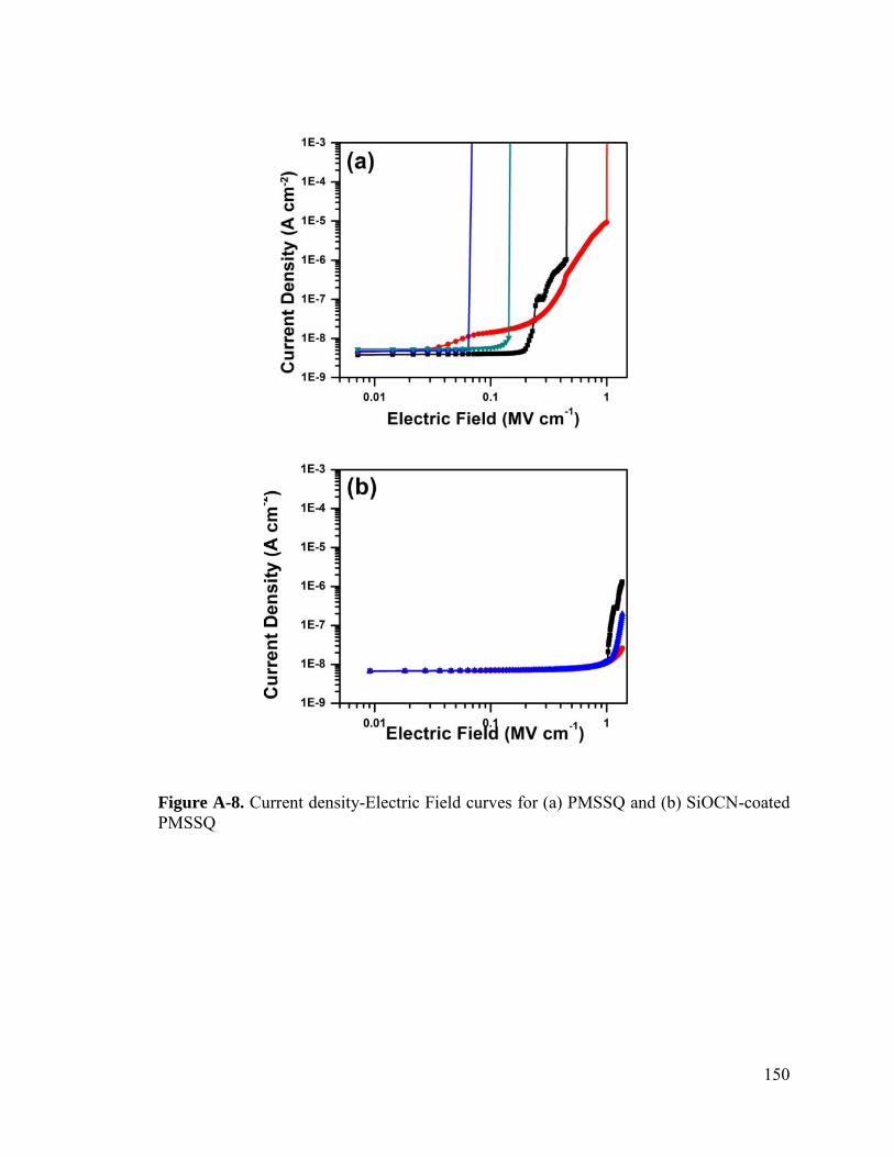
150
Figure A-8. Current density-Electric Field curves for (a) PMSSQ and (b) SiOCN-coated PMSSQ
151
References
1. Detalle, M.; Barrenetxea, M.; Muller, P.; Potoms, G.; Phommahaxay, A.; Soussan, P.; Vaesen, K.; De Raedt, W., High density, low leakage Back-End 3D capacitors for mixed signals applications. Microelectron. Eng. 2010, 87, 2571-2576.
2. Banerjee, P.; Perez, I.; Henn-Lecordier, L.; Lee, S. B.; Rubloff, G. W., Nanotubular metal–insulator–metal capacitor arrays for energy storage. Nature
Nanotechnology 2009, 4, 292-296.
3. Banerjee, P.; Perez, I.; Henn-Lecordier, L.; Lee, S. B.; Rubloff, G. W., ALD based Metal-insulator-metal (MIM) Nanocapacitors for Energy Storage. ECS
Transactions 2009, 25, 345-353.
4. Nongaillard, M.; Lallemand, F.; Allard, B., Design for manufacturing of 3D capacitors. Microelectron. J. 2010, 41, 845-850.
5. ASTM Standard D522M - 13, "Standard Test Methods for Mandrel Bend Test of Attached Organic Coatings". ASTM International: West Conshohocken, PA, 1939 (2013).
6. Kavetskiy, A.; Yakubova, G.; Lin, Q.; Chan, D.; Yousaf, S. M.; Bower, K.; Robertson, J. D.; Garnov, A.; Meier, D., Promethium-147 capacitor. Appl. Radiat. Isot.
2009, 67, 1057-1062.
7. Kavetskiy, A.; Yakubova, G.; Yousaf, S. M.; Bower, K.; Robertson, J. D.; Garnov, A., Efficiency of Pm-147 direct charge radioisotope battery. Appl. Radiat. Isot.
2011, 69, 744-748.
8. Yoshino, M.; Shimozuma, M.; Date, H.; Itoh, H.; Tagashira, H., Deposition of SiC films by ion-enhanced plasma chemical vapor deposition using tetramethylsilane+H2. Thin Solid Films 2005, 492, 207-211.
9. Jung, Y.-G.; Lawn, B. R.; Martyniuk, M.; Huang, H.; Hu, X. Z., Evaluation of elastic modulus and hardness of thin films by nanoindentation. J. Mater. Res. 2004, 19, 3076-3080.
152
10. El Khakani, M.; Chaker, M.; Jean, A.; Boily, S.; Kieffer, J.; O'hern, M.; Ravet, M.; Rousseaux, F., Hardness and Young's modulus of amorphous a-SiC thin films determined by nanoindentation and bulge tests. J. Mater. Res. 1994, 9, 96-103.
11. Ogata, K.; Chubaci, J. F. D.; Fujimoto, F., Properties of carbon nitride films with composition ratio C/N= 0.5–3.0 prepared by the ion and vapor deposition method. J.
Appl. Phys. 1994, 76, 3791-3796.
12. Zhou, Y.; Probst, D.; Thissen, A.; Kroke, E.; Riedel, R.; Hauser, R.; Hoche, H.; Broszeit, E.; Kroll, P.; Stafast, H., Hard silicon carbonitride films obtained by RF-plasma-enhanced chemical vapour deposition using the single-source precursor bis(trimethylsilyl)carbodiimide. J. Eur. Ceram. Soc. 2006, 26, 1325-1335.
13. Tauc, J.; Grigorovici, R.; Vancu, A., Optical properties and electronic structure of amorphous germanium. physica status solidi (b) 1966, 15, 627-637.
14. Rajagopalan, T.; Wang, X.; Lahlouh, B.; Ramkumar, C.; Dutta, P.; Gangopadhyay, S., Low temperature deposition of nanocrystalline silicon carbide films by plasma enhanced chemical vapor deposition and their structural and optical characterization. J. Appl. Phys. 2003, 94, 5252-5260.
15. Racine, B.; Ferrari, A.; Morrison, N.; Hutchings, I.; Milne, W.; Robertson, J., Properties of amorphous carbon–silicon alloys deposited by a high plasma density source. J. Appl. Phys. 2001, 90, 5002-5012.
16. Hama, T.; Okamoto, H.; Hamakawa, Y.; Matsubara, T., Hydrogen content dependence of the optical energy gap in a-Si:H. J. Non-Cryst. Solids 1983, 59–60, Part 1, 333-336.
17. Gunde, M. K.; Maček, M., The relationship between the macroscopic properties of PECVD silicon nitride and oxynitride layers and the characteristics of their networks. Appl. Phys. A 2002, 74, 181-186.
18. Rocheleau, R. E.; Zhang, Z.; Niles, D. W.; Mason, A., Effect of hydrogen dilution on the properties and bonding in plasma‐deposited silicon nitride. J. Appl. Phys. 1992, 72, 282-284.
19. Noborisaka, M.; Kodama, H.; Nagashima, S.; Shirakura, A.; Horiuchi, T.; Suzuki, T., Synthesis of transparent and hard SiOC (− H) thin films on polycarbonate substrates by PECVD method. Surf. Coat. Technol. 2012, 206, 2581-2584.
153
20. Fabbri, P.; Messori, M.; Toselli, M.; Veronesi, P.; Rocha, J.; Pilati, F., Enhancing the scratch resistance of polycarbonate with poly (Ethylene oxide)–silica hybrid coatings. Adv. Polym. Tech. 2008, 27, 117-126.
21. Suo, Z.; Ma, E.; Gleskova, H.; Wagner, S., Mechanics of rollable and foldable film-on-foil electronics. Appl. Phys. Lett. 1999, 74, 1177-1179.
22. Ledbetter, H., Physical Properties Data Compilations Relevant to Energy
Storage. National Bureau of Standards: 1982.
23. Scafidi, P.; Ignat, M., Cracking and loss of adhesion of Si3N4 and SiO2: P films deposited on Al substrates. J. Adhes. Sci. Technol. 1998, 12, 1219-1242.
24. Drouin, D.; Couture, A. R.; Joly, D.; Tastet, X.; Aimez, V.; Gauvin, R., CASINO V2.42—A Fast and Easy-to-use Modeling Tool for Scanning Electron Microscopy and Microanalysis Users. Scanning 2007, 29, 92-101.
25. Gross, B., Radiation-induced charge storage and polarization effects. In Electrets, Springer: 1987; pp 217-284.
26. Berger, M. J., J. S. Coursey, M. A. Zucker, J. Chang Stopping-Power and Range Tables for Electrons, Protons, and Helium Ions. http://physics.nist.gov/PhysRefData/Star/Text/ESTAR.html (accessed August).
27. Tanaka, T.; Suzuki, A.; Muroga, T.; Sato, F.; Iida, T.; Nishitani, T., Radiation induced conductivity of ceramic coating materials under 14 MeV neutron irradiation. J.
Nucl. Mater. 2004, 329–333, Part B, 1434-1437.
28. Yakubova, G. N. Nuclear batteries with tritium and promethium-147 radioactive sources. University of Illinois, 2010.
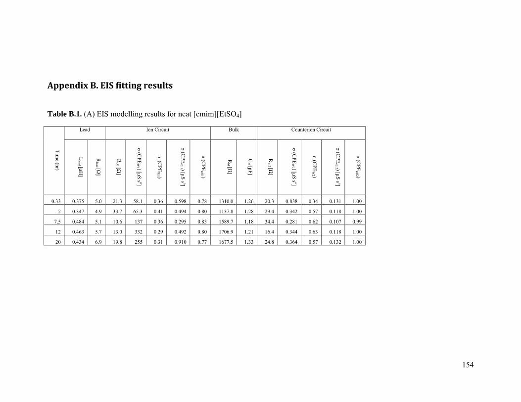
154
Appendix B. EIS fitting results
Table B.1. (A) EIS modelling results for neat [emim][EtSO4]
Time (hr)
Lead Ion Circuit Bulk Counterion Circuit
Llead [μH
]
Rlead [Ω
]
Rct1 [Ω
]
σ (CPE
W1 ) [μS s n]
n (CPE
W1 )
σ (CPE
cdl1 ) [μS s n]
n (CPE
cdl1 )
Rhf [Ω
]
Chf [pF]
R ct2 [Ω
]
σ (CPE
W2 ) [μS s n]
n (CPE
W2 )
σ (CPE
cdl2 ) [μS s n]
n (CPE
cdl2 )
0.33 0.375 5.0 21.3 58.1 0.36 0.598 0.78 1310.0 1.26 20.3 0.838 0.34 0.131 1.00
2 0.347 4.9 33.7 65.3 0.41 0.494 0.80 1137.8 1.28 29.4 0.342 0.57 0.118 1.00
7.5 0.484 5.1 10.6 137 0.36 0.295 0.83 1589.7 1.18 34.4 0.281 0.62 0.107 0.99
12 0.463 5.7 13.0 332 0.29 0.492 0.80 1706.9 1.21 16.4 0.344 0.63 0.118 1.00
20 0.434 6.9 19.8 255 0.31 0.910 0.77 1677.5 1.33 24.8 0.364 0.57 0.132 1.00
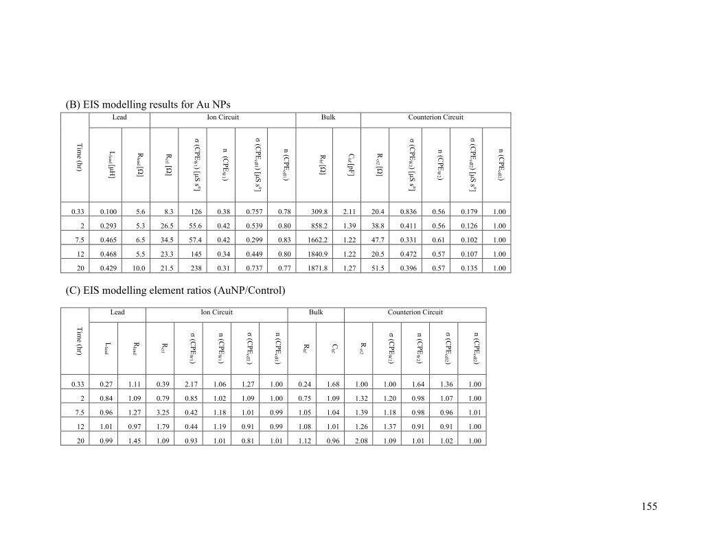
155
(B) EIS modelling results for Au NPs
Time (hr)
Lead Ion Circuit Bulk Counterion Circuit
Llead [μH
]
Rlead [Ω
]
Rct1 [Ω
]
σ (CPE
W1 ) [μS s n]
n (CPE
W1 )
σ (CPE
cdl1 ) [μS s n]
n (CPE
cdl1 )
Rhf [Ω
]
Chf [pF]
R ct2 [Ω
]
σ (CPE
W2 ) [μS s n]
n (CPE
W2 )
σ (CPE
cdl2 ) [μS s n]
n (CPE
cdl2 ) 0.33 0.100 5.6 8.3 126 0.38 0.757 0.78 309.8 2.11 20.4 0.836 0.56 0.179 1.00
2 0.293 5.3 26.5 55.6 0.42 0.539 0.80 858.2 1.39 38.8 0.411 0.56 0.126 1.00
7.5 0.465 6.5 34.5 57.4 0.42 0.299 0.83 1662.2 1.22 47.7 0.331 0.61 0.102 1.00
12 0.468 5.5 23.3 145 0.34 0.449 0.80 1840.9 1.22 20.5 0.472 0.57 0.107 1.00
20 0.429 10.0 21.5 238 0.31 0.737 0.77 1871.8 1.27 51.5 0.396 0.57 0.135 1.00 (C) EIS modelling element ratios (AuNP/Control)
Time (hr)
Lead Ion Circuit Bulk Counterion Circuit
Llead
Rlead
Rct1
σ (CPE
W1 )
n (CPE
W1 )
σ (CPE
cdl1 )
n (CPE
cdl1 )
Rhf
Chf
R ct2
σ (CPE
W2 )
n (CPE
W2 )
σ (CPE
cdl2 )
n (CPE
cdl2 )
0.33 0.27 1.11 0.39 2.17 1.06 1.27 1.00 0.24 1.68 1.00 1.00 1.64 1.36 1.00
2 0.84 1.09 0.79 0.85 1.02 1.09 1.00 0.75 1.09 1.32 1.20 0.98 1.07 1.00
7.5 0.96 1.27 3.25 0.42 1.18 1.01 0.99 1.05 1.04 1.39 1.18 0.98 0.96 1.01
12 1.01 0.97 1.79 0.44 1.19 0.91 0.99 1.08 1.01 1.26 1.37 0.91 0.91 1.00
20 0.99 1.45 1.09 0.93 1.01 0.81 1.01 1.12 0.96 2.08 1.09 1.01 1.02 1.00
156
Vita
Steven C. Hamm was born in Kansas City, Missouri on March 29, 1987. He
received his Bachelor of Science in Electrical Engineering from the University of
Missouri in 2009. Following a year of undergraduate research, he enrolled as a graduate
student under the advisement of Dr. Shubhra Gangopadhyay. He will be receiving his
PhD in Electrical and Computer Engineering in June 2014. He is a very hands-on person
and enjoys working with new equipment and learning new techniques. His current
research interests are very diverse, but he enjoys researching the advancement of energy
storage and harvesting devices.


